Growth Dynamics of SemiconductorNanostructures by MOCVD
Kai Fu
Department of Theoretical Chemistry
School of Biotechnology
Royal Institute of Technology
Stockholm, Sweden 2009

c© Kai Fu, 2009
ISBN 978-91-7415-470-2
TRITA-BIO Report 2009:22
ISSN 1654-2312
Printed by Universitetsservice US AB, Stockholm, Sweden, 2009
3
Abstract
Semiconductors and related low-dimensional nanostructures are extremely impor-
tant in the modern world. They have been extensively studied and applied in
industry/military areas such as ultraviolet optoelectronics, light emitting diodes,
quantum-dot photodetectors and lasers. The knowledge of growth dynamics of semi-
conductor nanostructures by metalorganic chemical vapour deposition (MOCVD) is
very important then. MOCVD, which is widely applied in industry, is a kind of
chemical vapour deposition method of epitaxial growth for compound semiconduc-
tors. In this method, one or several of the precursors are metalorganics which contain
the required elements for the deposit materials. Theoretical studies of growth mech-
anism by MOCVD from a realistic reactor dimension down to atomic dimensions
can give fundamental guidelines to the experiment, optimize the growth conditions
and improve the quality of the semiconductor-nanostructure-based devices.
Two main types of study methods are applied in the present thesis in order to
understand the growth dynamics of semiconductor nanostructures at the atomic
level: (1) Kinetic Monte Carlo method which was adopted to simulate film growths
such as diamond, Si, GaAs and InP using the chemical vapor deposition method;
(2) Computational fluid dynamics method to study the distribution of species and
temperature in the reactor dimension. The strain energy is introduced by short-
range valence-force-field method in order to study the growth process of the hetero
epitaxy.
The Monte Carlo studies show that the GaN film grows on GaN substrate in a
two-dimensional step mode because there is no strain over the surface during ho-
moepitaxial growth. However, the growth of self-assembled GaSb quantum dots
(QDs) on GaAs substrate follows strain-induced Stranski-Krastanov mode. The
formation of GaSb nanostructures such as nanostrips and nanorings could be de-
termined by the geometries of the initial seeds on the surface. Furthermore, the
growth rate and aspect ratio of the GaSb QD are largely determined by the strain
field distribution on the growth surface.
4
Preface
The work presented in this thesis has been carried out at the Department of The-
oretical Chemistry, School of Biotechnology, Royal Institute of Technology (KTH),
Stockholm, Sweden.
Paper I Kai Fu, Y. Fu, P. Han, Y. Zhang and R. Zhang, Kinetic Monte Carlo
study of metal organic chemical vapour deposition growth dynamics of GaN thin
film at microscopic level, J. Appl. Phys. 103, 103524, 2008.
Paper II Kai Fu and Y. Fu, Kinetic Monte Carlo study of metal organic chemical
vapour deposition growth mechanism of GaSb quantum dots, Appl. Phys. Lett. 93,
101906, 2008.
Paper III Kai Fu and Y. Fu, Growth dynamics of GaSb quantum dots in strain-
induced Stranski-Krastanov mode. 2008 Sino-Swedish Workshop on Novel Semicon-
ductor Optoelectronic Materials and Devices, June 16-17, 2008, Gothenburg.
Paper IV Kai Fu and Y. Fu, Strain-induced Stranski-Krastanov three dimen-
sional growth mode of GaSb quantum dot on GaAs substrate, Appl. Phys. Lett.
94, 181913, 2009.
Paper V X.-F. Yang, Kai Fu, W. Lu, W.-L. Xu, and Y. Fu, Strain effect in
determining the geometric shape of self-assembled quantum dot, J. Phys. D: Appl.
Phys. 42, 125414, 2009.
Paper VI Kai Fu and Y. Fu, Kinetic Monte Carlo study of stacked GaSb quan-
tum dot MOCVD growth. Manuscript.

5
Comments on my contribution to the papers included
• I was responsible for all calculations and writing of papers I, II, III, IV, and
VI.
• I was responsible for discussion about the VFF-related calculations in paper
V.
6
Acknowledgments
First of all, I would like to express my intense gratitude to my supervisor Dr. Ying
Fu, who led me into the interesting research field of growth dynamics of nanostruc-
tures and helped me fulfill my PhD study. I am really impressed by his deep insight
to the nature of physics.
I am also grateful to Prof. Hans Agen for giving me the opportunity to work in this
wonderful department.
I deeply appreciate Prof. Yi Luo and his family for their warm-hearted help. Thanks
to Prof. Ping Han, my previous supervisor in Nanjing University for introducing me
to study in Sweden.
Many Thanks to Dr. X.-F. Yang in Shanghai Institute of Technical Physics for kind
help and fruitful cooperation. Special thanks to Dr. TT and Liu Kai who helped
me at the beginning of my study and life in Sweden. I would like to express my
sincere appreciation to all of the colleagues in our department at KTH. It is really
a great time to be with you guys in Sweden.
Finally, special thanks for my parents for their constant love and support.
Computing resources was acknowledged from the Swedish National Infrastructure
for Computing.
Kai Fu
Contents
1 Introduction 9
1.1 Brief introduction to semiconductor industry . . . . . . . . . . . . . . 9
1.2 Why theoretical studies . . . . . . . . . . . . . . . . . . . . . . . . . . 11
1.3 Overview of my study subjects and results . . . . . . . . . . . . . . . 13
1.3.1 GaN film growth . . . . . . . . . . . . . . . . . . . . . . . . . 13
1.3.2 GaSb QD growth . . . . . . . . . . . . . . . . . . . . . . . . . 14
1.3.3 Surface growth and strain field . . . . . . . . . . . . . . . . . 15
1.4 Thesis construction . . . . . . . . . . . . . . . . . . . . . . . . . . . . 15
2 Electronic and optical properties 17
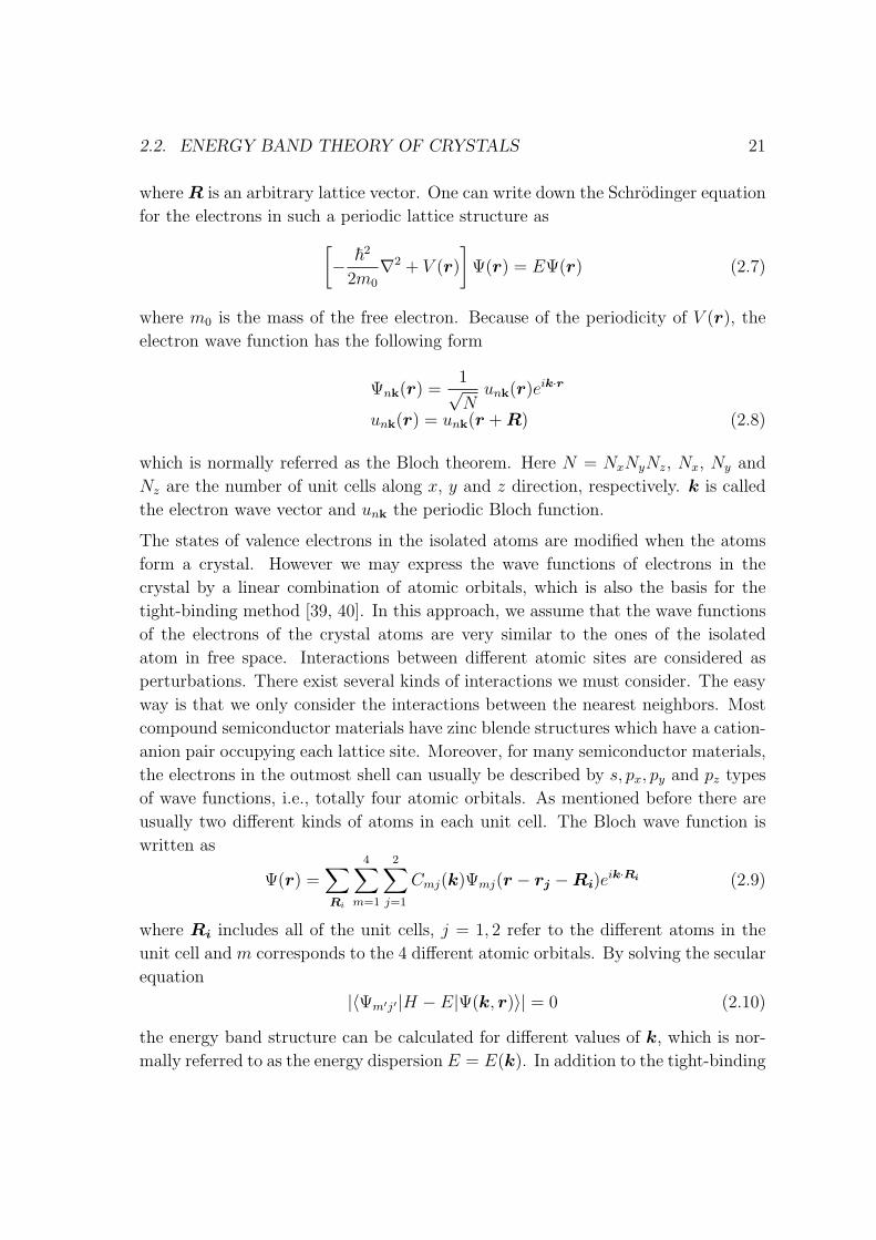
2.1 Geometrical lattice structure of semiconductors . . . . . . . . . . . . 17
2.2 Energy band theory of crystals . . . . . . . . . . . . . . . . . . . . . . 20
2.3 Band structures of III-V semiconductors . . . . . . . . . . . . . . . . 22
2.4 Applications of III-V semiconductors . . . . . . . . . . . . . . . . . . 25
2.5 Knowledge about III-V compound growth . . . . . . . . . . . . . . . 28
3 Thin film and QD growth by MOCVD 31
3.1 Basic principle of MOCVD growth . . . . . . . . . . . . . . . . . . . 31
3.2 GaN and GaSb MOCVD growths . . . . . . . . . . . . . . . . . . . . 32
3.3 Nucleation and growth on hetero substrate . . . . . . . . . . . . . . . 34
4 Chemical kinetics 37
7

8 CONTENTS
4.1 Rate of reaction . . . . . . . . . . . . . . . . . . . . . . . . . . . . . . 37
4.2 Rate laws and rate constants . . . . . . . . . . . . . . . . . . . . . . . 39
4.3 Factors affecting reaction rate . . . . . . . . . . . . . . . . . . . . . . 39
4.4 Theories about reaction rates . . . . . . . . . . . . . . . . . . . . . . 40
4.5 Rate law with simple order . . . . . . . . . . . . . . . . . . . . . . . . 43
5 Computational fluid dynamics method 45
5.1 Fundamental assumptions . . . . . . . . . . . . . . . . . . . . . . . . 46
5.2 Navier-Stokes equations . . . . . . . . . . . . . . . . . . . . . . . . . 47
5.3 Brief introduction of CFD-ACE+ . . . . . . . . . . . . . . . . . . . . 49
5.4 Application: Thin film growth . . . . . . . . . . . . . . . . . . . . . . 50
6 Kinetic Monte Carlo method 53
6.1 Principles of KMC method . . . . . . . . . . . . . . . . . . . . . . . . 53
6.2 GaN film growth simulated by KMC method . . . . . . . . . . . . . . 63
6.3 Valence-force-field approach . . . . . . . . . . . . . . . . . . . . . . . 66
6.4 GaSb QD growth simulated by KMC method . . . . . . . . . . . . . 68
6.5 Explanation about my code . . . . . . . . . . . . . . . . . . . . . . . 73
7 Comments on included papers 77
Chapter 1
Introduction
The complexity for minimum component costs has increased at a rate of
roughly a factor of two per year ... Certainly over the short term this
rate can be expected to continue, if not to increase. Over the longer term,
the rate of increase is a bit more uncertain, although there is no reason
to believe it will not remain nearly constant for at least 10 years. That
means by 1975, the number of components per integrated circuit for min-
imum cost will be 65,000. I believe that such a large circuit can be built
on a single wafer.
Moore’s Law, Gordon E. Moore Electronics Magazine April 19, 1965
1.1 Brief introduction to semiconductor industry
The semiconductor industry is involved in design and fabrication of semiconductor
devices. It was formed in the 1960s and has become the most important part in the
industry field. The market share reached as high as 249 billion dollars in 2008 [1].
Due to such a development of the semiconductor industry, information technology
(IT) can be observed in all detailed aspects of people’s daily life. Computers, mobile
phones, internet... are most well known. The semiconductor industry does not only
bring us with IT that improves our daily life and helps us communicate with each
other in an easy way, it also changes many other traditional industries and also
agriculture. The improvement in measurement, analysis, calculation, and control
technology improves efficiency of work. This is also based on the semiconductor
9
10 CHAPTER 1. INTRODUCTION
industry. On the other way, the progress and requirement of IT as well as other
business fields has been driving the further development of semiconductor industry
with an amazing speed. Gordon Earle Moore, the co-founder and Chairman Emer-
itus of Intel Corporation, proposed the famous Moore’s Law in 1965, which tells us
that the number of transistors that can be placed on a single chip will double about
every two years. The Moore’s Law has been continued for almost half a century till
now and will not be expected to stop in the next decade.
In general, silicon is the principal component of most semiconductor devices because
it remains a semiconductor at higher temperatures than the other semiconductors
like germanium. Other semiconductor materials are used nowadays as well. For
example, wide-bandgap semiconductors like SiC are expected to be used for high
temperature, high speed and high power devices due to its high electron mobility,
high breakdown electric field strength and good thermal conductivity [2]. II-VI
compound semiconductors have been widely used for growing colloidal nanocrystals
for fluorescent applications in biotechnology [3, 4] as well as application in radi-
ation detectors [5]. III-V compounds including III-arsenides and III-nitrides have
been extensively applied for quantum dot (QD) laser, QD memory as well as light-
emitting diodes (LEDs) [6]. For example, InAs/GaAs self-assembled QDs are now
the most favourable single photon source to be applied in the field of optical fiber
communication. Today, gallium nitride (GaN) based materials and devices are al-
ready commercialized in the forms of high-performance blue LEDs and long-lifetime
violet-laser diodes (LDs) [7, 8, 9]. They are one of the most promising materials
for fabricating optical devices in the visible short-wavelength and ultraviolet (UV)
regions [10].
Although semiconductors have been extensively and successfully applied from the
industry world to our daily life, there is still an enormous request to further improve
the qualities of semiconductor materials and the fabrication processes of the devices.
Semiconductor materials are usually grown by molecular beam epitaxy (MBE) and
chemical vapor deposition (CVD) method. MBE was invented in the late 1960s at
Bell Telephone Laboratories. The most important aspect of the MBE technique is
its slow deposition rate (typically less than 1000 nm per hour), which allows the
films to grow epitaxially. However, MBE requires high and even ultra-high vacuum
(∼ 10−8Pa) and thus it is simply too expensive and slow and thus remains mainly
in laboratories, while the industry world can only accept cheap growing ways such
as the CVD method. CVD is a chemical process to produce high-purity, high-
performance solid materials such as thin films and nanostructure QDs. In a typical
CVD process, the wafer is exposed to one or more volatile precursors, which react
1.2. WHY THEORETICAL STUDIES 11
and/or decompose on the substrate surface to produce the deposit films or QDs, and
by-products are removed by gas flow through the reaction chamber. If metal-organic
source gases are used in the CVD process, then we call it metalorganic chemical vapor
deposition (MOCVD). For example, we usually adopt trimethylgallium (TMG) as
the precursors when growing GaN in the MOCVD reactor. The growth temperature
varies for different semiconductor materials growth. Indium nitride (InN) is usually
grown in the range of 460 ∼ 560 C while the growth temperature for GaN can reach
as high as 1050 C [11]. There exist diverse reactions including volume reaction and
surface reaction in the reactor.
1.2 Why theoretical studies
Vapor deposition is a very useful and important industrial process to grow thin films,
nanoscale particles and coatings for applications, especially in the microelectronics
field [12]. During thin film and/or nanoparticle growth, if we succeed in controlling
the key processes of the growth, we will be able to create a lot of new materials with
exceptional functions that we’ve never observed before such as giant magnetoresis-
tance [13], tunable optical emission and absorption [14], high efficiency photovoltaic
conversion [15], and ultra-low thermal conductivity [16]. These discoveries lead to
the useful devices such as giant magnetoresistive sensors and magnetic memories
[17], LEDs, QD lasers, QD detectors, QD memories [18], thermal and chemical pro-
tection systems for components operating in hostile environments [19]. Furthermore,
vapor deposition is very important for industry in order to downscale microelectronic
circuitry into the nanoscale regime [20] to create functional thin films [21] and to
synthesize materials with high optical/electric efficiency [22]. QD arrays containing
magnetic atoms may even allow electron spin engineered materials to be devised,
potentially opening a route to quantum communications and computing [23].
Because of the complexity of vapor deposition, modeling and the use of in-situ
sensors are getting more and more important to achieve the required atomic-scale
control. The use of modeling techniques helps to reduce development time and
cost by avoiding many trial-and-error works and getting as close as possible to
the correct answer. “At the present level of reactor design and complexity, it is
impossible to design new systems without modeling. The trial and error approach is
too expensive,” said Alex Gurary, head of the metal-organic vapour phase epitaxy
(MOCVD) reactor development group at Emcore [24]. The multiscale modeling for
the vapour deposition process includes molecular dynamics (MD) [25], Monte Carlo
12 CHAPTER 1. INTRODUCTION
Length scale
m
µm
nm
Reactor
Feture
Surface
Molecule
Fluid flow, space distribution of temperature, pressure and species.
Growth front evolution
Morphology of surface
Surface reaction,surface diffusion,
Molecule structure surface diffusion,
gas-phase reaction
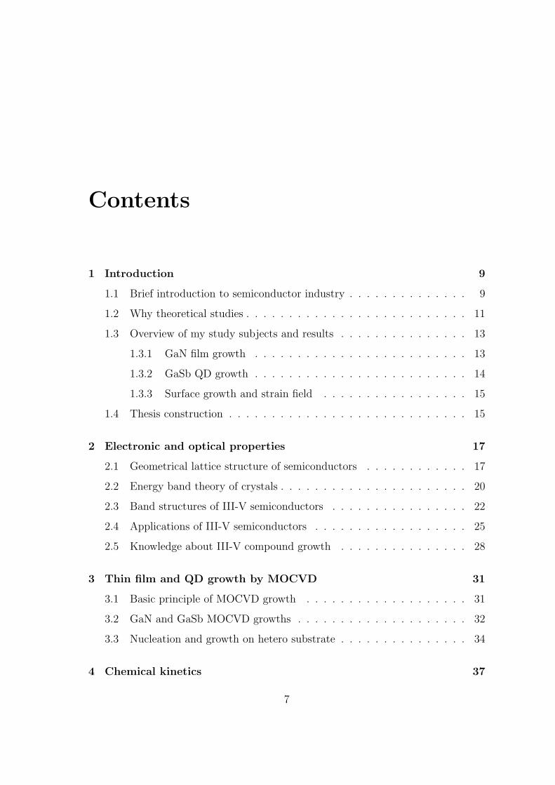
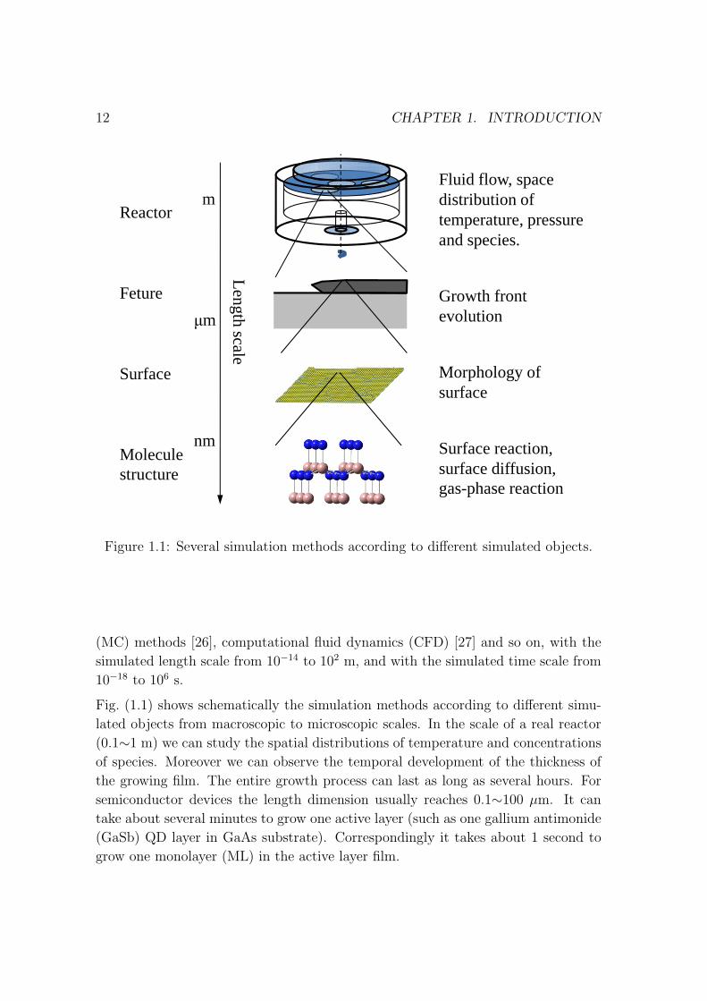
Figure 1.1: Several simulation methods according to different simulated objects.
(MC) methods [26], computational fluid dynamics (CFD) [27] and so on, with the
simulated length scale from 10−14 to 102 m, and with the simulated time scale from
10−18 to 106 s.
Fig. (1.1) shows schematically the simulation methods according to different simu-
lated objects from macroscopic to microscopic scales. In the scale of a real reactor
(0.1∼1 m) we can study the spatial distributions of temperature and concentrations
of species. Moreover we can observe the temporal development of the thickness of
the growing film. The entire growth process can last as long as several hours. For
semiconductor devices the length dimension usually reaches 0.1∼100 µm. It can
take about several minutes to grow one active layer (such as one gallium antimonide
(GaSb) QD layer in GaAs substrate). Correspondingly it takes about 1 second to
grow one monolayer (ML) in the active layer film.
1.3. OVERVIEW OF MY STUDY SUBJECTS AND RESULTS 13
[(CH3)2Ga:NH2]3
6CH4 + 3GaN
GaNH2
CH3+
Ga
+ NH3
CH3+
(CH3)2Ga
NH3 + (CH3)3Ga
(CH3)3Ga:NH3
CH4+
(CH3)2Ga:NH2
Lo
w R
ou
te(D
eco
mp
osi
tio
n)
Up
per
Ro
ute
(Ad
du
ct)
WAFER
CH3+
(CH3)Ga> 50% at 1000
GasGas--phase Nucleationphase Nucleation
+ CH+ CH33 or NHor NH22
Surface ReactionsSurface Reactions
+ CH+ CH33 or NHor NH22
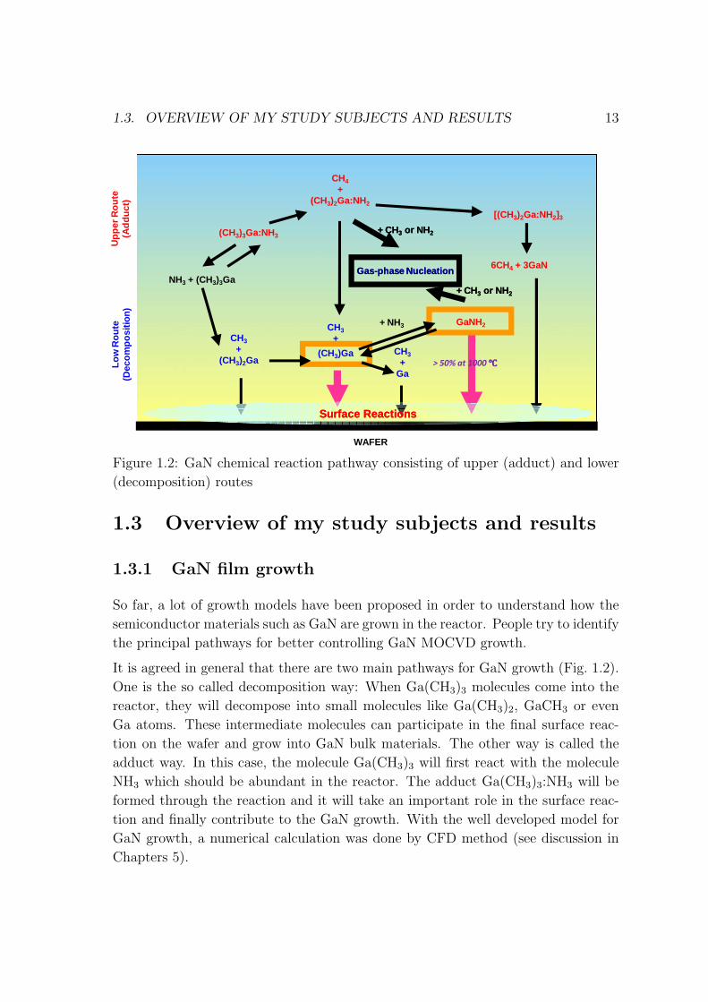
Figure 1.2: GaN chemical reaction pathway consisting of upper (adduct) and lower
(decomposition) routes
1.3 Overview of my study subjects and results
1.3.1 GaN film growth
So far, a lot of growth models have been proposed in order to understand how the
semiconductor materials such as GaN are grown in the reactor. People try to identify
the principal pathways for better controlling GaN MOCVD growth.
It is agreed in general that there are two main pathways for GaN growth (Fig. 1.2).
One is the so called decomposition way: When Ga(CH3)3 molecules come into the
reactor, they will decompose into small molecules like Ga(CH3)2, GaCH3 or even
Ga atoms. These intermediate molecules can participate in the final surface reac-
tion on the wafer and grow into GaN bulk materials. The other way is called the
adduct way. In this case, the molecule Ga(CH3)3 will first react with the molecule
NH3 which should be abundant in the reactor. The adduct Ga(CH3)3:NH3 will be
formed through the reaction and it will take an important role in the surface reac-
tion and finally contribute to the GaN growth. With the well developed model for
GaN growth, a numerical calculation was done by CFD method (see discussion in
Chapters 5).
14 CHAPTER 1. INTRODUCTION
1.3.2 GaSb QD growth
GaSb is used in a variety of electronic and optical device applications. It can be used
for infrared detectors, infrared LEDs and lasers and transistors, and thermophoto-
voltaic systems. [28] The growth of GaSb have been extensively explored by a large
number of groups. [29, 30, 31] GaSb was one of the first materials to be grown by
MOCVD. It is usually grown at relative low temperature (≤ 600 C) with a V/III
close to 1. The maximum growth temperature is limited by the low melting point of
GaSb (705 C [32]). The common growth precursors such as TMG ((CH3)3Ga) and
trimethylantimony (TMSb, (CH3)3Sb), is typically carried out over a range of tem-
peratures in order to kinetically limit the decomposition of these source molecules.
This kinetically-limited growth behavior results in a growth rate and materials prop-
erties that are particularly dependent on local substrate temperature variations. [33]
On the other hand, the too low or too high V/III ratio could result in the appearance
of elemental indium or antimony on the surface. It is because of the rather low vapor
pressure of Sb at typical MOCVD growth temperatures of 500 ∼ 700 C, which may
be only 1/6 as low as that of arsenic and phosphorus. [34] Thus V/III ratio should
be carefully controlled in order to avoid the formation of unexpected phases such
as gallium droplets or antimony hillocks. Specifically, the optimized V/III ratio for
the qualified GaSb growth depends on the reactor design, growth conditions, and
sources used. Among several sources used for the growth of GaSb, the most common
sources, such as TMG, triethylgallium (TEG), TMSb and triethylantimony (TESb),
give the most consistent results in terms of high mobility and photoluminescence.
[35]
The dominant group V growth sources for As- and P-based materials are their re-
spective hydrides. Antimony hydride (SbH3) is not suitable for use in MOCVD
because it is unstable at room temperature and reacts with storage vessels and reac-
tor manifolds. [35] Alternative metal-organic precursors, such as TMSb and triethyl
antimony, are therefore employed. [35, 36] However, the use of an organic source can
impact the purity of the resulting film which is a disadvantage. At present, it is be-
lieved that the pathway for GaSb MOCVD growth is through pyrolysis of precursors
such as TMG/TEG and TMSb. At the final step of gas phase reaction, the provided
radicals monomethylgallium/monoethylgallium (MMG/MEG) and monomethylan-
timony (MMSb) is ready for the surface reactions. [33]
1.4. THESIS CONSTRUCTION 15
1.3.3 Surface growth and strain field
The surface process during semiconductor materials is studied by kinetic Monte
Carlo (KMC) method. For the strain induced QD growth, the short-range valence-
force-field (VFF) approach is studied, developed and applied to calculate the local
strain energy. The growth of GaN film and GaSb QD is simulated by KMC method
(Chapters 4 and 6)
In a brief summary, I have studied the growth dynamics of semiconductor nanos-
trutures. The general strategy of the numerical study is: Spatial distributions of
temperature and concentrations of gas species are to be obtained from CFD calcu-
lations which are to be used in KMC to study the surface process on the wafer at
atomic levels. During the KMC simulation of nanostructure growth I have found
that the strain between the wafer and deposited materials is the key factor that
affects the growth mode and the shape of QDs.
1.4 Thesis construction
This thesis is organized in the following way: Chapter 2 introduces the unique
electronic and optical properties of semiconductor nanostructures based on which
builds the semiconductor industry. MOCVD growth method and three primary
growth modes of thin film are described in Chapter 3, while in chapter 4 I introduce
the chemical kinetics which is applied in my simulation to obtain reaction rates
which are directly coupled into CFD and MC simulations. The application of CFD
method is presented in Chapter 5 to simulate and understand the growth of the GaN
films. In chapter 6 I discuss three growth modes of materials on a hetero substrate
and the KMC method will be introduced and its application to film/QD growths
will be discussed.

16 CHAPTER 1. INTRODUCTION
Chapter 2
Electronic and optical properties
Nanostructures refer to the structures of sizes ranging from 0.1 to 100 nm. Nanos-
tructures, including clusters, semiconductor QDs, metal-insulator-metal structures
as well as semiconductor hetrostructures, have unique electromagnetic, optical and
chemical properties. Semiconductor nanostructures are the most promising materi-
als to be applied in the industry world and human’s daily life. The semiconductor
nanostructures are expected to be applied in the many fields of photocatalyst, op-
tical fiber communication, solar cells and sensors used for temperature, gases, light
as well as humidity.
At present, the development of semiconductor nanostructures is focused largely on
the following aspects. First, the study about universal laws of the properties of
nanostructures is being continued. Second, novel nano semiconductor compound
materials are under constant exploitation. Furthermore, for large scale applications
of products from the research laboratory to the industry world, it is required to
find methods of mass productions of semiconductor nanomaterials with precise size
control and clean surfaces.
2.1 Geometrical lattice structure of semiconduc-
tors
Semiconductor is a crystal material that has a resistivity value which is less than
the one of a conductor and more than an insulator. A crystal is defined by a regular
array of atoms/ions which repeat periodically in the space. Bravais lattice is used
to describe the lattice sites of atoms and can be defined as a regular periodic point
17
18 CHAPTER 2. ELECTRONIC AND OPTICAL PROPERTIES
x
y
z
a
R3
R2
R1
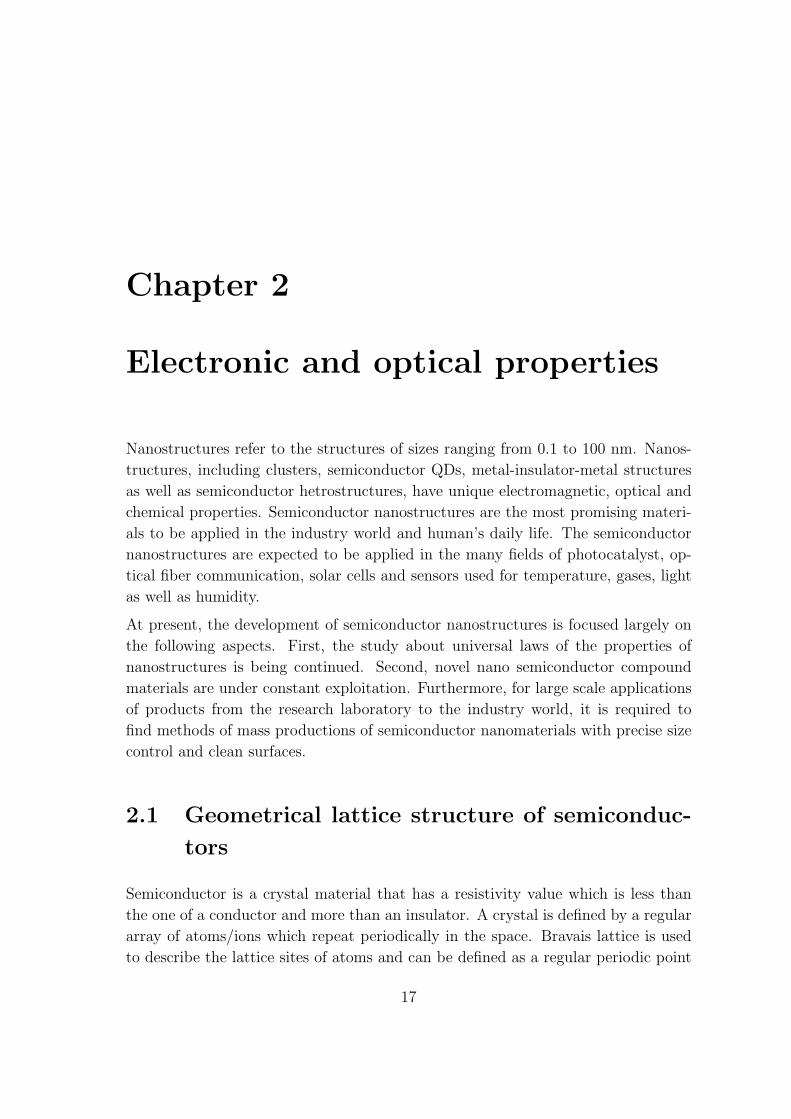
Figure 2.1: Face-centered cubic lattice and primitive translation vectors R1, R2, R3
given by Eq. (2.2)
position in the space:
Rn1,n2,n3 = n1R1 + n2R2 + n3R3 (2.1)
where n1, n2, n3 are integers, and vectors R1, R2, R3 are primitive vectors. The
parallelepiped formed by R1, R2, R3 is called primitive cell with the volume Ω =
R1 · (R2 × R3). It has been shown that there are totally 14 different kinds of
three-dimensional (3D) lattices. In my research study, I concentrate on two of
them, namely the wurtzite and zinc blende structures. Before introducing these two
kinds of crystal structures I first briefly describe the face-centered cubic (fcc) and
hexagonal closed-packed (hcp) lattice structures. Refer to Fig. 2.1, the primitive
vectors of the fcc Bravais lattice are [37]
R1 =a
2
(0, 1, 1
)R2 =
a
2
(1, 0, 1
)R3 =
a
2
(1, 1, 0
)(2.2)
where a is the lattice constant. In the fcc structure, each atom has 12 nearest
neighbors (which is called coordination number) and each nearest neighbour is at a
distance of (a/√
2) to the central atom. The volume of the primitive cell is Ω = a3/4
which is 1/4 of the volume of the conventional cubic cell.
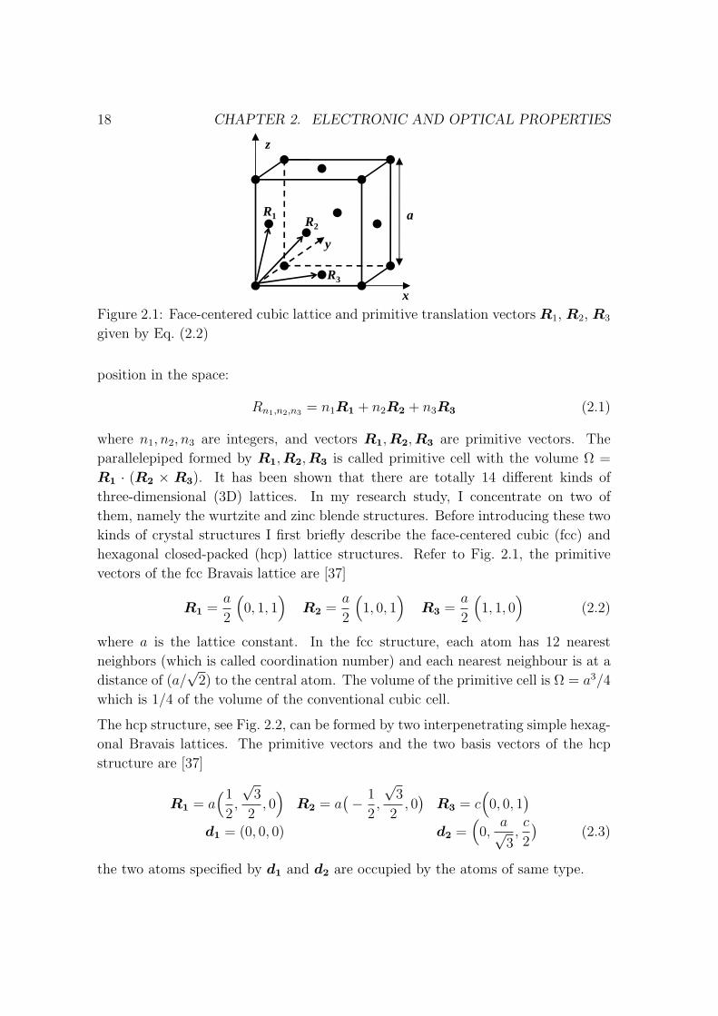
The hcp structure, see Fig. 2.2, can be formed by two interpenetrating simple hexag-
onal Bravais lattices. The primitive vectors and the two basis vectors of the hcp
structure are [37]
R1 = a(1
2,
√3
2, 0
)R2 = a
(− 1
2,
√3
2, 0
)R3 = c
(0, 0, 1
)
d1 = (0, 0, 0) d2 =(0,
a√3,c
2
)(2.3)
the two atoms specified by d1 and d2 are occupied by the atoms of same type.
2.1. GEOMETRICAL LATTICE STRUCTURE OF SEMICONDUCTORS 19
d1 R1
R2
d2
R3
xy
z
a
c
Figure 2.2: Crystal structure of hexagonal closed-packed lattice. The primitive
translation vectors R1, R2, R3 and the end points of vectors of the basis d1 and
d2 given in Eqs. (2.3) are shown.
x
y
z
a
d1
d2
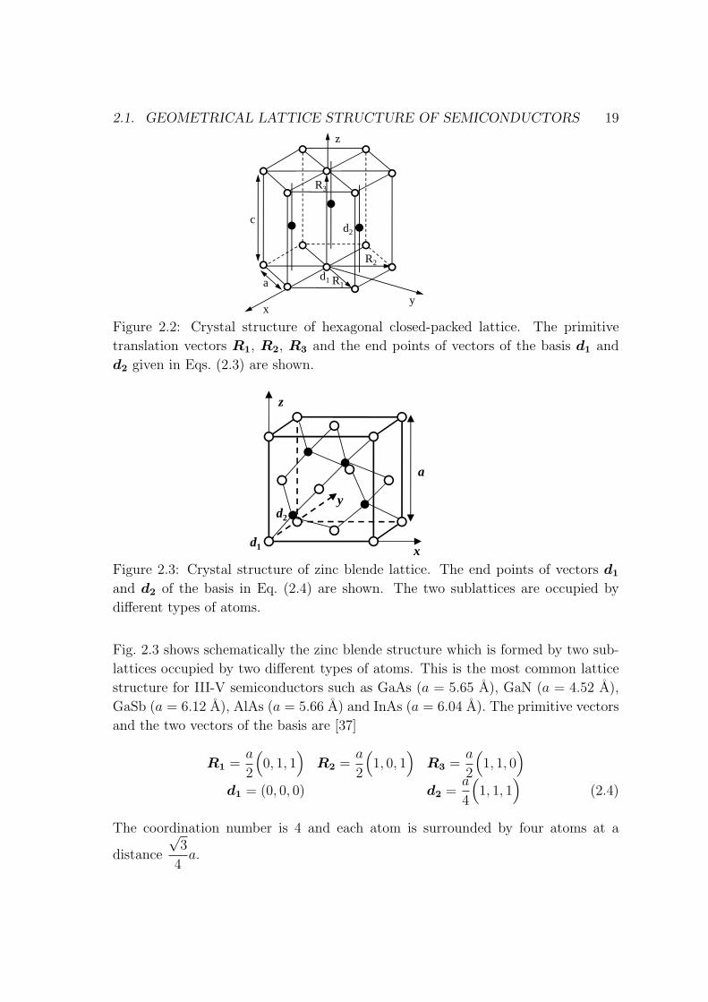
Figure 2.3: Crystal structure of zinc blende lattice. The end points of vectors d1
and d2 of the basis in Eq. (2.4) are shown. The two sublattices are occupied by
different types of atoms.
Fig. 2.3 shows schematically the zinc blende structure which is formed by two sub-
lattices occupied by two different types of atoms. This is the most common lattice
structure for III-V semiconductors such as GaAs (a = 5.65 A), GaN (a = 4.52 A),
GaSb (a = 6.12 A), AlAs (a = 5.66 A) and InAs (a = 6.04 A). The primitive vectors
and the two vectors of the basis are [37]
R1 =a
2
(0, 1, 1
)R2 =
a
2
(1, 0, 1
)R3 =
a
2
(1, 1, 0
)
d1 = (0, 0, 0) d2 =a
4
(1, 1, 1
)(2.4)
The coordination number is 4 and each atom is surrounded by four atoms at a
distance
√3
4a.
20 CHAPTER 2. ELECTRONIC AND OPTICAL PROPERTIES
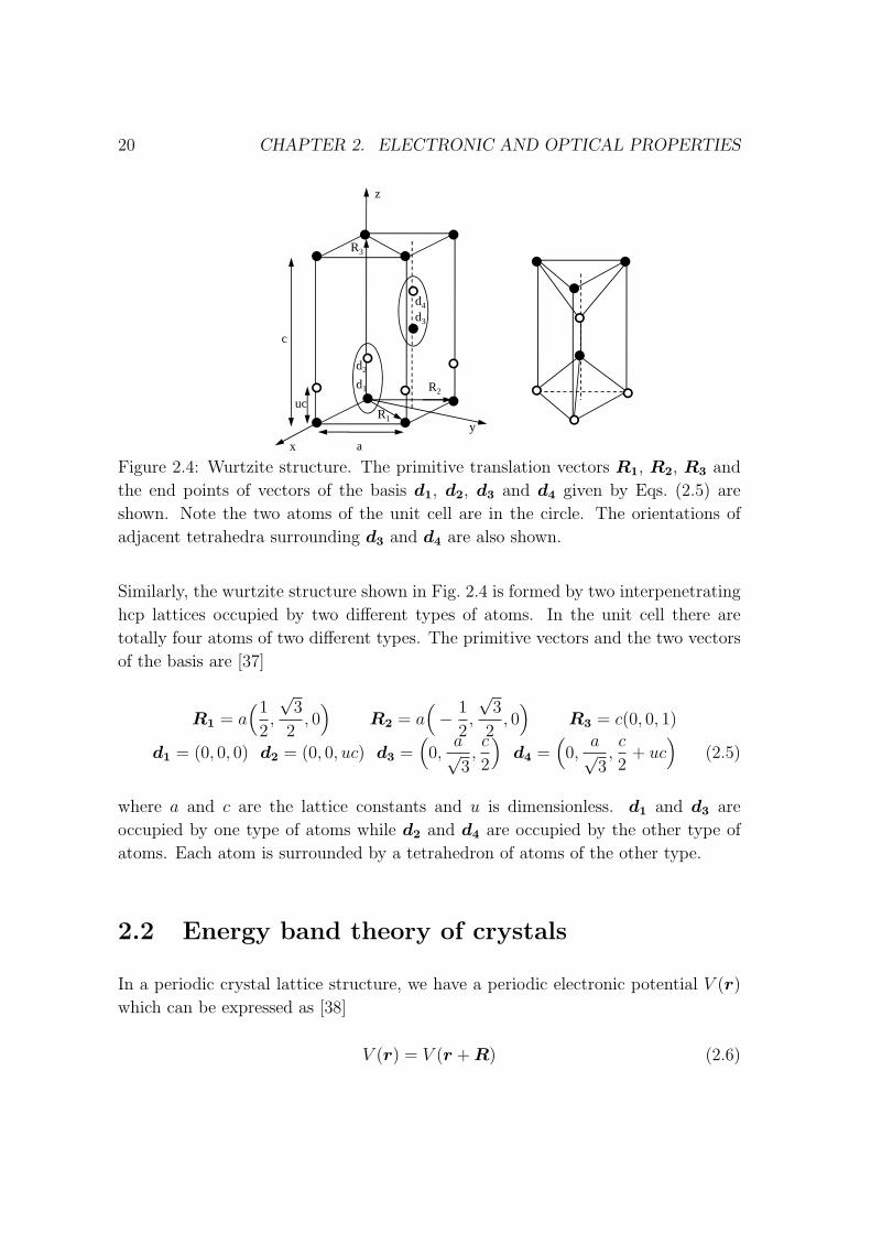
c
uc
R3
R2
R1
x
y
d2
d1
a
d4
d3
z
Figure 2.4: Wurtzite structure. The primitive translation vectors R1, R2, R3 and
the end points of vectors of the basis d1, d2, d3 and d4 given by Eqs. (2.5) are
shown. Note the two atoms of the unit cell are in the circle. The orientations of
adjacent tetrahedra surrounding d3 and d4 are also shown.
Similarly, the wurtzite structure shown in Fig. 2.4 is formed by two interpenetrating
hcp lattices occupied by two different types of atoms. In the unit cell there are
totally four atoms of two different types. The primitive vectors and the two vectors
of the basis are [37]
R1 = a(1
2,
√3
2, 0
)R2 = a
(− 1
2,
√3
2, 0
)R3 = c(0, 0, 1)
d1 = (0, 0, 0) d2 = (0, 0, uc) d3 =(0,
a√3,c
2
)d4 =
(0,
a√3,c
2+ uc
)(2.5)
where a and c are the lattice constants and u is dimensionless. d1 and d3 are
occupied by one type of atoms while d2 and d4 are occupied by the other type of
atoms. Each atom is surrounded by a tetrahedron of atoms of the other type.
2.2 Energy band theory of crystals
In a periodic crystal lattice structure, we have a periodic electronic potential V (r)
which can be expressed as [38]
V (r) = V (r + R) (2.6)
2.2. ENERGY BAND THEORY OF CRYSTALS 21
where R is an arbitrary lattice vector. One can write down the Schrodinger equation
for the electrons in such a periodic lattice structure as
[− ~2
2m0
∇2 + V (r)
]Ψ(r) = EΨ(r) (2.7)
where m0 is the mass of the free electron. Because of the periodicity of V (r), the
electron wave function has the following form
Ψnk(r) =1√N
unk(r)eik·r
unk(r) = unk(r + R) (2.8)
which is normally referred as the Bloch theorem. Here N = NxNyNz, Nx, Ny and
Nz are the number of unit cells along x, y and z direction, respectively. k is called
the electron wave vector and unk the periodic Bloch function.
The states of valence electrons in the isolated atoms are modified when the atoms
form a crystal. However we may express the wave functions of electrons in the
crystal by a linear combination of atomic orbitals, which is also the basis for the
tight-binding method [39, 40]. In this approach, we assume that the wave functions
of the electrons of the crystal atoms are very similar to the ones of the isolated
atom in free space. Interactions between different atomic sites are considered as
perturbations. There exist several kinds of interactions we must consider. The easy
way is that we only consider the interactions between the nearest neighbors. Most
compound semiconductor materials have zinc blende structures which have a cation-
anion pair occupying each lattice site. Moreover, for many semiconductor materials,
the electrons in the outmost shell can usually be described by s, px, py and pz types
of wave functions, i.e., totally four atomic orbitals. As mentioned before there are
usually two different kinds of atoms in each unit cell. The Bloch wave function is
written as
Ψ(r) =∑Ri
4∑m=1
2∑j=1
Cmj(k)Ψmj(r − rj −Ri)eik·Ri (2.9)
where Ri includes all of the unit cells, j = 1, 2 refer to the different atoms in the
unit cell and m corresponds to the 4 different atomic orbitals. By solving the secular
equation
|〈Ψm′j′|H − E|Ψ(k, r)〉| = 0 (2.10)
the energy band structure can be calculated for different values of k, which is nor-
mally referred to as the energy dispersion E = E(k). In addition to the tight-binding
22 CHAPTER 2. ELECTRONIC AND OPTICAL PROPERTIES
kz
AS
H
P
kx
kyK
M
T´
S´LR
T U
ΣΓ
∆
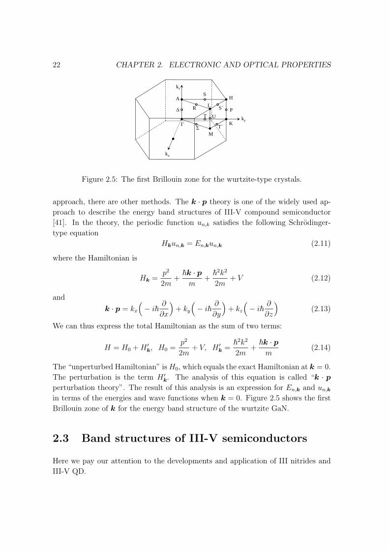
Figure 2.5: The first Brillouin zone for the wurtzite-type crystals.
approach, there are other methods. The k · p theory is one of the widely used ap-
proach to describe the energy band structures of III-V compound semiconductor
[41]. In the theory, the periodic function un,k satisfies the following Schrodinger-
type equation
Hkun,k = En,kun,k (2.11)
where the Hamiltonian is
Hk =p2
2m+~k · p
m+~2k2
2m+ V (2.12)
and
k · p = kx
(− i~
∂
∂x
)+ ky
(− i~
∂
∂y
)+ kz
(− i~
∂
∂z
)(2.13)
We can thus express the total Hamiltonian as the sum of two terms:
H = H0 + H ′k, H0 =
p2
2m+ V, H ′
k =~2k2
2m+~k · p
m(2.14)
The “unperturbed Hamiltonian” is H0, which equals the exact Hamiltonian at k = 0.
The perturbation is the term H ′k. The analysis of this equation is called “k · p
perturbation theory”. The result of this analysis is an expression for En,k and un,k
in terms of the energies and wave functions when k = 0. Figure 2.5 shows the first
Brillouin zone of k for the energy band structure of the wurtzite GaN.
2.3 Band structures of III-V semiconductors
Here we pay our attention to the developments and application of III nitrides and
III-V QD.
2.3. BAND STRUCTURES OF III-V SEMICONDUCTORS 23
Split-off band
Γ1c
Γ9v Eso
Ecrkz kx
Energy
A-valleyM-L-valleys
Γ-valley
EM-LEAEg
Heavy holesLight holes
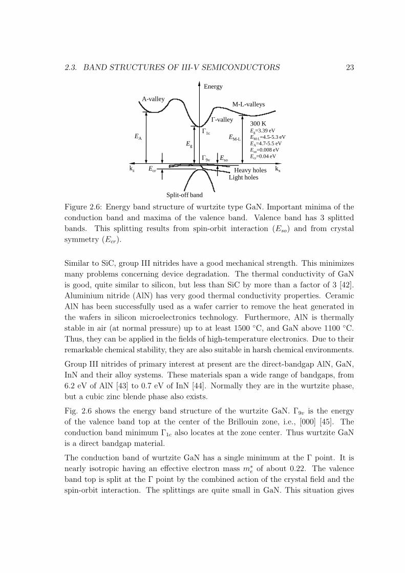
300 KEg=3.39 eVEM-L=4.5-5.3 eVEA=4.7-5.5 eVEso=0.008 eVEcr=0.04 eV
Figure 2.6: Energy band structure of wurtzite type GaN. Important minima of the
conduction band and maxima of the valence band. Valence band has 3 splitted
bands. This splitting results from spin-orbit interaction (Eso) and from crystal
symmetry (Ecr).
Similar to SiC, group III nitrides have a good mechanical strength. This minimizes
many problems concerning device degradation. The thermal conductivity of GaN
is good, quite similar to silicon, but less than SiC by more than a factor of 3 [42].
Aluminium nitride (AlN) has very good thermal conductivity properties. Ceramic
AlN has been successfully used as a wafer carrier to remove the heat generated in
the wafers in silicon microelectronics technology. Furthermore, AlN is thermally
stable in air (at normal pressure) up to at least 1500 C, and GaN above 1100 C.
Thus, they can be applied in the fields of high-temperature electronics. Due to their
remarkable chemical stability, they are also suitable in harsh chemical environments.
Group III nitrides of primary interest at present are the direct-bandgap AlN, GaN,
InN and their alloy systems. These materials span a wide range of bandgaps, from
6.2 eV of AlN [43] to 0.7 eV of InN [44]. Normally they are in the wurtzite phase,
but a cubic zinc blende phase also exists.
Fig. 2.6 shows the energy band structure of the wurtzite GaN. Γ9v is the energy
of the valence band top at the center of the Brillouin zone, i.e., [000] [45]. The
conduction band minimum Γ1c also locates at the zone center. Thus wurtzite GaN
is a direct bandgap material.
The conduction band of wurtzite GaN has a single minimum at the Γ point. It is
nearly isotropic having an effective electron mass m∗e of about 0.22. The valence
band top is split at the Γ point by the combined action of the crystal field and the
spin-orbit interaction. The splittings are quite small in GaN. This situation gives
24 CHAPTER 2. ELECTRONIC AND OPTICAL PROPERTIES
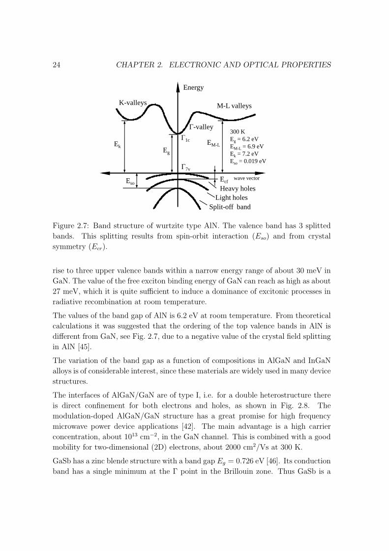
Energy
M-L valleys
Γ-valley
K-valleys
EkEg
EM-L
EcfEsowave vector
Light holesHeavy holes
Split-off band
300 KEg = 6.2 eVEM-L = 6.9 eVEk = 7.2 eVEso = 0.019 eV
Γ7v
Γ1c
Figure 2.7: Band structure of wurtzite type AlN. The valence band has 3 splitted
bands. This splitting results from spin-orbit interaction (Eso) and from crystal
symmetry (Ecr).
rise to three upper valence bands within a narrow energy range of about 30 meV in
GaN. The value of the free exciton binding energy of GaN can reach as high as about
27 meV, which it is quite sufficient to induce a dominance of excitonic processes in
radiative recombination at room temperature.
The values of the band gap of AlN is 6.2 eV at room temperature. From theoretical
calculations it was suggested that the ordering of the top valence bands in AlN is
different from GaN, see Fig. 2.7, due to a negative value of the crystal field splitting
in AlN [45].
The variation of the band gap as a function of compositions in AlGaN and InGaN
alloys is of considerable interest, since these materials are widely used in many device
structures.
The interfaces of AlGaN/GaN are of type I, i.e. for a double heterostructure there
is direct confinement for both electrons and holes, as shown in Fig. 2.8. The
modulation-doped AlGaN/GaN structure has a great promise for high frequency
microwave power device applications [42]. The main advantage is a high carrier
concentration, about 1013 cm−2, in the GaN channel. This is combined with a good
mobility for two-dimensional (2D) electrons, about 2000 cm2/Vs at 300 K.
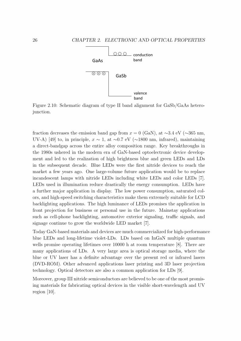
GaSb has a zinc blende structure with a band gap Eg = 0.726 eV [46]. Its conduction
band has a single minimum at the Γ point in the Brillouin zone. Thus GaSb is a
2.4. APPLICATIONS OF III-V SEMICONDUCTORS 25
AlGaN GaN
conduction
band
valence
band
+ + +
- - -
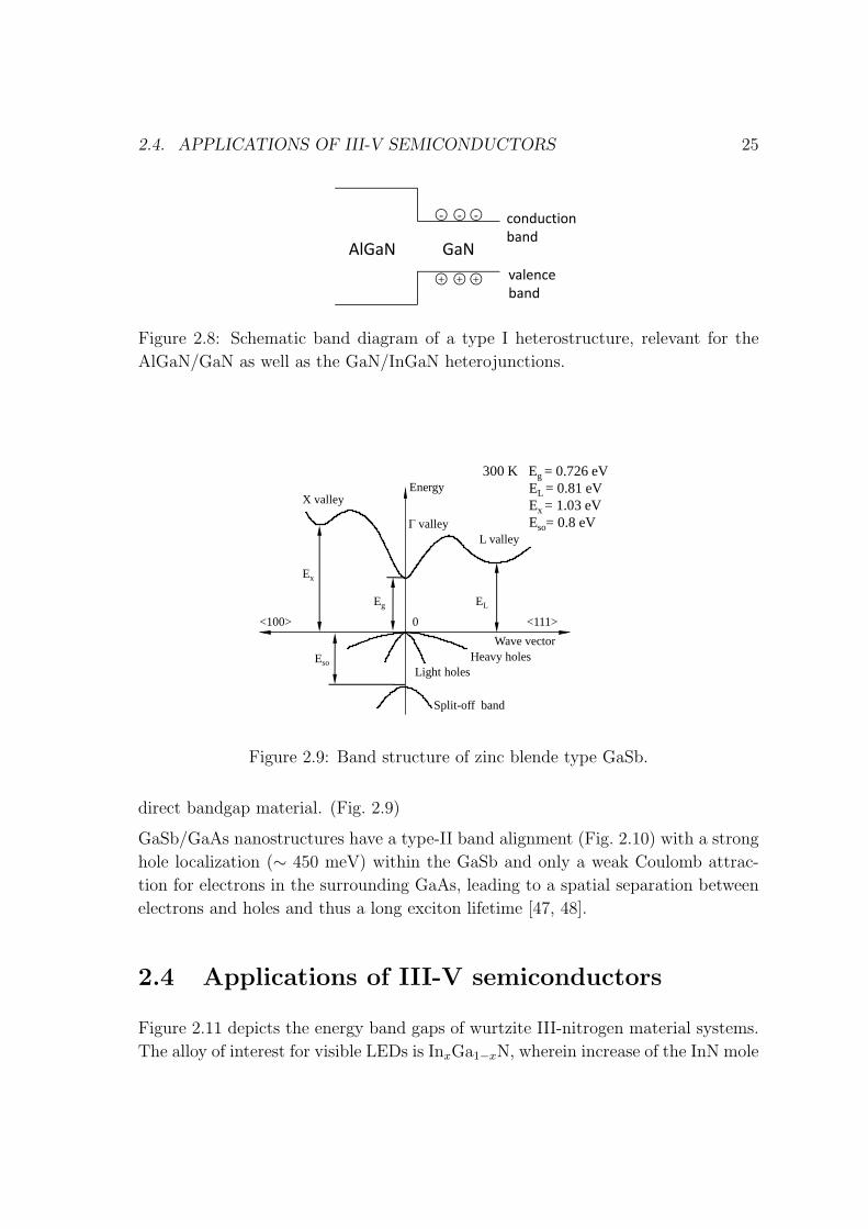
Figure 2.8: Schematic band diagram of a type I heterostructure, relevant for the
AlGaN/GaN as well as the GaN/InGaN heterojunctions.
Energy
<111><100>
Ex
Eg EL
0
Eso
X valley
Γ valleyL valley
Heavy holesLight holes
300 K Eg = 0.726 eVEL = 0.81 eVEx = 1.03 eVEso= 0.8 eV
Wave vector
Split-off band
Figure 2.9: Band structure of zinc blende type GaSb.
direct bandgap material. (Fig. 2.9)
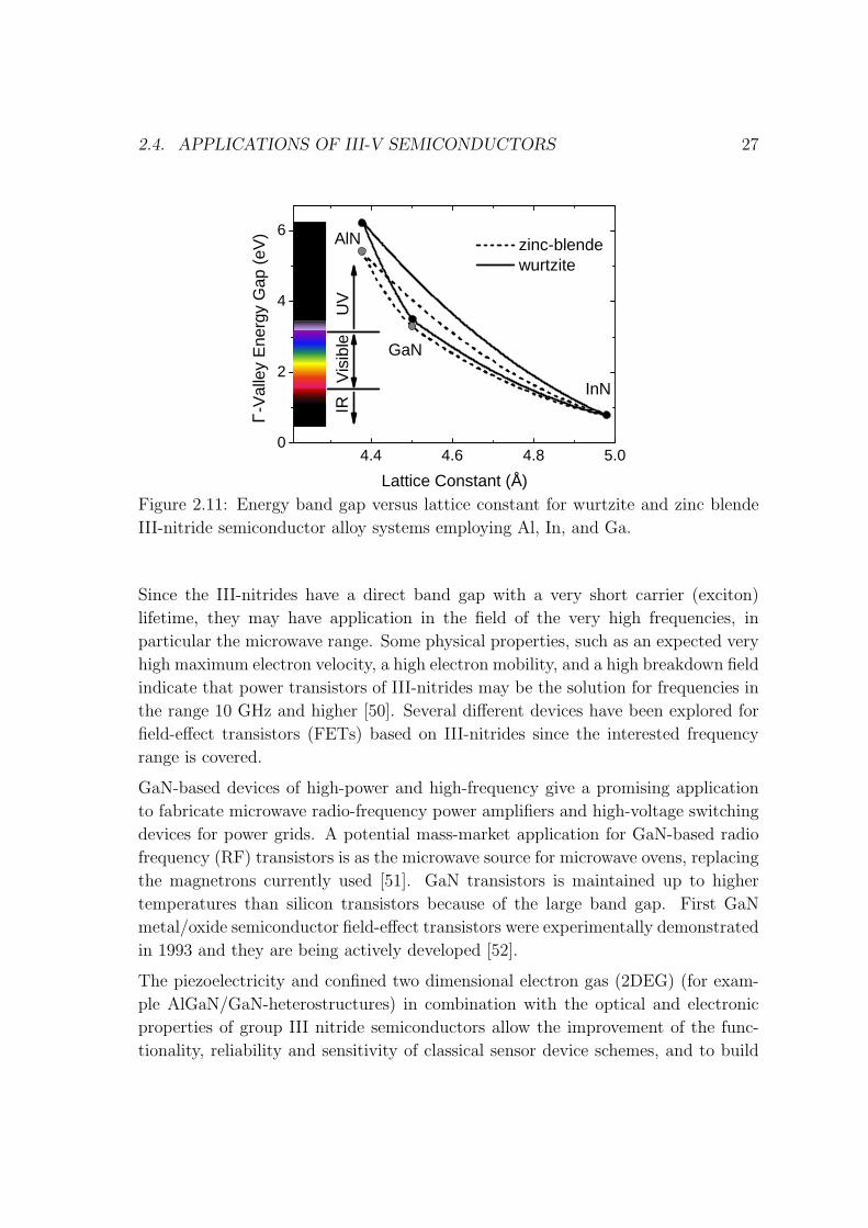
GaSb/GaAs nanostructures have a type-II band alignment (Fig. 2.10) with a strong
hole localization (∼ 450 meV) within the GaSb and only a weak Coulomb attrac-
tion for electrons in the surrounding GaAs, leading to a spatial separation between
electrons and holes and thus a long exciton lifetime [47, 48].
2.4 Applications of III-V semiconductors
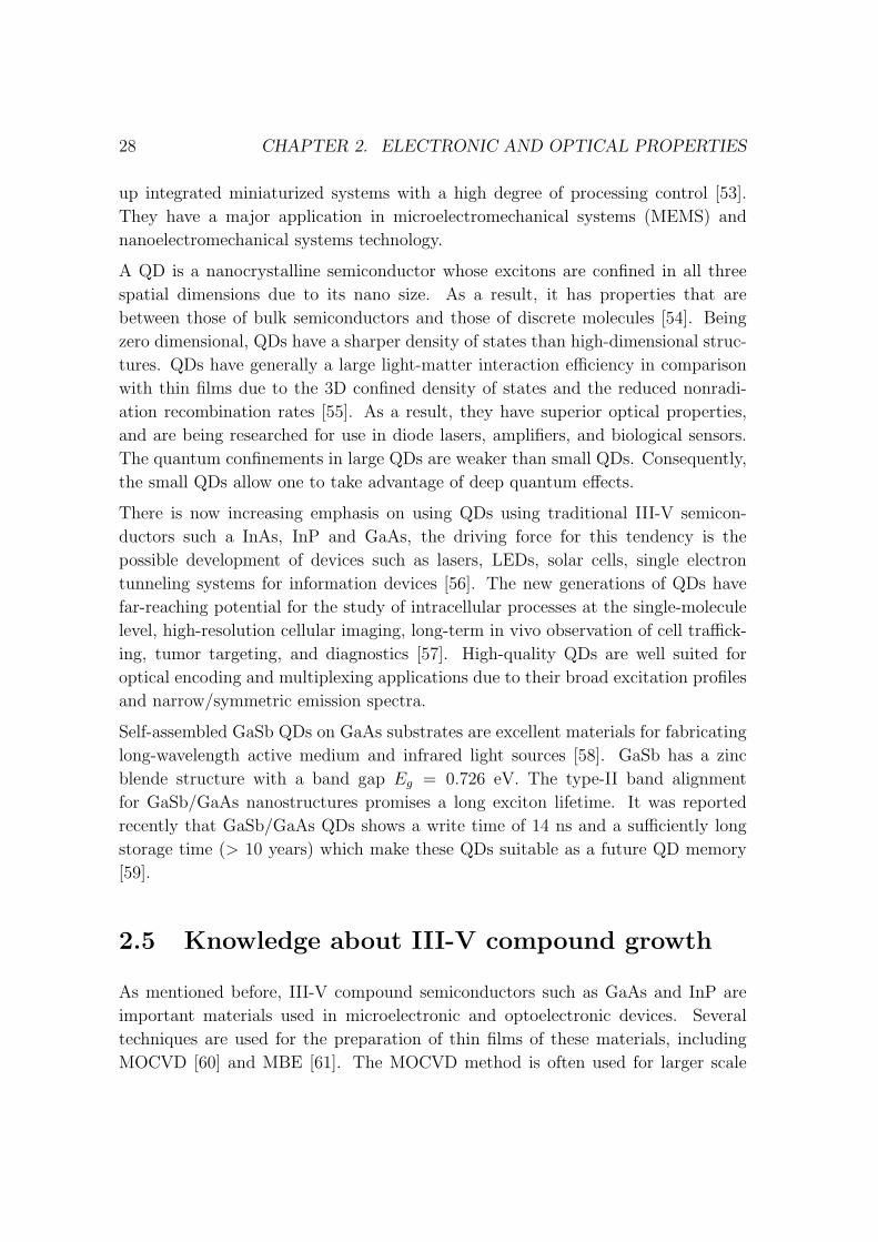
Figure 2.11 depicts the energy band gaps of wurtzite III-nitrogen material systems.
The alloy of interest for visible LEDs is InxGa1−xN, wherein increase of the InN mole
26 CHAPTER 2. ELECTRONIC AND OPTICAL PROPERTIES
conduction
band
valence
band
GaAs
GaSb+++
— ——
Figure 2.10: Schematic diagram of type II band alignment for GaSb/GaAs hetero-
junction.
fraction decreases the emission band gap from x = 0 (GaN), at ∼3.4 eV (∼365 nm,
UV-A) [49] to, in principle, x ∼ 1, at ∼0.7 eV (∼1800 nm, infrared), maintaining
a direct-bandgap across the entire alloy composition range. Key breakthroughs in
the 1980s ushered in the modern era of GaN-based optoelectronic device develop-
ment and led to the realization of high brightness blue and green LEDs and LDs
in the subsequent decade. Blue LEDs were the first nitride devices to reach the
market a few years ago. One large-volume future application would be to replace
incandescent lamps with nitride LEDs including white LEDs and color LEDs [7].
LEDs used in illumination reduce drastically the energy consumption. LEDs have
a further major application in display. The low power consumption, saturated col-
ors, and high-speed switching characteristics make them extremely suitable for LCD
backlighting applications. The high luminance of LEDs promises the application in
front projection for business or personal use in the future. Mainstay applications
such as cell-phone backlighting, automotive exterior signaling, traffic signals, and
signage continue to grow the worldwide LED market [7].
Today GaN-based materials and devices are much commercialized for high-performance
blue LEDs and long-lifetime violet-LDs. LDs based on InGaN multiple quantum
wells promise operating lifetimes over 10000 h at room temperature [8]. There are
many applications of LDs. A very large area is optical storage media, where the
blue or UV laser has a definite advantage over the present red or infrared lasers
(DVD-ROM). Other advanced applications laser printing and 3D laser projection
technology. Optical detectors are also a common application for LDs [9].
Moreover, group III nitride semiconductors are believed to be one of the most promis-
ing materials for fabricating optical devices in the visible short-wavelength and UV
region [10].
2.4. APPLICATIONS OF III-V SEMICONDUCTORS 27
4.4 4.6 4.8 5.00
2
4
6
Vis
ible
UV
AlN
InN
Lattice Constant (Å)
zinc-blende wurtzite
Γ-V
alle
y E
nerg
y G
ap (
eV)
GaNIR
Figure 2.11: Energy band gap versus lattice constant for wurtzite and zinc blende
III-nitride semiconductor alloy systems employing Al, In, and Ga.
Since the III-nitrides have a direct band gap with a very short carrier (exciton)
lifetime, they may have application in the field of the very high frequencies, in
particular the microwave range. Some physical properties, such as an expected very
high maximum electron velocity, a high electron mobility, and a high breakdown field
indicate that power transistors of III-nitrides may be the solution for frequencies in
the range 10 GHz and higher [50]. Several different devices have been explored for
field-effect transistors (FETs) based on III-nitrides since the interested frequency
range is covered.
GaN-based devices of high-power and high-frequency give a promising application
to fabricate microwave radio-frequency power amplifiers and high-voltage switching
devices for power grids. A potential mass-market application for GaN-based radio
frequency (RF) transistors is as the microwave source for microwave ovens, replacing
the magnetrons currently used [51]. GaN transistors is maintained up to higher
temperatures than silicon transistors because of the large band gap. First GaN
metal/oxide semiconductor field-effect transistors were experimentally demonstrated
in 1993 and they are being actively developed [52].
The piezoelectricity and confined two dimensional electron gas (2DEG) (for exam-
ple AlGaN/GaN-heterostructures) in combination with the optical and electronic
properties of group III nitride semiconductors allow the improvement of the func-
tionality, reliability and sensitivity of classical sensor device schemes, and to build
28 CHAPTER 2. ELECTRONIC AND OPTICAL PROPERTIES
up integrated miniaturized systems with a high degree of processing control [53].
They have a major application in microelectromechanical systems (MEMS) and
nanoelectromechanical systems technology.
A QD is a nanocrystalline semiconductor whose excitons are confined in all three
spatial dimensions due to its nano size. As a result, it has properties that are
between those of bulk semiconductors and those of discrete molecules [54]. Being
zero dimensional, QDs have a sharper density of states than high-dimensional struc-
tures. QDs have generally a large light-matter interaction efficiency in comparison
with thin films due to the 3D confined density of states and the reduced nonradi-
ation recombination rates [55]. As a result, they have superior optical properties,
and are being researched for use in diode lasers, amplifiers, and biological sensors.
The quantum confinements in large QDs are weaker than small QDs. Consequently,
the small QDs allow one to take advantage of deep quantum effects.
There is now increasing emphasis on using QDs using traditional III-V semicon-
ductors such a InAs, InP and GaAs, the driving force for this tendency is the
possible development of devices such as lasers, LEDs, solar cells, single electron
tunneling systems for information devices [56]. The new generations of QDs have
far-reaching potential for the study of intracellular processes at the single-molecule
level, high-resolution cellular imaging, long-term in vivo observation of cell traffick-
ing, tumor targeting, and diagnostics [57]. High-quality QDs are well suited for
optical encoding and multiplexing applications due to their broad excitation profiles
and narrow/symmetric emission spectra.
Self-assembled GaSb QDs on GaAs substrates are excellent materials for fabricating
long-wavelength active medium and infrared light sources [58]. GaSb has a zinc
blende structure with a band gap Eg = 0.726 eV. The type-II band alignment
for GaSb/GaAs nanostructures promises a long exciton lifetime. It was reported
recently that GaSb/GaAs QDs shows a write time of 14 ns and a sufficiently long
storage time (> 10 years) which make these QDs suitable as a future QD memory
[59].
2.5 Knowledge about III-V compound growth
As mentioned before, III-V compound semiconductors such as GaAs and InP are
important materials used in microelectronic and optoelectronic devices. Several
techniques are used for the preparation of thin films of these materials, including
MOCVD [60] and MBE [61]. The MOCVD method is often used for larger scale
2.5. KNOWLEDGE ABOUT III-V COMPOUND GROWTH 29
processes and widely applied in the industry. The typical reaction in MOCVD
process involves a group III trialkyl such as TMG, with AsH3 or PH3 at adequate
temperature (∼ 700 C)
TMG + AsH3 −→ GaAs + 3CH4 (2.15)
However, the conventional MOCVD could bring many kinds of troubles such as po-
tential environmental, safety, and health hazards of handling pyrophoric and toxic
reagents under these conditions. It also suffers from stoichiometry control problems,
impurity incorporation and un-desired side reactions. Moreover, the high tempera-
tures involved can promote interdiffusion of atomic layers which could prevent sharp
heterojunctions from being achieved. Attempts to grow superior films by modifica-
tions of the MOCVD process include low-pressure MOCVD [62], plasma-enhanced
MOCVD [63], and hybrid MBE MOCVD systems [64].
Theoretical studies have been performed about the reaction mechanisms of GaN
films based on CFD simulation [65, 66, 67], where activation energy barriers of
the gas-phase reactions and the surface reaction steps were calculated using quan-
tum chemistry methods [68, 69]. MMG (GaCH3), MMG:NH3 (GaCH3:NH3) and
TMG:NH3 (Ga(CH3)3:NH3) were assumed by Sengupta to be the principal radicals
in the gas phase for GaN film growth, which were the intermediate products during
the gas-phase reactions in the MOCVD reactor [65]. Mihopoulos et al. assumed
however that the principal radicals are “Ga-N” pseudo molecules in the vicinity of
the film surface [66]. It was further proposed that a Ga-containing molecular struc-
ture for a stable gas-phase GaN cyclic adduct was the major resource for Ga species
during the GaN gas-phase growth process [67]. Recently, Kusakabe et al. [70] and
Hirako et al. [71] combined the two models of Ref. [65, 66] in their CFD simulations
in order to further understand the growth dynamics of GaN films. All these works
include mostly the gas-phase reactions and the intermediate products in the gas
phase during the growth (see Fig. 1.2). Further works have added surface reactions
[27, 65, 72, 73, 74, 75].

30 CHAPTER 2. ELECTRONIC AND OPTICAL PROPERTIES
Chapter 3
Thin film and QD growth by
MOCVD
Metalorganic chemical vapour deposition (MOCVD) is a chemical vapour deposi-
tion method of epitaxial growth of materials, especially compound semiconductors.
Usually one of the reaction species containing the required chemical elements is an
organic compound or metal-organics and metal hydrides, which has a low boiling
temperature. Formation of the epitaxial layer occurs by final pyrolysis of the con-
stituent chemicals at the substrate surface. The semiconductor’s growth takes place
not in a vacuum but with gas in the reactor at a moderate pressure (2 ∼ 100 kPa).
The III-V semiconductors (InN, GaN, GaAs etc), II-VI semiconductors (HgCdTe,
ZnO), IV semiconductors (SiC, SiGe) are usually grown by MOCVD. Today it has
become the dominant process for the manufacture of LDs, solar cells, and LEDs in
the industry world.
3.1 Basic principle of MOCVD growth
Today’s MOCVD GaN growth reactor was developed from the approach of Maruska
and Tietjen, which is capable of depositing films with AlN and InN [76]. Usually
there are two types of reactors, one is horizontal, Fig. 3.1(a), and the other vertical,
Fig. 3.1(b). For the horizontal reactor, the gas precursors blow into the reactor from
the left side, and the materials are deposited on the substrate in the middle of the
reactor. Usually the substrate has an inclination with respect to the horizontal flow
direction of input gases in order to make uniform semiconductor films with favorable
crystallinity. In the vertical reactor the precursors are blown into the reactor from
31
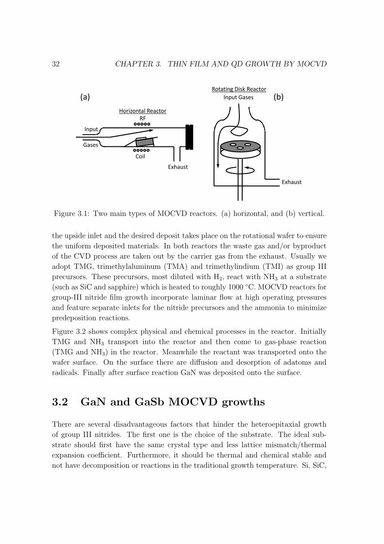
32 CHAPTER 3. THIN FILM AND QD GROWTH BY MOCVD
Horizontal Reactor
RF
Input
Gases
Coil
Exhaust
Rotating Disk Reactor
Input Gases
Exhaust
(a) (b)
Figure 3.1: Two main types of MOCVD reactors. (a) horizontal, and (b) vertical.
the upside inlet and the desired deposit takes place on the rotational wafer to ensure
the uniform deposited materials. In both reactors the waste gas and/or byproduct
of the CVD process are taken out by the carrier gas from the exhaust. Usually we
adopt TMG, trimethylaluminum (TMA) and trimethylindium (TMI) as group III
precursors. These precursors, most diluted with H2, react with NH3 at a substrate
(such as SiC and sapphire) which is heated to roughly 1000 C. MOCVD reactors for
group-III nitride film growth incorporate laminar flow at high operating pressures
and feature separate inlets for the nitride precursors and the ammonia to minimize
predeposition reactions.
Figure 3.2 shows complex physical and chemical processes in the reactor. Initially
TMG and NH3 transport into the reactor and then come to gas-phase reaction
(TMG and NH3) in the reactor. Meanwhile the reactant was transported onto the
wafer surface. On the surface there are diffusion and desorption of adatoms and
radicals. Finally after surface reaction GaN was deposited onto the surface.
3.2 GaN and GaSb MOCVD growths
There are several disadvantageous factors that hinder the heteroepitaxial growth
of group III nitrides. The first one is the choice of the substrate. The ideal sub-
strate should first have the same crystal type and less lattice mismatch/thermal
expansion coefficient. Furthermore, it should be thermal and chemical stable and
not have decomposition or reactions in the traditional growth temperature. Si, SiC,
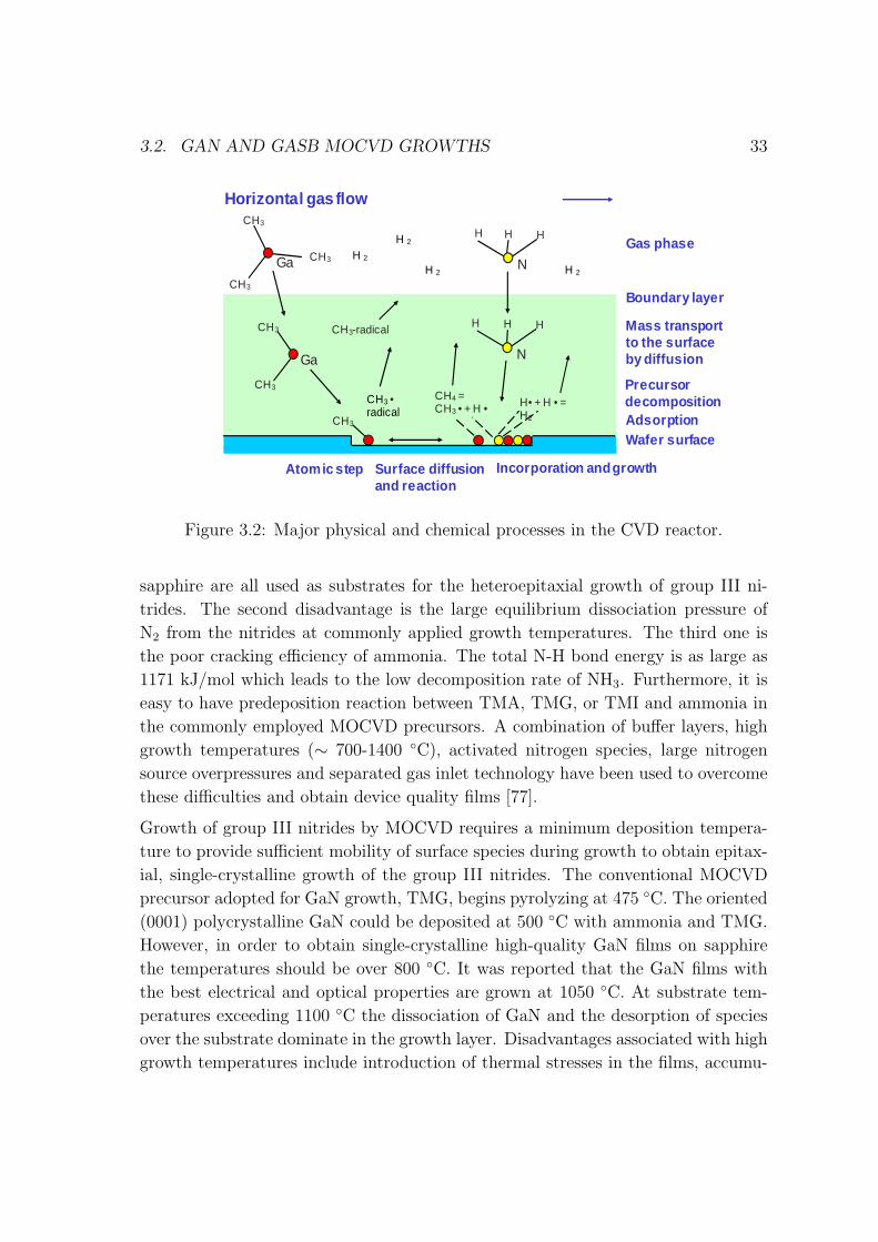
3.2. GAN AND GASB MOCVD GROWTHS 33
Boundary layer
Surface diffusionand reaction
Incorporation and growth
CH4 =CH3 • + H • H• + H • =
H2
Wafer surface
Mass transportto the surface by diffusion
Atomic step
HHH
N
CH3
Ga
CH3
CH3
Precursor decomposition
-radical
AdsorptionCH3
CH3 •radical
Gas phase
Horizontal gas flow
HHH
NGa CH3
CH3
CH3
H 2
H 2
H 2H 2
Figure 3.2: Major physical and chemical processes in the CVD reactor.
sapphire are all used as substrates for the heteroepitaxial growth of group III ni-
trides. The second disadvantage is the large equilibrium dissociation pressure of
N2 from the nitrides at commonly applied growth temperatures. The third one is
the poor cracking efficiency of ammonia. The total N-H bond energy is as large as
1171 kJ/mol which leads to the low decomposition rate of NH3. Furthermore, it is
easy to have predeposition reaction between TMA, TMG, or TMI and ammonia in
the commonly employed MOCVD precursors. A combination of buffer layers, high
growth temperatures (∼ 700-1400 C), activated nitrogen species, large nitrogen
source overpressures and separated gas inlet technology have been used to overcome
these difficulties and obtain device quality films [77].
Growth of group III nitrides by MOCVD requires a minimum deposition tempera-
ture to provide sufficient mobility of surface species during growth to obtain epitax-
ial, single-crystalline growth of the group III nitrides. The conventional MOCVD
precursor adopted for GaN growth, TMG, begins pyrolyzing at 475 C. The oriented
(0001) polycrystalline GaN could be deposited at 500 C with ammonia and TMG.
However, in order to obtain single-crystalline high-quality GaN films on sapphire
the temperatures should be over 800 C. It was reported that the GaN films with
the best electrical and optical properties are grown at 1050 C. At substrate tem-
peratures exceeding 1100 C the dissociation of GaN and the desorption of species
over the substrate dominate in the growth layer. Disadvantages associated with high
growth temperatures include introduction of thermal stresses in the films, accumu-
34 CHAPTER 3. THIN FILM AND QD GROWTH BY MOCVD
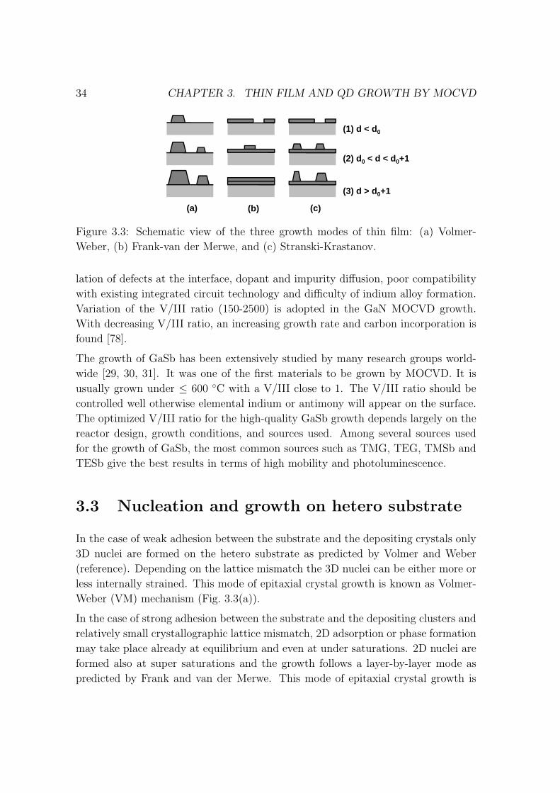
(a) (b) (c)
(2) d0 < d < d0+1
(3) d > d0+1
(1) d < d0
Figure 3.3: Schematic view of the three growth modes of thin film: (a) Volmer-
Weber, (b) Frank-van der Merwe, and (c) Stranski-Krastanov.
lation of defects at the interface, dopant and impurity diffusion, poor compatibility
with existing integrated circuit technology and difficulty of indium alloy formation.
Variation of the V/III ratio (150-2500) is adopted in the GaN MOCVD growth.
With decreasing V/III ratio, an increasing growth rate and carbon incorporation is
found [78].
The growth of GaSb has been extensively studied by many research groups world-
wide [29, 30, 31]. It was one of the first materials to be grown by MOCVD. It is
usually grown under ≤ 600 C with a V/III close to 1. The V/III ratio should be
controlled well otherwise elemental indium or antimony will appear on the surface.
The optimized V/III ratio for the high-quality GaSb growth depends largely on the
reactor design, growth conditions, and sources used. Among several sources used
for the growth of GaSb, the most common sources such as TMG, TEG, TMSb and
TESb give the best results in terms of high mobility and photoluminescence.
3.3 Nucleation and growth on hetero substrate
In the case of weak adhesion between the substrate and the depositing crystals only
3D nuclei are formed on the hetero substrate as predicted by Volmer and Weber
(reference). Depending on the lattice mismatch the 3D nuclei can be either more or
less internally strained. This mode of epitaxial crystal growth is known as Volmer-
Weber (VM) mechanism (Fig. 3.3(a)).
In the case of strong adhesion between the substrate and the depositing clusters and
relatively small crystallographic lattice mismatch, 2D adsorption or phase formation
may take place already at equilibrium and even at under saturations. 2D nuclei are
formed also at super saturations and the growth follows a layer-by-layer mode as
predicted by Frank and van der Merwe. This mode of epitaxial crystal growth is
3.3. NUCLEATION AND GROWTH ON HETERO SUBSTRATE 35
known as Frank-van der Merwe (FM) mechanism (Fig. 3.3(b)).
In the case of a strong adhesion between the substrate and the depositing clusters but
significant crystallographic lattice mismatch the layer-by-layer growth takes place
only during the deposition of the first few MLs. After that, the accumulated internal
strain energy due to the strong lattice mismatch compensates the attractive forces
with the substrate and internally strained 3D nuclei form on the top of the 2D
MLs. This mode of the epitaxial crystal growth is known as a Stranski-Krastanov
(SK) mechanism (Fig. 3.3(c)) named after I. N. Stranski and L. Krastanov who
considered such type of nucleation and crystal growth phenomena already in 1938.
In order to explore the growth mechanism of thin films, the chemical potentials of
the first few layers of deposited materials, µ, should be taken into considerations.
Here I used the model proposed by Markov, in which that chemical potentials of the
atoms µ(n) in the first few layers is expressed written as [79]
µ(n) = µ∞ +[ϕa − ϕ′a(n) + εd(n) + εe(n)
](3.1)
where µ∞ is the bulk chemical potential of the deposited material, ϕa is the des-
orption energy of an atom from a wetting layer of the same material, ϕ′a(n) is the
desorption energy of an atom from the substrate, εd(n) and εe(n) are the energies
per atom of the misfit dislocations and the homogeneous strain. In general, the
values of ϕa, ϕ′a(n), εd(n), and εe(n) depend on the thickness of the deposited layers
and lattice misfit between the substrate and epitaxial films. In case of small strains,
i.e. εd,e(n) ¿ µ∞, the growth mode of films could be simply decided as
• VW growth:dµ
dn< 0,
• FM growth:dµ
dn> 0,
• SK growth:dµ
dn≶ 0,
SK growth can be described by both of the inequalities involved in VW and FM
growth. While the initial film growth follows a FM mechanism, the strain energy
accumulates in the deposited layers. At a critical thickness, this strain induces a
sign change in the chemical potential, leading to a switch in the growth mode. Thus
it is energetically favorable for islands formation by the VW mechanism.

36 CHAPTER 3. THIN FILM AND QD GROWTH BY MOCVD
Chapter 4
Chemical kinetics
Chemical kinetics, also known as reaction kinetics, is the study of rates of chemical
processes. Chemical kinetics includes investigations to the factors that influence the
reaction rates. Its content also includes the theory development which is used to
describe the reaction process and even predict them. Knowledge of reaction rates
has extensive practical applications, for example in design of industrial process, in
synthesis of compounds, in planetary atmospheres research and in deterioration of
foods.
In the following part I will give a discussion to understand what happens to the
molecules in a chemical reaction in a fundamental level. First I will begin with a
simple case in which the reaction happens between two molecules in a single reactive
encounter. The basic theories that can be used to predict the reaction products and
reaction rate will be further presented. These theories are applied to my research
work. (Chapters 5 and 6)
4.1 Rate of reaction
Chemical kinetics is the part of physical chemistry that studies reaction rates. The
concepts of chemical kinetics are applied in many scientific and engineering fields,
such as chemical engineering, enzymology and environmental engineering. The re-
action rate for a reactant or product in a reaction is defined as how fast a reaction
takes place. For instance, the oxidation of iron under the atmosphere is a slow reac-
tion which can take many years, but the combustion of alcohol in a fire is a reaction
that takes place in a second.
37
38 CHAPTER 4. CHEMICAL KINETICS
Consider a typical chemical reaction:
a A + b B −→ c C + d D (4.1)
The lowercase letters (a, b, c, and d) refer to stoichiometric coefficients, while the
capital letters represent the reactants (A and B) and the products (C and D). The
reaction rate v (also r or R) for a chemical reaction occurring in a closed system
under constant volume conditions, without a build-up of reaction intermediates, is
defined as:
v = −1
a
d[A]
dt= −1
b
d[B]
dt=
1
c
d[C]
dt=
1
d
d[D]
dt(4.2)
It is recommended that the unit of time should always be the second. In such a case
the rate of reaction equals to 1/c of the rate of increase of concentration of product
C and for reactant A by −1/a. Reaction rate usually has the units of mol·dm−3 ·s−1.
For any system the full mass balance must be taken into account
FA0 − FA +
∫ V
0
r dV =dNA
dt(4.3)
where FA0 is the amount of the substance A that comes into the system. FA is the
amount of A that comes out of the system. V is the volume of the system. r is the
reaction rate. NA is the amount of A in the system at any time. It describes the
accumulation of substance A in the system.
When applied to the simple case stated previously this equation reduces to:
v =d[A]
dt(4.4)
For a single reaction in a closed system of varying volume the so called rate of
conversion can be is used, in order to avoid handling concentrations. It is defined
as the derivative of the extent of reaction with respect to time.
ξ =dξ
dt=
1
νi
dni
dt=
1
νi
(V
dCi
dt+ Ci
dV
dt
)(4.5)
νi is the stoichiometric coefficient for substance i, V is the volume of reaction and
Ci is the concentration of substance i.
Reaction rates may also be defined on a basis that is not the volume of the reactor.
When a catalyst is used the reaction rate may be stated on a catalyst weight (mol ·g−1 ·s−1) or surface area (mol ·m−2 ·s−1) basis. If the catalyst site could be rigorously
counted by a specified method, the rate is given in units of s−1 and is called a turnover
frequency.
4.2. RATE LAWS AND RATE CONSTANTS 39
4.2 Rate laws and rate constants
The experimental results indicate that rates depend on the concentrations of the
reactants involved in the reaction equation. A rate law is used to express the relation
between the rate and these concentrations. Some rate laws are simple and some are
complicated. A rate law could be determined by experimental data or may be
formulated by a theoretical study. Usually reactions have their rate laws in the
following form
r = k[A]x[B]y... (4.6)
where k is rate constant, feature of a given reaction. The powers x, y ... are numbers
that must be determined experimentally. x is the order with respect to A, and y is
the order of B. Note that, in general, x and y are not equal to the stoichiometric
coefficients a and b. The overall order is (x + y + ...). Orders are usually integers.
A first order reaction is a reaction whose rate depends on the reactant concentration
raised to the first power. A first order rate law describes the reaction rate when it
is proportional to the first power of [A].
r = k1st[A] (4.7)
k1st is called a first order rate constant. The rate equation is thus called to be first
order in A. The units of k1st are found as time−1 which could be deduced by the
units of r and [A].
A second order reaction has the concentration raised to the power of 2, which could
be written as
r = k2nd[A]2 (4.8)
k2nd is called a second order rate constant. We call the rate equation second order
in A. The units of k2nd are found to be conc.−1 time−1.
4.3 Factors affecting reaction rate
For any of the reactions, there may be a lot of factors that affect the rate of reaction,
such as concentration, temperature, solvent, pressure, electromagnetic radiation,
catalyst and so on. Here we pay our attention to the effect of temperature because
it is the most important factor in the thesis study. Rate constants are often found to
depend strongly on temperature. It is required to discuss with rate constant together
with temperature. In most case the reaction rate goes up with temperature, but it
40 CHAPTER 4. CHEMICAL KINETICS
does not have to. Rate constants are found to have the relation with temperature
as follows [80]
k(T ) = Aexp
(− Ea
RT
)(4.9)
where the rate constant is written down as k(T ) to emphasize its dependence on
temperature. R is the gas constant (8.314 J·K−1·mol−1). The activation energy Ea,
which is the minimum amount of energy required to initiate a chemical reaction, is
in unit of energy·mol−1. Ea is usually expressed in kJ·mol−1 or kcal·mol−1. A is the
pre-exponential factor and it is usually found to be independent on temperature.
Besides it must have the same dimensions and units as k.
Equation (4.9) is known as Arrhenius equation. It predicts that the rate constant
increases with temperature for a positive activation energy. This is the principal
origin of my study about the strain-field effect on the formation of the nanostructures
(such as QDs), see more in Chapter 6.
4.4 Theories about reaction rates
Chemical reactions are the process that involves electronic rearrangements and or-
bital interactions at a fundamental level. First of all, I will begin the discussion with
the electronic structure and bonding in molecules in the form of molecular orbital
theory.
A potential energy (PE) surface is generally used with Born-Oppenheimer approxi-
mation in quantum mechanics and statistical mechanics to model chemical reactions
and interactions in simple chemical and physical systems. This approximation im-
plies that the total molecular wave function is written as a product of an electronic
wave function and a nuclear wave function. It allows us to separate electronic and
nuclear motion. Consider a system with M nuclei and N electrons in it. By including
only electrostatic interactions, the Hamiltonian of the system is given by
H = −M∑
α=1
~2
2Mα
∇2α −
N∑i=1
~2
2me
∇2i + V (r, R) (4.10)
where Mα denotes the mass of nucleus α and me is the mass of electron. r and R
stand for the electronic coordinates r1, r2, ..., rN and nuclear coordinates R1, R2, ..., RMrespectively. σ = σ1, σ2, ..., σN are used for the electronic spin coordinates. All
electrostatic interactions are included in V (r, R). The Schrodinger equation is given
4.4. THEORIES ABOUT REACTION RATES 41
by
HΨE(r, σ,R) = EΨE(r, σ,R) (4.11)
In the Born-Oppenheimer approximation the wave function ΨE is written as
ΨE ≈ ΨB.O. = ψe(r, σ; R)φ(R) (4.12)
The electronic wave function ψe is a solution of the electronic Schrodinger equation
[−
N∑i=1
~2
2me
∇2i + V (r, R)
]ψe(r, σ; R) = Ee(R)ψe(r, σ; R) (4.13)
Because the potential is dependent on the nuclear coordinates, the electronic wave
functions depends on R and the eigenvalue Ee is a function of the nuclear coordi-
nates. Ee(R) is referred as PE surface. By substituting ΨE with ΨB.O. in Eq. (4.11),
and neglecting the coupling terms, we get the Schrodinger equation for the nuclear
wave function [−
M∑α=1
~2
2Mα
∇2α + Ee(R)
]φ(R) = EB.O.φ(R) (4.14)
where EB.O. corresponds to the energy for the system within the Born-Oppenheimer
approximation. Because of the large ratio between electronic and nuclear masses,
we could separate the electronic motion from the nuclear part. Equation (4.14)
expresses that the nuclei move in an effective potential Ee(R) which is the electronic
energy which is dependent on the internuclear distances [81].
Consider a detailed case. First, when two molecules A and B move together and
begin to interact with each other, we could calculate the total energy of the system
at the beginning. The energy of the system changes when the two bodies approach
to each other because of the interaction between the two bodies by their molecule
orbitals. In this stage, we will reach the transition state. Finally, as the prod-
uct molecules move apart, the energy gets close to the sum of the energies of the
products.
For all but the simplest molecules, such a surface is a function of a very large
number of distances and angles. It cannot simply be visualized as energy as a
function of the x- and y-coordinates; rather it is multidimensional. PE surface is
an important conception in order to understand reactions. The atoms are supposed
to move on PE surface during reaction process. They start out at one position
corresponding to reactants, move along reaction pathway over the surface as they
42 CHAPTER 4. CHEMICAL KINETICS
rearrange themselves, and then reach a position corresponding to products. All the
stable molecules exist in PE minima including the products and reactants.
Since the reactants and products are in PE minima, extra energy has to be put in
order to go through the path between them. The amount of the extra energy will
depend on the practical reaction path. The reaction coordinate, i.e. the minimum
energy pathway from reactants to products, is the most favourable path of all the
possible reaction paths. The positions of all of the molecules in the reaction change
in a complex way when the molecules are moving along this pathway, so the “coor-
dinate” is actually a combination of many motions. The reaction profile could be
plotted by the energy against the reaction coordinate. Transition state is the point
of highest energy on this pathway, where there exist partially made and partially
broken bonds for the involved molecules. We all know that at certain temperature
the energy is distributed amongst the molecules. Consider the case that it costs
extra energy Ea (which is the difference between the energy of reactants and the
transition state) to move from reactants to products via the pathway of minimum
energy barrier. Only part of the molecules will have enough energy to get through
the energy barrier. According to the Boltzmann distribution, this fraction is
exp
(− Ea
RT
)(4.15)
Since this fraction is an exponential function about the energy, the number of
molecules which have the required extra energy could be largely reduced by increas-
ing Ea with a small amount (∼1 kJ·mol−1). Thus, very few molecules will choose
to take pathways of higher energy barrier because of the probability. Therefore we
can safely assume that all the reactants go to products via reaction coordinate for
all practical purposes.
The transition state is at a maximum along the path that leads from reactants to
products. When the molecule distorts along this path, there is no restoring force
and the transition state could then fall apart either to products or back to reactants.
The extra energy Ea mentioned above is usually called activation energy. For a
typical value of the activation energy of 50 kJ mol−1, it means that only about 1
in 109 of the molecules which attempt to reach the transition state actually have
enough energy. Calculating the form of the potential energy surface is a challenging
task and research interest at present.
A critical factor in the strain-induced nanostructure growth (Chapter 3) is the local
strain energy distribution which determines the speed of the growth and the shape
of the nanostructure under investigation. Figure 4.1(a) shows the layer structure
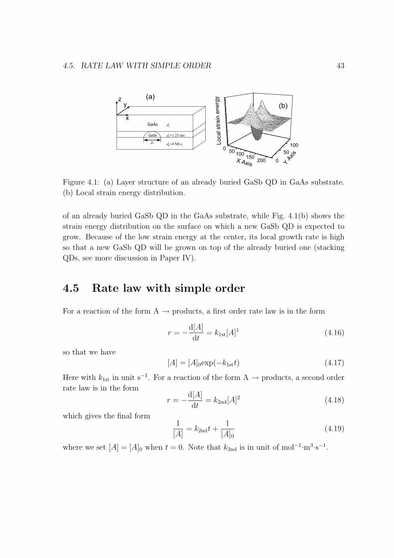
4.5. RATE LAW WITH SIMPLE ORDER 43
050100
150200 0
50
100
GaSb
D
d1=1.25 nm
d0=4 MLs
d2
GaAs
x
yz
Local strain energy
Y Axis
X Axis
(b)
(a)
Figure 4.1: (a) Layer structure of an already buried GaSb QD in GaAs substrate.
(b) Local strain energy distribution.
of an already buried GaSb QD in the GaAs substrate, while Fig. 4.1(b) shows the
strain energy distribution on the surface on which a new GaSb QD is expected to
grow. Because of the low strain energy at the center, its local growth rate is high
so that a new GaSb QD will be grown on top of the already buried one (stacking
QDs, see more discussion in Paper IV).
4.5 Rate law with simple order
For a reaction of the form A → products, a first order rate law is in the form
r = −d[A]
dt= k1st[A]1 (4.16)
so that we have
[A] = [A]0exp(−k1stt) (4.17)
Here with k1st in unit s−1. For a reaction of the form A → products, a second order
rate law is in the form
r = −d[A]
dt= k2nd[A]2 (4.18)
which gives the final form1
[A]= k2ndt +
1
[A]0(4.19)
where we set [A] = [A]0 when t = 0. Note that k2nd is in unit of mol−1·m3·s−1.

44 CHAPTER 4. CHEMICAL KINETICS
Chapter 5
Computational fluid dynamics
method
The mathematical models presented here is to describe the complex interaction
between the gas-phase fluid dynamics and the heat and individual species transport
in MOCVD. The models consist of a set of partial differential equations (PDEs)
with appropriate boundary conditions, describing the fluid flow, the transport of
energy and species and the chemical reactions in the reactor. Several transport
properties of gas species and mixtures enter in these equations. Their values depend
on the temperature, pressure and composition of the gas mixture. The chemical
reactions in the gas-phase and at the substrate surface are described in a general
way that is applicable to many different semiconductor materials. Knowledge of the
specific chemical mechanisms and kinetics is necessary for the actual modeling of a
particular compound system.
Numerical methods are required to solve the nonlinear set of governing equations.
The equations are solved via the finite element method (FEM), which is a natu-
rally suited approach to solving the coupled, nonlinear PDEs arising in fluid flow,
heat and mass transfer calculations. In the FEM procedure, a mesh is generated by
computational domain into many regularly shaped elements. Piecewise polynomials
represent the solution. By applying a Galerkin approximation, the PDEs governing
transport phenomena and reaction are converted in a set of coupled algebraic equa-
tions in the unknown node values of the polynomial approximation. The resulting
system of equations is then solved by using Newton’s method.
45
46 CHAPTER 5. COMPUTATIONAL FLUID DYNAMICS METHOD
5.1 Fundamental assumptions
First of all, we need to make some assumptions in order to simplify the physics of
the process and reduce the computation time to tractable levels. These assumptions
are generally justified for typical CVD conditions and essentially do not limit the
accuracy and pertinence of the model for CVD applications.
• Assumption: the gas mixture behaves as s continuum. This approach is ap-
propriate because the Knudsen number, the ratio of the mean free path to the
length scale over which macroscopic changes in properties occur, is smaller
than 0.1 when operating under reduced or atmospheric pressures character-
istic of most MOCVD systems. As a point of reference, the mean free path
length at 76 torr and 400C is approximately 2.6 and 1.6 µm in H2 and N2
carrier gas, respectively.
• Assumption: the gases follow the ideal gas law. This is valid for the types of
gases and at the low pressure and high temperature used in CVD. The ideal
gas law provides the gas density dependence on temperature, that is needed
to capture gas expansion effects due to density changes caused by the large
temperature differences (about 600 ∼ 1000 K) between the hot substrate and
the cold walls.
• Assumption: the gas flow in the reactor is laminar. This is valid for the
Reynolds number range typically encountered in CVD. The Reynolds number
is a dimensionless number that gives a measure of the ratio of inertial forces
to viscous forces. Consequently, it quantifies the relative importance of these
two types of forces for given flow conditions. Typically, it takes values in the
range between 1 and 100. This range is much lower than the values at the
onset of turbulence in a reactor (approximately 2300 for pipe flow, and 1000
for free jet flow).
• Assumption: the gas density depends only on temperature. The very low
Mach numbers, i.e., the ratio of the gas velocity in the reactor to the speed of
sound, encountered in CVD justify this assumption.
• Furthermore, since the pressure drop in the CVD reactor is very small (' 10−6
atm), the pressure imposed at the reactor outlet is assumed to be a constant
and is used in the ideal gas law to calculate the density.
5.2. NAVIER-STOKES EQUATIONS 47
• A steady-state formulation is used. This assumption is valid because the time
scale for deposition of thin semiconductor films (growth rate ∼ 1µm/hr) is
much longer than the time scale for convective and diffusive transport processes
in the gas which is on the order of seconds. Thus, transient terms can be safely
dropped from the modeling equations of steady-state deposition processes.
• Similarly, the thin film length scale on the order of microns is much smaller
than the characteristic length scale of gas flow in the reactor, and the time
evolution of the film profile can be neglected.
• The fluid flow and heat transfer are decoupled from the mass transfer.
• The reactant species and the reaction products are present in low concentra-
tions in the orders of 10−5 mole fraction in a carrier gas, typically H2 or N2.
Thus the properties of the gas mixture present in the reactor remain constant
and equal to those of the carrier gas. Even in the case of III-nitride deposition
(where comparable amounts of H2 or N2 and NH3 are used) the organometallic
precursors and the reaction products are still present in trace amounts. Since
negligible homogeneous NH3 decomposition occurs, the carrier gas can be as-
sumed to be a constant-composition mixture of H2(N2) and NH3. Mixing rules
are used to compute the “effective” carrier gas transport properties (viscosity,
thermal conductivity, heat capacity) that are used in the fluid flow and heat
transfer calculations.
• Since the mass loss due to deposition is negligible, no source/drain terms are
present in the total mass conservation equation and it may then be decoupled
from the chemistry.
• The energy conservation equation can also be decoupled from the chemistry
since heat consumption or dissipation by gas-phase reactions can be neglected
due to the dilute nature of the reactants.
5.2 Navier-Stokes equations
In the numerical computational CFD, there are two basic laws,
• The conservation of fluid mass
• The change of momentum equals to the total impulse to the body.
48 CHAPTER 5. COMPUTATIONAL FLUID DYNAMICS METHOD
The two laws result in Navier-Stokes (NS) equations. Conservation of mass (mass
continuity equation) requires that the time rate of change of mass in a control volume
be balanced by the net mass flow into the same control volume,
∂ρ
∂t+∇ · (ρ~V ) =
∂ρ
∂t+
∂(ρu)
∂x+
∂(ρv)
∂y+
∂(ρw)
∂z= 0 (5.1)
where ~V is the flow velocity, ρ is the fluid density, u, v and w are the velocity com-
ponents of x, y and z respectively. Conservation of momentum: The x-component
of the momentum equation is found by setting the rate of change of x-momentum
of the fluid particle equal to the total force in the x-direction on the element due to
surface stresses plus the rate of increase of x-momentum due to sources:
∂(ρu)
∂t+∇ · (ρ~V u) =
∂(−p + τxx)
∂x+
∂τyx
∂y+
∂τzx
∂z+ SMx (5.2)
Similar equations can be written for the y- and z-components of the momentum
equation:
∂(ρv)
∂t+∇ · (ρ~V v) =
∂τxy
∂x+
∂(−p + τyy)
∂y+
∂τzy
∂z+ SMy
∂(ρw)
∂t+∇ · (ρ~V w) =
∂τxz
∂x+
∂τyz
∂y+
∂(−p + τzz)
∂z+ SMz (5.3)
In these equations p is the static pressure, τij (i, j = x, y, z) is the viscous stress
tensor and SMx , SMy , SMz are source terms.
The above momentum equations contain as unknowns the viscous stress components
τij. A model must be provided to define the viscous stresses. In Newtonian flows
the viscous stresses are proportional to the deformation rates. The nine viscous
stress components (of which six are independent for isotropic fluids) can be related
to velocity gradients to produce the following shear stress terms:
τxx = 2µ∂u
∂x− 2
3µ(∇ · ~V ) , τyy = 2µ
∂v
∂y− 2
3µ(∇ · ~V )
τzz = 2µ∂w
∂z− 2
3µ(∇ · ~V ) , τxy = τyx = µ
(∂u
∂y+
∂v
∂x
)
τxz = τzx = µ
(∂u
∂z+
∂w
∂x
), τyz = τzy = µ
(∂v
∂z+
∂w
∂y
)(5.4)
Substitution of the above shear stress terms into the momentum equations yields
the NS equations:
5.3. BRIEF INTRODUCTION OF CFD-ACE+ 49
∂(ρu)
∂t+∇ · (ρ~V u) = −∂p
∂x+∇ · (µ∇u) + SMx
∂(ρv)
∂t+∇ · (ρ~V v) = −∂p
∂y+∇ · (µ∇v) + SMy
∂(ρw)
∂t+∇ · (ρ~V w) = −∂p
∂z+∇ · (µ∇w) + SMz (5.5)
5.3 Brief introduction of CFD-ACE+
CFD-ACE+ is a set of computer programs for multi-physics computational anal-
ysis. The programs provide an integrated geometry and grid generation module,
a graphical user interface for preparing the model, a computational solver for per-
forming the simulation, and an interactive visualization program for examining and
analyzing the simulation results. The standard CFD-ACE+ package includes the
following applications: [82]
CFD-GEOM geometry and grid generation, which provides geometric modeling
and structured and unstructured grid generation capability.
CFD-ACE-GUI graphical user interface
CFD-ACE-Solver advanced polyhedral solver
CFD-VIEW post processor, which provides visualization and analysis tools for
examining calculated results
Incompressible/Compressible
Steady/Unsteady
Turbulent Model
Laminar Flow, with a choice of non-Newtonian Rheology
Stationary and rotating frames of reference
Volume of Fluid (VOF) free surface modeling with surface tension
Porous media
Heat transfer including solid conduction
Surface-to-surface radiation
Chemical reaction models
Multi-component fluids
Coupling computing (structural, Electro-Physic ...)
MEMS
50 CHAPTER 5. COMPUTATIONAL FLUID DYNAMICS METHOD
5.4 Application: Thin film growth
We adopt Sengupta’s model [65] for the gas-phase reactions where the CFD method
of Ref. [75] is used to obtain detailed information about spatial distributions of
concentrations of radicals in the reactor where the abundant Ga species (MMG
and MMG:NH3) on the film surface are assumed to be the principal radicals for the
surface growth. The geometry of a vertical reactor is schematically shown in Fig. 5.1
[67]. Inflow gas contains TMG, NH3 and H2, and the total flux is kept constant at
14 slm (L/min). The flux of TMG at the inlet is also kept constant at 30 sccm
(mL/min) at 300 K. NH3/TMG (V/III) ratio will thus be modified when the flux of
NH3 is changed. The temperature of the susceptor, Ts, varies between 700 and 1500
K, since TMG begins pyrolyzing at 475 C and GaN begins to dissociate when the
substrate temperature exceeds 1100 C [77]. The V/III ratio is kept constant to be
2000 in this work, as commonly reported in literatures [83, 84, 85, 86]. Moreover,
low-pressure MOCVD (P ∼ 100 Torr) is normally adopted to grow GaN films [77].
The reactor pressure P in this work has also been kept constant (=100 Torr). Note
that rate constants are pressure dependent [65]. In the reactor system of Thomas
Swan, the relationship between volume flux f (in unit of sccm) and mole flux µ (in
unit of mol/min) in the inlet gas is given by
µ = αf (5.6)
for TMG, α = 2.773 × 10⁻⁶; for NH3 and H2, α = 4.051 × 10⁻⁵, which we have
adopted in our numerical simulations.
For a standard reactor of Fig. 5.1 which specifies the reactor’s geometry and bound-
ary conditions, the nominal growth conditions are Ts = 1373 K, P = 100 Torr, and
V/III=2000. The stream function, temperature, and spatial distribution of radi-
cals in such a reactor, i.e., in the shadow area in Fig. 5.1(b), are shown in Fig. 5.2
obtained from the CFD simulation. Figure 5.2(b) shows that the temperature in
the middle of the reactor is the highest due to the exothermic reaction occurred in
the gas phase. When the susceptor is heated uniformly as assumed in the model,
dT/dx ≈ 0.0 in the vicinity of the upper surface of the wafer. Such a small tem-
perature gradient is important for the uniformity of the film growth. The main Ga
species, i.e., MMG and MMG:NH3 in Figs. 5.2(c)(d), are generated in the middle of
the reactor in the gas phase. They are largely depleted on the wafer surface. Their
concentration gradients along the horizon directions are also small for uniform film
growth. Meanwhile, the by-product of surface reaction, CH4 in Fig. 5.2(e), appears
on the wafer surface.
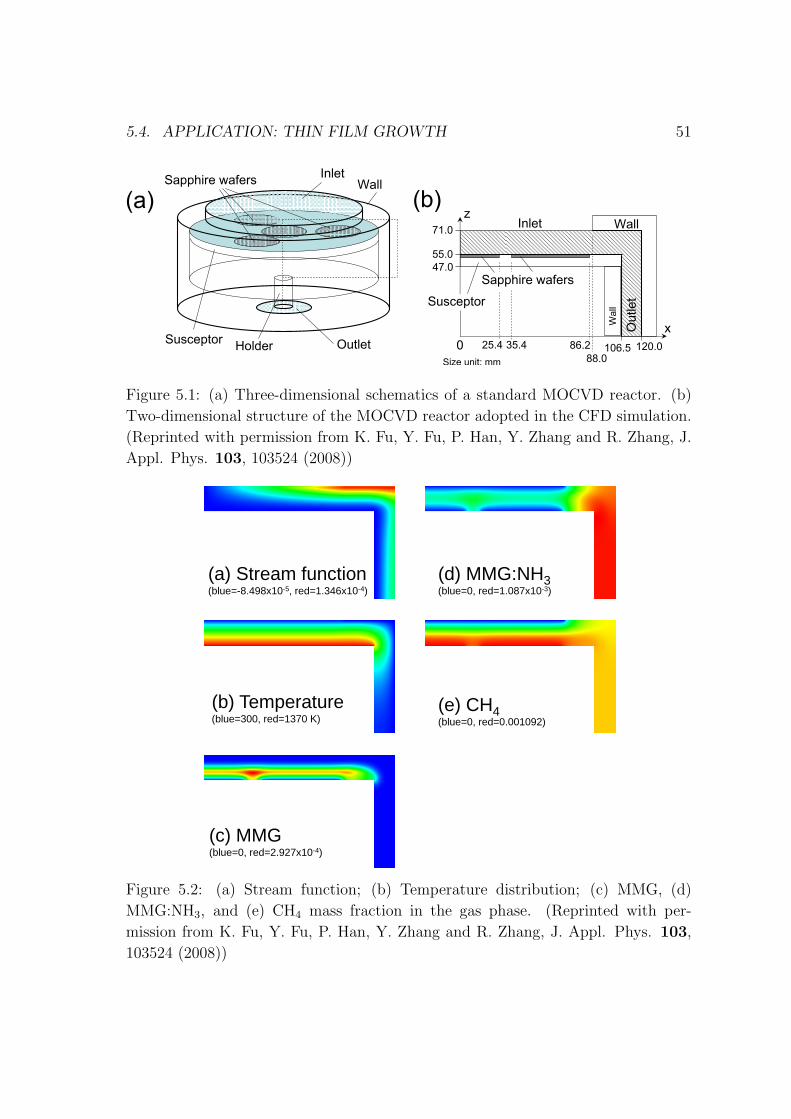
5.4. APPLICATION: THIN FILM GROWTH 51
Inlet
Outlet
Wall
Susceptor
Sapphire wafers
Holder
(a)
Sapphire wafers
WallInlet
106.5 120.088.0
86.2
z
Susceptor
71.0
55.0
x
35.425.40
Outlet
47.0
(b)
Size unit: mm
Wall
Figure 5.1: (a) Three-dimensional schematics of a standard MOCVD reactor. (b)
Two-dimensional structure of the MOCVD reactor adopted in the CFD simulation.
(Reprinted with permission from K. Fu, Y. Fu, P. Han, Y. Zhang and R. Zhang, J.
Appl. Phys. 103, 103524 (2008))
(e) CH4(blue=0, red=0.001092)
(c) MMG(blue=0, red=2.927x10⁻⁴)
(d) MMG:NH3(blue=0, red=1.087x10⁻³)
(a) Stream function(blue=-8.498x10⁻⁵, red=1.346x10⁻⁴)
(b) Temperature(blue=300, red=1370 K)
Figure 5.2: (a) Stream function; (b) Temperature distribution; (c) MMG, (d)
MMG:NH3, and (e) CH4 mass fraction in the gas phase. (Reprinted with per-
mission from K. Fu, Y. Fu, P. Han, Y. Zhang and R. Zhang, J. Appl. Phys. 103,
103524 (2008))
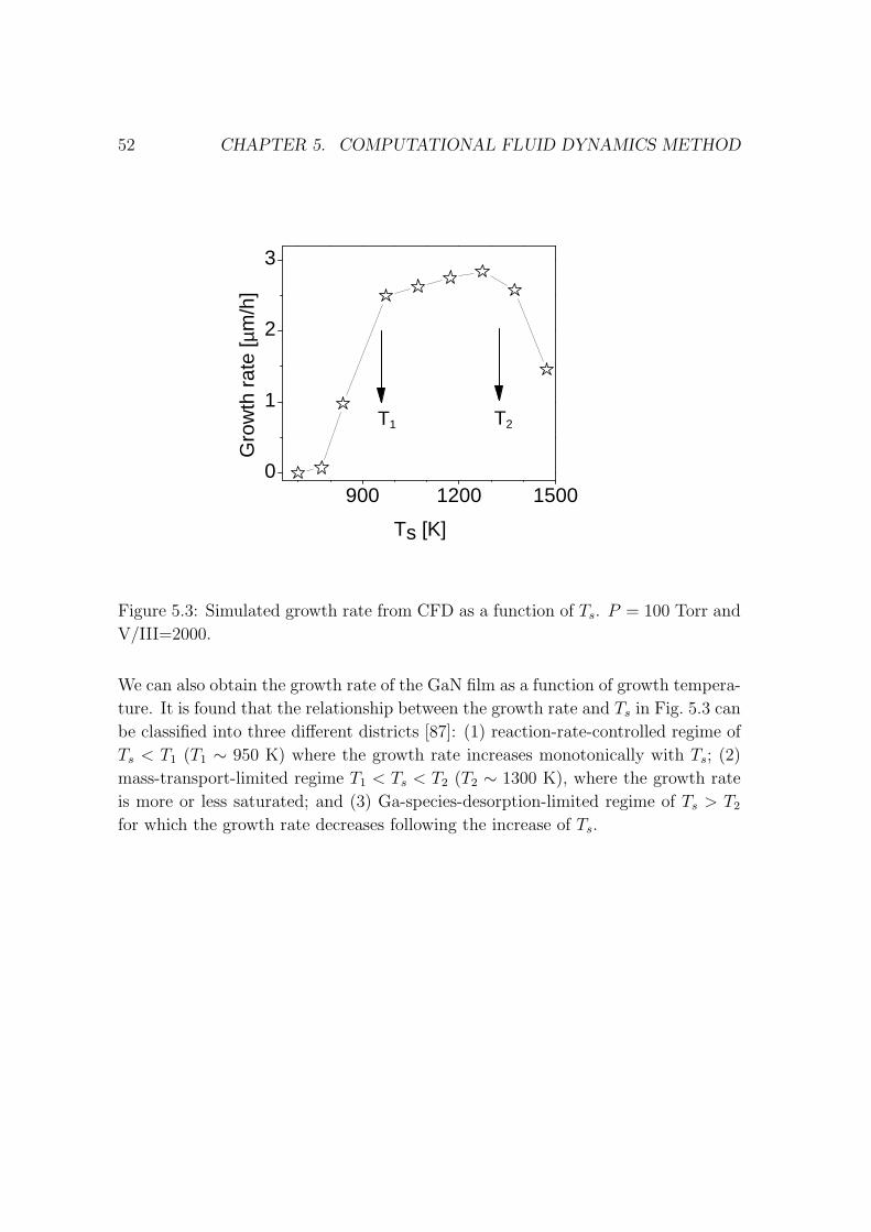
52 CHAPTER 5. COMPUTATIONAL FLUID DYNAMICS METHOD
900 1200 15000
1
2
3
T1
Ts [K]
Gro
wth
rat
e [µ
m/h
]
T2
Figure 5.3: Simulated growth rate from CFD as a function of Ts. P = 100 Torr and
V/III=2000.
We can also obtain the growth rate of the GaN film as a function of growth tempera-
ture. It is found that the relationship between the growth rate and Ts in Fig. 5.3 can
be classified into three different districts [87]: (1) reaction-rate-controlled regime of
Ts < T1 (T1 ∼ 950 K) where the growth rate increases monotonically with Ts; (2)
mass-transport-limited regime T1 < Ts < T2 (T2 ∼ 1300 K), where the growth rate
is more or less saturated; and (3) Ga-species-desorption-limited regime of Ts > T2
for which the growth rate decreases following the increase of Ts.
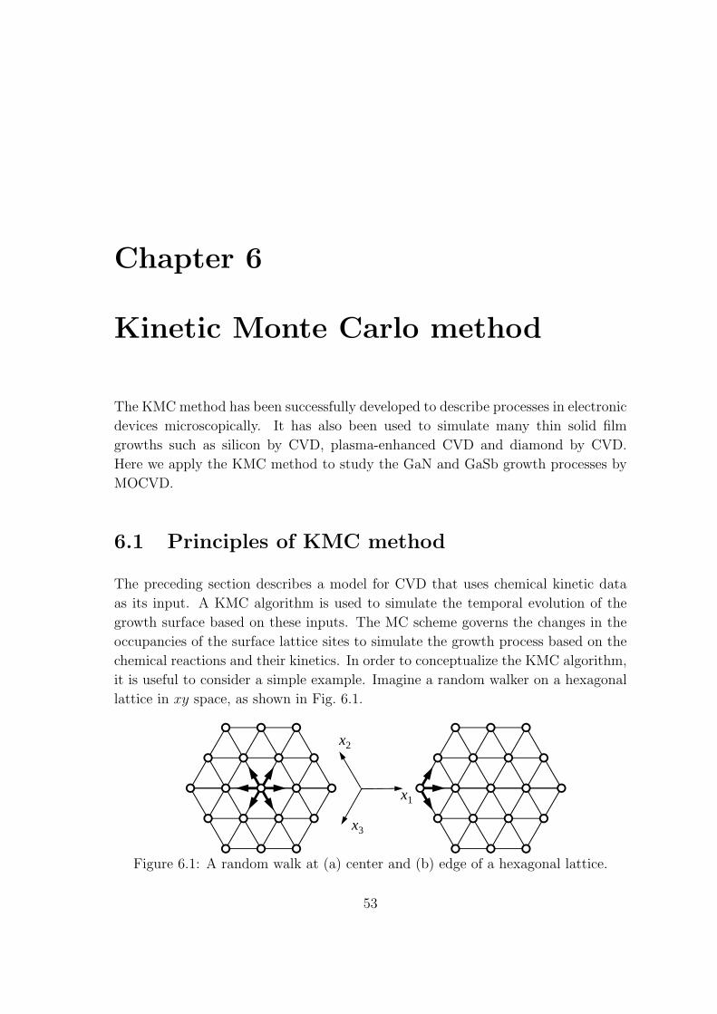
Chapter 6
Kinetic Monte Carlo method
The KMC method has been successfully developed to describe processes in electronic
devices microscopically. It has also been used to simulate many thin solid film
growths such as silicon by CVD, plasma-enhanced CVD and diamond by CVD.
Here we apply the KMC method to study the GaN and GaSb growth processes by
MOCVD.
6.1 Principles of KMC method
The preceding section describes a model for CVD that uses chemical kinetic data
as its input. A KMC algorithm is used to simulate the temporal evolution of the
growth surface based on these inputs. The MC scheme governs the changes in the
occupancies of the surface lattice sites to simulate the growth process based on the
chemical reactions and their kinetics. In order to conceptualize the KMC algorithm,
it is useful to consider a simple example. Imagine a random walker on a hexagonal
lattice in xy space, as shown in Fig. 6.1.
x1
x3
x2
Figure 6.1: A random walk at (a) center and (b) edge of a hexagonal lattice.
53
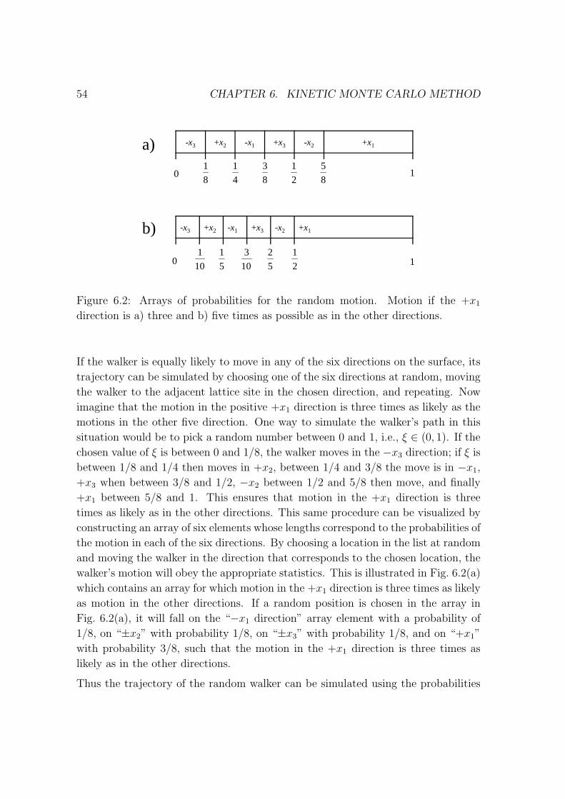
54 CHAPTER 6. KINETIC MONTE CARLO METHOD
4
1
-x3 +x2 -x1 +x3 -x2 +x1
0 18
3
2
1
8
5
8
1
-x3 +x2 -x1 +x3 -x2 +x1
a)
b)
10
1
5
10 110
3
5
2
2
1
Figure 6.2: Arrays of probabilities for the random motion. Motion if the +x1
direction is a) three and b) five times as possible as in the other directions.
If the walker is equally likely to move in any of the six directions on the surface, its
trajectory can be simulated by choosing one of the six directions at random, moving
the walker to the adjacent lattice site in the chosen direction, and repeating. Now
imagine that the motion in the positive +x1 direction is three times as likely as the
motions in the other five direction. One way to simulate the walker’s path in this
situation would be to pick a random number between 0 and 1, i.e., ξ ∈ (0, 1). If the
chosen value of ξ is between 0 and 1/8, the walker moves in the −x3 direction; if ξ is
between 1/8 and 1/4 then moves in +x2, between 1/4 and 3/8 the move is in −x1,
+x3 when between 3/8 and 1/2, −x2 between 1/2 and 5/8 then move, and finally
+x1 between 5/8 and 1. This ensures that motion in the +x1 direction is three
times as likely as in the other directions. This same procedure can be visualized by
constructing an array of six elements whose lengths correspond to the probabilities of
the motion in each of the six directions. By choosing a location in the list at random
and moving the walker in the direction that corresponds to the chosen location, the
walker’s motion will obey the appropriate statistics. This is illustrated in Fig. 6.2(a)
which contains an array for which motion in the +x1 direction is three times as likely
as motion in the other directions. If a random position is chosen in the array in
Fig. 6.2(a), it will fall on the “−x1 direction” array element with a probability of
1/8, on “±x2” with probability 1/8, on “±x3” with probability 1/8, and on “+x1”
with probability 3/8, such that the motion in the +x1 direction is three times as
likely as in the other directions.
Thus the trajectory of the random walker can be simulated using the probabilities
6.1. PRINCIPLES OF KMC METHOD 55
of the motion in each direction along with a simple MC algorithm. This algorithm
can easily be generalized to obtain the trajectory (spatial, temporal, configurational,
etc.) of a system using the probabilities of the events that can potentially occur at
each location, time or configuration. In the case of the random walker, the same
six events can occur at each lattice site, though the probabilities need not be the
same at each site. The set of possible events could also change depending on the
configuration. For example, the random walker might be allowed to move in one of
only three directions (at the edges of the hexagonal lattice as in Fig. 6.1(b), or there
might be special lattice sites for which motion in the +x1 (or some other) direction
is five times as likely as in the other directions. These possibilities can be handled
simply by allowing different selection criteria at each lattice site. Whenever the
walker landed on a lattice site for which the motion in the +x1 direction was three
times as likely as in the other direction, then an array like the one in Fig. 6.2(a)
would be used to choose the walker’s next move. When the walker landed on a
lattice site for which motion in the +x1 direction was five times as likely as in the
other directions, the array in Fig. 6.2(b) could be used. The number and relative
sizes of the array elements can be modified to account for virtually arbitrary changes
in the sets of possible evolutionary pathways at different configurations.
This approach can be applied to any problem wherein a discrete system (e.g., a
random walker on a lattice or the atoms on the surface of a growing film) evolves
according to a finite set of events (e.g., walks or reactions) whose probabilities are
known. Given the initial state of a system and the set of events by which the system
can evolve, the evolution of the system can be simulated. Consider a system in a
particular configuration such that M events, labeled i = 1, 2, 3, ..., M , can occur with
probabilities p1, p2, p3, ..., pM . The evolution of the system is simulated by picking
one of the M events at random, such that the probability of choosing even i is pi,
and then applying the corresponding change to the system’s configuration. This
event, denoted m, is selected by choosing a random number, ξ1 ∈ (0, 1), and picking
the event whose occurrence probability obeys the following equation:m−1∑i=0
pi ≤ ξ1 <
m∑i=0
pi (6.1)
where p0 = 0. This is the same procedure that was used to choose the direction
for the random walker, for which there were only six possible events (M = 6). In
the case where motion in the +x1 direction was three times as likely as motion in
the other directions, p1 = p2 = p3 = p4 = p5 = 1/8 and p6 = 3/8 where events
i = 1, 2, ..., 5 are motions in the −x1, ±x2, and ±x3 directions, respectively, and
i = 6 is motion in the +x1 direction.
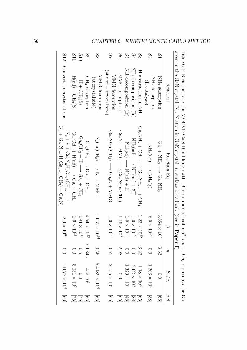
56 CHAPTER 6. KINETIC MONTE CARLO METHOD
Tab
le6.1:
Reaction
ratesfor
MO
CV
DG
aNth
in-fi
lmgrow
th.
Ais
inunits
ofm
ol,cm
3,an
ds.
Ga
crep
resents
the
Ga
atomin
the
GaN
crystal,
Nc :
Natom
inG
aNcry
stal,∗:su
rfacebi-rad
ical.(S
eein
Paper
I)
Reaction
Reaction
Eq.
An
Ea /R
Ref.
S1
NH
3ad
sorption
Ga
c+
NH
3 −→G
ac N
H3
3.354×10
73.33
0.0[65]
S2
NH
3desorp
tion
(Ircataly
ze)N
H3 (ad
)−→N
H3 (g)
6.0×10
14
0.01.203×
104
[88]
S3
Hab
stractionin
NH
xG
ac N
Hx+
CH
3 −→G
ac N
Hx−
1+
CH
41.23×
1010
3.221.18×
104
[65]
S4
NH
3decom
position
(Ir)N
H3 (ad
)−→N
H(ad
)+
2H1.0×
1012
0.09.62×
103
[88]
S5
NH
decom
position
(Ir)N
H(ad
)−→N
(ad)+
H1.0×
1011
0.01.323×
104
[88]
S6
MM
Gad
sorption
Ga
c N+
MM
G−→
Ga
c NG
a(CH
3 )1.16×
105
2.980.0
[65]
S7
MM
Gdesorp
tion
(atnon−
crystalsite)
Ga
c NG
a(CH
3 )−→G
ac N
+M
MG
1.0×10
14
0.552.155×
104
[65]
S8
MM
Gdesorp
tion
(atcry
stalsite)N
c Ga(C
H3 )−→
Nc+
MM
G1.115×
1014
0.555.4189×
104
[65]
S9
CH
3desorp
tionG
ac C
H3 −→
Ga
c+
CH
34.54×
1013
0.03464×
104
[65]
S10
H+
CH
3 (S)
Ga
c CH
3+
H−→
Ga
c+
CH
44.94×
1011
0.50.0
[75]
S11
H(ad
)+
CH
3 (S)
Ga
c CH
3+
H(ad
)−→G
ac+
CH
41.0×
1016
0.05.051×
103
[75]
S12
Con
vertto
crystal
atoms
Nc+∗
+G
ac N
x Hz G
ay (C
H3 )−→
Nc+
Ga
c Nx−
1 Hz G
ay−
1 (CH
3 )+
Ga
c Nc
2.0×10
80.0
1.1072×10
4[66]
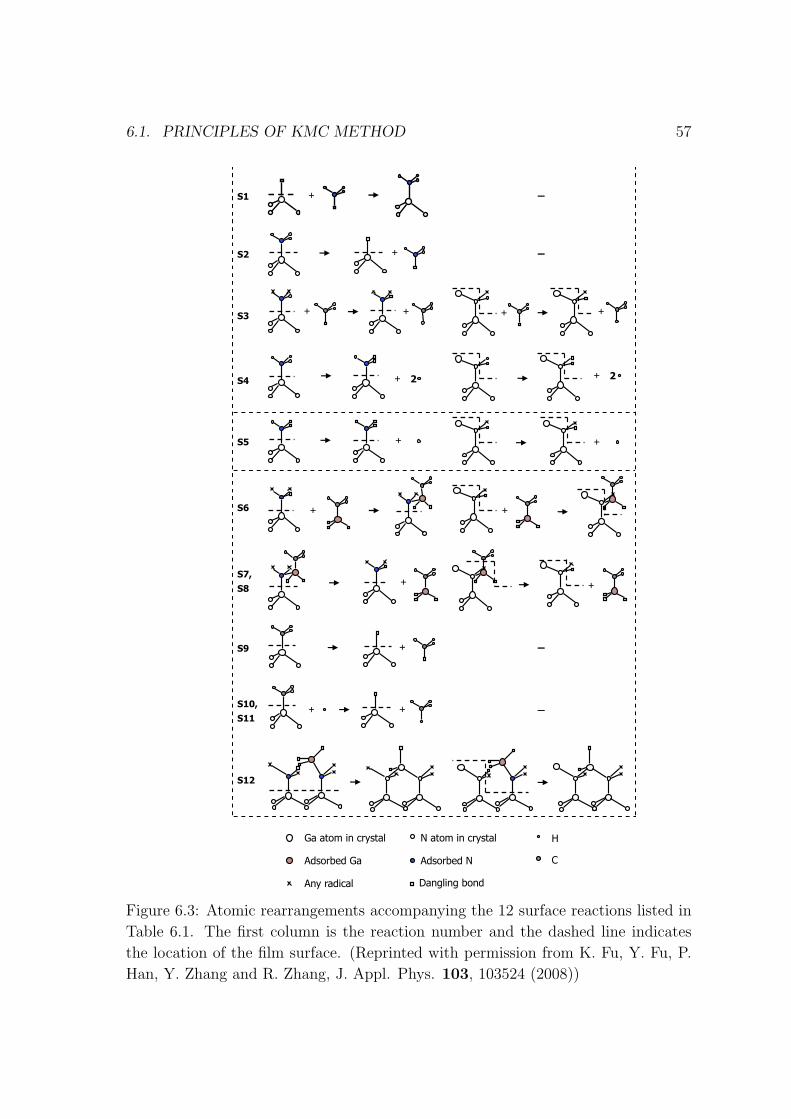
6.1. PRINCIPLES OF KMC METHOD 57
S1
――――
S2
――――
S3
S4
S5
S6
S7,
S8
S9
――――
S10,
S11
――――
S12
Ga atom in crystal N atom in crystal H
Adsorbed Ga Adsorbed N C
Any radical Dangling bond
+ +
+
+ +
+ +
+ +
+ 2 + 2
+ + + +
+ D
+
Figure 6.3: Atomic rearrangements accompanying the 12 surface reactions listed in
Table 6.1. The first column is the reaction number and the dashed line indicates
the location of the film surface. (Reprinted with permission from K. Fu, Y. Fu, P.
Han, Y. Zhang and R. Zhang, J. Appl. Phys. 103, 103524 (2008))
58 CHAPTER 6. KINETIC MONTE CARLO METHOD
This same scheme can be used to describe the growth surface in a lattice based CVD
simulation. Here I first begin with the expression of surface reactions during GaN
film growth at microscopic level. All kinds of the reactions that could occur over the
surface in GaN MOCVD grwoth are provided in Table 6.1, including the adsorpation
and desorption of radicals and crystallization of atoms. A schematic representation
of atomic re-arrangements accompanying all relevant surface reactions is shown in
Fig. 6.3. The dashed lines indicate the location of the surface. The atomic rear-
rangements accompanying the reactions in the second column of Fig. 6.3 pertain to
the cases when that reactions take place on surface terraces, while at surface steps
in the third column. Given a set of reactions like the one in Table 6.1, all of the
chemical reactions that can occur at all sites on a surface in a given configuration
can be identified. Furthermore, the rate of each individual reaction can be deter-
mined (from Chapter 4). The probability of one particular reaction occurring at one
particular site is simply its rate divided by the sum of the rates of all the reactions
that are possible at all surface sites. Thus, given the M events (i.e., individual re-
actions at individual surface sites) that can occur on a surface, and their rates, the
evolution of the surface can be simulated by choosing one of the events, m, based
on a random number ξ1 ∈ (0, 1), according to
m−1∑i=0
ri
M∑i=0
ri
≤ ξ1 <
m∑i=0
ri
M∑i=0
ri
(6.2)
where ri is the rate (per-site in units of sec−1) of the reaction corresponding to
event i, and r0 = 0. This selection criterion ensures that one reaction occurs at
each simulation step, and that fast events (i.e., those with large rates) are more
likely to be chosen than slow events. Once event m is chosen and executed, the
procedure is repeated for the modified system using a new set of possible events
which correspond to the updated system configuration. Since the set of events are
possibly different as a function of the evolution time, the time increment, dt, is thus
not uniform throughout the simulation. It must account for the “reactivity” of the
surface at each simulation time step,
dt = − ln(ξ2)M∑i=0
ri
(6.3)
where ξ2 is a random number such that ξ2 ∈ (0, 1). When fast events are occurring
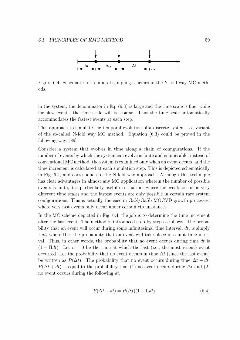
6.1. PRINCIPLES OF KMC METHOD 59
t…∆t1 ∆t2 ∆t3
Figure 6.4: Schematics of temporal sampling schemes in the N-fold way MC meth-
ods.
in the system, the denominator in Eq. (6.3) is large and the time scale is fine, while
for slow events, the time scale will be coarse. Thus the time scale automatically
accommodates the fastest events at each step.
This approach to simulate the temporal evolution of a discrete system is a variant
of the so-called N-fold way MC method. Equation (6.3) could be proved in the
following way. [89]
Consider a system that evolves in time along a chain of configurations. If the
number of events by which the system can evolve is finite and enumerable, instead of
conventional MC method, the system is examined only when an event occurs, and the
time increment is calculated at each simulation step. This is depicted schematically
in Fig. 6.4, and corresponds to the N-fold way approach. Although this technique
has clear advantages in almost any MC application wherein the number of possible
events is finite, it is particularly useful in situations where the events occur on very
different time scales and the fastest events are only possible in certain rare system
configurations. This is actually the case in GaN/GaSb MOCVD growth processes,
where very fast events only occur under certain circumstances.
In the MC scheme depicted in Fig. 6.4, the job is to determine the time increment
after the last event. The method is introduced step by step as follows. The proba-
bility that an event will occur during some infinitesimal time interval, dt, is simply
Πdt, where Π is the probability that an event will take place in a unit time inter-
val. Thus, in other words, the probability that no event occurs during time dt is
(1 − Πdt). Let t = 0 be the time at which the last (i.e., the most recent) event
occurred. Let the probability that no event occurs in time ∆t (since the last event)
be written as P (∆t). The probability that no event occurs during time ∆t + dt,
P (∆t + dt) is equal to the probability that (1) no event occurs during ∆t and (2)
no event occurs during the following dt,
P (∆t + dt) = P (∆t)(1− Πdt) (6.4)
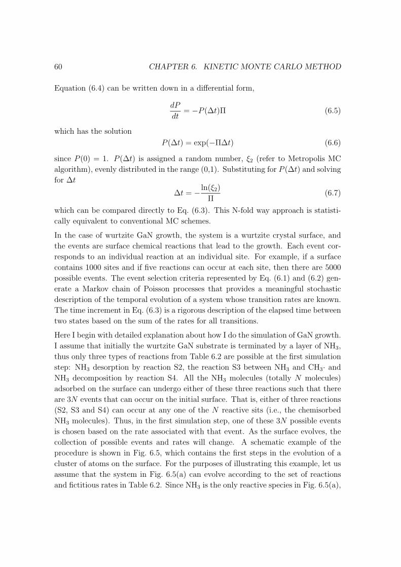
60 CHAPTER 6. KINETIC MONTE CARLO METHOD
Equation (6.4) can be written down in a differential form,
dP
dt= −P (∆t)Π (6.5)
which has the solution
P (∆t) = exp(−Π∆t) (6.6)
since P (0) = 1. P (∆t) is assigned a random number, ξ2 (refer to Metropolis MC
algorithm), evenly distributed in the range (0,1). Substituting for P (∆t) and solving
for ∆t
∆t = − ln(ξ2)
Π(6.7)
which can be compared directly to Eq. (6.3). This N-fold way approach is statisti-
cally equivalent to conventional MC schemes.
In the case of wurtzite GaN growth, the system is a wurtzite crystal surface, and
the events are surface chemical reactions that lead to the growth. Each event cor-
responds to an individual reaction at an individual site. For example, if a surface
contains 1000 sites and if five reactions can occur at each site, then there are 5000
possible events. The event selection criteria represented by Eq. (6.1) and (6.2) gen-
erate a Markov chain of Poisson processes that provides a meaningful stochastic
description of the temporal evolution of a system whose transition rates are known.
The time increment in Eq. (6.3) is a rigorous description of the elapsed time between
two states based on the sum of the rates for all transitions.
Here I begin with detailed explanation about how I do the simulation of GaN growth.
I assume that initially the wurtzite GaN substrate is terminated by a layer of NH3,
thus only three types of reactions from Table 6.2 are possible at the first simulation
step: NH3 desorption by reaction S2, the reaction S3 between NH3 and CH3· and
NH3 decomposition by reaction S4. All the NH3 molecules (totally N molecules)
adsorbed on the surface can undergo either of these three reactions such that there
are 3N events that can occur on the initial surface. That is, either of three reactions
(S2, S3 and S4) can occur at any one of the N reactive sits (i.e., the chemisorbed
NH3 molecules). Thus, in the first simulation step, one of these 3N possible events
is chosen based on the rate associated with that event. As the surface evolves, the
collection of possible events and rates will change. A schematic example of the
procedure is shown in Fig. 6.5, which contains the first steps in the evolution of a
cluster of atoms on the surface. For the purposes of illustrating this example, let us
assume that the system in Fig. 6.5(a) can evolve according to the set of reactions
and fictitious rates in Table 6.2. Since NH3 is the only reactive species in Fig. 6.5(a),
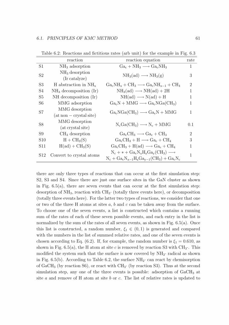
6.1. PRINCIPLES OF KMC METHOD 61
Table 6.2: Reactions and fictitious rates (arb unit) for the example in Fig. 6.3
reaction reaction equation rate
S1 NH3 adsorption Gac + NH3 −→ GacNH3 1
S2NH3 desorption
(Ir catalyze)NH3(ad) −→ NH3(g) 3
S3 H abstraction in NHx GacNHx + CH3 −→ GacNHx−1 + CH4 2
S4 NH3 decomposition (Ir) NH3(ad) −→ NH(ad) + 2H 1
S5 NH decomposition (Ir) NH(ad) −→ N(ad) + H 1
S6 MMG adsorption GacN + MMG −→ GacNGa(CH3) 1
S7MMG desorption
(at non− crystal site)GacNGa(CH3) −→ GacN + MMG 1
S8MMG desorption
(at crystal site)NcGa(CH3) −→ Nc + MMG 0.1
S9 CH3 desorption GacCH3 −→ Gac + CH3 2
S10 H + CH3(S) GacCH3 + H −→ Gac + CH4 3
S11 H(ad) + CH3(S) GacCH3 + H(ad) −→ Gac + CH4 1
S12 Convert to crystal atomsNc + ∗+ GacNxHzGay(CH3) −→
Nc + GacNx−1HzGay−1(CH3) + GacNc1
there are only three types of reactions that can occur at the first simulation step:
S2, S3 and S4. Since there are just one surface sites in the GaN cluster as shown
in Fig. 6.5(a), there are seven events that can occur at the first simulation step:
desorption of NH3, reaction with CH3· (totally three events here), or decomposition
(totally three events here). For the latter two types of reactions, we consider that one
or two of the three H atoms at sites a, b and c can be taken away from the surface.
To choose one of the seven events, a list is constructed which contains a running
sum of the rates of each of these seven possible events, and each entry in the list is
normalized by the sum of the rates of all seven events, as shown in Fig. 6.5(a). Once
this list is constructed, a random number, ξ1 ∈ (0, 1) is generated and compared
with the numbers in the list of summed relative rates, and one of the seven events is
chosen according to Eq. (6.2). If, for example, the random number is ξ1 = 0.610, as
shown in Fig. 6.5(a), the H atom at site c is removed by reaction S3 with CH3·. This
modified the system such that the surface is now covered by NH2· radical as shown
in Fig. 6.5(b). According to Table 6.2, the surface NH2· can react by chemisorption
of GaCH3 (by reaction S6), or react with CH3· (by reaction S3). Thus at the second
simulation step, any one of the three events is possible: adsorption of GaCH3 at
site a and remove of H atom at site b or c. The list of relative rates is updated to
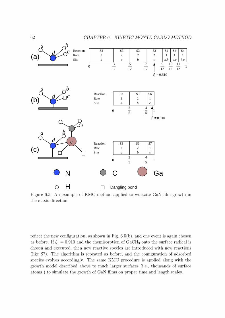
62 CHAPTER 6. KINETIC MONTE CARLO METHOD
Reaction S2 S3 S3 S3 S4 S4 S4Rate 3 2 2 2 1 1 1Site d a b c a,b a,c b,c
Reaction S3 S3 S6Rate 2 2 1Site a b c
a bcd
cda b
bcd
a
(a)
(b)
012
3
12
5
12
7
12
9
12
10
12
111
610.01 =ξ
05
2
5
41
910.01 =ξ
Reaction S3 S3 S7Rate 2 2 1Site a b c
cd
(c)
N C Ga
H Dangling bond
05
2
5
41
Figure 6.5: An example of KMC method applied to wurtzite GaN film growth in
the c-axis direction.
reflect the new configuration, as shown in Fig. 6.5(b), and one event is again chosen
as before. If ξ1 = 0.910 and the chemisorption of GaCH3 onto the surface radical is
chosen and executed, then new reactive species are introduced with new reactions
(like S7). The algorithm is repeated as before, and the configuration of adsorbed
species evolves accordingly. The same KMC procedure is applied along with the
growth model described above to much larger surfaces (i.e., thousands of surface
atoms ) to simulate the growth of GaN films on proper time and length scales.
6.2. GAN FILM GROWTH SIMULATED BY KMC METHOD 63
6.2 GaN film growth simulated by KMC method
The growth of a GaN thin film by MOCVD is simulated in a rigid hexagonal crystal
lattice. The orientation of the lattice is defined as x = [2110], y = [1210], and
z = [0001]. The film is allowed to grow along the z direction and periodic boundary
conditions are applied in the x and y directions. The size of the lattice involved
in the numerical simulation in the xy plane is 50d(2110) × 30d(1210), where d(uvwt)
is the spacing between (uvwt) GaN lattice planes. Eight (0001) planes of perfect
GaN lattice are initially filled with Ga and N atoms to form a substrate of 4 MLs.
Furthermore, the initial substrate is terminated by a layer of NH3.
With the spatial distributions of radicals in the reactor from CFD results (Chpater
5), we use the KMC method to study the microscopic processes of GaN film growth.
For the case of Ts = 1373 K, P = 100 Torr and V/III=2000, Fig. 6.6 shows the
evolution of the film surface morphology within the first second. In the early stage
of the deposition, (a), isolated islands dominate the surface structure. The islands
then grow up, (b), and eventually merge (c, d) to form one ML. New islands begin
to form on top of the new ML (e). Such a growth pattern is normally referred to as
the 2D growth mode.
The growth rate for different temperatures between 700 K and 1473 K (P = 100
Torr and V/III = 2000) is plotted in Fig. 6.7, which shows that the growth rate is
maximal at 1373 K.
Peaks and valleys in the growth rate are observed in Fig. 6.7. In nature, the instant
growth rate is partially dependent on the instant roughness mean square (RMS),
which is defined as
RMS =
[N∑
i=1
(zi − C)2/
N
]1/2
, C =N∑
i=1
zi
/N (6.8)
to evaluate the roughness of the film surface. Here zi is the z coordinate of surface
atom i. N is the total number of surface atoms. It can be observed that between
1073 and 1373 K, the RMS changes periodically and regularly between 0.0 and 1.6
A as a function of the growth coverage, i.e., the average thickness of the growth
film, as shown in Fig. 6.8. At these temperatures, the homoepitaxial film grows in
a 2D step mode. Such a 2D growth mode results in the fluctuations to RMS and
thus explains the growth rate fluctuations versus time as showed in Fig. 6.7.
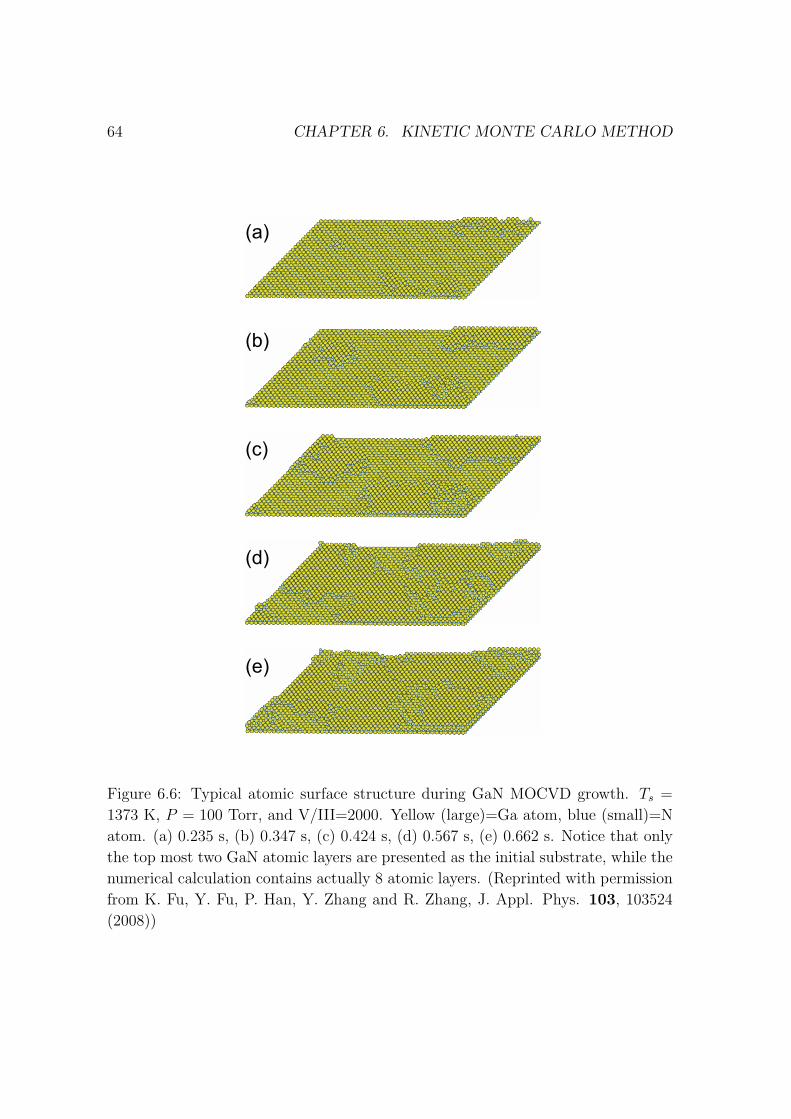
64 CHAPTER 6. KINETIC MONTE CARLO METHOD
(a)
(b)
(c)
(d)
(e)
Figure 6.6: Typical atomic surface structure during GaN MOCVD growth. Ts =
1373 K, P = 100 Torr, and V/III=2000. Yellow (large)=Ga atom, blue (small)=N
atom. (a) 0.235 s, (b) 0.347 s, (c) 0.424 s, (d) 0.567 s, (e) 0.662 s. Notice that only
the top most two GaN atomic layers are presented as the initial substrate, while the
numerical calculation contains actually 8 atomic layers. (Reprinted with permission
from K. Fu, Y. Fu, P. Han, Y. Zhang and R. Zhang, J. Appl. Phys. 103, 103524
(2008))
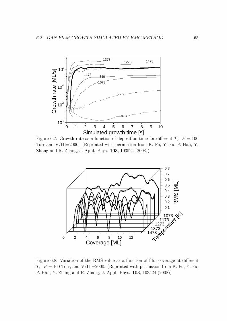
6.2. GAN FILM GROWTH SIMULATED BY KMC METHOD 65
0 1 2 3 4 5 6 7 8 9 1010-3
10-2
10-1
100
G
row
th r
ate
[ML/
s]
Simulated growth time [s]
773
840
973
1073
1173
12731373 1473
Figure 6.7: Growth rate as a function of deposition time for different Ts. P = 100
Torr and V/III=2000. (Reprinted with permission from K. Fu, Y. Fu, P. Han, Y.
Zhang and R. Zhang, J. Appl. Phys. 103, 103524 (2008))
0 2 4 6 8 10 12
0.1
0.2
0.3
0.4
0.5
0.6
0.7
0.8
Tempe
ratu
re [K
]
Coverage [ML]
RM
S [M
L]
14731373
12731173
1073
Figure 6.8: Variation of the RMS value as a function of film coverage at different
Ts. P = 100 Torr, and V/III=2000. (Reprinted with permission from K. Fu, Y. Fu,
P. Han, Y. Zhang and R. Zhang, J. Appl. Phys. 103, 103524 (2008))
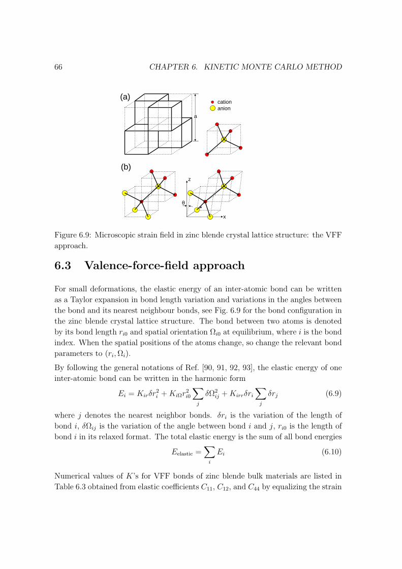
66 CHAPTER 6. KINETIC MONTE CARLO METHOD
cationanion
a
θ
z
x
(b)
(a)
Figure 6.9: Microscopic strain field in zinc blende crystal lattice structure: the VFF
approach.
6.3 Valence-force-field approach
For small deformations, the elastic energy of an inter-atomic bond can be written
as a Taylor expansion in bond length variation and variations in the angles between
the bond and its nearest neighbour bonds, see Fig. 6.9 for the bond configuration in
the zinc blende crystal lattice structure. The bond between two atoms is denoted
by its bond length ri0 and spatial orientation Ωi0 at equilibrium, where i is the bond
index. When the spatial positions of the atoms change, so change the relevant bond
parameters to (ri, Ωi).
By following the general notations of Ref. [90, 91, 92, 93], the elastic energy of one
inter-atomic bond can be written in the harmonic form
Ei = Kirδr2i + KiΩr2
i0
∑j
δΩ2ij + Kirrδri
∑j
δrj (6.9)
where j denotes the nearest neighbor bonds. δri is the variation of the length of
bond i, δΩij is the variation of the angle between bond i and j, ri0 is the length of
bond i in its relaxed format. The total elastic energy is the sum of all bond energies
Eelastic =∑
i
Ei (6.10)
Numerical values of K’s for VFF bonds of zinc blende bulk materials are listed in
Table 6.3 obtained from elastic coefficients C11, C12, and C44 by equalizing the strain
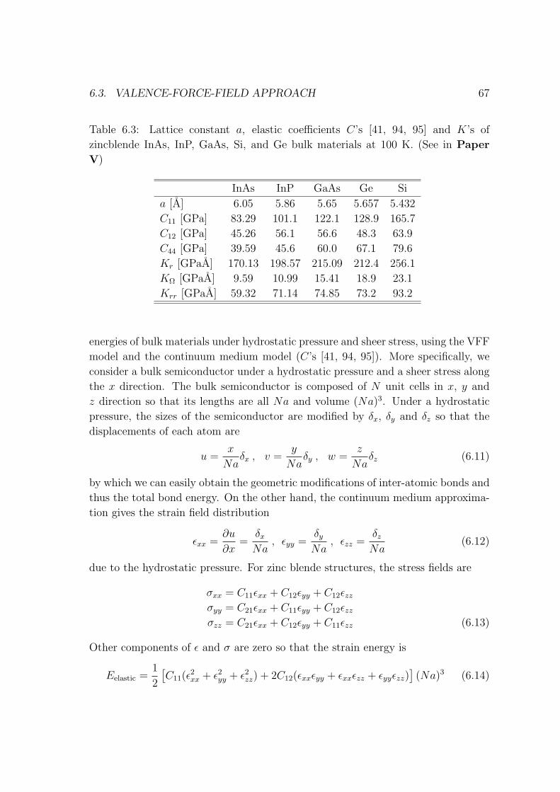
6.3. VALENCE-FORCE-FIELD APPROACH 67
Table 6.3: Lattice constant a, elastic coefficients C’s [41, 94, 95] and K’s of
zincblende InAs, InP, GaAs, Si, and Ge bulk materials at 100 K. (See in Paper
V)
InAs InP GaAs Ge Si
a [A] 6.05 5.86 5.65 5.657 5.432
C11 [GPa] 83.29 101.1 122.1 128.9 165.7
C12 [GPa] 45.26 56.1 56.6 48.3 63.9
C44 [GPa] 39.59 45.6 60.0 67.1 79.6
Kr [GPaA] 170.13 198.57 215.09 212.4 256.1
KΩ [GPaA] 9.59 10.99 15.41 18.9 23.1
Krr [GPaA] 59.32 71.14 74.85 73.2 93.2
energies of bulk materials under hydrostatic pressure and sheer stress, using the VFF
model and the continuum medium model (C’s [41, 94, 95]). More specifically, we
consider a bulk semiconductor under a hydrostatic pressure and a sheer stress along
the x direction. The bulk semiconductor is composed of N unit cells in x, y and
z direction so that its lengths are all Na and volume (Na)3. Under a hydrostatic
pressure, the sizes of the semiconductor are modified by δx, δy and δz so that the
displacements of each atom are
u =x
Naδx , v =
y
Naδy , w =
z
Naδz (6.11)
by which we can easily obtain the geometric modifications of inter-atomic bonds and
thus the total bond energy. On the other hand, the continuum medium approxima-
tion gives the strain field distribution
εxx =∂u
∂x=
δx
Na, εyy =
δy
Na, εzz =
δz
Na(6.12)
due to the hydrostatic pressure. For zinc blende structures, the stress fields are
σxx = C11εxx + C12εyy + C12εzz
σyy = C21εxx + C11εyy + C12εzz
σzz = C21εxx + C12εyy + C11εzz (6.13)
Other components of ε and σ are zero so that the strain energy is
Eelastic =1
2
[C11(ε
2xx + ε2
yy + ε2zz) + 2C12(εxxεyy + εxxεzz + εyyεzz)
](Na)3 (6.14)
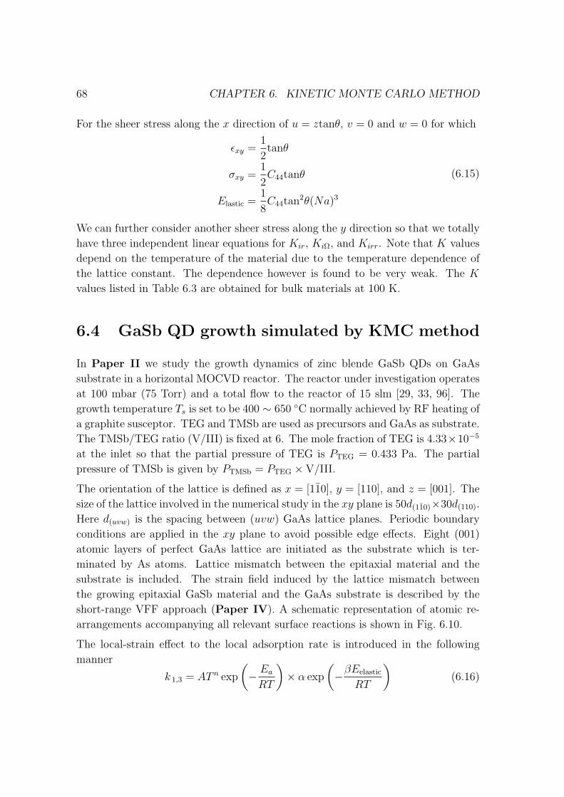
68 CHAPTER 6. KINETIC MONTE CARLO METHOD
For the sheer stress along the x direction of u = ztanθ, v = 0 and w = 0 for which
εxy =1
2tanθ
σxy =1
2C44tanθ
Elastic =1
8C44tan2θ(Na)3
(6.15)
We can further consider another sheer stress along the y direction so that we totally
have three independent linear equations for Kir, KiΩ, and Kirr. Note that K values
depend on the temperature of the material due to the temperature dependence of
the lattice constant. The dependence however is found to be very weak. The K
values listed in Table 6.3 are obtained for bulk materials at 100 K.
6.4 GaSb QD growth simulated by KMC method
In Paper II we study the growth dynamics of zinc blende GaSb QDs on GaAs
substrate in a horizontal MOCVD reactor. The reactor under investigation operates
at 100 mbar (75 Torr) and a total flow to the reactor of 15 slm [29, 33, 96]. The
growth temperature Ts is set to be 400 ∼ 650 C normally achieved by RF heating of
a graphite susceptor. TEG and TMSb are used as precursors and GaAs as substrate.
The TMSb/TEG ratio (V/III) is fixed at 6. The mole fraction of TEG is 4.33×10⁻⁵
at the inlet so that the partial pressure of TEG is PTEG = 0.433 Pa. The partial
pressure of TMSb is given by PTMSb = PTEG × V/III.
The orientation of the lattice is defined as x = [110], y = [110], and z = [001]. The
size of the lattice involved in the numerical study in the xy plane is 50d(110)×30d(110).
Here d(uvw) is the spacing between (uvw) GaAs lattice planes. Periodic boundary
conditions are applied in the xy plane to avoid possible edge effects. Eight (001)
atomic layers of perfect GaAs lattice are initiated as the substrate which is ter-
minated by As atoms. Lattice mismatch between the epitaxial material and the
substrate is included. The strain field induced by the lattice mismatch between
the growing epitaxial GaSb material and the GaAs substrate is described by the
short-range VFF approach (Paper IV). A schematic representation of atomic re-
arrangements accompanying all relevant surface reactions is shown in Fig. 6.10.
The local-strain effect to the local adsorption rate is introduced in the following
manner
k 1,3 = AT n exp
(− Ea
RT
)× α exp
(−βEelastic
RT
)(6.16)
6.4. GASB QD GROWTH SIMULATED BY KMC METHOD 69
Reactions
S1
S2
S3
S4
S5
I
II
III
IV
SbGa
Ga
GaSb
GaSb
Ga
Ga
GaSb
Ga
SbGa
Ga
GaSb
Ga GaSb
Ga
Ga
GaSb
Ga Ga
GaSb
Sb Sb
GaSb
GaSb
Sb Sb
GaSb
GaSb
Sb SbGa
Sb SbGa
Sb
Sb SbGa
Sb Sb
GaSb
Sb Sb
GaSb Sb
+ Sb
Ga+ SbSbGa
Sb SbSb Sb
SbGa
Ga
GaSb
Ga Ga+ Ga
SbGa Ga
Ga+ SbGa
Ga
Ga
Figure 6.10: Atomic rearrangements accompanying the five surface reactions listed
in Table 6.1. (Reprinted with permission from K. Fu and Y. Fu, Appl. Phys. Lett.
93, 101906 (2008))
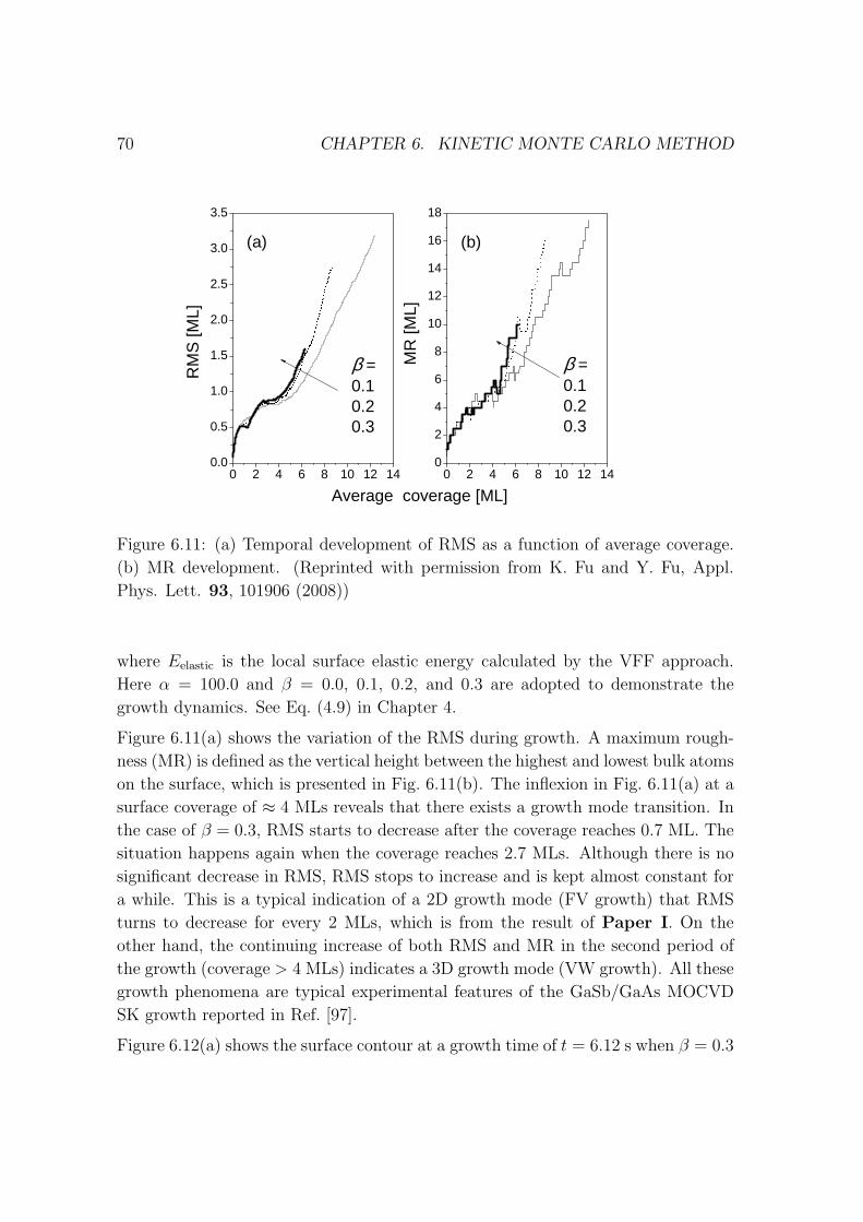
70 CHAPTER 6. KINETIC MONTE CARLO METHOD
0 2 4 6 8 10 12 140.0
0.5
1.0
1.5
2.0
2.5
3.0
3.5
0 2 4 6 8 10 12 140
2
4
6
8
10
12
14
16
18
β =0.10.20.3
RM
S [M
L]
Average coverage [ML]
(a)
MR
[ML]
β =0.10.20.3
(b)
Figure 6.11: (a) Temporal development of RMS as a function of average coverage.
(b) MR development. (Reprinted with permission from K. Fu and Y. Fu, Appl.
Phys. Lett. 93, 101906 (2008))
where Eelastic is the local surface elastic energy calculated by the VFF approach.
Here α = 100.0 and β = 0.0, 0.1, 0.2, and 0.3 are adopted to demonstrate the
growth dynamics. See Eq. (4.9) in Chapter 4.
Figure 6.11(a) shows the variation of the RMS during growth. A maximum rough-
ness (MR) is defined as the vertical height between the highest and lowest bulk atoms
on the surface, which is presented in Fig. 6.11(b). The inflexion in Fig. 6.11(a) at a
surface coverage of ≈ 4 MLs reveals that there exists a growth mode transition. In
the case of β = 0.3, RMS starts to decrease after the coverage reaches 0.7 ML. The
situation happens again when the coverage reaches 2.7 MLs. Although there is no
significant decrease in RMS, RMS stops to increase and is kept almost constant for
a while. This is a typical indication of a 2D growth mode (FV growth) that RMS
turns to decrease for every 2 MLs, which is from the result of Paper I. On the
other hand, the continuing increase of both RMS and MR in the second period of
the growth (coverage > 4 MLs) indicates a 3D growth mode (VW growth). All these
growth phenomena are typical experimental features of the GaSb/GaAs MOCVD
SK growth reported in Ref. [97].
Figure 6.12(a) shows the surface contour at a growth time of t = 6.12 s when β = 0.3
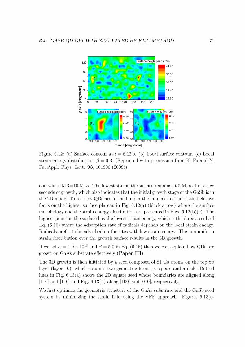
6.4. GASB QD GROWTH SIMULATED BY KMC METHOD 71
0 30 60 90 120 150 180 2100
30
60
90
120
y ax
is [a
ngst
rom
]
16.30
23.40
30.50
37.60
44.70
Surfece height [angstrom]
(a)
150 160 170 180 19050
60
70
80
90
x axis [angstrom]
18.90
26.50
34.09
40.60
(b)
150 160 170 180 19050
60
70
80
90 Strain energy [arb. unit]
4.500
43.00
81.50
114.5
(c)
Surface height [angstrom]
Figure 6.12: (a) Surface contour at t = 6.12 s. (b) Local surface contour. (c) Local
strain energy distribution. β = 0.3. (Reprinted with permission from K. Fu and Y.
Fu, Appl. Phys. Lett. 93, 101906 (2008))
and where MR=10 MLs. The lowest site on the surface remains at 5 MLs after a few
seconds of growth, which also indicates that the initial growth stage of the GaSb is in
the 2D mode. To see how QDs are formed under the influence of the strain field, we
focus on the highest surface plateau in Fig. 6.12(a) (black arrow) where the surface
morphology and the strain energy distribution are presented in Figs. 6.12(b)(c). The
highest point on the surface has the lowest strain energy, which is the direct result of
Eq. (6.16) where the adsorption rate of radicals depends on the local strain energy.
Radicals prefer to be adsorbed on the sites with low strain energy. The non-uniform
strain distribution over the growth surface results in the 3D growth.
If we set α = 1.0× 10¹³ and β = 5.0 in Eq. (6.16) then we can explain how QDs are
grown on GaAs substrate effectively (Paper III).
The 3D growth is then initiated by a seed composed of 81 Ga atoms on the top Sb
layer (layer 10), which assumes two geometric forms, a square and a disk. Dotted
lines in Fig. 6.13(a) shows the 2D square seed whose boundaries are aligned along
[110] and [110] and Fig. 6.13(b) along [100] and [010], respectively.
We first optimize the geometric structure of the GaAs substrate and the GaSb seed
system by minimizing the strain field using the VFF approach. Figures 6.13(a-
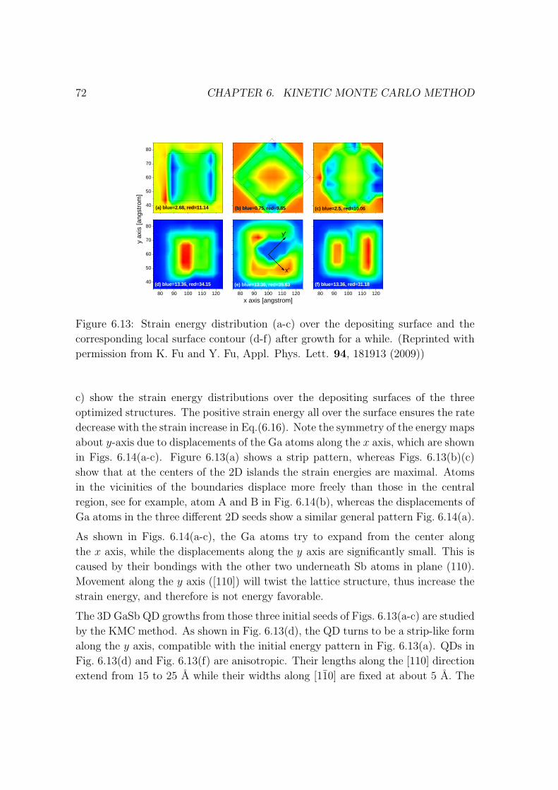
72 CHAPTER 6. KINETIC MONTE CARLO METHOD
40
50
60
70
80
y ax
is [a
ngst
rom
]
(a) blue=2.68, red=11.14
(b) blue=0.75, red=9.85 (c) blue=2.5, red=10.06
80 90 100 110 120
40
50
60
70
80
(d) blue=13.36, red=34.15
80 90 100 110 120
x axis [angstrom]
(e) blue=13.36, red=35.63
x'
y'
80 90 100 110 120
(f) blue=13.36, red=31.18
Figure 6.13: Strain energy distribution (a-c) over the depositing surface and the
corresponding local surface contour (d-f) after growth for a while. (Reprinted with
permission from K. Fu and Y. Fu, Appl. Phys. Lett. 94, 181913 (2009))
c) show the strain energy distributions over the depositing surfaces of the three
optimized structures. The positive strain energy all over the surface ensures the rate
decrease with the strain increase in Eq.(6.16). Note the symmetry of the energy maps
about y-axis due to displacements of the Ga atoms along the x axis, which are shown
in Figs. 6.14(a-c). Figure 6.13(a) shows a strip pattern, whereas Figs. 6.13(b)(c)
show that at the centers of the 2D islands the strain energies are maximal. Atoms
in the vicinities of the boundaries displace more freely than those in the central
region, see for example, atom A and B in Fig. 6.14(b), whereas the displacements of
Ga atoms in the three different 2D seeds show a similar general pattern Fig. 6.14(a).
As shown in Figs. 6.14(a-c), the Ga atoms try to expand from the center along
the x axis, while the displacements along the y axis are significantly small. This is
caused by their bondings with the other two underneath Sb atoms in plane (110).
Movement along the y axis ([110]) will twist the lattice structure, thus increase the
strain energy, and therefore is not energy favorable.
The 3D GaSb QD growths from those three initial seeds of Figs. 6.13(a-c) are studied
by the KMC method. As shown in Fig. 6.13(d), the QD turns to be a strip-like form
along the y axis, compatible with the initial energy pattern in Fig. 6.13(a). QDs in
Fig. 6.13(d) and Fig. 6.13(f) are anisotropic. Their lengths along the [110] direction
extend from 15 to 25 A while their widths along [110] are fixed at about 5 A. The
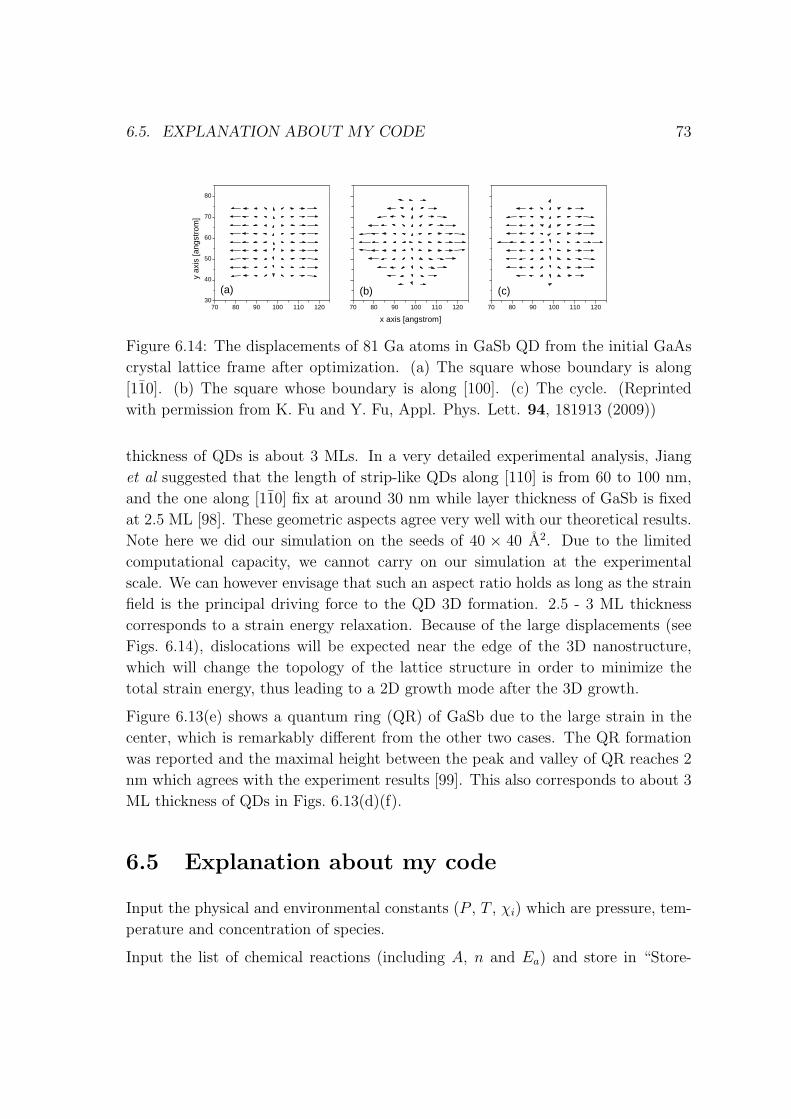
6.5. EXPLANATION ABOUT MY CODE 73
70 80 90 100 110 12030
40
50
60
70
80
(a)
y ax
is [a
ngst
rom
]
70 80 90 100 110 120
x axis [angstrom]
(b)70 80 90 100 110 120
(c)
Figure 6.14: The displacements of 81 Ga atoms in GaSb QD from the initial GaAs
crystal lattice frame after optimization. (a) The square whose boundary is along
[110]. (b) The square whose boundary is along [100]. (c) The cycle. (Reprinted
with permission from K. Fu and Y. Fu, Appl. Phys. Lett. 94, 181913 (2009))
thickness of QDs is about 3 MLs. In a very detailed experimental analysis, Jiang
et al suggested that the length of strip-like QDs along [110] is from 60 to 100 nm,
and the one along [110] fix at around 30 nm while layer thickness of GaSb is fixed
at 2.5 ML [98]. These geometric aspects agree very well with our theoretical results.
Note here we did our simulation on the seeds of 40 × 40 A2. Due to the limited
computational capacity, we cannot carry on our simulation at the experimental
scale. We can however envisage that such an aspect ratio holds as long as the strain
field is the principal driving force to the QD 3D formation. 2.5 - 3 ML thickness
corresponds to a strain energy relaxation. Because of the large displacements (see
Figs. 6.14), dislocations will be expected near the edge of the 3D nanostructure,
which will change the topology of the lattice structure in order to minimize the
total strain energy, thus leading to a 2D growth mode after the 3D growth.
Figure 6.13(e) shows a quantum ring (QR) of GaSb due to the large strain in the
center, which is remarkably different from the other two cases. The QR formation
was reported and the maximal height between the peak and valley of QR reaches 2
nm which agrees with the experiment results [99]. This also corresponds to about 3
ML thickness of QDs in Figs. 6.13(d)(f).
6.5 Explanation about my code
Input the physical and environmental constants (P , T , χi) which are pressure, tem-
perature and concentration of species.
Input the list of chemical reactions (including A, n and Ea) and store in “Store-
74 CHAPTER 6. KINETIC MONTE CARLO METHOD
TypeRate”.
Assign topological positions (ijk) and space positions (xyz) for lattice sites. There
are 50× 30 atoms in xy plane and totally 100 monolayer in the z direction.
Assign neighbors for each lattice site.
Initiate the substrate. Fill atoms into the monolayers in the basement of the struc-
ture. For GaN growth, terminate the surface with NH3. Set time to zero.
For each lattice site, set the reaction rates if available.
For each simulation step, pick one reaction of certain site and do the event. After
that, update the configuration of the structure.
Next simulation step till end.
Function to do reaction event (including the module Adsorb, Desorb, GaLoop, and
SbLoop)
For each event, n in the event list
Add the rate of event n to totalReactionRate: totalReactionRate +=rn.
Next n.
Pick a random number, ξ1 ∈ (0, 1).
Update the simulation clock: t+ = dt = −ln(ξ1)/totalReactionRate
Pick another random number, ξ2 ∈ (0, 1).
Find the event N ifN−1∑n=0
rn/totalReactionRate ≤ ξ2 <N∑
n=0
rn/totalReactionRate
Record the reaction J and the site I, which correspond to event N .
If reaction J is MMG deposition at site I then AdsorbMMGa(I).
Else if reaction J is NH3 deposition at site I then AdsorbNH3(I).
Else if reaction J is decomposition of NH3 at site I then DecomposeNHx(I)
Else if reaction J is H etching at site I then AbstractH(I)
Else if reaction J is desorption of CH3 at site I then DesorbCH3(I)
Else if reaction J is desorption of NH3 at site I then DesorbNH3(I)
Else if reaction J is desorption of MMG at site I then DesorbMMGa(I)
Else if reaction J is final deposition of GaN at site I then Loop(I).
For each lattice site, s, that was modified by the reaction at site I, remove all events
6.5. EXPLANATION ABOUT MY CODE 75
for site I from the event list. Specifically if we add VFF module which could help
us calculate the local strain energy and optimize the configurations of the local
structure, the first neighbors or the second nearest neighbors of the site I will be
reorganized for their space positions.
Add all the reaction at site s into the event list
Next s
End functions to do reaction event.
Functions to judge types of reactions j available at site i.
If reaction j occur at site i, then
If reaction j is about MMG deposition at site i then:
if site i is filled with nitrogen, and at one of the three directions above there is an
empty site for MMG (there are three Ga atoms above connected with nitrogen).
Meanwhile at this direction the bond of the nitrogen is broken (not terminated by
H or other atoms), then Return(yes). Else Return(no).
Else if reaction j is NH3 deposition at site i then
if site i is filled with Ga, and above is an empty site for NH3. Meanwhile at this
direction the bond of Ga is broken (not terminated by CH3 or other atoms), then
Return(yes). Else Return(no).
Else if reaction j is decomposition of NH3 or about H etching at site i then
if at least at one of the three directions above, the site i (filled with nitrogen) is
connected with H atom, then Return(yes). Else Return(no).
Else if reaction j is desorption of CH3 at site i then
if site i is filled with Ga, and above is a radical CH3, then Return(yes). Else
Return(no).
Else if reaction j is desorption of NH3 at site i then
if site i is filled with NH3, then Return(yes). Else Return(no).
Else if reaction j is desorption of MMG at site i then
if site i is filled with MMG, then Return(yes). Else Return(no).
Else if reaction j is about final deposition of GaN at site i then
if only at site i, the “hexagon” of GaN has a broken bond, which means other five
bonds are all connected, then Return(yes). Else Return(no).

76 CHAPTER 6. KINETIC MONTE CARLO METHOD
End functions to judge types of reactions.
Function AdsorbMMGa(I)
change site I from a radical to a Ga atom and meanwhile fill the lattice sites above
with CH3 and fill the other two empty neighbors with radicals.
End function
Function AdsorbNH3(I)
change site I from a radical to a N atom and meanwhile fill the three lattice sites
above with H atoms.
End function
Function DecomposeNHx(I)
For site I remove one of the neighbors which should be occupied by H atom.
End function
Function DesorbCH3(I)
remove CH3 at site I
End function
Function DesorbNH3(I)
remove N atom at site I and meanwhile remove the three H atoms above.
End function
Function DesorbMMGa(I)
remove Ga atom at site I and meanwhile remove CH3 above and the radicals at the
other two neighbors.
End function
Function Loop(I)
First find out the broken bond at site I and make it a bond. Then make all the atoms
in the hexagon be the crystal atoms which are totally different from the adsorbed
atoms.
End function
Chapter 7
Comments on included papers
• Paper 1: Kinetic Monte Carlo study of MOCVD growth dynamics of GaN thin
film at microscopic level
In this work, by combining the CFD and KMC methods, we present a mul-
tiscale modeling of fluid dynamics, thermodynamics, and MD to study the
chemical and physical growth process of GaN in a standard MOCVD reactor,
which shows a general agreement with experimental results. The dynamic
evolution of the epitaxial growth is studied using the basic framework of the
KMC method of Battaile. And the CFD simulation is based on the mul-
tiphysics solver CFD-ACE+. The theoretical model thus provides us with a
fundamental guideline for optimizing GaN MOCVD growth at the microscopic
level. It has been found that at a high temperature of Ts ≥ 1073 K, the ho-
moepitaxial film grows in a 2D step mode. At the optimized temperature of
Ts = 1373 K, the film growth has a fast growth rate with a relatively low
nuclear density. The quality of the film is expected to be best at this growth
temperature, which agrees well with the experimental discoveries.
• Paper 2: Kinetic Monte Carlo study of metal organic chemical vapour deposi-
tion growth mechanism of GaSb quantum dots
In this paper, the growth dynamics of self-assembled GaSb QDs on GaAs sub-
strate in the strain-induced SK mode was investigated using KMC method.
The strain field induced by the lattice mismatch between the growing epitaxial
GaSb material and the GaAs substrate is described by the short-range VFF
77
78 CHAPTER 7. COMMENTS ON INCLUDED PAPERS
approach. The strain was shown to be directly responsible for the QD forma-
tion and the transition of growth mode from 2D to 3D. The statistics of the
spatial separations between adjacent atomic layers along the z axis shows that
the strain energy along the z axis is partially released during the growth.
• Paper 3: Growth dynamics of GaSb quantum dots in strain-induced Stranski-
Krastanov mode
In this work, we studied the growth dynamics of GaSb QDs on GaAs substrate
by advanced quantum mechanics. The strain-aided formation of QDs in the
SK mode has been clearly revealed: Without taking into account the strain
field the growth of GaSb material on GaAs is in the 2D layer-by-layer mode.
The strain induced by the lattice mismatch between the epitaxial material
and the substrate is directly responsible for the QD formation which is energy
favourable.
• Paper 4: Strain-induced Stranski-Krastanov three-dimensional growth mode of
GaSb quantum dot on GaAs substrate
In this work, the growth dynamics of self-assembled GaSb QDs on GaAs sub-
strate was investigated using KMC method. The strain induced by the lattice
mismatch between the epitaxial material and the substrate was shown to be
directly responsible for the three dimensional QD formation. I have studied
the relationship between the local strain energy and local displacement for the
atoms in the QD. Different geometries of the initial seeds on the surface which
are equally favorable from an energy point of view can result in different GaSb
nanostructures (nanostrips and nanoring).
• Paper 5: Strain effect in determining the geometric shape of self-assembled
quantum dot
The geometric shape of a self-assembled QD formed by the strain-induced
SK mode has been studied as a function of strain energy by the short-range
VFF approach. It has been shown by dynamic bond relaxation through strain
energy minimization that for the most commonly used InAs QD in GaAs and
InP matrices and Ge QD in Si matrix, a pyramidal shape is energy favoured
over an hemispherical shape when the QD is not capped due to the lattice
relaxation at the QD surface. When the QD becomes totally embedded in
79
the background material, the elastic strain energy of a hemispherical InAs QD
is minimal. The results agree with experimental observations. We further
studied the coupling of strain fields of QDs in adjacent QD layers which shows
that QDs in multiply stacked QD layers can be aligned along the layer growth
direction in order to minimize the strain energy.
• Paper 6: Kinetic Monte Carlo study of stacked GaSb quantum dot MOCVD
growth
Strain-induced self assembly of stacking GaSb QDs in GaAs matrix by MOCVD
method has been studied by KMC method coupled with lattice-mismatch in-
duced strain. Our study shows that on the surface of a GaAs substrate already
embedded with a buried GaSb QD, the growth of the top GaSb QD is largely
determined by the strain field distribution on the growth surface due to the
buried GaSb QD. When the distance from the buried GaSb QD to the growth
surface is small, the modulation in the strain energy distribution on the growth
surface is large, resulting in a 3D GaSb QD growth mode with a fast growth
rate and a large aspect ratio. When the distance is large, the surface growth
starts with a 2D layer-by-layer mode with a slow growth rate and a low aspect
ratio.

80 CHAPTER 7. COMMENTS ON INCLUDED PAPERS
Bibliography
[1] http://www.sia-online.org/cs/industry resources/industry fact sheet.
[2] T.-T. Han, Y. Fu, H. Agren, P. Han, Z. Qin, and R. Zhang, Appl. Phys. A,
86, 145 (2006).
[3] H. Kirmse, R. Schneider, M. Rabe, W. Neumann, and F. Henneberger, Appl.
Phys. Lett. 72, 1329 (1998).
[4] S. Lee, I. Daruka, C. S. Kim, A. L. Barabasi, J. L. Merz, and J. K. Furdyna,
Phys. Rev. Lett. 81, 3479 (1998).
[5] M. C. Tamargo, II-VI semiconductor materials and their applications, CRC
Press, 2002.
[6] Y. Fu. S. Hellstrom, and H. Agren, Journal of Nonlinear Optical Physics &
Materials (JNOPM), 18, 195 (2009).
[7] M. R. Krames, O. B. Shchekin, R. Mueller-Mach, G. O. Mueller, L. Zhou, G.
Harbers, and M. George Craford, J. Disp. Technol., 3, 160 (2007).
[8] S. Nakamura, M. Senoh, S. Nagahama, N. Iwasa, T. Yamada, T. Matsushita,
H. Kiyoku, Y. Sugimoto, T. Kozaki , H. Umemoto and K. Chocho, Appl. Phys.
Lett. 72, 2014 (1998).
[9] B. Monemar, G. Pozina, Prog. Quantum Electron., 24, 239 (2000).
[10] J. W. Orton and C. T. Foxon, Rep. Prog. Phys. 61, 1 (1998).
[11] C. Yang, X. Wang, H. Xiao, X. Zhang, G. Hu, J. Ran, C. Wang, J. Li, J. Li
and Z. Wang, Appli. Surf. Sci. 255, 3149 (2008).
[12] H. N. G. Wadley, X. Zhou, R. A. Johnson and M. Neurock, Progr. Mater. Sci.
46, 329 (2001)
81
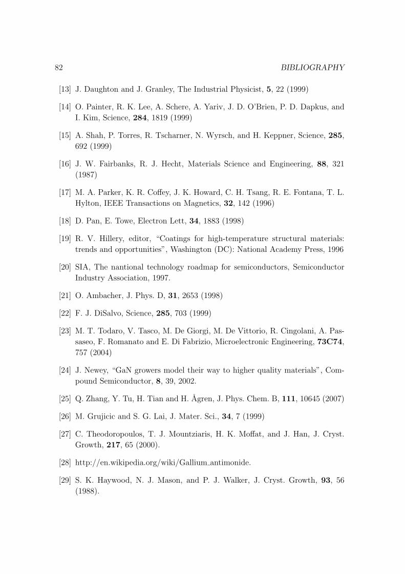
82 BIBLIOGRAPHY
[13] J. Daughton and J. Granley, The Industrial Physicist, 5, 22 (1999)
[14] O. Painter, R. K. Lee, A. Schere, A. Yariv, J. D. O’Brien, P. D. Dapkus, and
I. Kim, Science, 284, 1819 (1999)
[15] A. Shah, P. Torres, R. Tscharner, N. Wyrsch, and H. Keppner, Science, 285,
692 (1999)
[16] J. W. Fairbanks, R. J. Hecht, Materials Science and Engineering, 88, 321
(1987)
[17] M. A. Parker, K. R. Coffey, J. K. Howard, C. H. Tsang, R. E. Fontana, T. L.
Hylton, IEEE Transactions on Magnetics, 32, 142 (1996)
[18] D. Pan, E. Towe, Electron Lett, 34, 1883 (1998)
[19] R. V. Hillery, editor, “Coatings for high-temperature structural materials:
trends and opportunities”, Washington (DC): National Academy Press, 1996
[20] SIA, The nantional technology roadmap for semiconductors, Semiconductor
Industry Association, 1997.
[21] O. Ambacher, J. Phys. D, 31, 2653 (1998)
[22] F. J. DiSalvo, Science, 285, 703 (1999)
[23] M. T. Todaro, V. Tasco, M. De Giorgi, M. De Vittorio, R. Cingolani, A. Pas-
saseo, F. Romanato and E. Di Fabrizio, Microelectronic Engineering, 73C74,
757 (2004)
[24] J. Newey, “GaN growers model their way to higher quality materials”, Com-
pound Semiconductor, 8, 39, 2002.
[25] Q. Zhang, Y. Tu, H. Tian and H. Agren, J. Phys. Chem. B, 111, 10645 (2007)
[26] M. Grujicic and S. G. Lai, J. Mater. Sci., 34, 7 (1999)
[27] C. Theodoropoulos, T. J. Mountziaris, H. K. Moffat, and J. Han, J. Cryst.
Growth, 217, 65 (2000).
[28] http://en.wikipedia.org/wiki/Gallium antimonide.
[29] S. K. Haywood, N. J. Mason, and P. J. Walker, J. Cryst. Growth, 93, 56
(1988).
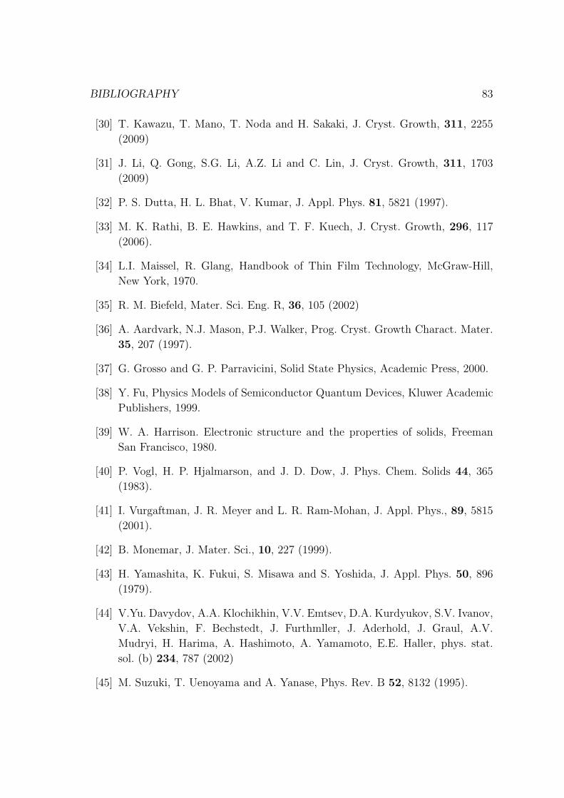
BIBLIOGRAPHY 83
[30] T. Kawazu, T. Mano, T. Noda and H. Sakaki, J. Cryst. Growth, 311, 2255
(2009)
[31] J. Li, Q. Gong, S.G. Li, A.Z. Li and C. Lin, J. Cryst. Growth, 311, 1703
(2009)
[32] P. S. Dutta, H. L. Bhat, V. Kumar, J. Appl. Phys. 81, 5821 (1997).
[33] M. K. Rathi, B. E. Hawkins, and T. F. Kuech, J. Cryst. Growth, 296, 117
(2006).
[34] L.I. Maissel, R. Glang, Handbook of Thin Film Technology, McGraw-Hill,
New York, 1970.
[35] R. M. Biefeld, Mater. Sci. Eng. R, 36, 105 (2002)
[36] A. Aardvark, N.J. Mason, P.J. Walker, Prog. Cryst. Growth Charact. Mater.
35, 207 (1997).
[37] G. Grosso and G. P. Parravicini, Solid State Physics, Academic Press, 2000.
[38] Y. Fu, Physics Models of Semiconductor Quantum Devices, Kluwer Academic
Publishers, 1999.
[39] W. A. Harrison. Electronic structure and the properties of solids, Freeman
San Francisco, 1980.
[40] P. Vogl, H. P. Hjalmarson, and J. D. Dow, J. Phys. Chem. Solids 44, 365
(1983).
[41] I. Vurgaftman, J. R. Meyer and L. R. Ram-Mohan, J. Appl. Phys., 89, 5815
(2001).
[42] B. Monemar, J. Mater. Sci., 10, 227 (1999).
[43] H. Yamashita, K. Fukui, S. Misawa and S. Yoshida, J. Appl. Phys. 50, 896
(1979).
[44] V.Yu. Davydov, A.A. Klochikhin, V.V. Emtsev, D.A. Kurdyukov, S.V. Ivanov,
V.A. Vekshin, F. Bechstedt, J. Furthmller, J. Aderhold, J. Graul, A.V.
Mudryi, H. Harima, A. Hashimoto, A. Yamamoto, E.E. Haller, phys. stat.
sol. (b) 234, 787 (2002)
[45] M. Suzuki, T. Uenoyama and A. Yanase, Phys. Rev. B 52, 8132 (1995).
84 BIBLIOGRAPHY
[46] M.C. Wu and C.C. Chen, J. Appl. Phys. 72, 9, 4275 (1992).
[47] R. Timm, A. Lenz, H. Eisele, L. Ivanova, M. Dahne, G. Balakrishnan, D. L.
Huffaker, I. Farrer, and D. A. Ritchie, J. Vac. Sci. Technol. B, 26, 1492 (2008).
[48] M. Geller, C. Kapteyn, L. Muller-Kirsch, R. Heitz, and D. Bimberg, Appl.
Phys. Letts. 82, 2706 (2003).
[49] “Wide bandgap semiconductors: fundamental properties and modern photonic
and electronic devices”. Edited by K. Takahashi, A. Yoshikawa and A. Sandhu,
Springer, 2007.
[50] N. S. Saks, A. Edwards, J. M. Redwing, A. E. Wickenden and D. D. Koleske,
Proceedings of the Second International Conferences on Nitride Semiconduc-
tors, Tokushima, Japan, 476, 1997.
[51] “WIDE - World Market For Wide Bandgap Materials And Devices For RF
Applications” by Yole Developpement, 2005
[52] M. Asif Khan, J. N. Kuznia, A. R. Bhattarai, and D. T. Olson, Appl. Phys.
Lett. 62, 1786 (1993)
[53] V. Cimalla, J. Pezoldt and O. Ambacher, J. Phys. D, 40, 6386 (2007).
[54] “Quantum dots”, edited by E. Borovitskaya and M. S. Shur, World Scientific,
New Jersey, 2002.
[55] Y. Nakamura, T. Sugimoto, and M. Ichikawa, J. Appl. Phys. 105, 014308
(2009).
[56] A. D. Yoffe, Adv. Phys., 50, 1 (2001)
[57] X. Michalet, F. F. Pinaud, L. A. Bentolila, J. M. Tsay, S. Doose, J. J. Li, G.
Sundaresan, A. M. Wu, S. S. Gambhir, and S. Weiss, Science, 307, 538 (2005)
[58] N. Yamamoto, K. Akahane, S. Gozu, A. Ueta, N. Ohtani, and M. Tsuchiya,
Jpn. J. Appl. Phys. 46, 2401 (2007).
[59] M. Geller, A. Marent, T. Nowozin, D. Bimberg, N. Akcay, and N. Oncan,
Appl. Phys. Lett. 92, 092108 (2008)
[60] S. Nakamura, Jpn. J. Appl. Phys. Part 2, 30, L1705 (1991)
BIBLIOGRAPHY 85
[61] E. J. Tarsa, B. Heying, X. H. Wu, P. Fini, S. P. DenBaars, and J. S. Speck,
J. Appl. Phys., 82, 5472 (1997)
[62] H. Marchand, J. P. Ibbetson, P. T. Fini, P. Kozodoy, S. Keller, S. DenBaars,
J. S. Speck, and U. K. Mishra, MRS Internet J. Nitride Semicond. Res., 3, 3
(1998)
[63] K.-J. Choi, W.-C. Shin, and S.-G. Yoon, J. Electrochem. Soc. 149, F18 (2002).
[64] K. Nishikata, H. Shimizu, K. Hiraiwa, S. Yoshida, N. Yamanaka, M. Irikawa,
A. Kasukawa, J. Cryst. Growth, 175, 990 (1997)
[65] D. Sengupta, S. Mazumder, W. Kuykendall, and S. A. Lowry, J. Cryst.
Growth, 279, 369 (2005).
[66] T. G. Mihopoulos, “Reaction and transport processes in MOCVD selective and
group III-Nitride growth”, Ph. D. Thesis, Massachusetts Institute of Technol-
ogy, 1999.
[67] D. Moscatelli, P. Caccioppoli, and C. Cavallotti, Appl. Phys. Lett. 86, 091106
(2005).
[68] F. Jensen, Introduction to Computational Chemistry, Wiley, 1999.
[69] I. N. Levine, Quantum Chemistry, the fifth edition, Prentice Hall, 2000.
[70] K. Kusakabe, A. Hirako, S. Tanaka, and K. Ohkawa, Phys. Stat. Sol. (c), 1,
2569 (2004).
[71] A. Hirako, K. Kusakabe, and K. Ohkawa, Jpn. J. Appl. Phys. 44, 874 (2005).
[72] R. P. Parikh and R. A. Adomaitis, J. Cryst. Growth, 286, 259 (2006).
[73] R. P. Parikh, R. A. Adomaitis, M. E. Aumer, D. P. Partlow, D. B. Thomson,
and G. W. Rubloff, J. Cryst. Growth, 296, 15 (2006).
[74] R. P. Pawlowski, C. Theodoropoulos, A. G. Salinger, T. J. Mountziaris, H. K.
Moffat, J. N. Shadid, and E. J. Thrush, J. Cryst. Growth, 221, 622 (2000).
[75] S. Mazumder and S. A. Lowry, J. Cryst. Growth, 224, 165 (2001).
[76] H. Morko and H. Morkoa, Nitride Semiconductors and Devices, Springer, 2009.
[77] D. A. Neumayer and J. G. Ekerdt, Chem. Mater. 8, 9 (1996).
86 BIBLIOGRAPHY
[78] R. Niebuhr, K. Bachem, K. Dombrowski, M. Maier, W. Pletschen and U.
Kaufmann, Journal of Electronic Materials, 24, 1531 (1995)
[79] I. V. Markov, “Crystal Growth for Beginners: Fundamentals of Nucleation,
Crystal Growth, and Epitaxy.” Singapore: World, 1995. Scientific.
[80] R. Chang, “Chemistry (ninth edition)”, McGraw-Hill Higher Education, 2007.
[81] http://www.phys.uit.no/∼inge/ttp5/concept-of-pes.htm
[82] “CFD-ACE+ V2004 Modules Manual - Volume 1”, ESI US R&D, Inc, 2004
[83] D. G. Zhao, D. S. Jiang, J. J. Zhu, Z. S. Liu, S. M. Zhang, H. Yang and J. W.
Liang, J. Cryst. Growth, 303, 414 (2007).
[84] S. Figge, T. Bottcher, S. Einfeldt and D. Hommel, J. Cryst. Growth, 221,
262, (2000).
[85] T. Yang, K. Uchida, T. Mishima, J. Kasai and J. Gotoh, Phys. Status Solidi
(a), 180, 45, (2000).
[86] S. Kim, J. Oh, J. Kang, D. Kim, J. Won, J.W. Kim and H.K. Cho, J. Cryst.
Growth, 262, 7 (2004).
[87] M. Mizuta, S. Fujieda, Y. Matsumoto and T. Kawamura, Jpn. J. Appl. Phys.
25, L945, (1986)
[88] C. J. Weststrate, J. W. Bakker, E. D. L. Rienks, S. Lizzit, L. Petaccia, A.
Baraldi, C. P. Vinod, and B. E. Nieuwenhuys, J. Chem. Phys. 122, 184705
(2005).
[89] C. C. Battaile, D. J. Srolovitz and J. E. Butler, J. Appl. Phys. 82, 6293 (1997).
[90] M. A. Nusimovici and J. L. Birman, Phys. Rev. 156, 925 (1967).
[91] R. M. Martin, Phys. Rev. B. 1, 4005 (1970).
[92] R. Ramani, K. K. Mani, and R. P. Singh, Phys. Rev. B, 14, 2659 (1976).
[93] P. N. Keating, Phy. Rev. 145, 637 (1966).
[94] T. Ito, K. E. Khor, and S. Das Sarma, Phys. Rev. B, 40, 9715 (1989).
[95] “Semiconductors Group IV Elements and III-V Compounds”, ed. O.
Madelung, Springer-Verlag Berlin, 1991.
BIBLIOGRAPHY 87
[96] R. Timm, H. Eisele, A. Lenz, S. K. Becker, J. Grabowski, T.-Y. Kim, L.
Muller-Kirsch, K. Potschke, U. W. Pohl, D. Bimberg, and M. Dahne, Appl.
Phys. Letts. 85, 5890 (2004).
[97] L. Muller-Kirsch, R. Heitz, U. W. Pohl, D. Bimberg, I. Hausler, H. Kirmse,
and W. Neumann, Appl. Phys. Letts. 79, 1027 (2001).
[98] C. Jiang, and H. Sakaki, Physica E, 32, 17 (2006).
[99] S. Kobayashi, C. Jiang, T. Kawazu, and H. Sakaki, Jpn. J. Appl. Phys. 43,
L662 (2004).
Recommended


![SPIN CURRENTS IN SEMICONDUCTOR NANOSTRUCTURES: A ...bnikolic/PDF/spin_currents_oup.pdf · arXiv:0907.4122v1 [cond-mat.mes-hall] 23 Jul 2009 SPIN CURRENTS IN SEMICONDUCTOR NANOSTRUCTURES:](https://img.pdfslide.us/doc/110x75/5f336dbb72f2ec2b812bb7bc/spin-currents-in-semiconductor-nanostructures-a-bnikolicpdfspincurrentsouppdf.jpg)