White Paper
50V RF LDMOS An ideal RF power technology for ISM, broadcast and commercial aerospace applications
freescale.com/RFpower

2 Freescale Semiconductor, Inc.
I. INTRODUCTIONRF laterally diffused MOS (LDMOS) is currently the dominant device technology used in high-power RF power amplifier
(PA) applications for frequencies ranging from 1 MHz to greater than 3.5 GHz.
Beginning in the early 1990s, LDMOS has gained wide acceptance for cellular infrastructure PA applications, and now is
the dominant RF power device technology for cellular infrastructure.
This device technology offered significant advantages over the previous incumbent device technology, the silicon
bipolar transistor, providing superior linearity, efficiency, gain and lower cost packaging options.
LDMOS technology has continued to evolve to meet the ever more demanding requirements of the cellular
infrastructure market, achieving higher levels of efficiency, gain, power and operational frequency[1-8]. The LDMOS
device structure is highly flexible. While the cellular infrastructure market has standardized on 28–32V operation, several
years ago Freescale developed 50V processes for applications outside of cellular infrastructure. These 50V devices are
targeted for use in a wide variety of applications where high power density is a key differentiator and include industrial,
scientific, medical (ISM), broadcast and commercial aerospace applications.
Many of the same attributes that led to the displacement of bipolar transistors from the cellular infrastructure market in
the early 1990s are equally valued in the broad RF power market: high power, gain, efficiency and linearity, low cost and
outstanding reliability.
In addition, the RF power market demands the very high RF ruggedness that LDMOS can deliver. The enhanced
ruggedness LDMOS devices available from Freescale can displace not only bipolar devices but VMOS and vacuum tube
devices that are still used in some ISM, broadcast and commercial aerospace applications. The 50V devices designed
by Freescale are fabricated on Freescale’s unique very high voltage sixth-generation (VHV6) platform, and have been
fully qualified and are shipping in volume. This paper describes the basic VHV6 device structure and the enhanced
ruggedness variant (EVHV6), including advantages over competing device technologies. Ruggedness expectations and
requirements for RF power devices targeting ISM applications are more stringent than for devices designed for less
challenging applications like cellular infrastructure. This paper will include device and design considerations that specifically
target enhancing ruggedness performance. The features of the products using this platform will also be presented.
II. LDMOS DEVICE TECHNOLOGY Figure 1 depicts a cross section of
a single finger of a typical LDMOS
transistor. It includes a source metal
region to electrically connect the N+
source to the P+ sinker, which in turn
is connected to the back side source
metal through the P+ substrate. This
patented feature significantly lowers
the source inductance to improve
performance, but also allows the die to
be directly attached onto an electrically
and thermally conductive package
flange to accommodate low-cost
packaging platforms.
Figure 1: Cross section of an LDMOS device
Freescale Semiconductor, Inc. 3
The boron p-type “PHV” diffusion establishes the threshold voltage
and turn-on characteristics of the device. The WSi/polysilicon
gate provides a low gate access resistance, important for the
large dimensions typical of RF power devices. A low doping
concentration arsenic n-type “NHV” drift region between the gate
and the highly doped N+ drain region is designed to support high
breakdown voltages, low on-state resistance (RDSon) and good
hot carrier injection (HCI) reliability. The stacked aluminum drain
metal is designed to meet electromigration specifications for high
reliability. A metal-2 gate bus running parallel to the gate makes
periodic connections to the gate WSi/polysilicon stack to reduce
its resistance. Grounded shield structures (the ground strap is
not shown in this figure) are also employed to reduce feedback
capacitance between the drain and gate, and to control surface
electric fields to allow for improved device performance without
sacrificing breakdown voltage or HCI margin.
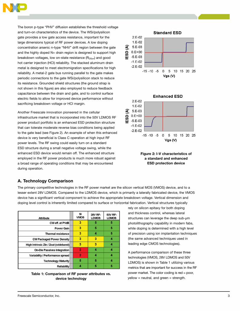
Another Freescale innovation pioneered in the cellular
infrastructure market that is incorporated into the 50V LDMOS RF
power product portfolio is an enhanced ESD protection structure
that can tolerate moderate reverse bias conditions being applied
to the gate lead (see Figure 2). An example of when this enhanced
device is very beneficial is Class C operation at high input RF
power levels. The RF swing could easily turn on a standard
ESD structure during a small negative voltage swing, while the
enhanced ESD device would remain off. The enhanced structure
employed in the RF power products is much more robust against
a broad range of operating conditions that may be encountered
during operation.
A. Technology ComparisonThe primary competitive technologies in the RF power market are the silicon vertical MOS (VMOS) device, and to a
lesser extent 28V LDMOS. Compared to the LDMOS device, which is primarily a laterally fabricated device, the VMOS
device has a significant vertical component to achieve the appropriate breakdown voltage. Vertical dimension and
doping level control is inherently limited compared to surface or horizontal fabrication. Vertical structures typically
rely on silicon epitaxy for both doping
and thickness control, whereas lateral
structures can leverage the deep sub-μm
photolithography capability in modern fabs,
while doping is determined with a high level
of precision using ion implantation techniques
(the same advanced techniques used in
leading edge CMOS technologies).
A performance comparison of these three
technologies (VMOS, 28V LDMOS and 50V
LDMOS) is shown in Table 1 utilizing various
metrics that are important for success in the RF
power market. The color coding is red = poor,
yellow = neutral, and green = strength.
Figure 2: I-V characteristics of a standard and enhanced
ESD protection device
Table 1: Comparison of RF power attributes vs. device technology

4 Freescale Semiconductor, Inc.
The scale ranges from 1 to 5, with 5 being highest, or best. Starting down the metric list, LDMOS has superior gain
and efficiency that can be traced to developments originally driven by the cellular infrastructure market where these
parameters have long been of paramount importance, along with device structure advantages such as deep sub-μm self-
aligned gates and shields to reduce feedback capacitance. The LDMOS devices have thermal resistance benefits as a
result of having a backside source that can be connected directly to the thermally and electrically conductive package
flange, which in turn is directly mounted to the heat sink. Typical VMOS devices have the drain on the backside of
the wafer and require attaching the die to an electrically isolating flange material which increases the effective thermal
resistance of this device structure. The excellent thermal conductivity of the LDMOS packaged products allows them
to achieve significantly higher continuous wave (CW) power levels in a given package, especially the 50V technology
with its inherently higher power density compared to the 28V variant. In addition, 50V LDMOS typically has 35% less
output capacitance per watt (W) than competing 50V Si technologies, making it ideal for broadband applications.
LDMOS products in the cellular infrastructure market are typically manufactured with integrated matching networks,
making the availability of on-die passives (inductors, capacitors) an LDMOS strength. The lateral nature of the LDMOS
manufacturing flow leverages fab processes that can be controlled to very high precision levels, compared to VMOS
that requires less well-controlled processes such as silicon epitaxy to form certain critical active regions of the structure,
increasing variability and performance spread. Although VMOS and LDMOS are mature device technologies, the 50V
LDMOS variant is a relative newcomer to the RF power market. Finally, LDMOS technology has a demonstrated track
record of providing outstanding reliability with nearly 20 years of widespread deployment in the demanding cellular
infrastructure market.
B. Technology Development TrendsFreescale has a unique advantage in having robust development programs for both 28V and 50V LDMOS, and in being
a leading supplier to both the cellular infrastructure market and the ISM, broadcast and commercial aerospace markets.
This cross-fertilization of development programs accelerates development in all these areas, and extends the impact of
R&D investments across a broader product space.
Several trends have emerged
over the past few years. Figure 3
highlights four that are applicable to
both cellular infrastructure as well
as the other RF power markets.
The first is increased frequency of
operation, with products already
qualified for operation up to
3.8 GHz for 28V; Freescale’s 50V
platform supports products with
frequencies exceeding 3 GHz.
The second trend is the release
of high power, multi-stage ICs, or
discrete devices with integrated
input and output matching
networks. These high-power RF
devices are common in the cellular
infrastructure market. Products are
in development for other RF power
markets that include integrated
matching networks to simplify ease
of use while maintaining broadband
performance.
Figure 3: LDMOS development trends

Freescale Semiconductor, Inc. 5
The third major trend is the adoption of over-molded plastic (OMP) for high-power RF applications. OMP is the lowest
cost packaging technology available; Freescale has a leadership position pioneering OMP for cellular infrastructure
applications, and has leveraged this experience into the RF power product portfolio. Package development within
Freescale continues, with the primary emphasis on increasing the power level that can be accommodated. The final
trend is to continue to invest heavily in 50V LDMOS development for the RF power market.
III. RUGGEDNESS ENHANCEMENT
A. Ruggedness in MOSFETsRuggedness failure in MOSFETs is a catastrophic failure of the device due to internal power dissipation. It does not
occur as a result of normal operation of the device within a power amplifier designed according to established RF
design and mechanical engineering principles. The ruggedness failure of a MOSFET is the result of a drain breakdown
(impact ionization) event. The ionization event occurs due to the distribution of charges internally within the MOSFET
which are driven by the intrinsic gate and drain terminal waveforms. Figures 4a and 4b show a generic common source
PA circuit using a MOSFET and a more detailed schematic diagram of a MOSFET, showing the parasitic elements.
There are three basic ruggedness failure mechanisms that can occur as a result of a drain impact ionization event.
Any one of these mechanisms can result in extremely high power dissipation within the MOSFET and cause thermal
damage—these mechanisms are illustrated by the schematic in Figure 4b. The first two mechanisms involve the basic
breakdown of the MOSFET drain junction—either laterally across the channel or vertically across the drain to source
junction isolation. The third mechanism is triggered by an impact ionization event and is the self biasing and “snapback”
of the parasitic bipolar device—a drain ionization event being a necessary pre-condition to this behavior. If sufficient
internal MOSFET power dissipation occurs from one of these ionization events, and exceeds the normal thermal
limitations of the device, catastrophic device failure can result. The bipolar snapback behavior is particularly problematic
as there is a positive feedback mechanism with temperature which can result in the well-documented thermal runaway
phenomena for bipolar junction transistors (BJTs).
1
Drain Supply
Source
Rload
Drain
Gate
Gate DC Bias
Gate RF In
Figure 4a: Common source PA
Source/Body
Drain
Gate
Figure 4b: MOSFET schematicshowing parasitic elements
Rb1
Rb2Re
Figure 4a: Common source PA Figure 4b: MOSFET schematicshowing parasitic elements
6 Freescale Semiconductor, Inc.
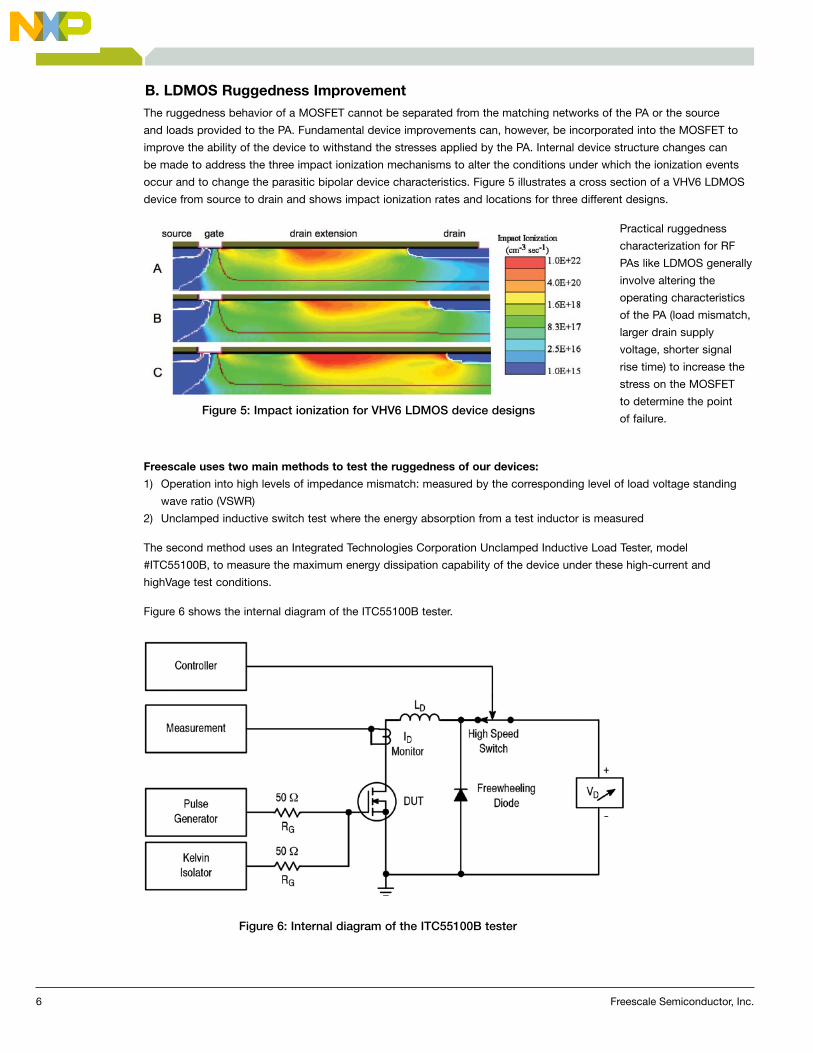
B. LDMOS Ruggedness ImprovementThe ruggedness behavior of a MOSFET cannot be separated from the matching networks of the PA or the source
and loads provided to the PA. Fundamental device improvements can, however, be incorporated into the MOSFET to
improve the ability of the device to withstand the stresses applied by the PA. Internal device structure changes can
be made to address the three impact ionization mechanisms to alter the conditions under which the ionization events
occur and to change the parasitic bipolar device characteristics. Figure 5 illustrates a cross section of a VHV6 LDMOS
device from source to drain and shows impact ionization rates and locations for three different designs.
Practical ruggedness
characterization for RF
PAs like LDMOS generally
involve altering the
operating characteristics
of the PA (load mismatch,
larger drain supply
voltage, shorter signal
rise time) to increase the
stress on the MOSFET
to determine the point
of failure.
Freescale uses two main methods to test the ruggedness of our devices:
1) Operation into high levels of impedance mismatch: measured by the corresponding level of load voltage standing
wave ratio (VSWR)
2) Unclamped inductive switch test where the energy absorption from a test inductor is measured
The second method uses an Integrated Technologies Corporation Unclamped Inductive Load Tester, model
#ITC55100B, to measure the maximum energy dissipation capability of the device under these high-current and
highVage test conditions.
Figure 6 shows the internal diagram of the ITC55100B tester.
Figure 5: Impact ionization for VHV6 LDMOS device designs
Figure 6: Internal diagram of the ITC55100B tester

Freescale Semiconductor, Inc. 7
The tester controller activates the pulse generator to turn on the device under test (DUT) through the limiting and terminating
resistor, RG, creating a very clean gate pulse waveform. This pulse waveform tests the maximum energy dissipation
capability of the DUT by stressing it under various controlled energy levels. This is accomplished by attaching an unclamped
inductive load to the device’s drain and source connection and then increasing both the load current and load voltage
up until the point that the DUT failure is achieved. This test method for power devices gives repeatable, quantitative and
reliable data needed to evaluate an LDMOS transistor’s ability to survive stresses that could cause an avalanche mode
failure. The final maximum energy dissipation capability rating, in joules, is calculated by the following equation:
where L is the load inductance value and I is the peak current within the load inductor.
Figure 7 shows how internal device engineering has had a major positive influence on the ruggedness of the devices in
these tests.
Parameter 1 kW Non-Rugged 1 kW Rugged Improvement Factor
Max Voltage 164V 195V +18%
IDpeak 40A 80A +100%
Energy Absorbed 1.53J 5.30J +240%
Table 2: Impact of ruggedness design changes
Freescale developed the EVHV6 50V LDMOS process for industrial applications such as plasma generators, CO2 lasers
and MRIs, where withstanding extremely high VSWRs is a requirement. This EVHV6 process enhancement to the VHV6
technology creates devices that can withstand VSWRs greater than 65:1 at all phase angles at their rated power.
Freescale has developed a process where improved ruggedness does not compromise RF performance, making
Freescale E series devices suitable for any application where ruggedness would be a benefit.
1.25 kW device absorbs 5.30 joules and survives Non-rugged 1 kW devices fail after absorbing 1.53 joules
Figure 7: Voltage and current curves during energy discharge
8 Freescale Semiconductor, Inc.
IV. DESIGN FEATURESThis section will cover the design features for the 50V RF power devices. RF performance, thermal characteristics,
device impedances and device models will be included.
A. 50V Ruggedized Devices Freescale now offers four new ultra-rugged 50V power devices designed for ISM applications. These 50V devices cover
power levels from 300W to 1.25 kW and frequencies from 1.8 MHz to 860 MHz. Subscribe to Freescale’s
Design News newsletter to receive information on new product releases.(9)
Product Power Level Frequency Range Package Style Package Type
MRFE6VP61K25H 1250W 1.8–600 MHz Push-Pull Air Cavity Ceramic
MRFE6VP5600H 600W 1.8–600 MHz Push-Pull Air Cavity Ceramic
MRFE6VP8600H 600W125W Avg. (DVB-T) 470–860 MHz Push-Pull Air Cavity Ceramic
MRFE6VP6300H 300W 1.8–600 MHz Push-Pull Air Cavity Ceramic
Table 3: Freescale ruggedized 50V product offerings
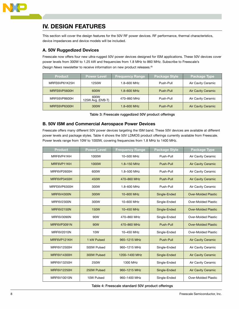
B. 50V ISM and Commercial Aerospace Power Devices Freescale offers many different 50V power devices targeting the ISM band. These 50V devices are available at different
power levels and package styles. Table 4 shows the 50V LDMOS product offerings currently available from Freescale.
Power levels range from 10W to 1000W, covering frequencies from 1.8 MHz to 1400 MHz.
Product Power Level Frequency Range Package Style Package Type
MRF6VP41KH 1000W 10–500 MHz Push-Pull Air Cavity Ceramic
MRF6VP11KH 1000W 1.8–150 MHz Push-Pull Air Cavity Ceramic
MRF6VP2600H 600W 1.8–500 MHz Push-Pull Air Cavity Ceramic
MRF6VP3450H 450W 470–860 MHz Push-Pull Air Cavity Ceramic
MRFE6VP6300H 300W 1.8–600 MHz Push-Pull Air Cavity Ceramic
MRF6V4300N 300W 10–600 MHz Single-Ended Over-Molded Plastic
MRF6V2300N 300W 10–600 MHz Single-Ended Over-Molded Plastic
MRF6V2150N 150W 10–450 MHz Single-Ended Over-Molded Plastic
MRF6V3090N 90W 470–860 MHz Single-Ended Over-Molded Plastic
MRF6VP3091N 90W 470–860 MHz Push-Pull Over-Molded Plastic
MRF6V2010N 10W 10–450 MHz Single-Ended Over-Molded Plastic
MRF6VP121KH 1 kW Pulsed 965–1215 MHz Push-Pull Air Cavity Ceramic
MRF6V12500H 500W Pulsed 960–1215 MHz Single-Ended Air Cavity Ceramic
MRF6V14300H 300W Pulsed 1200–1400 MHz Single-Ended Air Cavity Ceramic
MRF6V13250H 250W 1300 MHz Single-Ended Air Cavity Ceramic
MRF6V12250H 250W Pulsed 960–1215 MHz Single-Ended Air Cavity Ceramic
MRF6V10010N 10W Pulsed 960–1400 MHz Single-Ended Over-Molded Plastic
Table 4: Freescale standard 50V product offerings

Freescale Semiconductor, Inc. 9
C. Examples of 50V Power DevicesThe MRFE6VP61K25H is a versatile device and is well suited for a wide range of applications. It is capable of delivering
over 1 kW CW and will withstand extreme mismatches, even at rated output power. This is due to its high efficiency,
low thermal resistance and ruggedized silicon design.
An excellent example of an application of this device can be seen in the reference circuit for the 87.5–108 MHz FM broadcast
band. Over this frequency range, the device has output power greater than 1100W, gain greater than 24 dB and drain
efficiency greater than 80%. Performance was characterized using the 87.5–108 MHz application circuit as shown in Figure 8.
Figure 9 shows the broadband performance for the 87.5–108 MHz application circuit.
As another example, the MRF6V12500HS has been designed to cover the 960 to 1215 MHz frequency range. Figure 10
shows the compact broadband circuit board layout of only 3.2 x 2.2 inches.
Typical performance for this 960 to 1215 MHz pulsed design is shown in Figure 11. In this test circuit with 500W output,
the gain is more than 17.5 dB with better than 1 dB gain flatness and drain efficiency is greater than 56%.
Figure 9: CW performance graph with low pass filter versus output power
Figure 10: MRF6V12500HS broadband fixture
Figure 8: 87.5–108 MHz FM broadcast application circuit
Figure 11: MRF6V12500HS RF performance curves circuit performance

10 Freescale Semiconductor, Inc.
D. 50V LDMOS Thermal Performance Freescale 50V LDMOS devices have been designed for both excellent RF and thermal performance in intended
applications. The devices are optimized thermally for both pulse and CW applications.
Figure 12 shows a plot of transient thermal impedance for the MRFE6VP61K25H device under various pulse conditions.
The bottom axis shows pulse width in seconds and curves for two different duty cycles. As an example, a pulse width of
100 µsec and a duty cycle of 10% shows a θjc of 0.22°C/W. From this graph the CW θjc can be seen to be 0.15°C/W.
Figure 13 shows the MTTF versus junction temperature for CW conditions. This graph assumes a power output of
1250W CW, a drain voltage of 50 Vdc and a drain efficiency over 74%. As an example, the graph shows that at a
150ºC junction temperature, the MTTF is approximately 4.5 million hours, or 513 years.
Figure 13: MTTF versus junction temperature for MRFE6VP61K25H
Figure 12: MRFE6VP61K25H transient thermal impedance
°
TO-270 WB-4TO-270 WB-4
NI-780S-2NI-780S-2 NI-780S-4
NI-1230-4

Freescale Semiconductor, Inc. 11
Figure 14: MRF6V3090N RF performance curves, simulated versus measured Pulse width = 128 µsec, duty cycle = 10%
E. 50V LDMOS Device ModelsModels are available to assist customers simulating designs using Freescale 50V LDMOS devices. Table 5 shows the
status of models for currently available devices.
As an example of the benefits of using Freescale 50V LDMOS product models, Figure 14 shows the RF performance
curves for the MRF6V3090N with both measured data in a broadband test fixture and product model simulations
for a 960 to 1215 MHz L-band pulsed application. Table 6 shows a comparison of the measured versus simulated
performance results under pulsed conditions.
Product Agilent ADS
AWR Microwave Office®
MRFE6VP61K25H Now Now
MRFE6VP5600H Now Now
MRFE6VP6300H Now Now
MRFE6VP8600H 9/2011 9/2011
MRF6V2010N Now Now
MRF6V2150N Now Now
MRF6V2300N Now Now
MRF6V4300N Now Now
MRF6VP2600H Now Now
MRF6VP11KH Now Now
Product Agilent ADS
AWR Microwave Office
MRF6VP41KH Now Now
MRF6V14300H Now Now
MRF6V13250H Now Now
MRF6V10010N Now -
MRF6V12250H Now Now
MRF6V3090N Now Now
MRF6VP3091N 9/2011 9/2011
MRF6VP121KH - -
MRF6VP3450H Now Now
MRF6V12500H Now Now
Table 5: Freescale 50V product models
Simulated Measured
Frequency Power Level Power Gain Drain Efficiency Power Gain Drain Efficiency
960 MHz 90W 17.7 dB 47.7% 18.2 dB 55.1%
1090 MHz 90W 18.1 dB 54.3% 17.3 dB 51.2%
1215 MHz 90W 17.2 dB 44.4% 17.2 dB 51.7%
Table 6: MRF6V3090N RF performance, simulated versus measured Pulse width = 128 µsec, duty cycle = 10%
12 Freescale Semiconductor, Inc.
V. SUMMARYFreescale has successfully leveraged its position as the world’s leading supplier of high-power RF LDMOS transistors to
develop, qualify and release to manufacturing a portfolio of 50V LDMOS products specifically designed for the unique
requirements of the ISM, broadcast and commercial aerospace market segments. Compared to the existing competitors
and technologies used in these market segments, Freescale’s 50V LDMOS provides superior power, gain, linearity,
efficiency and ruggedness.
This paper has described the device technology along with key features, presented details on how extreme ruggedness
is achieved and outlined performance and design features of the portfolio. Freescale is committed to delivering
compelling solutions to the RF power market, including an aggressive development program to maintain Freescale’s
innovative leadership.
REFERENCES[1-8]
A. Wood et al., “High performance silicon LDMOS technology for 2 GHz RF power amplifier applications,”
1996 IEEE IEDM, pp. 87–90.
G. Ma et al., “High efficiency LDMOS power FET for low voltage wireless communications”,
1996 IEEE IEDM, pp. 91–94.
A. Wood, “120 Watt, 2 GHz, Si LDMOS RF power transistor for PCS base station applications,”
1998 IEEE IMS Symposium, pp. 707–710 vol.2.
H. Brech et al., “Record efficiency and gain at 2.1 GHz of high power RF transistors for cellular and 3G base stations,”
2003 IEEE IEDM, pp. 15.1.1–15.1.4.
C. Dragon et al., “200W push-pull & 110W single-ended high performance RF-LDMOS transistors for WCDMA
base station applications,” 2003 IEEE IMS Symposium, pp. 69–72 vol.1.
W. Burger et al., “RF-LDMOS: a device technology for high power RF infrastructure applications,”
2004 IEEE CSICS, pp. 189–192.
C. Cassan, P. Gola “A 3.5 GHz 25W Silicon LDMOS RFIC Power Amplifier for WiMax Applications,”
2007 IEEE RFIC Symposium, pp. 87–90.
X. Moronval, P. Peyrot “Industry First 100W Two-Stage RFIC for 900 MHz GSM/EDGE Base Station Applications,”
2007 IEEE IMS Symposium, pp. 1585–1588.
[9] Refer to freescale.com/newsletter to subscribe to the Freescale Design News newsletter to receive information on
RF power product updates.

Freescale and the Freescale logo are trademarks of Freescale Semiconductor, Inc., Reg. U.S. Pat. & Tm. Off. All other product or service names are the property of their respective owners. © 2010, 2011 Freescale Semiconductor, Inc.
Document Number: 50VRFLDMOSWP Rev. 4 9/2011
How to Reach Us:
Information in this document is provided solely to enable system and software implementers to use Freescale Semiconductor products. There are no express or implied copyright license granted hereunder to design or fabricate any integrated circuits or integrated circuits based on the information in this document.
Freescale Semiconductor reserves the right to make changes without further notice to any products herein. Freescale Semiconductor makes no warranty, representation or guarantee regarding the suitability of its products for any particular purpose, nor does Freescale Semiconductor assume any liability arising out of the application or use of any product or circuit, and specifically disclaims any and all liability, including without limitation consequential or incidental damages. “Typical” parameters which may be provided in Freescale Semiconductor data sheets and/or specifications can and do vary in different applications and actual performance may vary over time. All operating parameters, including “Typicals” must be validated for each customer application by customer’s technical experts. Freescale Semiconductor does not convey any license under its patent rights nor the rights of others. Freescale Semiconductor products are not designed, intended, or authorized for use as components in systems intended for surgical implant into the body, or other applications intended to support or sustain life, or for any other application in which the failure of the Freescale Semiconductor product could create a situation where personal injury or death may occur. Should Buyer purchase or use Freescale Semiconductor products for any such unintended or unauthorized application, Buyer shall indemnify and hold Freescale Semiconductor and its officers, employees, subsidiaries, affiliates, and distributors harmless against all claims, costs, damages, and expenses, and reasonable attorney fees arising out of, directly or indirectly, any claim of personal injury or death associated with such unintended or unauthorized use, even if such claim alleges that Freescale Semiconductor was negligent regarding the design or manufacture of the part.
Home Page:www.freescale.com
Web Support:www.freescale.com/support
USA/Europe or Locations Not Listed:Freescale Semiconductor, Inc.Technical Information Center, EL5162100 E. Elliot RoadTempe, Arizona 852841-800-521-6274 or +1-480-768-2130www.freescale.com/support
Europe, Middle East, and Africa:Freescale Halbleiter Deutschland GmbHTechnical Information CenterSchatzbogen 781829 Muenchen, Germany+44 1296 380 456 (English)+46 8 52200080 (English)+49 89 92103 559 (German)+33 1 69 35 48 48 (French)[email protected]
Japan:Freescale Semiconductor Japan Ltd.HeadquartersARCO Tower 15F1-8-1, Shimo-Meguro, Meguro-ku,Tokyo 153-0064, Japan0120 191014+81 3 5437 [email protected]
Asia/Pacific:Freescale Semiconductor China Ltd.Exchange Building 23FNo. 118 Jianguo RoadChaoyang DistrictBeijing 100022China +86 10 5879 8000 [email protected]
For Literature Requests Only:Freescale Semiconductor Literature Distribution Center1-800-441-2447 or +1-303-675-2140Fax: [email protected]
Recommended