An Interactive Workshop on
Field Programmable Gate Arrays (FPGAs)
21st – 23rd July 2009
Prepared by
Shahzad Asif Lecturer
MS (System on Chip) Linköping University
Sweden
Department of Electrical Engineering COMSATS Institute of Information Technology
Chak Shahzad Campus, Islamabad.
An Interactive WorkshopAn Interactive Workshoponon
Field Programmable Gate Array (FPGA)Field Programmable Gate Array (FPGA)
Speaker: Shahzad AsifSpeaker: Shahzad AsifLecturer (EE Department)Lecturer (EE Department)MS(SystemMS(System--onon--Chip)Chip)LinkLinkööping University, Sweden.ping University, Sweden.
22
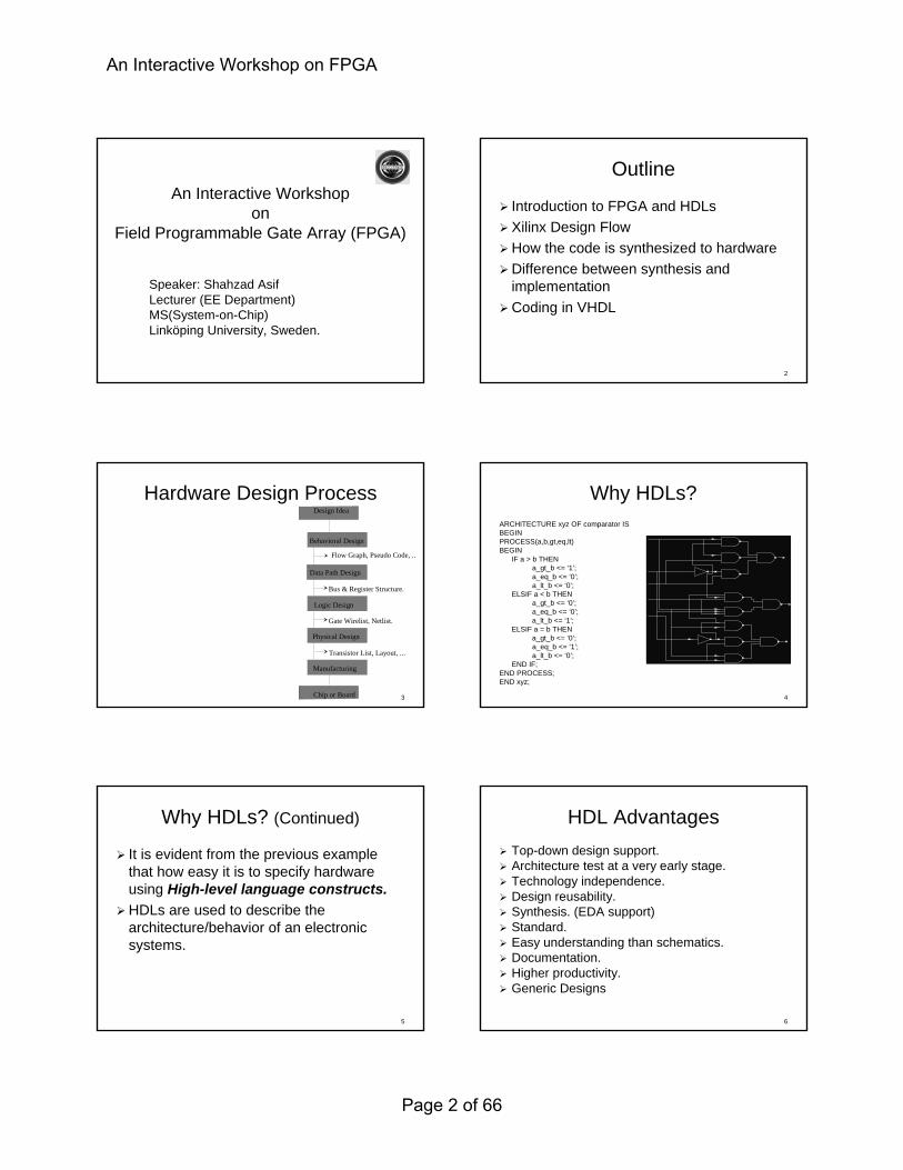
OutlineOutline
Introduction to FPGA and HDLsIntroduction to FPGA and HDLsXilinx Design FlowXilinx Design FlowHow the code is synthesized to hardwareHow the code is synthesized to hardwareDifference between synthesis and Difference between synthesis and implementationimplementationCoding in VHDLCoding in VHDL
33
Hardware Design ProcessHardware Design Process
Flow Graph, Pseudo Code, ..
Design Idea
Behavioral Design
Data Path Design
Logic Design
Physical Design
Manufacturing
Chip or Board
Bus & Register Structure.
Gate Wirelist, Netlist.
Transistor List, Layout, ...
44
Why HDLs?Why HDLs?ARCHITECTURE xyz OF comparator ISARCHITECTURE xyz OF comparator ISBEGINBEGINPROCESS(a,b,gt,eq,ltPROCESS(a,b,gt,eq,lt))BEGINBEGIN
IF a > b THENIF a > b THENa_gt_ba_gt_b <= <= ‘‘11’’;;a_eq_ba_eq_b <= <= ‘‘00’’;;a_lt_ba_lt_b <= <= ‘‘00’’;;
ELSIF a < b THENELSIF a < b THENa_gt_ba_gt_b <= <= ‘‘00’’;;a_eq_ba_eq_b <= <= ‘‘00’’;;a_lt_ba_lt_b <= <= ‘‘11’’;;
ELSIF a = b THENELSIF a = b THENa_gt_ba_gt_b <= <= ‘‘00’’;;a_eq_ba_eq_b <= <= ‘‘11’’;;a_lt_ba_lt_b <= <= ‘‘00’’;;
END IF;END IF;END PROCESS;END PROCESS;END xyz;END xyz;
1
23
1
23
1
23
1
23
128
9
128
9
1
23
128
9
1 2
1 2
1
23
128
9
1
23
a
b
gt
eq
lt
a_gt_b
a_eq_b
a_lt_b
55
Why HDLs? Why HDLs? (Continued)(Continued)
It is evident from the previous example that how easy it is to specify hardware using High-level language constructs.HDLs are used to describe the architecture/behavior of an electronic systems.
66
HDL AdvantagesHDL AdvantagesTopTop--down design support.down design support.Architecture test at a very early stage.Architecture test at a very early stage.Technology independence.Technology independence.Design reusability.Design reusability.Synthesis. (EDA support)Synthesis. (EDA support)Standard.Standard.Easy understanding than schematics.Easy understanding than schematics.Documentation.Documentation.Higher productivity.Higher productivity.Generic DesignsGeneric Designs
An Interactive Workshop on FPGA
Page 2 of 66
77
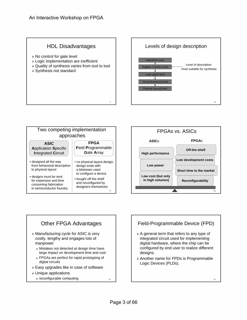
HDL DisadvantagesHDL Disadvantages
No control for gate levelNo control for gate levelLogic implementation are inefficientLogic implementation are inefficientQuality of synthesis varies from tool to toolQuality of synthesis varies from tool to toolSynthesis not standardSynthesis not standard
88
Levels of design descriptionLevels of design description
Algorithmic level
Register Transfer Level
Logic (gate) level
Circuit (transistor) level
Physical (layout) level
Level of description most suitable for synthesis
99
• designs must be sentfor expensive and timeconsuming fabricationin semiconductor foundry
• bought off the shelfand reconfigured bydesigners themselves
Two competing implementation Two competing implementation approachesapproaches
ASICApplication Specific
Integrated Circuit
FPGAField Programmable
Gate Array
• designed all the wayfrom behavioral descriptionto physical layout
• no physical layout design;design ends witha bitstream usedto configure a device
1010
FPGAsFPGAs vs. vs. ASICsASICs
ASICs FPGAs
High performanceOff-the-shelf
Short time to the market
Low development costs
Reconfigurability
Low power
Low cost (but only in high volumes)
1111
Other FPGA AdvantagesOther FPGA Advantages
Manufacturing cycle for ASIC is very Manufacturing cycle for ASIC is very costly, lengthy and engages lots of costly, lengthy and engages lots of manpowermanpower
Mistakes not detected at design time have Mistakes not detected at design time have large impact on development time and costlarge impact on development time and costFPGAs are perfect for rapid prototyping of FPGAs are perfect for rapid prototyping of digital circuitsdigital circuits
Easy upgrades like in case of softwareEasy upgrades like in case of softwareUnique applicationsUnique applications
reconfigurable computingreconfigurable computing 1212
FieldField--Programmable Device (FPD)Programmable Device (FPD)
A general term that refers to any type of A general term that refers to any type of integrated circuit used for implementing integrated circuit used for implementing digital hardware, where the chip can be digital hardware, where the chip can be configured by end user to realize different configured by end user to realize different designs.designs.Another name for FPDs is Programmable Another name for FPDs is Programmable Logic Devices (PLDs).Logic Devices (PLDs).
An Interactive Workshop on FPGA
Page 3 of 66

1313
Types of FPDTypes of FPDProgrammable Logic Array (PLA)Programmable Logic Array (PLA)
Contains two levels of logic, an ANDContains two levels of logic, an AND--plane and an ORplane and an OR--plane.plane.Programmable Array Logic (PAL)Programmable Array Logic (PAL)
Programmable ANDProgrammable AND--plane, fixed ORplane, fixed OR--planeplaneSimple PLD (SPLD)Simple PLD (SPLD)
usually refers to PLA or PAL.usually refers to PLA or PAL.Complex PLD (CPLD)Complex PLD (CPLD)
Consists of an arrangement of multiple SPLDConsists of an arrangement of multiple SPLD--like blocks on a like blocks on a single chip.single chip.
FieldField--Programmable Gate ArrayProgrammable Gate ArrayWhereas CPLDs feature logic resources with a wide number of Whereas CPLDs feature logic resources with a wide number of inputs (AND planes), FPGAs offer more narrow logic resources.inputs (AND planes), FPGAs offer more narrow logic resources.Offer a higher ratio of flipOffer a higher ratio of flip--flops to logic resources compared to flops to logic resources compared to CPLDs.CPLDs.
1414
FPGAFPGA
Block R
AM
s
Block R
AM
s
ConfigurableLogicBlocks
I/OBlocks
BlockRAMs
1515
FPGAFPGA
Building block of an FPGA is a CLB Building block of an FPGA is a CLB (Configurable Logic Block).(Configurable Logic Block).A typical CLB consist of 4A typical CLB consist of 4--input LUT(Look input LUT(Look Up Table), D flipUp Table), D flip--flop, and two input flop, and two input multiplexer.multiplexer.
1616
Major FPGA VendorsMajor FPGA VendorsXilinx, Inc.Xilinx, Inc.AlteraAltera Corp.Corp.AtmelAtmelLattice SemiconductorLattice Semiconductor
Xilinx
All Others
FPGA Vendors
Altera
58%
31% 11%
1717
FPGA NomenclatureFPGA Nomenclature
XC3S1500-4FG320
Spartan 3family
1500 k= 1.5 M
equivalent logic gates
speed grade
-4= standard
performance
320 pins
package type
1818
Design Implementation in LUTDesign Implementation in LUT
001111111010110101110000
DataDataAddressAddress2-input Lookup Table
2-input NAND Gate
111111001010000101000000
DataDataAddressAddress2-input Lookup Table
2-input AND Gate
An Interactive Workshop on FPGA
Page 4 of 66
1919
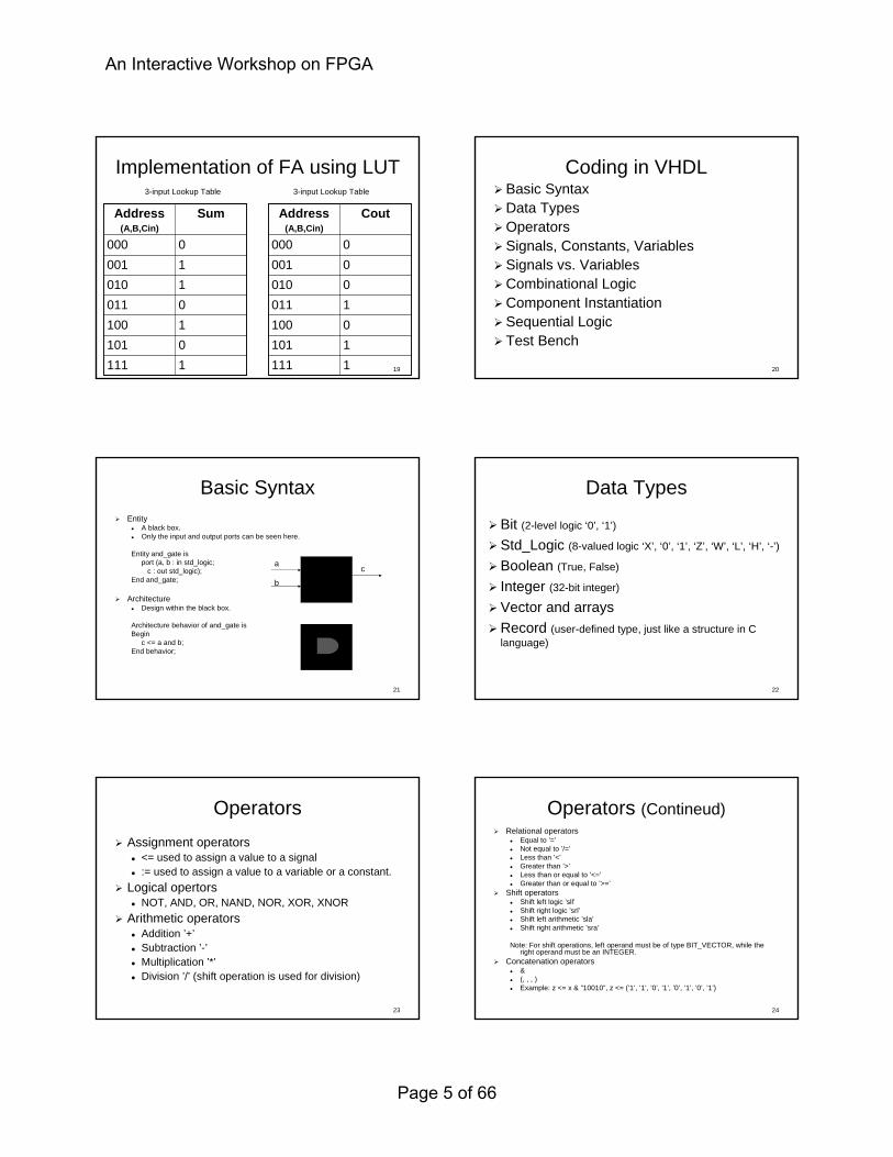
Implementation of FA using LUTImplementation of FA using LUT
11111111001011011110010000011011110100101100100100000000
SumSumAddressAddress(A,B,Cin)(A,B,Cin)
3-input Lookup Table
11111111111011010010010011011011000100100000100100000000
CoutCoutAddressAddress(A,B,Cin)(A,B,Cin)
3-input Lookup Table
2020
Coding in VHDLCoding in VHDLBasic SyntaxBasic SyntaxData TypesData TypesOperatorsOperatorsSignals, Constants, VariablesSignals, Constants, VariablesSignals vs. VariablesSignals vs. VariablesCombinational LogicCombinational LogicComponent InstantiationComponent InstantiationSequential LogicSequential LogicTest BenchTest Bench
2121
Basic SyntaxBasic SyntaxEntityEntity
A black box.A black box.Only the input and output ports can be seen here.Only the input and output ports can be seen here.
Entity and_gate isEntity and_gate isport (a, b : in std_logic;port (a, b : in std_logic;
c : out std_logic);c : out std_logic);End and_gate;End and_gate;
ArchitectureArchitectureDesign within the black box.Design within the black box.
Architecture behavior of and_gate isArchitecture behavior of and_gate isBeginBegin
c <= a and b;c <= a and b;End behavior;End behavior;
a
b
c
2222
Data TypesData Types
Bit Bit (2(2--level logic level logic ‘‘00’’, , ‘‘11’’))
Std_Logic Std_Logic (8(8--valued logic valued logic ‘‘XX’’, , ‘‘00’’, , ‘‘11’’, , ‘‘ZZ’’, , ‘‘WW’’, , ‘‘LL’’, , ‘‘HH’’, , ‘‘--’’))
Boolean Boolean (True, False)(True, False)
Integer Integer (32(32--bit integer)bit integer)
Vector and arraysVector and arraysRecord Record (user(user--defined type, just like a structure in C defined type, just like a structure in C language)language)
2323
OperatorsOperatorsAssignment operatorsAssignment operators
<= used to assign a value to a signal<= used to assign a value to a signal:= used to assign a value to a variable or a constant.:= used to assign a value to a variable or a constant.
Logical opertorsLogical opertorsNOT, AND, OR, NAND, NOR, XOR, XNORNOT, AND, OR, NAND, NOR, XOR, XNOR
Arithmetic operatorsArithmetic operatorsAddition Addition ’’++’’Subtraction Subtraction ’’--’’Multiplication Multiplication ’’**’’Division Division ’’//’’ (shift operation is used for division)(shift operation is used for division)
2424
Operators Operators (Contineud)(Contineud)Relational operatorsRelational operators
Equal to Equal to ’’==’’Not equal to Not equal to ’’/=/=’’Less than Less than ’’<<’’Greater than Greater than ’’>>’’Less than or equal to Less than or equal to ’’<=<=’’Greater than or equal to Greater than or equal to ’’>=>=’’
Shift operatorsShift operatorsShift left logic Shift left logic ’’sllsll’’Shift right logic Shift right logic ’’srlsrl’’Shift left arithmetic Shift left arithmetic ’’slasla’’Shift right arithmetic Shift right arithmetic ’’srasra’’
Note: For shift operations, left operand must be of type BIT_VECNote: For shift operations, left operand must be of type BIT_VECTOR, while the TOR, while the right operand must be an INTEGER.right operand must be an INTEGER.
Concatenation operatorsConcatenation operators&&(, , , )(, , , )Example: z <= x & Example: z <= x & ””1001010010””, z <= (, z <= (’’11’’, , ’’11’’, , ’’00’’, , ’’11’’, , ’’00’’, , ’’11’’, , ’’00’’, , ’’11’’))
An Interactive Workshop on FPGA
Page 5 of 66
2525
Signals, Constants, VariablesSignals, Constants, VariablesCONSTANTCONSTANT
A CONSTANT can be declared in a PACKAGE, ENTITY, or ARCHITECTUREA CONSTANT can be declared in a PACKAGE, ENTITY, or ARCHITECTURE..
•• CONSTANT set_bit : BIT := CONSTANT set_bit : BIT := ‘‘11’’;;SIGNALSIGNAL
SIGNAL represents circuit interconnects (wires).SIGNAL represents circuit interconnects (wires).SIGNAL can be declared in a PACKAGE, ENTITY, or ARCHITECTURE.SIGNAL can be declared in a PACKAGE, ENTITY, or ARCHITECTURE.Its update is not immediate. In other words, its new value is noIts update is not immediate. In other words, its new value is not available until the t available until the conclusion of the corresponding PROCESS, FUNCTION, or PROCEDURE.conclusion of the corresponding PROCESS, FUNCTION, or PROCEDURE.
•• SIGNAL y : SIGNAL y : std_logic_vectorstd_logic_vector (7 (7 downtodownto 0);0);•• SIGNAL control : SIGNAL control : std_logicstd_logic := := ‘‘11’’;;
Note: Initial value in the syntax above is not synthesizable.Note: Initial value in the syntax above is not synthesizable.VARIABLEVARIABLE
It can only be used inside a PROCESS FUNCTION, or PROCEDURE.It can only be used inside a PROCESS FUNCTION, or PROCEDURE.Unlike SIGNAL, its update is immediate, so the new value can be Unlike SIGNAL, its update is immediate, so the new value can be promptly used promptly used in the next line of code.in the next line of code.
•• VARIABLE y : VARIABLE y : std_logic_vectorstd_logic_vector (7 (7 downtodownto 0) := 0) := ““1000100010001000””;;
2626
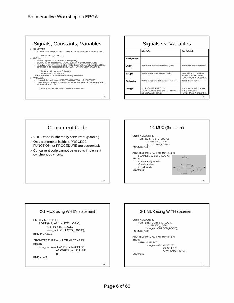
Signals vs. VariablesSignals vs. Variables
Only in sequential code, that Only in sequential code, that is, in a PROCESS, is, in a PROCESS, FUNCTION, or PROCEDURE.FUNCTION, or PROCEDURE.
In a PACKAGE, ENTITY, or In a PACKAGE, ENTITY, or ARCHITECTURE. In an ENTITY, all PORTS ARCHITECTURE. In an ENTITY, all PORTS are SIGNALS by default.are SIGNALS by default.
UsageUsage
Updated immediatelyUpdated immediatelyUpdate is not immediate in sequential codeUpdate is not immediate in sequential codeBehaviorBehavior
Local (visible only inside the Local (visible only inside the corresponding PROCESS, corresponding PROCESS, FUNCTION, or PROCEDURE)FUNCTION, or PROCEDURE)
Can be global (seen by entire code)Can be global (seen by entire code)ScopeScope
Represents local informationRepresents local informationRepresents circuit interconnects (wires)Represents circuit interconnects (wires)UtilityUtility
:=:=<=<=AssignmentAssignment
VARIABLEVARIABLESIGNALSIGNAL
2727
Concurrent CodeConcurrent Code
VHDL code is inherently concurrent (parallel)VHDL code is inherently concurrent (parallel)Only statements inside a PROCESS, Only statements inside a PROCESS, FUNCTION, or PROCEDURE are sequential.FUNCTION, or PROCEDURE are sequential.Concurrent code cannot be used to implement Concurrent code cannot be used to implement synchronous circuits.synchronous circuits.
2828
ENTITY MUX2to1 ISENTITY MUX2to1 ISPORT (a, b : IN STD_LOGIC;PORT (a, b : IN STD_LOGIC;
selsel : IN STD_LOGIC;: IN STD_LOGIC;q : OUT STD_LOGIC);q : OUT STD_LOGIC);
END MUX2to1;END MUX2to1;
ARCHITECTURE mux1 OF MUX2to1 ISARCHITECTURE mux1 OF MUX2to1 ISSIGNAL s1, s2 : STD_LOGIC;SIGNAL s1, s2 : STD_LOGIC;
BEGINBEGINa1 a1 <= a and (not <= a and (not selsel););a2 <= b and a2 <= b and selsel;;q<= a1 or a2;q<= a1 or a2;
END mux1;END mux1;
22--1 MUX (Structural)1 MUX (Structural)
2929
22--1 MUX using WHEN statement1 MUX using WHEN statement
ENTITY MUX2to1 ISENTITY MUX2to1 ISPORT (in1, in2 : IN STD_LOGIC;PORT (in1, in2 : IN STD_LOGIC;
selsel : IN STD_LOGIC;: IN STD_LOGIC;mux_outmux_out : OUT STD_LOGIC);: OUT STD_LOGIC);
END MUX2to1;END MUX2to1;
ARCHITECTURE mux2 OF MUX2to1 ISARCHITECTURE mux2 OF MUX2to1 ISBEGINBEGIN
mux_outmux_out <= in1 WHEN <= in1 WHEN selsel==‘‘00’’ ELSEELSEin2 WHEN in2 WHEN selsel==‘‘11’’ ELSEELSE‘‘00’’;;
END mux2;END mux2;
3030
22--1 MUX using WITH statement1 MUX using WITH statement
ENTITY MUX2to1 ISENTITY MUX2to1 ISPORT (in1, in2 : IN STD_LOGIC;PORT (in1, in2 : IN STD_LOGIC;
selsel : IN STD_LOGIC;: IN STD_LOGIC;mux_outmux_out : OUT STD_LOGIC);: OUT STD_LOGIC);
END MUX2to1;END MUX2to1;
ARCHITECTURE mux3 OF MUX2to1 ISARCHITECTURE mux3 OF MUX2to1 ISBEGINBEGIN
WITH WITH selsel SELECTSELECTmux_outmux_out <= in1 WHEN <= in1 WHEN ‘‘00’’,,
in2 WHEN in2 WHEN ‘‘11’’,,‘‘00’’ WHEN OTHERS;WHEN OTHERS;
END mux3;END mux3;
An Interactive Workshop on FPGA
Page 6 of 66
3131
TriTri--state Bufferstate Buffer
ENTITY ENTITY tri_statetri_state ISISPORT (PORT (enaena : IN STD_LOGIC;: IN STD_LOGIC;
input : IN STD_LOGIC_VECTOR(7 DOWNTO 0);input : IN STD_LOGIC_VECTOR(7 DOWNTO 0);output : OUT STD_LOGIC_VECTOR (7 DOWNTO 0) );output : OUT STD_LOGIC_VECTOR (7 DOWNTO 0) );
END END tri_statetri_state;;
ARCHITECTURE ARCHITECTURE arch_tri_statearch_tri_state OF OF tri_statetri_state ISISBEGINBEGIN
output <= input WHEN (output <= input WHEN (enaena==‘‘00’’) ELSE) ELSE(OTHERS => (OTHERS => ‘‘ZZ’’););
END END arch_tri_statearch_tri_state;;
3232
Half Adder (Structural)Half Adder (Structural)
ENTITY ENTITY half_adderhalf_adder ISISPORT (a, b : IN STD_LOGIC;PORT (a, b : IN STD_LOGIC;
sum, sum, coutcout : OUT STD_LOGIC);: OUT STD_LOGIC);END END half_adderhalf_adder;;
ARCHITECTURE ARCHITECTURE arch_half_adderarch_half_adder OF OF half_adderhalf_adder ISISBEGINBEGIN
sum <= a XOR b;sum <= a XOR b;coutcout <= a AND b;<= a AND b;
END END arch_half_adderarch_half_adder;;
3333
ComponentsComponentsAllows the construction of hierarchical designs.Allows the construction of hierarchical designs.Used for partitioning a code, code sharing, and code Used for partitioning a code, code sharing, and code reuse.reuse.To use (instantiate) a COMPONENT, it must first be To use (instantiate) a COMPONENT, it must first be declared.declared.
COMPONENT component_nameCOMPONENT component_namePORT (port_name : signal_mode signal_type;PORT (port_name : signal_mode signal_type;
port_name : signal_mode signal_type;port_name : signal_mode signal_type;...);...);
END COMPONENT;END COMPONENT;
3434
Components Components (Continued)(Continued)PORT MAPPORT MAP
Positional mapping (also called inPositional mapping (also called in--order mapping)order mapping)
COMPONENT inverterCOMPONENT inverterPORT (a : IN STD_LOGIC; PORT (a : IN STD_LOGIC;
b : OUT STD_LOGIC);b : OUT STD_LOGIC);END COMPONENT;END COMPONENT;
... ... ---- other codeother code
U1: inverter PORT MAP (x, y);U1: inverter PORT MAP (x, y);
3535
Components Components (Continued)(Continued)PORT MAPPORT MAP
Nominal mapping (also called outNominal mapping (also called out--ofof--order mapping)order mapping)Ports can also be left unconnected by using the keyword Ports can also be left unconnected by using the keyword ’’OPENOPEN’’. . Note that you should never leave the input port unconnected.Note that you should never leave the input port unconnected.
COMPONENT inverterCOMPONENT inverterPORT (a : IN STD_LOGIC; PORT (a : IN STD_LOGIC;
b : OUT STD_LOGIC;b : OUT STD_LOGIC;c : OUT STD_LOGIC);c : OUT STD_LOGIC);
END COMPONENT;END COMPONENT;
... ... ---- other codeother code
U1: inverter PORT MAP (aU1: inverter PORT MAP (a=>x=>x, b=>y, c=>OPEN);, b=>y, c=>OPEN);
3636
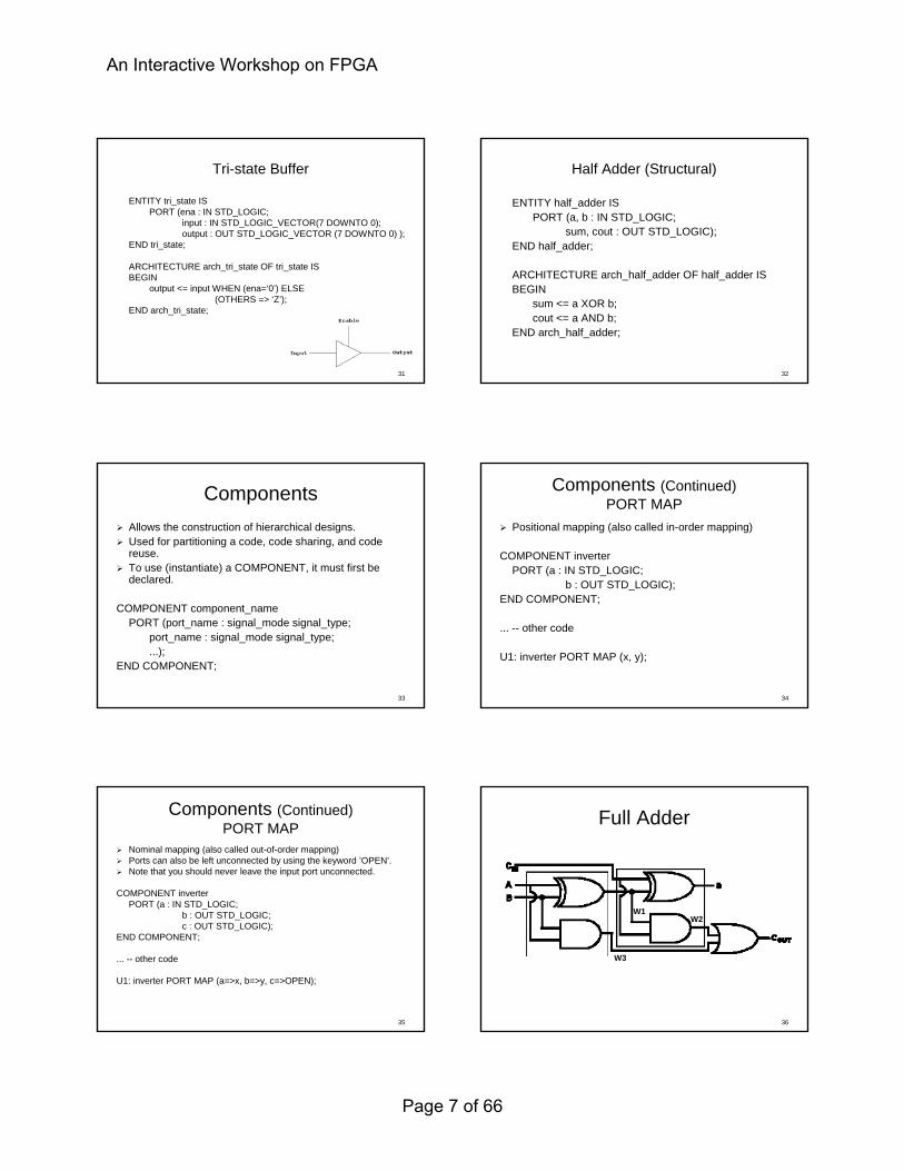
Full AdderFull Adder
W1
W3
W2
An Interactive Workshop on FPGA
Page 7 of 66
3737
Full Adder (Structural) Full Adder (Structural) (using component instantiation)(using component instantiation)
ENTITY ENTITY full_adderfull_adder ISISPORT (a, b, PORT (a, b, cincin : IN STD_LOGIC;: IN STD_LOGIC;
sum, sum, coutcout : OUT STD_LOGIC);: OUT STD_LOGIC);END END full_adderfull_adder;;
ARCHITECTURE ARCHITECTURE arch_full_adderarch_full_adder OF OF full_adderfull_adder ISISCOMPONENT COMPONENT half_adderhalf_adder
PORT ( a, b : IN STD_LOGIC;PORT ( a, b : IN STD_LOGIC;sum, sum, coutcout : OUT STD_LOGIC);: OUT STD_LOGIC);
END COMPONENT;END COMPONENT;BEGINBEGIN
C1: C1: half_adderhalf_adder PORT MAP(a,b,w1,w3);PORT MAP(a,b,w1,w3);C2: C2: half_adderhalf_adder PORT MAP(w1,cin,sum,w2);PORT MAP(w1,cin,sum,w2);coutcout <= w2 or w3;<= w2 or w3;
END END arch_full_adderarch_full_adder;;W1
W3
W2
3838
Test BenchTest Bench
Testing of a design is essential before Testing of a design is essential before physical fabrication.physical fabrication.We can write a VHDL program that We can write a VHDL program that encapsulates the DUT (Design Under encapsulates the DUT (Design Under Test), generates stimulus signals and Test), generates stimulus signals and captures the response signals. Such an captures the response signals. Such an arrangement is called a Test bench.arrangement is called a Test bench.
3939
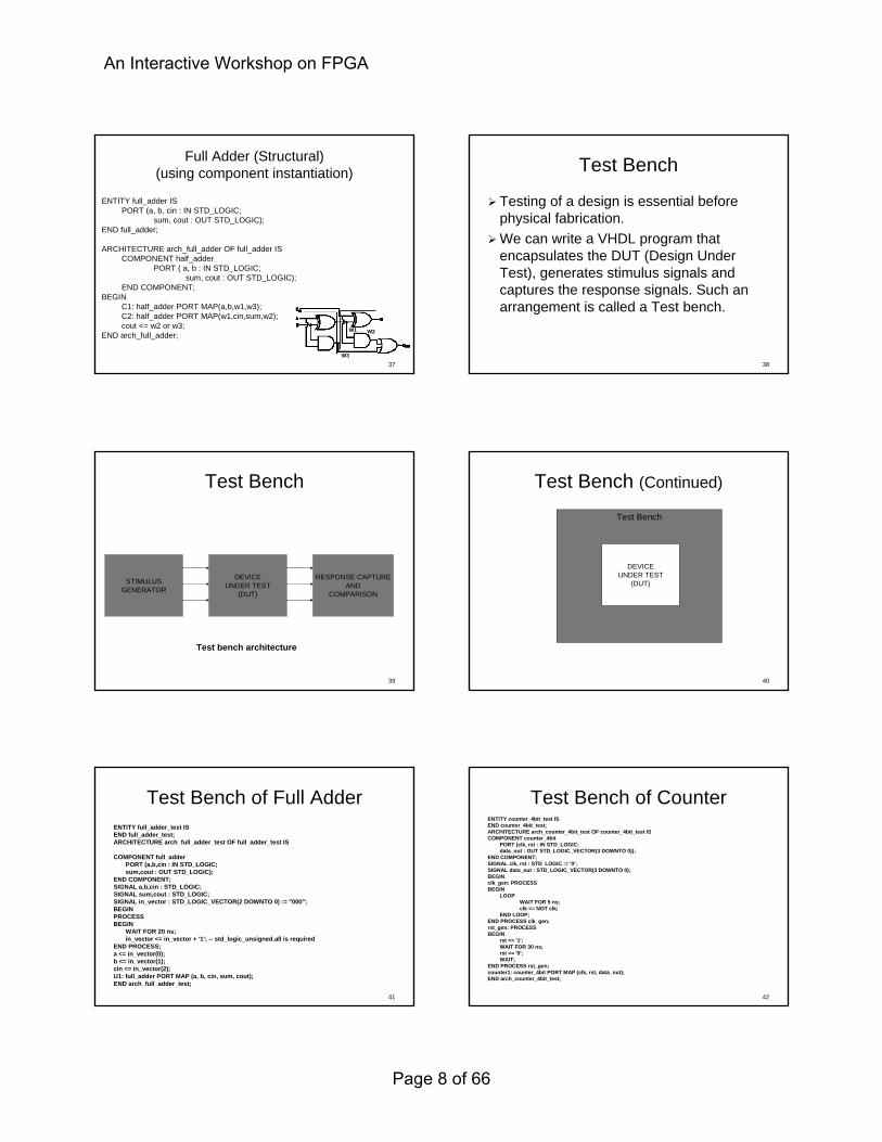
Test BenchTest Bench
DEVICEUNDER TEST
(DUT)
RESPONSE CAPTUREAND
COMPARISON
STIMULUSGENERATOR
Test bench architecture
4040
Test Bench
Test Bench Test Bench (Continued)(Continued)
DEVICEUNDER TEST
(DUT)
4141
Test Bench of Full AdderTest Bench of Full AdderENTITY ENTITY full_adder_testfull_adder_test ISISEND END full_adder_testfull_adder_test;;ARCHITECTURE ARCHITECTURE arch_full_adder_testarch_full_adder_test OF OF full_adder_testfull_adder_test ISIS
COMPONENT COMPONENT full_adderfull_adderPORT (PORT (a,b,cina,b,cin : IN STD_LOGIC;: IN STD_LOGIC;sum,coutsum,cout : OUT STD_LOGIC);: OUT STD_LOGIC);
END COMPONENT;END COMPONENT;SIGNAL SIGNAL a,b,cina,b,cin : STD_LOGIC;: STD_LOGIC;SIGNAL SIGNAL sum,coutsum,cout : STD_LOGIC; : STD_LOGIC; SIGNAL SIGNAL in_vectorin_vector : STD_LOGIC_VECTOR(2 DOWNTO 0) := "000";: STD_LOGIC_VECTOR(2 DOWNTO 0) := "000";BEGINBEGINPROCESSPROCESSBEGINBEGIN
WAIT FOR 20 ns;WAIT FOR 20 ns;in_vectorin_vector <= <= in_vectorin_vector + '1'; + '1'; ---- std_logic_unsigned.allstd_logic_unsigned.all is requiredis required
END PROCESS;END PROCESS;a <= in_vector(0);a <= in_vector(0);b <= in_vector(1);b <= in_vector(1);cincin <= in_vector(2);<= in_vector(2);U1: U1: full_adderfull_adder PORT MAP (a, b, PORT MAP (a, b, cincin, sum, , sum, coutcout););END END arch_full_adder_testarch_full_adder_test;;
4242
Test Bench of CounterTest Bench of CounterENTITY counter_4bit_test ISENTITY counter_4bit_test ISEND counter_4bit_test;END counter_4bit_test;ARCHITECTURE arch_counter_4bit_test OF counter_4bit_test ISARCHITECTURE arch_counter_4bit_test OF counter_4bit_test ISCOMPONENT counter_4bitCOMPONENT counter_4bit
PORT (PORT (clkclk, , rstrst : IN STD_LOGIC;: IN STD_LOGIC;data_outdata_out : OUT STD_LOGIC_VECTOR(3 DOWNTO 0));: OUT STD_LOGIC_VECTOR(3 DOWNTO 0));
END COMPONENT;END COMPONENT;SIGNAL SIGNAL clkclk, , rstrst : STD_LOGIC := '0';: STD_LOGIC := '0';SIGNAL SIGNAL data_outdata_out : STD_LOGIC_VECTOR(3 DOWNTO 0);: STD_LOGIC_VECTOR(3 DOWNTO 0);BEGINBEGINclk_genclk_gen: PROCESS: PROCESSBEGINBEGIN
LOOPLOOPWAIT FOR 5 ns;WAIT FOR 5 ns;clkclk <= NOT <= NOT clkclk;;
END LOOP;END LOOP;END PROCESS END PROCESS clk_genclk_gen;;rst_genrst_gen: PROCESS: PROCESSBEGINBEGIN
rstrst <= '1';<= '1';WAIT FOR 30 ns;WAIT FOR 30 ns;rstrst <= '0';<= '0';WAIT;WAIT;
END PROCESS END PROCESS rst_genrst_gen;;counter1: counter_4bit PORT MAP (counter1: counter_4bit PORT MAP (clkclk, , rstrst, , data_outdata_out););END arch_counter_4bit_test;END arch_counter_4bit_test;
An Interactive Workshop on FPGA
Page 8 of 66
4343
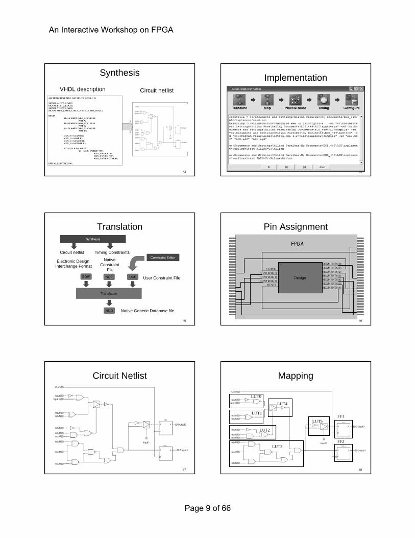
ARCHITECTURE MLU_DATAFLOW OF MLU IS
SIGNAL A1:STD_LOGIC;SIGNAL B1:STD_LOGIC;SIGNAL Y1:STD_LOGIC;SIGNAL MUX_0, MUX_1, MUX_2, MUX_3: STD_LOGIC;
BEGINA1<=A WHEN (NEG_A='0') ELSE
NOT A;B1<=B WHEN (NEG_B='0') ELSE
NOT B;Y<=Y1 WHEN (NEG_Y='0') ELSE
NOT Y1;
MUX_0<=A1 AND B1;MUX_1<=A1 OR B1;MUX_2<=A1 XOR B1;MUX_3<=A1 XNOR B1;
WITH (L1 & L0) SELECTY1<=MUX_0 WHEN "00",
MUX_1 WHEN "01",MUX_2 WHEN "10",MUX_3 WHEN OTHERS;
END MLU_DATAFLOW;
VHDL description Circuit netlist
SynthesisSynthesis
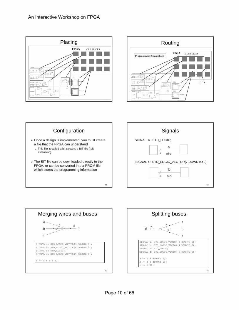
4444
ImplementationImplementation
4545
TranslationTranslation
Translation
UCF
NGD
EDIF NCF
Native Generic Database file
Constraint Editor
User Constraint File
Native Constraint
File
Electronic Design Interchange Format
Circuit netlist Timing Constraints
Synthesis
4646
Pin AssignmentPin Assignment
Design
CLOCKCONTROL(0)
CONTROL(2)CONTROL(1)
RESET
SEGMENTS(0)SEGMENTS(1)SEGMENTS(2)SEGMENTS(3)SEGMENTS(4)SEGMENTS(5)SEGMENTS(6)
FPGA
4747
Circuit Circuit NetlistNetlist
4848
MappingMapping
LUT2
LUT3
LUT4
LUT5
LUT1FF1
FF2
LUT0
An Interactive Workshop on FPGA
Page 9 of 66
4949
PlacingPlacingCLB SLICESFPGA
5050
RoutingRouting
Programmable ConnectionsFPGA CLB SLICES
5151
ConfigurationConfiguration
Once a design is implemented, you must create Once a design is implemented, you must create a file that the FPGA can understanda file that the FPGA can understand
This file is called a bit stream: a BIT file (.bit This file is called a bit stream: a BIT file (.bit extension)extension)
The BIT file can be downloaded directly to the The BIT file can be downloaded directly to the FPGA, or can be converted into a PROM file FPGA, or can be converted into a PROM file which stores the programming informationwhich stores the programming information
5252
SignalsSignalsSIGNALSIGNAL aa : : STD_LOGICSTD_LOGIC;;
SIGNALSIGNAL bb : : STD_LOGIC_VECTORSTD_LOGIC_VECTOR(7(7 DOWNTODOWNTO 0);0);
wire
a
bus
b
1
8
5353
Merging wires and busesMerging wires and buses
SIGNAL a: STD_LOGIC_VECTOR(3 DOWNTO 0);SIGNAL b: STD_LOGIC_VECTOR(4 DOWNTO 0);SIGNAL c: STD_LOGIC;SIGNAL d: STD_LOGIC_VECTOR(9 DOWNTO 0);
d <= a & b & c;
4
5
10
a
b
c
d
5454
Splitting busesSplitting buses
SIGNAL a: STD_LOGIC_VECTOR(3 DOWNTO 0);SIGNAL b: STD_LOGIC_VECTOR(4 DOWNTO 0);SIGNAL c: STD_LOGIC;SIGNAL d: STD_LOGIC_VECTOR(9 DOWNTO 0);
a <= d(9 downto 6);b <= d(5 downto 1);c <= d(0);
4
5
10
a
b
c
d
An Interactive Workshop on FPGA
Page 10 of 66

5555
• A process can be given a unique name using an optional LABEL followed by the keyword PROCESS
• The keyword BEGIN is used to indicate the start of the PROCESS
• All statements within the PROCESS are executed SEQUENTIALLY.
• A PROCESS must end with the keywords END PROCESS.
A process is a sequence of instructions referred A process is a sequence of instructions referred to as sequential statements.to as sequential statements.
PROCESSPROCESS
5656
PROCESS PROCESS (Continued)(Continued)
[label:] PROCESS [(sensitivity list)][declaration part]
BEGINstatement part
END PROCESS [label];
OPTIONAL
5757
PROCESS with a Sensitivity ListPROCESS with a Sensitivity List
List of signals to which List of signals to which the process is sensitive.the process is sensitive.Whenever there is an Whenever there is an event on any of the event on any of the signals in the sensitivity signals in the sensitivity list, the process fires.list, the process fires.Every time the process Every time the process fires, it will run in its fires, it will run in its entirety.entirety.WAIT statements are WAIT statements are NOT ALLOWED in a NOT ALLOWED in a processes with processes with SENSITIVITY LIST.SENSITIVITY LIST.
label: label: processprocess ((sensitivity listsensitivity list))declaration part declaration part
beginbeginstatement partstatement part
end process;end process;
5858
Sequential CodeSequential Code
PROCESS, FUNCTION, and PROCESS, FUNCTION, and PROCEDURE are executed sequentially.PROCEDURE are executed sequentially.Sequential code can be used to build Sequential code can be used to build sequential circuits as well as sequential circuits as well as combinational circuits.combinational circuits.
5959
DFF with asynchronous resetDFF with asynchronous reset
ENTITY DFF ISENTITY DFF ISPORT (d, PORT (d, clkclk, , rstrst : IN STD_LOGIC;: IN STD_LOGIC;
q : OUT STD_LOGIC);q : OUT STD_LOGIC);END DFF;END DFF;
ARCHITECTURE ARCHITECTURE arch_DFFarch_DFF OF DFF ISOF DFF ISBEGINBEGIN
PROCESS (PROCESS (clkclk, , rstrst))BEGINBEGIN
IF ( IF ( rstrst = = ‘‘11’’ ) THEN) THENq <= q <= ‘‘00’’;;
ELSIF (ELSIF (clkclk’’EVENTEVENT AND AND clkclk==‘‘11’’) THEN) THENq <= d;q <= d;
END IF;END IF;END PROCESS;END PROCESS;
END END arch_DFFarch_DFF;;
6060
Multiple Drivers (Race Condition)Multiple Drivers (Race Condition)ENTITY bad_code1 ISENTITY bad_code1 IS
PORT (d1, d2, PORT (d1, d2, clkclk, , rstrst : IN STD_LOGIC;: IN STD_LOGIC;q : OUT STD_LOGIC);q : OUT STD_LOGIC);
END bad_code1;END bad_code1;ARCHITECTURE arch_bad_code1 OF bad_code1 ISARCHITECTURE arch_bad_code1 OF bad_code1 ISBEGINBEGIN
PROCESS (PROCESS (clkclk, , rstrst))BEGINBEGIN
IF ( IF ( rstrst = = ‘‘11’’ ) THEN) THENq <= q <= ‘‘00’’;;
ELSIF (ELSIF (clkclk’’EVENTEVENT AND AND clkclk==‘‘11’’) THEN) THENq <= d1;q <= d1;
END IF;END IF;END PROCESS;END PROCESS;PROCESS (PROCESS (clkclk, , rstrst))BEGINBEGIN
IF ( IF ( rstrst = = ‘‘11’’ ) THEN) THENq <= q <= ‘‘00’’;;
ELSIF (ELSIF (clkclk’’EVENTEVENT AND AND clkclk==‘‘11’’) THEN) THENq <= d2;q <= d2;
END IF;END IF;END PROCESS; END PROCESS;
END arch_bad_code1;END arch_bad_code1;
An Interactive Workshop on FPGA
Page 11 of 66

6161
Shift RegisterShift Register
6262
Shift Register (Example 1)Shift Register (Example 1)ENTITY shift_register1 ISENTITY shift_register1 IS
PORT (d, PORT (d, clkclk, , rstrst : IN STD_LOGIC;: IN STD_LOGIC;q : OUT STD_LOGIC);q : OUT STD_LOGIC);
END shift_register1;END shift_register1;
ARCHITECTURE ARCHITECTURE arch_shift_registerarch_shift_register OF shift_register1 ISOF shift_register1 ISSIGNAL q1, q2 : STD_LOGIC;SIGNAL q1, q2 : STD_LOGIC;
BEGINBEGINPROCESS (PROCESS (clkclk, , rstrst))BEGINBEGIN
IF ( IF ( rstrst = = ‘‘11’’ ) THEN) THENq1 <= q1 <= ‘‘00’’;;q2 <= q2 <= ‘‘00’’;;q <= q <= ‘‘00’’;;
ELSIF (ELSIF (clkclk’’EVENTEVENT AND AND clkclk==‘‘11’’) THEN) THENq1 <= d;q1 <= d;q2 <= q1;q2 <= q1;q <= q2;q <= q2;
END IF;END IF;END PROCESS;END PROCESS;
END END arch_shift_registerarch_shift_register;;
6363
Shift Register (Example 2)Shift Register (Example 2)ARCHITECTURE ARCHITECTURE arch_shift_registerarch_shift_register OF shift_register2 ISOF shift_register2 IS
SIGNAL q1, q2 : STD_LOGIC;SIGNAL q1, q2 : STD_LOGIC;BEGINBEGIN
PROCESS (PROCESS (clkclk, , rstrst))BEGINBEGIN
IF ( IF ( rstrst = = ‘‘11’’ ) THEN) THEN q1 <= q1 <= ‘‘00’’;;ELSIF (ELSIF (clkclk’’EVENTEVENT AND AND clkclk==‘‘11’’) THEN) THEN q1 <= d;q1 <= d;END IF;END IF;
END PROCESS;END PROCESS;PROCESS (PROCESS (clkclk, , rstrst))BEGINBEGIN
IF ( IF ( rstrst = = ‘‘11’’ ) THEN) THEN q2 <= q2 <= ‘‘00’’;;ELSIF (ELSIF (clkclk’’EVENTEVENT AND AND clkclk==‘‘11’’) THEN) THEN q2 <= q1;q2 <= q1;END IF;END IF;
END PROCESS;END PROCESS;PROCESS (PROCESS (clkclk, , rstrst))BEGINBEGIN
IF ( IF ( rstrst = = ‘‘11’’ ) THEN) THEN q <= q <= ‘‘00’’;;ELSIF (ELSIF (clkclk’’EVENTEVENT AND AND clkclk==‘‘11’’) THEN) THEN q <= q2;q <= q2;END IF;END IF;
END PROCESS;END PROCESS;END END arch_shift_registerarch_shift_register;; 6464
Shift Register (Example 3)Shift Register (Example 3)
ENTITY shift_register3 ISENTITY shift_register3 ISPORT (d, PORT (d, clkclk, , rstrst : IN STD_LOGIC;: IN STD_LOGIC;
q : OUT STD_LOGIC);q : OUT STD_LOGIC);END shift_register3;END shift_register3;
ARCHITECTURE ARCHITECTURE arch_shift_registerarch_shift_register OF shift_register3 ISOF shift_register3 ISCONSTANT n : INTEGER := 4;CONSTANT n : INTEGER := 4;SIGNAL internal_sig : STD_LOGIC_VECTOR(nSIGNAL internal_sig : STD_LOGIC_VECTOR(n--1 DOWNTO 0);1 DOWNTO 0);
BEGINBEGINPROCESS (PROCESS (clkclk, , rstrst))BEGINBEGIN
IF ( IF ( rstrst = = ‘‘11’’ ) THEN) THENinternal_siginternal_sig <= (OTHERS => <= (OTHERS => ‘‘00’’););
ELSIF (ELSIF (clkclk’’EVENTEVENT AND AND clkclk==‘‘11’’) THEN) THENinternal_siginternal_sig <= d & internal_sig(n<= d & internal_sig(n--1 DOWNTO 1);1 DOWNTO 1);
END IF;END IF;END PROCESS;END PROCESS;q <= internal_sig(0);q <= internal_sig(0);
END END arch_shift_registerarch_shift_register;;
6565
Shift Register (Example 4)Shift Register (Example 4)
ENTITY shift_register4 ISENTITY shift_register4 ISGENERIC (n : INTEGER := 4);GENERIC (n : INTEGER := 4);PORT (d, PORT (d, clkclk, , rstrst : IN STD_LOGIC;: IN STD_LOGIC;
q : OUT STD_LOGIC);q : OUT STD_LOGIC);END shift_register4;END shift_register4;
ARCHITECTURE ARCHITECTURE arch_shift_registerarch_shift_register OF shift_register4 ISOF shift_register4 ISSIGNAL internal_sig : STD_LOGIC_VECTOR(nSIGNAL internal_sig : STD_LOGIC_VECTOR(n--1 DOWNTO 0);1 DOWNTO 0);
BEGINBEGINPROCESS (PROCESS (clkclk, , rstrst))BEGINBEGIN
IF ( IF ( rstrst = = ‘‘11’’ ) THEN) THENinternal_siginternal_sig <= (OTHERS => <= (OTHERS => ‘‘00’’););
ELSIF (ELSIF (clkclk’’EVENTEVENT and and clkclk==‘‘11’’) THEN) THENinternal_siginternal_sig <= d & internal_sig(n<= d & internal_sig(n--1 DOWNTO 1);1 DOWNTO 1);
END IF;END IF;END PROCESS;END PROCESS;q <= internal_sig(0);q <= internal_sig(0);
END END arch_shift_registerarch_shift_register;;
6666
CounterCounter
An Interactive Workshop on FPGA
Page 12 of 66
6767
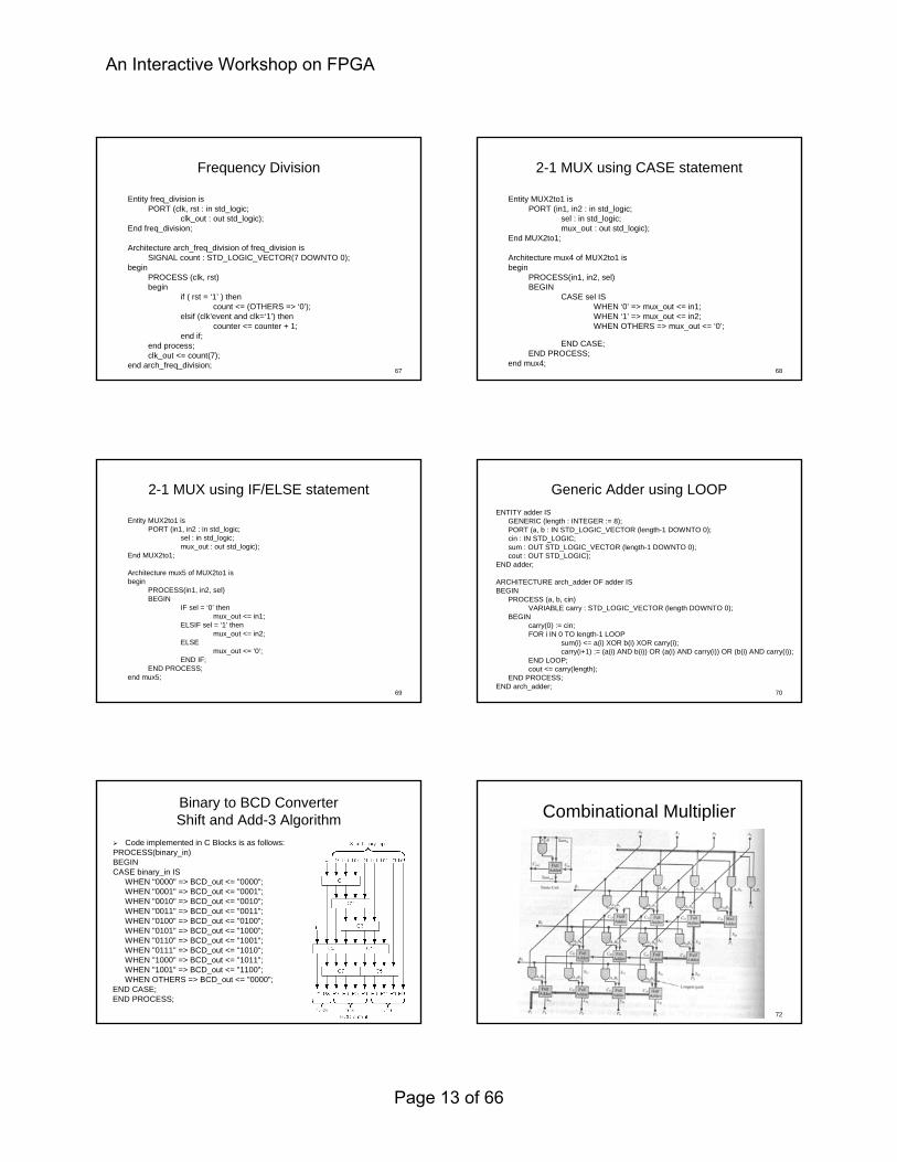
Frequency DivisionFrequency Division
Entity Entity freq_divisionfreq_division isisPORT (PORT (clkclk, , rstrst : in : in std_logicstd_logic;;
clk_outclk_out : out : out std_logicstd_logic););End End freq_divisionfreq_division;;
Architecture Architecture arch_freq_divisionarch_freq_division of of freq_divisionfreq_division isisSIGNAL count : STD_LOGIC_VECTOR(7 DOWNTO 0);SIGNAL count : STD_LOGIC_VECTOR(7 DOWNTO 0);
beginbeginPROCESS (PROCESS (clkclk, , rstrst))beginbegin
if ( if ( rstrst = = ‘‘11’’ ) then) thencount <= (OTHERS => count <= (OTHERS => ‘‘00’’););
elsifelsif ((clkclk’’eventevent and and clkclk==‘‘11’’) then) thencounter <= counter <= countercounter + 1;+ 1;
end if;end if;end process;end process;clk_outclk_out <= count(7);<= count(7);
end end arch_freq_divisionarch_freq_division;;6868
22--1 MUX using CASE statement1 MUX using CASE statement
Entity MUX2to1 isEntity MUX2to1 isPORT (in1, in2 : in PORT (in1, in2 : in std_logicstd_logic;;
selsel : in : in std_logicstd_logic;;mux_outmux_out : out : out std_logicstd_logic););
End MUX2to1;End MUX2to1;
Architecture mux4 of MUX2to1 isArchitecture mux4 of MUX2to1 isbeginbegin
PROCESS(in1, in2, sel)PROCESS(in1, in2, sel)BEGINBEGIN
CASE CASE selsel ISISWHEN WHEN ‘‘00’’ => => mux_outmux_out <= in1;<= in1;WHEN WHEN ‘‘11’’ => => mux_outmux_out <= in2;<= in2;WHEN OTHERS => WHEN OTHERS => mux_outmux_out <= <= ‘‘00’’;;
END CASE;END CASE;END PROCESS;END PROCESS;
end mux4;end mux4;
6969
22--1 MUX using IF/ELSE statement1 MUX using IF/ELSE statement
Entity MUX2to1 isEntity MUX2to1 isPORT (in1, in2 : in PORT (in1, in2 : in std_logicstd_logic;;
selsel : in : in std_logicstd_logic;;mux_outmux_out : out : out std_logicstd_logic););
End MUX2to1;End MUX2to1;
Architecture mux5 of MUX2to1 isArchitecture mux5 of MUX2to1 isbeginbegin
PROCESS(in1, in2, sel)PROCESS(in1, in2, sel)BEGINBEGIN
IF IF selsel = = ‘‘00’’ thenthenmux_outmux_out <= in1;<= in1;
ELSIF ELSIF selsel = = ‘‘11’’ thenthenmux_outmux_out <= in2;<= in2;
ELSEELSEmux_outmux_out <= <= ‘‘00’’;;
END IF;END IF;END PROCESS;END PROCESS;
end mux5;end mux5;
7070
Generic Adder using LOOPGeneric Adder using LOOPENTITY adder ISENTITY adder IS
GENERIC (length : INTEGER := 8);GENERIC (length : INTEGER := 8);PORT (a, b : IN STD_LOGIC_VECTOR (lengthPORT (a, b : IN STD_LOGIC_VECTOR (length--1 DOWNTO 0);1 DOWNTO 0);cincin : IN STD_LOGIC;: IN STD_LOGIC;sum : OUT STD_LOGIC_VECTOR (lengthsum : OUT STD_LOGIC_VECTOR (length--1 DOWNTO 0);1 DOWNTO 0);coutcout : OUT STD_LOGIC);: OUT STD_LOGIC);
END adder;END adder;
ARCHITECTURE ARCHITECTURE arch_adderarch_adder OF adder ISOF adder ISBEGINBEGIN
PROCESS (a, b, PROCESS (a, b, cincin))VARIABLE carry : STD_LOGIC_VECTOR (length DOWNTO 0);VARIABLE carry : STD_LOGIC_VECTOR (length DOWNTO 0);
BEGINBEGINcarry(0) := carry(0) := cincin;;FOR i IN 0 TO lengthFOR i IN 0 TO length--1 LOOP1 LOOP
sum(isum(i) <= ) <= a(ia(i) XOR ) XOR b(ib(i) XOR ) XOR carry(icarry(i););carry(i+1) := (carry(i+1) := (a(ia(i) AND ) AND b(ib(i)) OR ()) OR (a(ia(i) AND ) AND carry(icarry(i)) OR ()) OR (b(ib(i) AND ) AND carry(icarry(i));));
END LOOP;END LOOP;coutcout <= <= carry(lengthcarry(length););
END PROCESS;END PROCESS;END END arch_adderarch_adder;;
7171
Binary to BCD ConverterBinary to BCD ConverterShift and AddShift and Add--3 Algorithm3 Algorithm
Code implemented in C Blocks is as follows:Code implemented in C Blocks is as follows:PROCESS(binary_inPROCESS(binary_in))BEGINBEGINCASE CASE binary_inbinary_in ISIS
WHEN "0000" => WHEN "0000" => BCD_outBCD_out <= "0000";<= "0000";WHEN "0001" => WHEN "0001" => BCD_outBCD_out <= "0001";<= "0001";WHEN "0010" => WHEN "0010" => BCD_outBCD_out <= "0010";<= "0010";WHEN "0011" => WHEN "0011" => BCD_outBCD_out <= "0011";<= "0011";WHEN "0100" => WHEN "0100" => BCD_outBCD_out <= "0100";<= "0100";WHEN "0101" => WHEN "0101" => BCD_outBCD_out <= "1000";<= "1000";WHEN "0110" => WHEN "0110" => BCD_outBCD_out <= "1001";<= "1001";WHEN "0111" => WHEN "0111" => BCD_outBCD_out <= "1010";<= "1010";WHEN "1000" => WHEN "1000" => BCD_outBCD_out <= "1011";<= "1011";WHEN "1001" => WHEN "1001" => BCD_outBCD_out <= "1100";<= "1100";WHEN OTHERS => WHEN OTHERS => BCD_outBCD_out <= "0000";<= "0000";
END CASE;END CASE;END PROCESS;END PROCESS;
7272
Combinational MultiplierCombinational Multiplier
An Interactive Workshop on FPGA
Page 13 of 66
7373
Booth MultiplierBooth Multiplier
7474
Bad ProgramBad ProgramProcess(clkProcess(clk))BEGINBEGINIF (clkIF (clk’’EVENT AND clk=EVENT AND clk=’’11’’) THEN) THEN
small<=list (i);small<=list (i);pos<=i;pos<=i;IF (small >list (j)) THENIF (small >list (j)) THEN
small<=list (j);small<=list (j);pos<=j;pos<=j;
END IF;END IF;list (pos)<=list (i);list (pos)<=list (i);list (i)<=small;list (i)<=small;i<=i+1;i<=i+1;
END IF;END IF;END PROCESS;END PROCESS;
7575
Shift Operation using FOR LoopShift Operation using FOR LoopLeft shifting a signal which is defined as Left shifting a signal which is defined as ’’SIGNAL x : STD_LOGIC_VECTOR(6 DOWNTO 0);SIGNAL x : STD_LOGIC_VECTOR(6 DOWNTO 0);’’
PROCESS(clk)BEGIN
x(6) <= x(5);x(5) <= x(4);x(4) <= x(3);x(3) <= x(2);x(2) <= x(1);x(1) <= x(0);x(0) <= ’0’;
END PROCESS;
PROCESS(clk)PROCESS(clk)BEGINBEGINFOR i IN 0 TO 5 LOOPFOR i IN 0 TO 5 LOOP
x(i+1) <= x(i);x(i+1) <= x(i);END LOOP;END LOOP;x(0) <= x(0) <= ’’00’’;;END PROCESS;END PROCESS;
Equavalent Code
An Interactive Workshop on FPGA
Page 14 of 66

Introduction to Modelsim
An Interactive Workshop on FPGA
Page 15 of 66

Step 1: Launch the ModelSim 5.7f Simulator.
• Open the ModelSim 5.7f software: Go to Start Menu Programs ModelSim SE 5.7f ModelSim
• Go to File New Project (the following dialogue box will appear)
Figure 1: Starting New Project • Write the project name and click OK. • After clicking OK, the following small window will appear
Figure 2: Adding a new/existing file to project
After selecting Create New File another window will appear
An Interactive Workshop on FPGA
Page 16 of 66
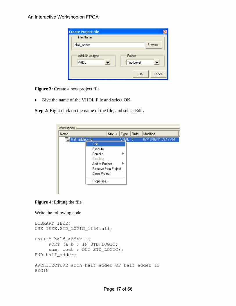
Figure 3: Create a new project file • Give the name of the VHDL File and select OK. Step 2: Right click on the name of the file, and select Edit.
Figure 4: Editing the file
Write the following code
LIBRARY IEEE; USE IEEE.STD_LOGIC_1164.all; ENTITY half_adder IS PORT (a,b : IN STD_LOGIC; sum, cout : OUT STD_LOGIC); END half_adder; ARCHITECTURE arch_half_adder OF half_adder IS BEGIN
An Interactive Workshop on FPGA
Page 17 of 66
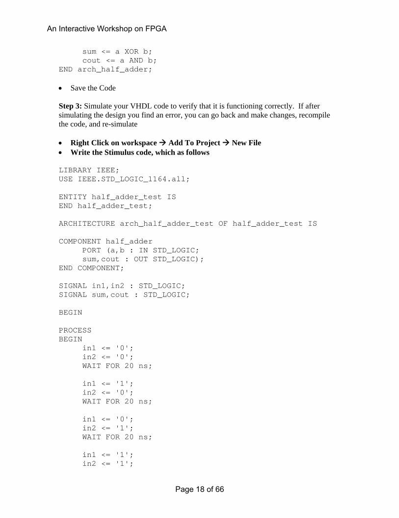
sum <= a XOR b; cout <= a AND b; END arch_half_adder;
• Save the Code Step 3: Simulate your VHDL code to verify that it is functioning correctly. If after simulating the design you find an error, you can go back and make changes, recompile the code, and re-simulate
• Right Click on workspace Add To Project New File • Write the Stimulus code, which as follows LIBRARY IEEE; USE IEEE.STD_LOGIC_1164.all; ENTITY half_adder_test IS END half_adder_test; ARCHITECTURE arch_half_adder_test OF half_adder_test IS COMPONENT half_adder PORT (a,b : IN STD_LOGIC; sum,cout : OUT STD_LOGIC); END COMPONENT; SIGNAL in1,in2 : STD_LOGIC; SIGNAL sum,cout : STD_LOGIC; BEGIN PROCESS BEGIN in1 <= '0'; in2 <= '0'; WAIT FOR 20 ns; in1 <= '1'; in2 <= '0'; WAIT FOR 20 ns; in1 <= '0'; in2 <= '1'; WAIT FOR 20 ns; in1 <= '1'; in2 <= '1';
An Interactive Workshop on FPGA
Page 18 of 66

WAIT FOR 20 ns; END PROCESS; U1: half_adder PORT MAP (in1, in2, sum, cout); END arch_half_adder_test; • Compile all the files(if an error occurs edit that particular file) • Now click on menu Simulate Simulate, following window will appear
Figure 5: Simulate
• Select the work and the test file. Then click OK. • The design will be loaded. • Now Select the Simulation Run Run All • The results will be displayed in the text form. • To, view the wave forms click on View Signal, and View Wave. • The following windows will appear.
An Interactive Workshop on FPGA
Page 19 of 66
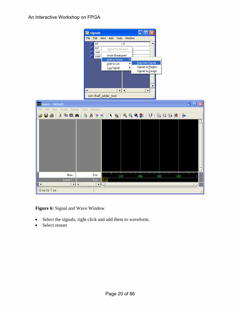
Figure 6: Signal and Wave Window • Select the signals, right click and add them to waveform. • Select restart
An Interactive Workshop on FPGA
Page 20 of 66
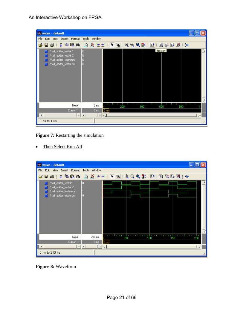
Figure 7: Restarting the simulation • Then Select Run All
Figure 8: Waveform
An Interactive Workshop on FPGA
Page 21 of 66
SPARTAN XCS 10 TUTORIAL
Using Xilinx 4.1i
An Interactive Workshop on FPGA
Page 22 of 66
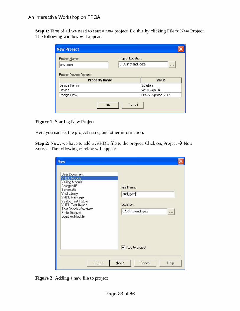
Step 1: First of all we need to start a new project. Do this by clicking File New Project. The following window will appear.
Figure 1: Starting New Project Here you can set the project name, and other information. Step 2: Now, we have to add a .VHDL file to the project. Click on, Project New Source. The following window will appear.
Figure 2: Adding a new file to project
An Interactive Workshop on FPGA
Page 23 of 66
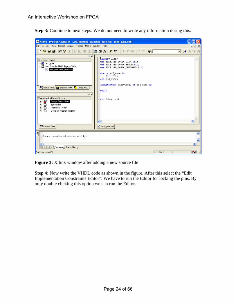
Step 3: Continue to next steps. We do not need to write any information during this.
Figure 3: Xilinx window after adding a new source file Step 4: Now write the VHDL code as shown in the figure. After this select the “Edit Implementation Constraints Editor”. We have to run the Editor for locking the pins. By only double clicking this option we can run the Editor.
An Interactive Workshop on FPGA
Page 24 of 66

Figrue 4: Edit Implementation Constraints A new window will be opened. We have to lock the pins according to the Spartan I/Os. The following are the pin numbers which we have assigned to our modules inputs and output. All the inputs are connected to the switches on the Board and the we assign the output to an LED. The format for writing the pin number is e.g, A p28. You have to save this file and the close the Editor and return to the XILINX main window.
An Interactive Workshop on FPGA
Page 25 of 66

Figure 5: Pin Assignments Step 5: After giving the pin configuration run the synthesize command by simply double clicking it or by selecting the synthesize option and then using the run command. The green TICK on the ‘Synthesize’ button will indicate correct syntheses. Step 6: After this double click the ‘Implement Design’ option. Green TICK on the Implement button will indicate correct Implementation. Step 7: The next step is to generate a bit file which can be downloaded in the FPGA. This can be easily done by simply double clicking the ‘Generate Programming File’ option. If the bit file is generated successfully you will see the same green TICK on it.
An Interactive Workshop on FPGA
Page 26 of 66
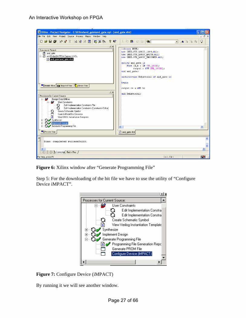
Figure 6: Xilinx window after “Generate Programming File” Step 5: For the downloading of the bit file we have to use the utility of “Configure Device iMPACT”.
Figure 7: Configure Device (iMPACT) By running it we will see another window.
An Interactive Workshop on FPGA
Page 27 of 66
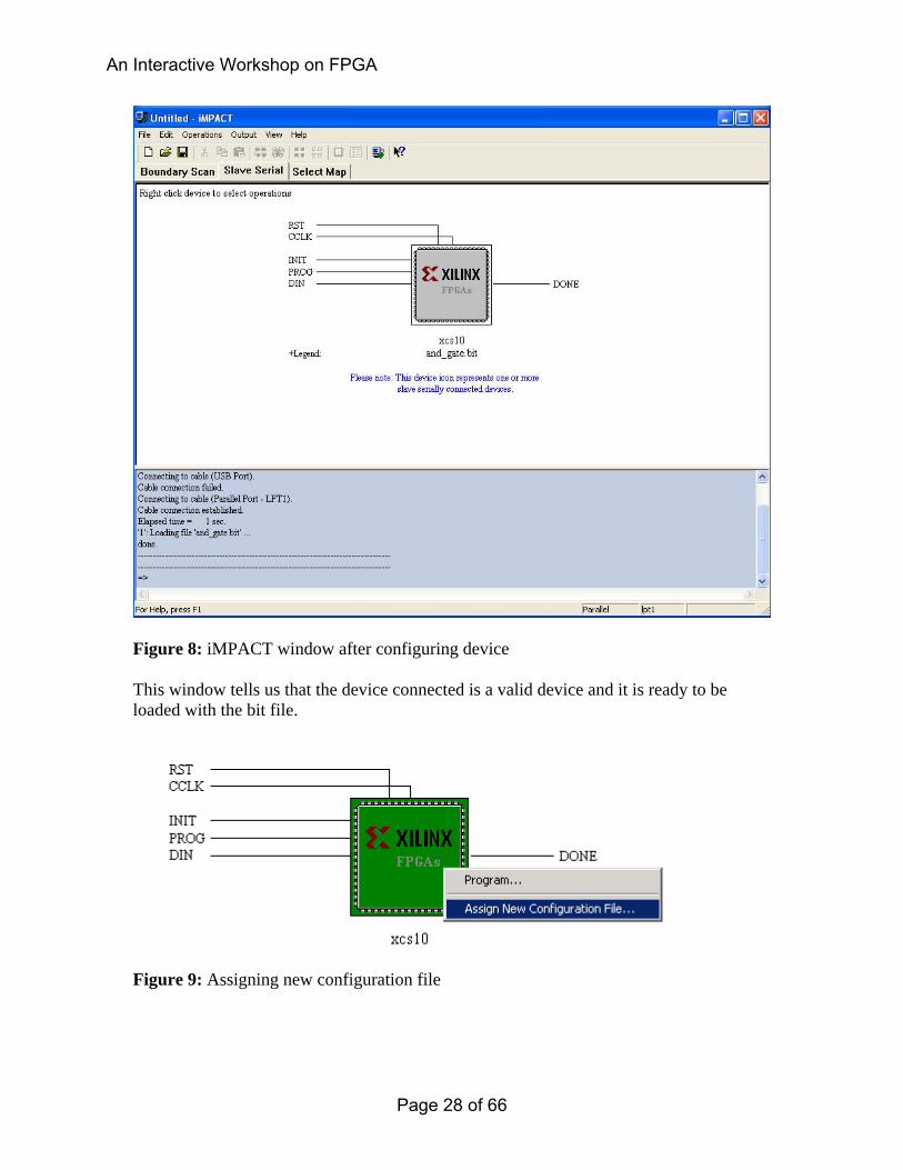
Figure 8: iMPACT window after configuring device This window tells us that the device connected is a valid device and it is ready to be loaded with the bit file.
Figure 9: Assigning new configuration file
An Interactive Workshop on FPGA
Page 28 of 66
By right clicking on the device icon we get two options: 1 Program 2 Assign New Configuration File…
If no configuration file is assigned or if you want to assign a new configuration file then select the 2nd option. A browser window will be opened and from here you can select the bit file which you want to down load in the FPGA. In this example the bit file Name is “and_gate.bit”. After selecting the bit file you have to Program the device. After the successful downloading has been done you will be given a success message.
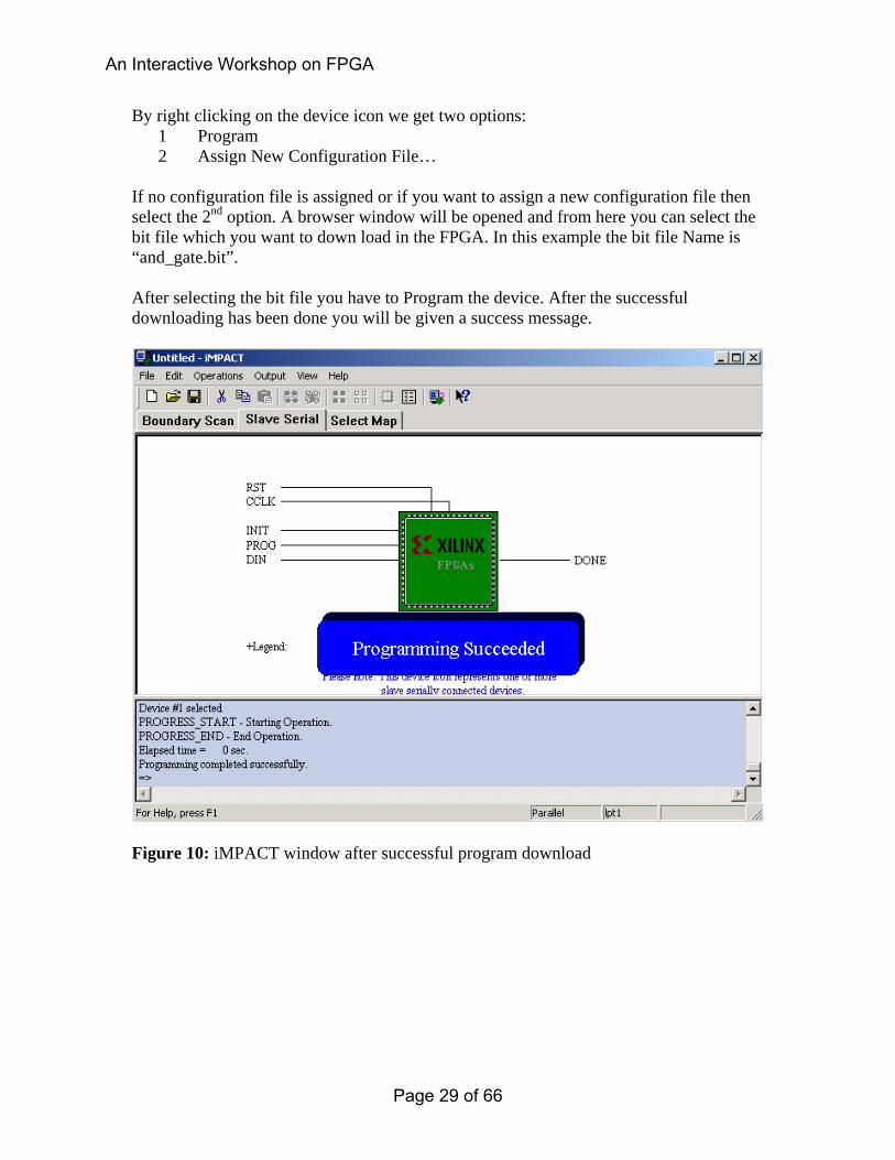
Figure 10: iMPACT window after successful program download
An Interactive Workshop on FPGA
Page 29 of 66

THE VHDL CODE: library IEEE; use IEEE.STD_LOGIC_1164.ALL; use IEEE.STD_LOGIC_ARITH.ALL; use IEEE.STD_LOGIC_UNSIGNED.ALL; ENTITY and_gate IS PORT (a,b : IN STD_LOGIC; output : OUT STD_LOGIC); END and_gate; ARCHITECTURE Behavioral OF and_gate IS BEGIN output <= a AND b; END Behavioral;
An Interactive Workshop on FPGA
Page 30 of 66
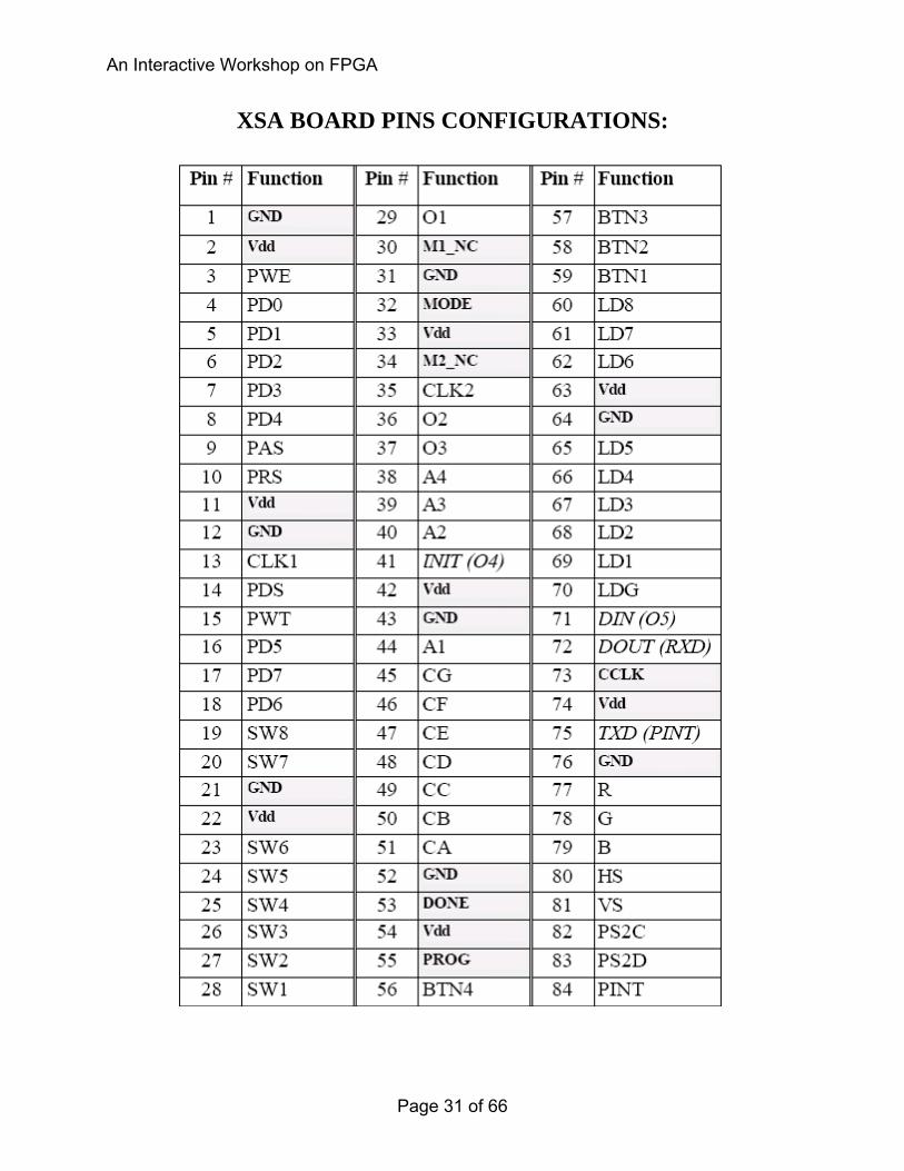
XSA BOARD PINS CONFIGURATIONS:
An Interactive Workshop on FPGA
Page 31 of 66

LAB # 01 In this lab, we will design some small circuits in VHDL using the ModelSim tool. You will use a typical HDL flow, write the HDL code, and run a functional HDL simulation. • Half Adder • Full Adder • 4-bit Ripple Carry Adder (Structural) • 4-to-1 Multiplexer After completing this lab, you will be able to: • Perform the basic design flow for writing VHDL code using concurrent statements. • Understand the basic design for a testbench. • Simulate a VHDL file using Modelsim. • Analyze the simulation Results.
An Interactive Workshop on FPGA
Page 32 of 66
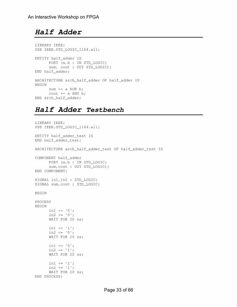
Half Adder LIBRARY IEEE; USE IEEE.STD_LOGIC_1164.all; ENTITY half_adder IS PORT (a,b : IN STD_LOGIC; sum, cout : OUT STD_LOGIC); END half_adder; ARCHITECTURE arch_half_adder OF half_adder IS BEGIN sum <= a XOR b; cout <= a AND b; END arch_half_adder; Half Adder Testbench LIBRARY IEEE; USE IEEE.STD_LOGIC_1164.all; ENTITY half_adder_test IS END half_adder_test; ARCHITECTURE arch_half_adder_test OF half_adder_test IS COMPONENT half_adder PORT (a,b : IN STD_LOGIC; sum,cout : OUT STD_LOGIC); END COMPONENT; SIGNAL in1,in2 : STD_LOGIC; SIGNAL sum,cout : STD_LOGIC; BEGIN PROCESS BEGIN in1 <= '0'; in2 <= '0'; WAIT FOR 20 ns; in1 <= '1'; in2 <= '0'; WAIT FOR 20 ns; in1 <= '0'; in2 <= '1'; WAIT FOR 20 ns; in1 <= '1'; in2 <= '1'; WAIT FOR 20 ns; END PROCESS;
An Interactive Workshop on FPGA
Page 33 of 66

U1: half_adder PORT MAP (in1, in2, sum, cout); END arch_half_adder_test;
An Interactive Workshop on FPGA
Page 34 of 66
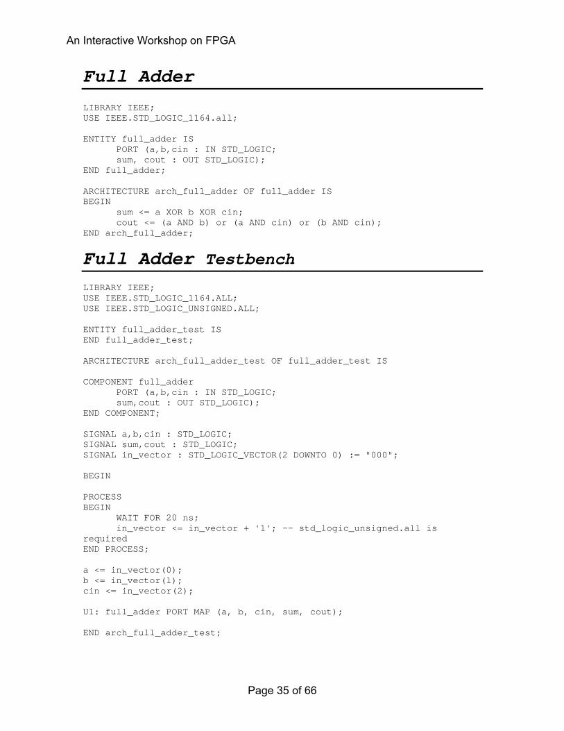
Full Adder LIBRARY IEEE; USE IEEE.STD_LOGIC_1164.all; ENTITY full_adder IS PORT (a,b,cin : IN STD_LOGIC; sum, cout : OUT STD_LOGIC); END full_adder; ARCHITECTURE arch_full_adder OF full_adder IS BEGIN sum <= a XOR b XOR cin; cout <= (a AND b) or (a AND cin) or (b AND cin); END arch_full_adder;
Full Adder Testbench LIBRARY IEEE; USE IEEE.STD_LOGIC_1164.ALL; USE IEEE.STD_LOGIC_UNSIGNED.ALL; ENTITY full_adder_test IS END full_adder_test; ARCHITECTURE arch_full_adder_test OF full_adder_test IS COMPONENT full_adder PORT (a,b,cin : IN STD_LOGIC; sum,cout : OUT STD_LOGIC); END COMPONENT; SIGNAL a,b,cin : STD_LOGIC; SIGNAL sum,cout : STD_LOGIC; SIGNAL in_vector : STD_LOGIC_VECTOR(2 DOWNTO 0) := "000"; BEGIN PROCESS BEGIN WAIT FOR 20 ns; in_vector <= in_vector + '1'; -- std_logic_unsigned.all is required END PROCESS; a <= in_vector(0); b <= in_vector(1); cin <= in_vector(2); U1: full_adder PORT MAP (a, b, cin, sum, cout); END arch_full_adder_test;
An Interactive Workshop on FPGA
Page 35 of 66

4-bit RCA (Structural) LIBRARY IEEE; USE IEEE.STD_LOGIC_1164.all; ENTITY RCA_4bit IS PORT (a,b : IN STD_LOGIC_VECTOR(3 DOWNTO 0); cin : IN STD_LOGIC; sum : OUT STD_LOGIC_VECTOR(3 DOWNTO 0); cout : OUT STD_LOGIC); END RCA_4bit; ARCHITECTURE arch_RCA_4bit OF RCA_4bit IS COMPONENT full_adder2 PORT (a,b,cin : IN STD_LOGIC; sum,cout : OUT STD_LOGIC); END COMPONENT; SIGNAL c1, c2, c3 : STD_LOGIC; BEGIN f_adder1: full_adder2 PORT MAP (a(0), b(0), cin, sum(0), c1); f_adder2: full_adder2 PORT MAP (a(1), b(1), c1, sum(1), c2); f_adder3: full_adder2 PORT MAP (a(2), b(2), c2, sum(2), c3); f_adder4: full_adder2 PORT MAP (a(3), b(3), c3, sum(3), cout); END arch_RCA_4bit;
4-bit RCA Testbench LIBRARY IEEE; USE IEEE.STD_LOGIC_1164.ALL; USE IEEE.STD_LOGIC_UNSIGNED.ALL; ENTITY RCA_4bit_test IS END RCA_4bit_test; ARCHITECTURE arch_RCA_4bit_test OF RCA_4bit_test IS COMPONENT RCA_4bit PORT (a,b : IN STD_LOGIC_VECTOR(3 DOWNTO 0); cin : IN STD_LOGIC; sum : OUT STD_LOGIC_VECTOR(3 DOWNTO 0); cout : OUT STD_LOGIC); END COMPONENT; SIGNAL a,b : STD_LOGIC_VECTOR(3 DOWNTO 0) := "0000"; SIGNAL cin : STD_LOGIC; SIGNAL sum : STD_LOGIC_VECTOR(3 DOWNTO 0); SIGNAL cout : STD_LOGIC; BEGIN
An Interactive Workshop on FPGA
Page 36 of 66

input_a: PROCESS BEGIN WAIT FOR 20 ns; a <= a + '1'; -- std_logic_unsigned.all is required END PROCESS input_a; input_b: PROCESS BEGIN WAIT FOR 20 ns; b <= b + "0010"; -- std_logic_unsigned.all is required END PROCESS input_b; cin <= '0'; RCA_1: RCA_4bit PORT MAP (a, b, cin, sum, cout); END arch_RCA_4bit_test;
An Interactive Workshop on FPGA
Page 37 of 66
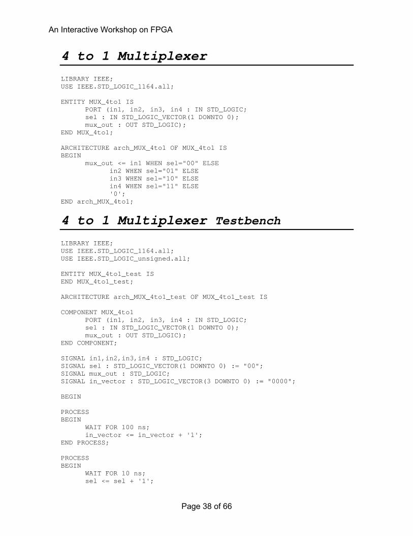
4 to 1 Multiplexer LIBRARY IEEE; USE IEEE.STD_LOGIC_1164.all; ENTITY MUX_4to1 IS PORT (in1, in2, in3, in4 : IN STD_LOGIC; sel : IN STD_LOGIC_VECTOR(1 DOWNTO 0); mux_out : OUT STD_LOGIC); END MUX_4to1; ARCHITECTURE arch_MUX_4to1 OF MUX_4to1 IS BEGIN mux_out <= in1 WHEN sel="00" ELSE in2 WHEN sel="01" ELSE in3 WHEN sel="10" ELSE in4 WHEN sel="11" ELSE '0'; END arch_MUX_4to1;
4 to 1 Multiplexer Testbench LIBRARY IEEE; USE IEEE.STD_LOGIC_1164.all; USE IEEE.STD_LOGIC_unsigned.all; ENTITY MUX_4to1_test IS END MUX_4to1_test; ARCHITECTURE arch_MUX_4to1_test OF MUX_4to1_test IS COMPONENT MUX_4to1 PORT (in1, in2, in3, in4 : IN STD_LOGIC; sel : IN STD_LOGIC_VECTOR(1 DOWNTO 0); mux_out : OUT STD_LOGIC); END COMPONENT; SIGNAL in1,in2,in3,in4 : STD_LOGIC; SIGNAL sel : STD_LOGIC_VECTOR(1 DOWNTO 0) := "00"; SIGNAL mux_out : STD_LOGIC; SIGNAL in_vector : STD_LOGIC_VECTOR(3 DOWNTO 0) := "0000"; BEGIN PROCESS BEGIN WAIT FOR 100 ns; in_vector <= in_vector + '1'; END PROCESS; PROCESS BEGIN WAIT FOR 10 ns; sel <= sel + '1';
An Interactive Workshop on FPGA
Page 38 of 66

END PROCESS; (in1,in2,in3,in4) <= in_vector; mux1: MUX_4to1 PORT MAP (in1, in2, in3, in4, sel, mux_out); END arch_MUX_4to1_test;
An Interactive Workshop on FPGA
Page 39 of 66
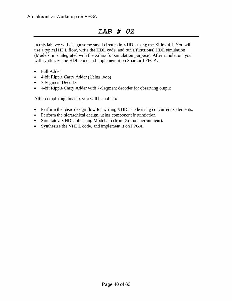
LAB # 02 In this lab, we will design some small circuits in VHDL using the Xilinx 4.1. You will use a typical HDL flow, write the HDL code, and run a functional HDL simulation (Modelsim is integrated with the Xilinx for simulation purpose). After simulation, you will synthesize the HDL code and implement it on Spartan-I FPGA. • Full Adder • 4-bit Ripple Carry Adder (Using loop) • 7-Segment Decoder • 4-bit Ripple Carry Adder with 7-Segment decoder for observing output After completing this lab, you will be able to: • Perform the basic design flow for writing VHDL code using concurrent statements. • Perform the hierarchical design, using component instantiation. • Simulate a VHDL file using Modelsim (from Xilinx environment). • Synthesize the VHDL code, and implement it on FPGA.
An Interactive Workshop on FPGA
Page 40 of 66

Full Adder (Structural) LIBRARY IEEE; USE IEEE.STD_LOGIC_1164.all; ENTITY full_adder2 IS PORT (a,b,cin : IN STD_LOGIC; sum, cout : OUT STD_LOGIC); END full_adder2; ARCHITECTURE arch_full_adder2 OF full_adder2 IS COMPONENT half_adder PORT (a,b : IN STD_LOGIC; sum,cout : OUT STD_LOGIC); END COMPONENT; SIGNAL w1, w2, w3 : STD_LOGIC; BEGIN h_adder1: half_adder PORT MAP (a, b, w1, w3); h_adder2: half_adder PORT MAP (w1, cin, sum, w2); cout <= w2 OR w3; END arch_full_adder2;
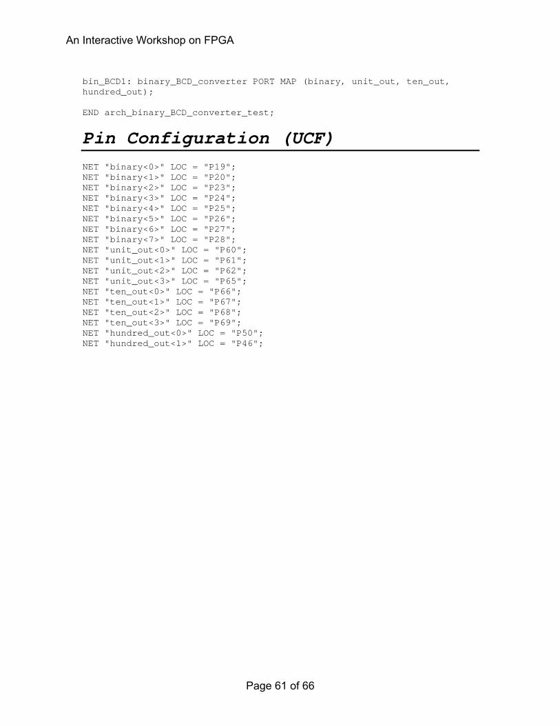
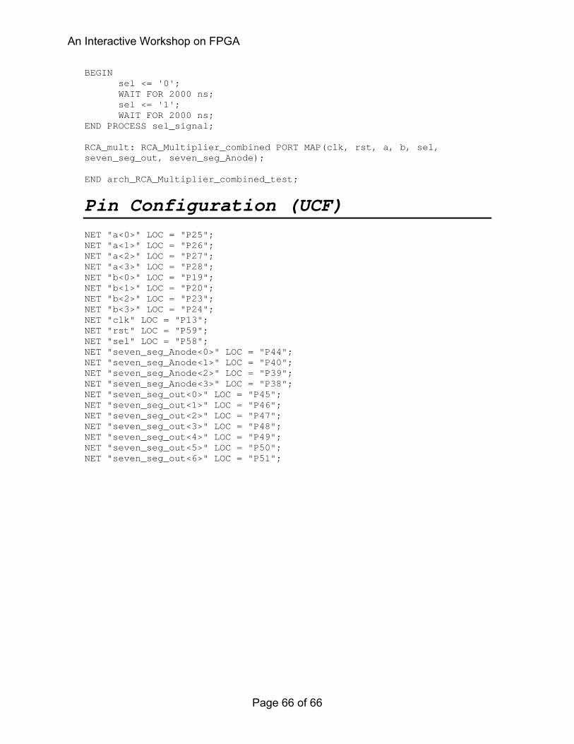
Pin Configuration (UCF) NET "a" LOC = "P28"; NET "b" LOC = "P27"; NET "cin" LOC = "P26"; NET "cout" LOC = "P69"; NET "sum" LOC = "P68";
An Interactive Workshop on FPGA
Page 41 of 66

4-bit RCA (using loop) LIBRARY IEEE; USE IEEE.STD_LOGIC_1164.all; ENTITY RCA_4bit_2 IS GENERIC (length : INTEGER := 4); PORT (a,b : IN STD_LOGIC_VECTOR(length-1 DOWNTO 0); cin : IN STD_LOGIC; sum : OUT STD_LOGIC_VECTOR(length-1 DOWNTO 0); cout : OUT STD_LOGIC); END RCA_4bit_2; ARCHITECTURE arch_RCA_4bit_2 OF RCA_4bit_2 IS BEGIN PROCESS (a, b, cin) VARIABLE carry : STD_LOGIC_VECTOR (length DOWNTO 0); BEGIN carry(0) := cin; FOR i IN 0 TO length-1 LOOP sum(i) <= a(i) XOR b(i) XOR carry(i); carry(i+1) := (a(i) AND b(i)) OR (a(i) AND carry(i)) OR (b(i) AND carry(i)); END LOOP; cout <= carry(length); END PROCESS; END arch_RCA_4bit_2;
Pin Configuration (UCF) NET "a<0>" LOC = "P25"; NET "a<1>" LOC = "P26"; NET "a<2>" LOC = "P27"; NET "a<3>" LOC = "P28"; NET "b<0>" LOC = "P19"; NET "b<1>" LOC = "P20"; NET "b<2>" LOC = "P23"; NET "b<3>" LOC = "P24"; NET "cin" LOC = "P59"; NET "cout" LOC = "P66"; NET "sum<0>" LOC = "P60"; NET "sum<1>" LOC = "P61"; NET "sum<2>" LOC = "P62"; NET "sum<3>" LOC = "P65";
An Interactive Workshop on FPGA
Page 42 of 66
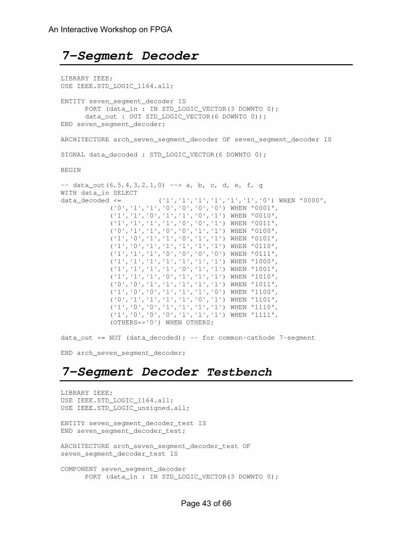
7-Segment Decoder LIBRARY IEEE; USE IEEE.STD_LOGIC_1164.all; ENTITY seven_segment_decoder IS PORT (data_in : IN STD_LOGIC_VECTOR(3 DOWNTO 0); data_out : OUT STD_LOGIC_VECTOR(6 DOWNTO 0)); END seven_segment_decoder; ARCHITECTURE arch_seven_segment_decoder OF seven_segment_decoder IS SIGNAL data_decoded : STD_LOGIC_VECTOR(6 DOWNTO 0); BEGIN -- data_out(6,5,4,3,2,1,0) --> a, b, c, d, e, f, g WITH data_in SELECT data_decoded <= ('1','1','1','1','1','1','0') WHEN "0000", ('0','1','1','0','0','0','0') WHEN "0001", ('1','1','0','1','1','0','1') WHEN "0010", ('1','1','1','1','0','0','1') WHEN "0011", ('0','1','1','0','0','1','1') WHEN "0100", ('1','0','1','1','0','1','1') WHEN "0101", ('1','0','1','1','1','1','1') WHEN "0110", ('1','1','1','0','0','0','0') WHEN "0111", ('1','1','1','1','1','1','1') WHEN "1000", ('1','1','1','1','0','1','1') WHEN "1001", ('1','1','1','0','1','1','1') WHEN "1010", ('0','0','1','1','1','1','1') WHEN "1011", ('1','0','0','1','1','1','0') WHEN "1100", ('0','1','1','1','1','0','1') WHEN "1101", ('1','0','0','1','1','1','1') WHEN "1110", ('1','0','0','0','1','1','1') WHEN "1111", (OTHERS=>'0') WHEN OTHERS; data_out <= NOT (data_decoded); -- for common-cathode 7-segment END arch_seven_segment_decoder;
7-Segment Decoder Testbench LIBRARY IEEE; USE IEEE.STD_LOGIC_1164.all; USE IEEE.STD_LOGIC_unsigned.all; ENTITY seven_segment_decoder_test IS END seven_segment_decoder_test; ARCHITECTURE arch_seven_segment_decoder_test OF seven_segment_decoder_test IS COMPONENT seven_segment_decoder PORT (data_in : IN STD_LOGIC_VECTOR(3 DOWNTO 0);
An Interactive Workshop on FPGA
Page 43 of 66
data_out : OUT STD_LOGIC_VECTOR(6 DOWNTO 0)); END COMPONENT; SIGNAL data_in : STD_LOGIC_VECTOR(3 DOWNTO 0) := "0000"; SIGNAL data_out : STD_LOGIC_VECTOR(6 DOWNTO 0); BEGIN PROCESS BEGIN WAIT FOR 10 ns; data_in <= data_in + '1'; END PROCESS; seven_seg1: seven_segment_decoder PORT MAP (data_in, data_out); END arch_seven_segment_decoder_test;
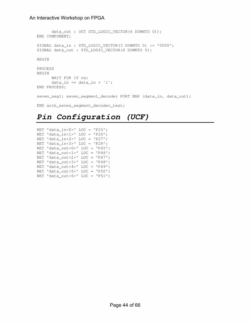
Pin Configuration (UCF) NET "data_in<0>" LOC = "P25"; NET "data_in<1>" LOC = "P26"; NET "data_in<2>" LOC = "P27"; NET "data_in<3>" LOC = "P28"; NET "data_out<0>" LOC = "P45"; NET "data_out<1>" LOC = "P46"; NET "data_out<2>" LOC = "P47"; NET "data_out<3>" LOC = "P48"; NET "data_out<4>" LOC = "P49"; NET "data_out<5>" LOC = "P50"; NET "data_out<6>" LOC = "P51";
An Interactive Workshop on FPGA
Page 44 of 66
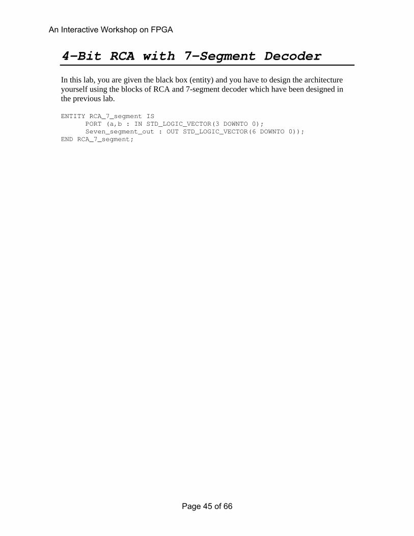
4-Bit RCA with 7-Segment Decoder In this lab, you are given the black box (entity) and you have to design the architecture yourself using the blocks of RCA and 7-segment decoder which have been designed in the previous lab. ENTITY RCA_7_segment IS PORT (a,b : IN STD_LOGIC_VECTOR(3 DOWNTO 0); Seven_segment_out : OUT STD_LOGIC_VECTOR(6 DOWNTO 0)); END RCA_7_segment;
An Interactive Workshop on FPGA
Page 45 of 66

LAB # 03 In this lab, we will design sequential circuits in VHDL using the Xilinx 4.1. You will use a typical HDL flow, write the HDL code, and run a functional HDL simulation (Modelsim is integrated with the Xilinx for simulation purpose). After simulation, you will synthesize the HDL code and implement it on Spartan-I FPGA. • Frequency Divider (LED Flasher) • 4-bit Counter • 4-bit Combinational Multiplier After completing this lab, you will be able to: • Perform the basic design flow for writing VHDL code using concurrent and
sequential statements (Inside a Process). • Understand of how to design a positive-edge or negative-edge flip-flop. • Understand the working of a Process. • Synthesize the VHDL code, and implement it on FPGA.
An Interactive Workshop on FPGA
Page 46 of 66

Frequency Divisor (LED Flasher) LIBRARY IEEE; USE IEEE.STD_LOGIC_1164.all; USE IEEE.STD_LOGIC_UNSIGNED.all; ENTITY freq_division IS PORT (clk_in, rst : IN STD_LOGIC; clk_out : OUT STD_LOGIC); END freq_division; ARCHITECTURE arch_freq_division OF freq_division IS SIGNAL counter : STD_LOGIC_VECTOR(25 DOWNTO 0); SIGNAL clk2 : STD_LOGIC; BEGIN PROCESS (clk_in,rst) BEGIN IF(rst='1') THEN counter <= (OTHERS=>'0'); clk2 <= '0'; ELSIF (clk_in'EVENT AND clk_in='1') THEN IF(counter=12500000) THEN counter <= (OTHERS=>'0'); clk2 <= NOT clk2; ELSE counter <= counter + '1'; END IF; END IF; END PROCESS; clk_out <= clk2; END arch_freq_division;
Frequency Divisor Testbench LIBRARY IEEE; USE IEEE.STD_LOGIC_1164.all; USE IEEE.STD_LOGIC_unsigned.all; ENTITY freq_division_test IS END freq_division_test; ARCHITECTURE arch_freq_division_test OF freq_division_test IS COMPONENT freq_division PORT (clk_in, rst : IN STD_LOGIC; clk_out : OUT STD_LOGIC); END COMPONENT; SIGNAL clk_in, rst : STD_LOGIC := '0';
An Interactive Workshop on FPGA
Page 47 of 66

SIGNAL clk_out : STD_LOGIC; BEGIN clk_gen: PROCESS BEGIN LOOP WAIT FOR 20 ns; clk_in <= NOT clk_in; END LOOP; END PROCESS clk_gen; rst_gen: PROCESS BEGIN rst <= '1'; WAIT FOR 30 ns; rst <= '0'; WAIT; END PROCESS rst_gen; freq_div: freq_division PORT MAP (clk_in, rst, clk_out); END arch_freq_division_test;
Pin Configuration (UCF) Since no system reset is available on the board, so we will use a push button as reset. NET "clk_in" LOC = "P13"; NET "clk_out" LOC = "P69"; NET "rst" LOC = "P59";
An Interactive Workshop on FPGA
Page 48 of 66
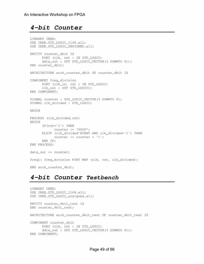
4-bit Counter LIBRARY IEEE; USE IEEE.STD_LOGIC_1164.all; USE IEEE.STD_LOGIC_UNSIGNED.all; ENTITY counter_4bit IS PORT (clk, rst : IN STD_LOGIC; data_out : OUT STD_LOGIC_VECTOR(3 DOWNTO 0)); END counter_4bit; ARCHITECTURE arch_counter_4bit OF counter_4bit IS COMPONENT freq_division PORT (clk_in, rst : IN STD_LOGIC; clk_out : OUT STD_LOGIC); END COMPONENT; SIGNAL counter : STD_LOGIC_VECTOR(3 DOWNTO 0); SIGNAL clk_divided : STD_LOGIC; BEGIN PROCESS (clk_divided,rst) BEGIN IF(rst='1') THEN counter <= "0000"; ELSIF (clk_divided'EVENT AND clk_divided='1') THEN counter <= counter + '1'; END IF; END PROCESS; data_out <= counter; freq1: freq_division PORT MAP (clk, rst, clk_divided); END arch_counter_4bit; 4-bit Counter Testbench LIBRARY IEEE; USE IEEE.STD_LOGIC_1164.all; USE IEEE.STD_LOGIC_unsigned.all; ENTITY counter_4bit_test IS END counter_4bit_test; ARCHITECTURE arch_counter_4bit_test OF counter_4bit_test IS COMPONENT counter_4bit PORT (clk, rst : IN STD_LOGIC; data_out : OUT STD_LOGIC_VECTOR(3 DOWNTO 0)); END COMPONENT;
An Interactive Workshop on FPGA
Page 49 of 66
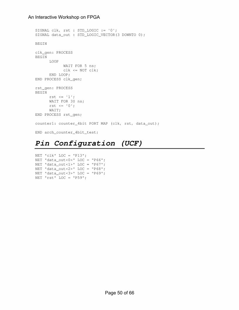
SIGNAL clk, rst : STD_LOGIC := '0'; SIGNAL data_out : STD_LOGIC_VECTOR(3 DOWNTO 0); BEGIN clk_gen: PROCESS BEGIN LOOP WAIT FOR 5 ns; clk <= NOT clk; END LOOP; END PROCESS clk_gen; rst_gen: PROCESS BEGIN rst <= '1'; WAIT FOR 30 ns; rst <= '0'; WAIT; END PROCESS rst_gen; counter1: counter_4bit PORT MAP (clk, rst, data_out); END arch_counter_4bit_test;
Pin Configuration (UCF) NET "clk" LOC = "P13"; NET "data_out<0>" LOC = "P66"; NET "data_out<1>" LOC = "P67"; NET "data_out<2>" LOC = "P68"; NET "data_out<3>" LOC = "P69"; NET "rst" LOC = "P59";
An Interactive Workshop on FPGA
Page 50 of 66
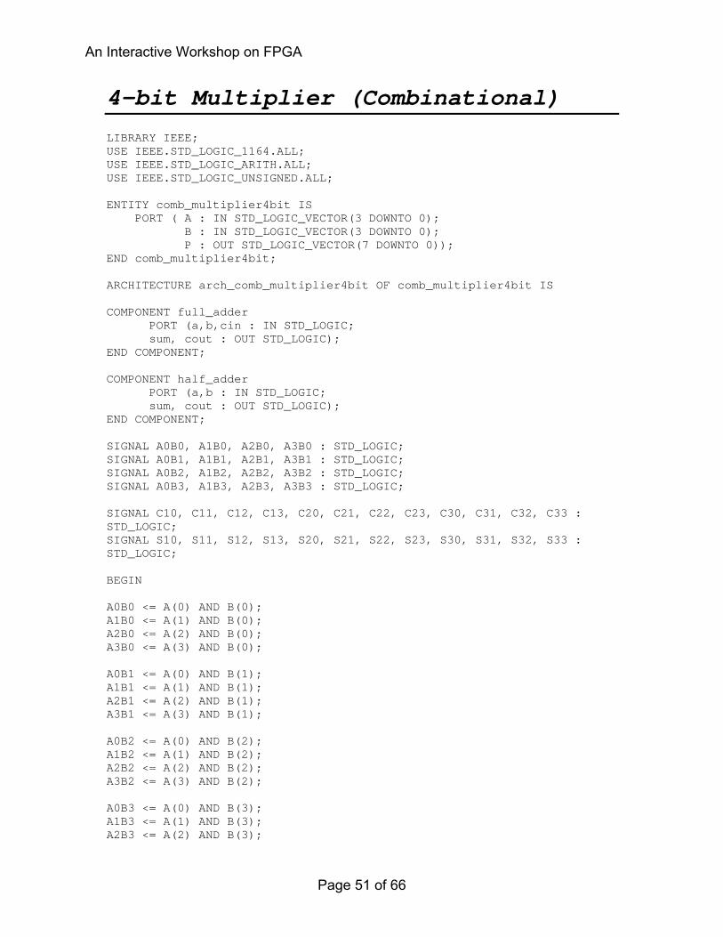
4-bit Multiplier (Combinational) LIBRARY IEEE; USE IEEE.STD_LOGIC_1164.ALL; USE IEEE.STD_LOGIC_ARITH.ALL; USE IEEE.STD_LOGIC_UNSIGNED.ALL; ENTITY comb_multiplier4bit IS PORT ( A : IN STD_LOGIC_VECTOR(3 DOWNTO 0); B : IN STD_LOGIC_VECTOR(3 DOWNTO 0); P : OUT STD_LOGIC_VECTOR(7 DOWNTO 0)); END comb_multiplier4bit; ARCHITECTURE arch_comb_multiplier4bit OF comb_multiplier4bit IS COMPONENT full_adder PORT (a,b,cin : IN STD_LOGIC; sum, cout : OUT STD_LOGIC); END COMPONENT; COMPONENT half_adder PORT (a,b : IN STD_LOGIC; sum, cout : OUT STD_LOGIC); END COMPONENT; SIGNAL A0B0, A1B0, A2B0, A3B0 : STD_LOGIC; SIGNAL A0B1, A1B1, A2B1, A3B1 : STD_LOGIC; SIGNAL A0B2, A1B2, A2B2, A3B2 : STD_LOGIC; SIGNAL A0B3, A1B3, A2B3, A3B3 : STD_LOGIC; SIGNAL C10, C11, C12, C13, C20, C21, C22, C23, C30, C31, C32, C33 : STD_LOGIC; SIGNAL S10, S11, S12, S13, S20, S21, S22, S23, S30, S31, S32, S33 : STD_LOGIC; BEGIN A0B0 <= A(0) AND B(0); A1B0 <= A(1) AND B(0); A2B0 <= A(2) AND B(0); A3B0 <= A(3) AND B(0); A0B1 <= A(0) AND B(1); A1B1 <= A(1) AND B(1); A2B1 <= A(2) AND B(1); A3B1 <= A(3) AND B(1); A0B2 <= A(0) AND B(2); A1B2 <= A(1) AND B(2); A2B2 <= A(2) AND B(2); A3B2 <= A(3) AND B(2); A0B3 <= A(0) AND B(3); A1B3 <= A(1) AND B(3); A2B3 <= A(2) AND B(3);
An Interactive Workshop on FPGA
Page 51 of 66
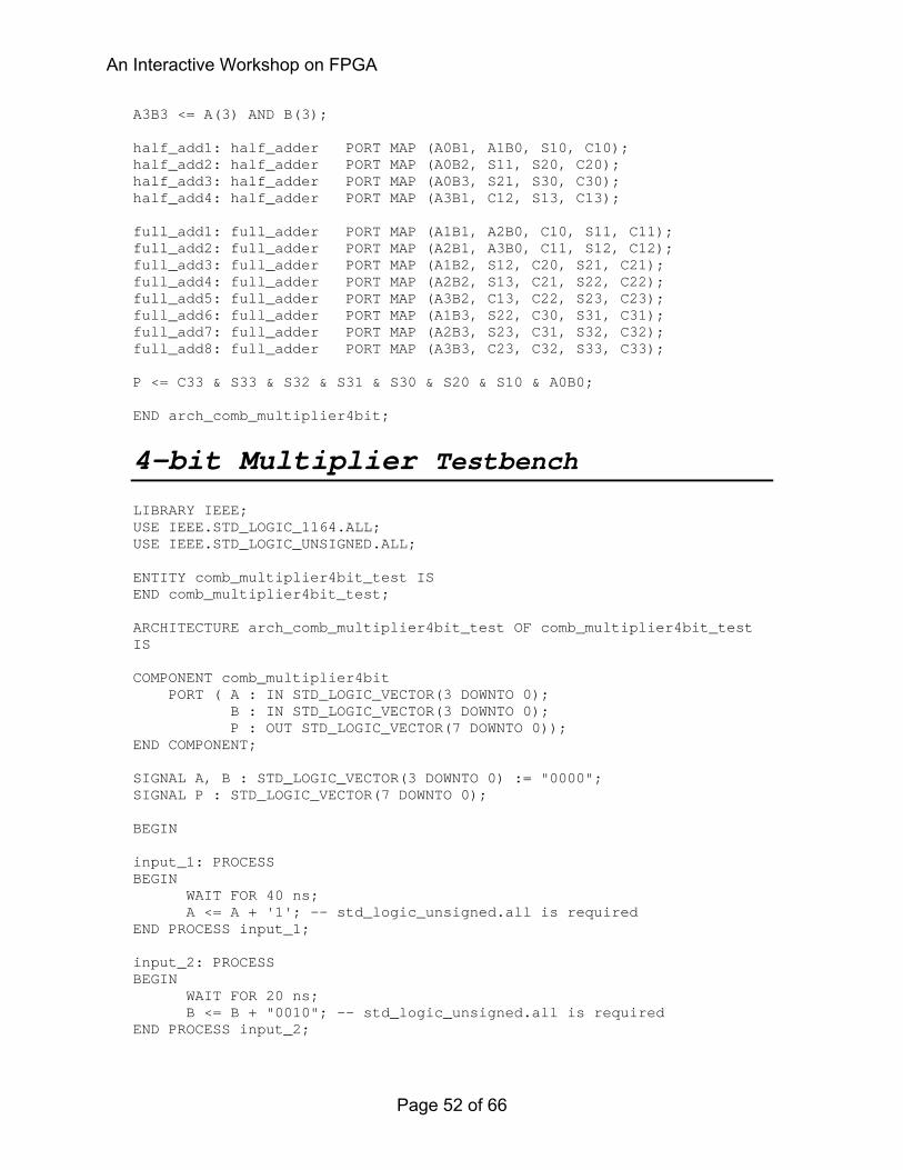
A3B3 <= A(3) AND B(3); half_add1: half_adder PORT MAP (A0B1, A1B0, S10, C10); half_add2: half_adder PORT MAP (A0B2, S11, S20, C20); half_add3: half_adder PORT MAP (A0B3, S21, S30, C30); half_add4: half_adder PORT MAP (A3B1, C12, S13, C13); full_add1: full_adder PORT MAP (A1B1, A2B0, C10, S11, C11); full_add2: full_adder PORT MAP (A2B1, A3B0, C11, S12, C12); full_add3: full_adder PORT MAP (A1B2, S12, C20, S21, C21); full_add4: full_adder PORT MAP (A2B2, S13, C21, S22, C22); full_add5: full_adder PORT MAP (A3B2, C13, C22, S23, C23); full_add6: full_adder PORT MAP (A1B3, S22, C30, S31, C31); full_add7: full_adder PORT MAP (A2B3, S23, C31, S32, C32); full_add8: full_adder PORT MAP (A3B3, C23, C32, S33, C33); P <= C33 & S33 & S32 & S31 & S30 & S20 & S10 & A0B0; END arch_comb_multiplier4bit; 4-bit Multiplier Testbench LIBRARY IEEE; USE IEEE.STD_LOGIC_1164.ALL; USE IEEE.STD_LOGIC_UNSIGNED.ALL; ENTITY comb_multiplier4bit_test IS END comb_multiplier4bit_test; ARCHITECTURE arch_comb_multiplier4bit_test OF comb_multiplier4bit_test IS COMPONENT comb_multiplier4bit PORT ( A : IN STD_LOGIC_VECTOR(3 DOWNTO 0); B : IN STD_LOGIC_VECTOR(3 DOWNTO 0); P : OUT STD_LOGIC_VECTOR(7 DOWNTO 0)); END COMPONENT; SIGNAL A, B : STD_LOGIC_VECTOR(3 DOWNTO 0) := "0000"; SIGNAL P : STD_LOGIC_VECTOR(7 DOWNTO 0); BEGIN input_1: PROCESS BEGIN WAIT FOR 40 ns; A <= A + '1'; -- std_logic_unsigned.all is required END PROCESS input_1; input_2: PROCESS BEGIN WAIT FOR 20 ns; B <= B + "0010"; -- std_logic_unsigned.all is required END PROCESS input_2;
An Interactive Workshop on FPGA
Page 52 of 66
comb_mul1: comb_multiplier4bit PORT MAP (A, B, P); END arch_comb_multiplier4bit_test;
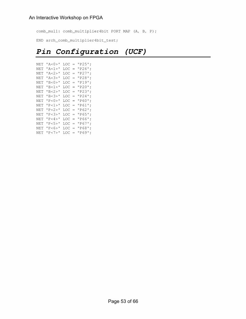
Pin Configuration (UCF) NET "A<0>" LOC = "P25"; NET "A<1>" LOC = "P26"; NET "A<2>" LOC = "P27"; NET "A<3>" LOC = "P28"; NET "B<0>" LOC = "P19"; NET "B<1>" LOC = "P20"; NET "B<2>" LOC = "P23"; NET "B<3>" LOC = "P24"; NET "P<0>" LOC = "P60"; NET "P<1>" LOC = "P61"; NET "P<2>" LOC = "P62"; NET "P<3>" LOC = "P65"; NET "P<4>" LOC = "P66"; NET "P<5>" LOC = "P67"; NET "P<6>" LOC = "P68"; NET "P<7>" LOC = "P69";
An Interactive Workshop on FPGA
Page 53 of 66
LAB # 04 In this lab, we will design sequential circuits in VHDL using the Xilinx 4.1. You will use a typical HDL flow, write the HDL code, and run a functional HDL simulation (Modelsim is integrated with the Xilinx for simulation purpose). After simulation, you will synthesize the HDL code and implement it on Spartan-I FPGA. • 4-bit Sequential Multiplier • 8-bit Binary to BCD Converter (Combinational) • 4-bit Counter with 7-Segment Display After completing this lab, you will be able to: • Perform the basic design flow for writing VHDL code for an iterative algorithm. • Perform the design flow for a circuit having combinational and sequential blocks. • Synthesize the VHDL code, and implement it on FPGA.
An Interactive Workshop on FPGA
Page 54 of 66

4-bit Multiplier (Sequential) LIBRARY IEEE; USE IEEE.STD_LOGIC_1164.ALL; USE IEEE.STD_LOGIC_ARITH.ALL; USE IEEE.STD_LOGIC_UNSIGNED.ALL; ENTITY Booth_Multiplier4bit IS PORT ( multiplier : IN STD_LOGIC_VECTOR(3 DOWNTO 0); multiplicand : IN STD_LOGIC_VECTOR(3 DOWNTO 0); clk : IN STD_LOGIC; rst : IN STD_LOGIC; product : OUT STD_LOGIC_VECTOR(7 DOWNTO 0); valid_out : OUT STD_LOGIC); END Booth_Multiplier4bit; ARCHITECTURE arch_Booth_Multiplier4bit OF Booth_Multiplier4bit IS SIGNAL M,Q,A : std_logic_vector(3 DOWNTO 0); SIGNAL C : std_logic; SIGNAL t5bits_1 : std_logic_vector(4 DOWNTO 0); SIGNAL Q2 : std_logic_vector(3 DOWNTO 0); BEGIN PROCESS(clk,rst) VARIABLE state : integer; VARIABLE count : integer; BEGIN IF rst='1' THEN M <= "0000"; Q <= "0000"; Q2 <= "0000"; A <= "0000"; count := 4; C <= '0'; valid_out <= '0'; state := 0; t5bits_1 <= "00000"; ELSIF clk='1' AND clk'EVENT THEN CASE state IS WHEN 0 => state := state + 1; M <= multiplicand; Q <= multiplier; Q2 <= multiplier; t5bits_1 <= "00000"; C <= '0'; A <= "0000"; valid_out <= '0'; count := 4; WHEN 1 => IF Q(0)='1' THEN state := 2;
An Interactive Workshop on FPGA
Page 55 of 66
t5bits_1 <= ('0' & A)+('0' & M); ELSE state := 3; END IF; WHEN 2 => state := 3; C <= t5bits_1(4); A <= t5bits_1(3 DOWNTO 0); WHEN 3 => state := state + 1; FOR i IN 0 to 2 LOOP Q(i) <= Q(i+1); END LOOP; Q(3) <= A(0); FOR i IN 0 to 2 LOOP A(i) <= A(i+1); END LOOP; A(3) <= C; C <= '0'; count := count - 1; WHEN 4 => IF count=0 THEN state := state + 1; valid_out <= '1'; ELSE state := 1; END IF; WHEN 5 => IF(M=multiplicand) THEN IF(Q2=multiplier) THEN state := 5; valid_out <= '1'; ELSE state := 0; valid_out <= '0'; END IF; ELSE state := 0; valid_out <= '0'; END IF; WHEN OTHERS => state := 0; END CASE; END IF; END PROCESS; Product <= A & Q; END arch_Booth_Multiplier4bit;
4-bit Multiplier Testbench LIBRARY IEEE; USE IEEE.STD_LOGIC_1164.ALL; USE IEEE.STD_LOGIC_UNSIGNED.ALL; ENTITY Booth_Multiplier4bit_test IS END Booth_Multiplier4bit_test;
An Interactive Workshop on FPGA
Page 56 of 66
ARCHITECTURE arch_Booth_Multiplier4bit_test OF Booth_Multiplier4bit_test IS COMPONENT Booth_Multiplier4bit PORT ( multiplier : IN STD_LOGIC_VECTOR(3 DOWNTO 0); multiplicand : IN STD_LOGIC_VECTOR(3 DOWNTO 0); clk : IN STD_LOGIC; rst : IN STD_LOGIC; product : OUT STD_LOGIC_VECTOR(7 DOWNTO 0); valid_out : OUT STD_LOGIC); END COMPONENT; SIGNAL multiplier, multiplicand : STD_LOGIC_VECTOR(3 DOWNTO 0) := "0000"; SIGNAL clk, rst : STD_LOGIC := '0'; SIGNAL product : STD_LOGIC_VECTOR(7 DOWNTO 0); SIGNAL valid_out : STD_LOGIC; BEGIN input_1: PROCESS BEGIN -- WAIT FOR 600 ns; WAIT UNTIL valid_out='1'; multiplier <= multiplier + '1'; -- std_logic_unsigned.all is required END PROCESS input_1; input_2: PROCESS BEGIN -- WAIT FOR 600 ns; WAIT UNTIL valid_out='1'; multiplicand <= multiplicand + "0010"; -- std_logic_unsigned.all is required END PROCESS input_2; clk_gen: PROCESS BEGIN LOOP WAIT FOR 20 ns; clk <= NOT clk; END LOOP; END PROCESS clk_gen; rst_gen: PROCESS BEGIN rst <= '1'; WAIT FOR 30 ns; rst <= '0'; WAIT; END PROCESS rst_gen; Booth_Mul1: Booth_Multiplier4bit PORT MAP (multiplier, multiplicand, clk, rst, product, valid_out);
An Interactive Workshop on FPGA
Page 57 of 66
END arch_Booth_Multiplier4bit_test;
Pin Configuration (UCF) NET "multiplier<0>" LOC = "P25"; NET "multiplier<1>" LOC = "P26"; NET "multiplier<2>" LOC = "P27"; NET "multiplier<3>" LOC = "P28"; NET "multiplicand<0>" LOC = "P19"; NET "multiplicand<1>" LOC = "P20"; NET "multiplicand<2>" LOC = "P23"; NET "multiplicand<3>" LOC = "P24"; NET "product<0>" LOC = "P60"; NET "product<1>" LOC = "P61"; NET "product<2>" LOC = "P62"; NET "product<3>" LOC = "P65"; NET "product<4>" LOC = "P66"; NET "product<5>" LOC = "P67"; NET "product<6>" LOC = "P68"; NET "product<7>" LOC = "P69"; NET "clk" LOC = "P13"; NET "rst" LOC = "P59"; NET "valid_out" LOC = "P51";
An Interactive Workshop on FPGA
Page 58 of 66

8-bit Binary to BCD Converter LIBRARY IEEE; USE IEEE.STD_LOGIC_1164.ALL; USE IEEE.STD_LOGIC_UNSIGNED.ALL; ENTITY binary_BCD_converter IS PORT(binary: IN std_logic_vector(7 DOWNTO 0); unit_out,ten_out: OUT std_logic_vector(3 DOWNTO 0); hundred_out: OUT std_logic_vector(1 DOWNTO 0)); END binary_BCD_converter; ARCHITECTURE arch_binary_BCD_converter OF binary_BCD_converter IS COMPONENT add3 PORT(binary_in: IN std_logic_vector(3 DOWNTO 0); BCD_out: OUT std_logic_vector(3 DOWNTO 0)); END COMPONENT; SIGNAL add_in1,add_in2,add_in3,add_in4,add_in5, add_in6,add_in7:std_logic_vector(3 DOWNTO 0); SIGNAL add_out1,add_out2,add_out3,add_out4,add_out5, add_out6,add_out7:std_logic_vector(3 DOWNTO 0); BEGIN c1: add3 PORT MAP (add_in1,add_out1); c2: add3 PORT MAP (add_in2,add_out2); c3: add3 PORT MAP (add_in3,add_out3); c4: add3 PORT MAP (add_in4,add_out4); c5: add3 PORT MAP (add_in5,add_out5); c6: add3 PORT MAP (add_in6,add_out6); c7: add3 PORT MAP (add_in7,add_out7); add_in1 <= '0' & binary(7 DOWNTO 5); add_in2 <= add_out1(2 DOWNTO 0) & binary(4); add_in3 <= add_out2(2 DOWNTO 0) & binary(3); add_in4 <= add_out3(2 DOWNTO 0) & binary(2); add_in5 <= add_out4(2 DOWNTO 0) & binary(1); add_in6 <= '0' & add_out1(3) & add_out2(3) & add_out3(3); add_in7 <= add_out6(2 DOWNTO 0) & add_out4(3); unit_out <= add_out5(2 DOWNTO 0) & binary(0); ten_out <= add_out7(2 DOWNTO 0) & add_out5(3); hundred_out <= add_out6(3) & add_out7(3); END arch_binary_BCD_converter; LIBRARY IEEE; USE IEEE.STD_LOGIC_1164.ALL; USE IEEE.STD_LOGIC_UNSIGNED.ALL; ENTITY add3 IS PORT(binary_in: IN std_logic_vector(3 DOWNTO 0);
An Interactive Workshop on FPGA
Page 59 of 66
BCD_out: OUT std_logic_vector(3 DOWNTO 0)); END add3; ARCHITECTURE arch_add3 OF add3 IS BEGIN PROCESS(binary_in) BEGIN CASE binary_in IS WHEN "0000" => BCD_out <= "0000"; WHEN "0001" => BCD_out <= "0001"; WHEN "0010" => BCD_out <= "0010"; WHEN "0011" => BCD_out <= "0011"; WHEN "0100" => BCD_out <= "0100"; WHEN "0101" => BCD_out <= "1000"; WHEN "0110" => BCD_out <= "1001"; WHEN "0111" => BCD_out <= "1010"; WHEN "1000" => BCD_out <= "1011"; WHEN "1001" => BCD_out <= "1100"; WHEN OTHERS => BCD_out <= "0000"; END CASE; END PROCESS; END arch_add3;
8-bit Binary to BCD Converter Testbench LIBRARY IEEE; USE IEEE.STD_LOGIC_1164.ALL; USE IEEE.STD_LOGIC_UNSIGNED.ALL; ENTITY binary_BCD_converter_test IS END binary_BCD_converter_test; ARCHITECTURE arch_binary_BCD_converter_test OF binary_BCD_converter_test IS COMPONENT binary_BCD_converter PORT(binary: IN std_logic_vector(7 DOWNTO 0); unit_out,ten_out: OUT std_logic_vector(3 DOWNTO 0); hundred_out: OUT std_logic_vector(1 DOWNTO 0)); END COMPONENT; SIGNAL binary : STD_LOGIC_VECTOR(7 DOWNTO 0) := (OTHERS=>'0'); SIGNAL unit_out, ten_out : STD_LOGIC_VECTOR(3 DOWNTO 0); SIGNAL hundred_out : STD_LOGIC_VECTOR(1 DOWNTO 0); BEGIN input: PROCESS BEGIN WAIT FOR 20 ns; binary <= binary + '1'; -- std_logic_unsigned.all is required END PROCESS input;
An Interactive Workshop on FPGA
Page 60 of 66
bin_BCD1: binary_BCD_converter PORT MAP (binary, unit_out, ten_out, hundred_out); END arch_binary_BCD_converter_test;
Pin Configuration (UCF) NET "binary<0>" LOC = "P19"; NET "binary<1>" LOC = "P20"; NET "binary<2>" LOC = "P23"; NET "binary<3>" LOC = "P24"; NET "binary<4>" LOC = "P25"; NET "binary<5>" LOC = "P26"; NET "binary<6>" LOC = "P27"; NET "binary<7>" LOC = "P28"; NET "unit_out<0>" LOC = "P60"; NET "unit_out<1>" LOC = "P61"; NET "unit_out<2>" LOC = "P62"; NET "unit_out<3>" LOC = "P65"; NET "ten_out<0>" LOC = "P66"; NET "ten_out<1>" LOC = "P67"; NET "ten_out<2>" LOC = "P68"; NET "ten_out<3>" LOC = "P69"; NET "hundred_out<0>" LOC = "P50"; NET "hundred_out<1>" LOC = "P46";
An Interactive Workshop on FPGA
Page 61 of 66
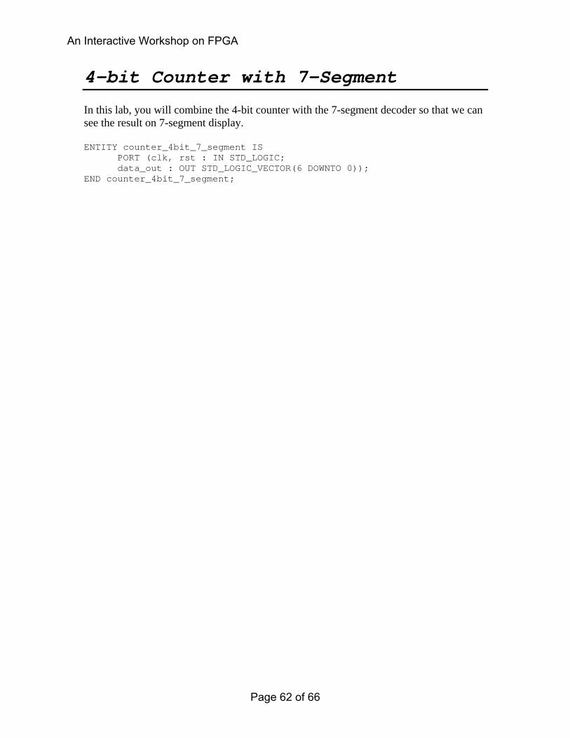
4-bit Counter with 7-Segment In this lab, you will combine the 4-bit counter with the 7-segment decoder so that we can see the result on 7-segment display. ENTITY counter_4bit_7_segment IS PORT (clk, rst : IN STD_LOGIC; data_out : OUT STD_LOGIC_VECTOR(6 DOWNTO 0)); END counter_4bit_7_segment;
An Interactive Workshop on FPGA
Page 62 of 66

LAB # 05 In this lab, we will design a circuit of Ripple Carry Adder and Multiplier. At one time only one operation can be performed and user can select the desired operation. The output of the addition will be displayed on 7-segment display in hexadecimal format (carry out will be discarded). The output of the multiplier will be displayed on 7-segment in BCD format. The block diagram of the circuit, and pin configuration is given, and you will write the VHDL code yourself using whatever style you like. Some of the blocks in this design have been implemented in previous labs, so it would be wise to use those blocks wherever possible. Note: To make the debugging easier, use the same wire names as given in block diagram. After completing this lab, you will be able to: • Write the synthesizable VHDL code for any given block diagram.
An Interactive Workshop on FPGA
Page 63 of 66
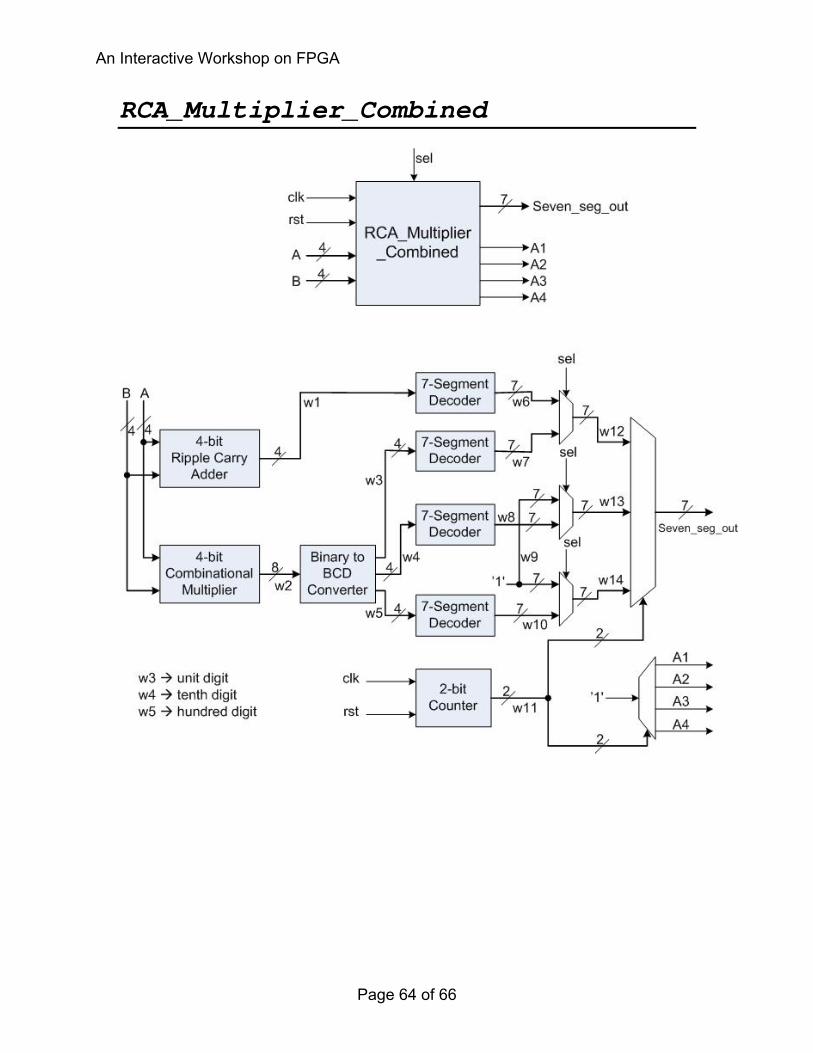
RCA_Multiplier_Combined
An Interactive Workshop on FPGA
Page 64 of 66
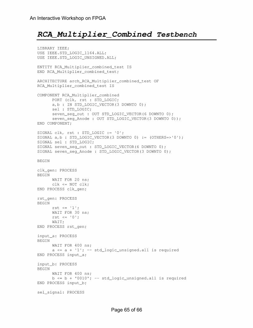
RCA_Multiplier_Combined Testbench LIBRARY IEEE; USE IEEE.STD_LOGIC_1164.ALL; USE IEEE.STD_LOGIC_UNSIGNED.ALL; ENTITY RCA_Multiplier_combined_test IS END RCA_Multiplier_combined_test; ARCHITECTURE arch_RCA_Multiplier_combined_test OF RCA_Multiplier_combined_test IS COMPONENT RCA_Multiplier_combined PORT (clk, rst : STD_LOGIC; a,b : IN STD_LOGIC_VECTOR(3 DOWNTO 0); sel : STD_LOGIC; seven_seg_out : OUT STD_LOGIC_VECTOR(6 DOWNTO 0); seven_seg_Anode : OUT STD_LOGIC_VECTOR(3 DOWNTO 0)); END COMPONENT; SIGNAL clk, rst : STD_LOGIC := '0'; SIGNAL a,b : STD_LOGIC_VECTOR(3 DOWNTO 0) := (OTHERS=>'0'); SIGNAL sel : STD_LOGIC; SIGNAL seven_seg_out : STD_LOGIC_VECTOR(6 DOWNTO 0); SIGNAL seven_seg_Anode : STD_LOGIC_VECTOR(3 DOWNTO 0); BEGIN clk_gen: PROCESS BEGIN WAIT FOR 20 ns; clk <= NOT clk; END PROCESS clk_gen; rst_gen: PROCESS BEGIN rst <= '1'; WAIT FOR 30 ns; rst <= '0'; WAIT; END PROCESS rst_gen; input_a: PROCESS BEGIN WAIT FOR 400 ns; a <= a + '1'; -- std_logic_unsigned.all is required END PROCESS input_a; input_b: PROCESS BEGIN WAIT FOR 400 ns; b <= b + "0010"; -- std_logic_unsigned.all is required END PROCESS input_b; sel_signal: PROCESS
An Interactive Workshop on FPGA
Page 65 of 66
BEGIN sel <= '0'; WAIT FOR 2000 ns; sel <= '1'; WAIT FOR 2000 ns; END PROCESS sel_signal; RCA_mult: RCA_Multiplier_combined PORT MAP(clk, rst, a, b, sel, seven_seg_out, seven_seg_Anode); END arch_RCA_Multiplier_combined_test;
Pin Configuration (UCF) NET "a<0>" LOC = "P25"; NET "a<1>" LOC = "P26"; NET "a<2>" LOC = "P27"; NET "a<3>" LOC = "P28"; NET "b<0>" LOC = "P19"; NET "b<1>" LOC = "P20"; NET "b<2>" LOC = "P23"; NET "b<3>" LOC = "P24"; NET "clk" LOC = "P13"; NET "rst" LOC = "P59"; NET "sel" LOC = "P58"; NET "seven_seg_Anode<0>" LOC = "P44"; NET "seven_seg_Anode<1>" LOC = "P40"; NET "seven_seg_Anode<2>" LOC = "P39"; NET "seven_seg_Anode<3>" LOC = "P38"; NET "seven_seg_out<0>" LOC = "P45"; NET "seven_seg_out<1>" LOC = "P46"; NET "seven_seg_out<2>" LOC = "P47"; NET "seven_seg_out<3>" LOC = "P48"; NET "seven_seg_out<4>" LOC = "P49"; NET "seven_seg_out<5>" LOC = "P50"; NET "seven_seg_out<6>" LOC = "P51";
An Interactive Workshop on FPGA
Page 66 of 66
Copyright Digilent, Inc. All rights reserved Document: 502-002
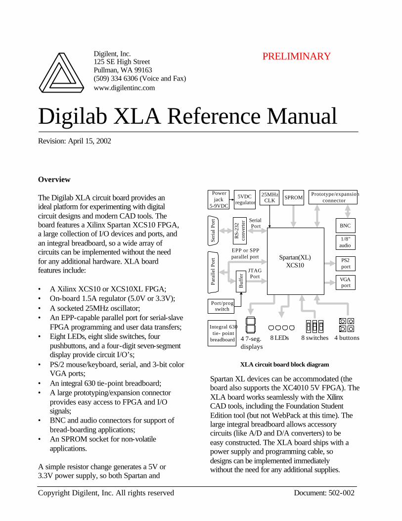
Digilab XLA Reference Manual Revision: April 15, 2002 Overview The Digilab XLA circuit board provides an ideal platform for experimenting with digital circuit designs and modern CAD tools. The board features a Xilinx Spartan XCS10 FPGA, a large collection of I/O devices and ports, and an integral breadboard, so a wide array of circuits can be implemented without the need for any additional hardware. XLA board features include: • A Xilinx XCS10 or XCS10XL FPGA; • On-board 1.5A regulator (5.0V or 3.3V); • A socketed 25MHz oscillator; • An EPP-capable parallel port for serial-slave
FPGA programming and user data transfers; • Eight LEDs, eight slide switches, four
pushbuttons, and a four-digit seven-segment display provide circuit I/O’s;
• PS/2 mouse/keyboard, serial, and 3-bit color VGA ports;
• An integral 630 tie-point breadboard; • A large prototyping/expansion connector
provides easy access to FPGA and I/O signals;
• BNC and audio connectors for support of bread-boarding applications;
• An SPROM socket for non-volatile applications.
A simple resistor change generates a 5V or 3.3V power supply, so both Spartan and
Spartan XL devices can be accommodated (the board also supports the XC4010 5V FPGA). The XLA board works seamlessly with the Xilinx CAD tools, including the Foundation Student Edition tool (but not WebPack at this time). The large integral breadboard allows accessory circuits (like A/D and D/A converters) to be easy constructed. The XLA board ships with a power supply and programming cable, so designs can be implemented immediately without the need for any additional supplies.
Digilent, Inc. 125 SE High Street Pullman, WA 99163 (509) 334 6306 (Voice and Fax) www.digilentinc.com
5VDC
regulator
8 LEDs4 7-seg.displays
8 switches 4 buttons
PS2port
VGAport
Powerjack
5-9VDCSe
rial
Por
tPa
ralle
l Por
t
Port/prog switch
EPP or SPPparallel port
JTAGPort
SerialPort
Buf
fer
RS-
232
conv
erte
r
Prototype/expansionconnector
Integral 630tie- point
breadboard
BNC
1/8"audio
25MHzCLK SPROM
Spartan(XL)XCS10
XLA circuit board block diagram
PRELIMINARY

Copyright Digilent, Inc. Digilab XLA Reference Manual 2/12
Rev: Apr 15, 2002 www.digilentinc.com Page 2 of 12
Functional Description The XLA board provides a self-contained digital circuit design environment that offers an ideal platform for experimenting with digital circuit designs and/or modern CAD tools. A large-capacity gate array, provide allow a wide array of designs to be implemented without the need for any additional hardware. Signals The Digilab board has been designed to allow rapid circuit construction and convenient test lead attachment. Most signals are routed to the prototyping connector (J1), to the gate array, and to a test lead connector. Depending on function, the signals arise from devices or connectors on the board, or they drive devices or connectors on the board. The table defines all Digilab signals and shows all their connections. Circuit board The FR-4 fiberglass circuit board uses a 1oz. copper, two layer, plated through-hole process with 6mil minimum trace size and .039” through-holes. Solder mask is provided on both sides, a silk-screen is provided on the component side, and all connectors can accommodate mechanical stays. Four 6/32”-sized corner holes are provided for stand-offs (to keep the board from contacting the work surface).
Power Supply The circuits and components on the Digilab XL board require a 5VDC or 3.3VDC power supply. The board is equipped with a LM317T
Signal Definition Connections
A1 - A4 Seven-segment Anodes SSDs, FPGA, J1 CA - CG Seven-segment Cathodes SSDs, FPGA, J1 DP Seven-segment Decimal Point SSDs, J1 BTN1 - 4 Push Button connections Buttons, FPGA, J1 SW1 - SW8 Slide switch connections Switches, FPGA, J1 LD1 - LD8 LED connections LEDs, FPGA, J1 LDG Gate connection on 74HC373 74HC373, FPGA, J1 ASFT Audio connector shaft Audio connector, J1 ATIP Audio connector tip Audio connector, J1 CLK1 CLK1 connected to PGCK1 CLK1, FPGA CLK2 CLK2 connected to PGCK2 CLK2, FPGA, J1 O1 - O5 Unassigned FPGA pins FPGA, J1, J2 PD0 - PD7 Parallel port data pins J7 (par. port), FPGA, J1, J3 PWE Parallel port Write Enable (EPP) J7 (par. port), FPGA, J1, J3 PAS Parallel port Address Strobe (EPP) J7 (par. port), FPGA, J1, J3 PDS Parallel port Data Strobe (EPP) J7 (par. port), FPGA, J1, J3 PINT Parallel port Interrupt (EPP) J7 (par. port), FPGA, J1, J3 PRS Parallel port Reset (EPP) J7 (par. port), FPGA, J1, J3 PWT Parallel port Wait/Busy (EPP) J7 (par. port), FPGA, J3 BNCS BNC connector shield BNC connector, J1 BNCP BNC connector center post BNC connector, J1 R, G, B VGA Red, Green, and Blue signals J6 (vga), FPGA, J2 HS VGA Horizontal Sync J6 (vga), FPGA, J2 VS VGA Vertical Sync J6 (vga), FPGA, J2 RXD, TXD RS-232 receive and send signals J4 (serial), FPGA, J2 PS2D, PS2C PS2 port data and clock signals J5 (PS/2), FPGA, J1, J2
VinVout
AdjJ8 Powerconnector
Vdd
LD9C2310uF
GND
C241.5uF
R6750
R5240
R4240
U6LM317T
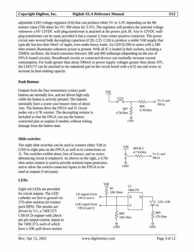
Copyright Digilent, Inc. Digilab XLA Reference Manual 3/12
Rev: Apr 15, 2002 www.digilentinc.com Page 3 of 12
adjustable LDO voltage regulator (U6) that can produce either 5V or 3.3V depending on the R6 resistor value (750 ohms for 5V; 390 ohms for 3.3V). The regulator will produce the selected voltage whenever a 6V-12VDC wall-plug transformer is attached at the power jack J8. Any 6-12VDC wall-plug transformer can be used, provided it has a coaxial 2.1mm center positive connector. The power circuit uses several bulk decoupling capacitors (C20, C23, C24) to produce a stable Vdd supply that typically has less than 50mV of ripple, even under heavy loads. An LED (LD9) in series with a 240-ohm resistor illuminates whenever power is present. With all IC’s loaded in their sockets, including a 25MHz oscillator, the board consumes between 300 and 400 milliamps (depending on the size of FPGA-based circuits). Breadboard circuits or connected devices can markedly increase current consumption. For loads greater than about 500mA or power supply voltages greater than about 10V, the LM317T can be attached to the metalized pad on the circuit board with a 6/32 nut and screw to increase its heat-sinking capacity.
Push Buttons Outputs from the four momentary-contact push buttons are normally low, and are driven high only while the button is actively pressed. The buttons nominally have a worst-case bounce time of about 1ms. The buttons drive the FPGA and J1 circuit nodes via a 4.7K resistor. The decoupling resistor is included so that the FPGA can use the button-connected pins as outputs if needed, without risking damage from the button state. Slide switches
The eight slide switches can be used to connect either Vdd or GND to eight pins on the FPGA as well as to connections on J1. The switches exhibit about 2ms of bounce, and no active debouncing circuit is employed. As shown on the right, a 4.7K-ohm series resistor is used to provide nominal input protection, and to allow the switch-connected inputs to the FPGA to be used as outputs if necessary. LEDs Eight red LEDs are provided for circuit outputs. The LED cathodes are tied to ground via 270-ohm resistors (in resistor pack RP9). The anodes are driven by U1, a 74HC373 CMOS D-register with 24mA per pin output current. Inputs to the 74HC373, each of which have a 10K pull-down resistor
Vdd
GND
RP64.7KOhmRP7
4.7KOhm
To J1 andFPGA
GND
Vdd
To J1 andFPGA
RP4 & 54.7 KOhm
U174HC373
LD signals FromFPGA and J1
GNDGND
LD1- LD8
RP9270 Ohm
RP810K Ohm
D Q
GLDG signal FromFPGA and J1
R110K Ohms
Vdd
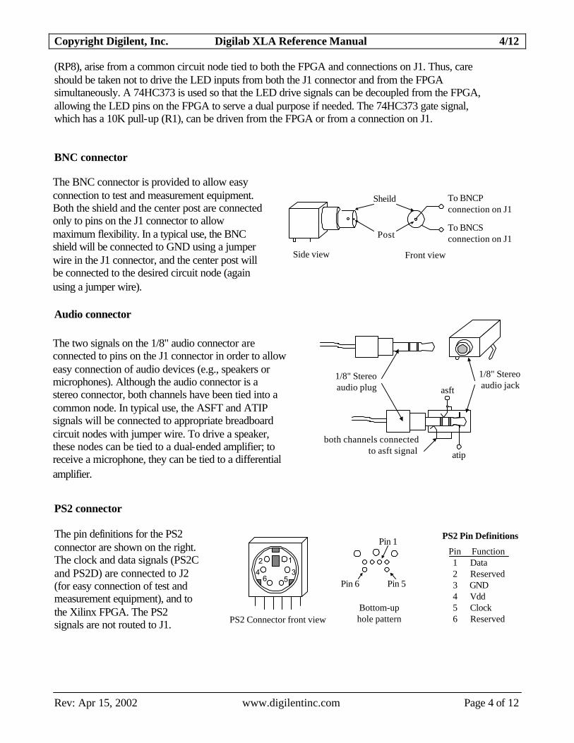
Copyright Digilent, Inc. Digilab XLA Reference Manual 4/12
Rev: Apr 15, 2002 www.digilentinc.com Page 4 of 12
(RP8), arise from a common circuit node tied to both the FPGA and connections on J1. Thus, care should be taken not to drive the LED inputs from both the J1 connector and from the FPGA simultaneously. A 74HC373 is used so that the LED drive signals can be decoupled from the FPGA, allowing the LED pins on the FPGA to serve a dual purpose if needed. The 74HC373 gate signal, which has a 10K pull-up (R1), can be driven from the FPGA or from a connection on J1. BNC connector
Audio connector PS2 connector The pin definitions for the PS2 connector are shown on the right. The clock and data signals (PS2C and PS2D) are connected to J2 (for easy connection of test and measurement equipment), and to the Xilinx FPGA. The PS2 signals are not routed to J1.
The two signals on the 1/8" audio connector are connected to pins on the J1 connector in order to allow easy connection of audio devices (e.g., speakers or microphones). Although the audio connector is a stereo connector, both channels have been tied into a common node. In typical use, the ASFT and ATIP signals will be connected to appropriate breadboard circuit nodes with jumper wire. To drive a speaker, these nodes can be tied to a dual-ended amplifier; to receive a microphone, they can be tied to a differential amplifier.
The BNC connector is provided to allow easy connection to test and measurement equipment. Both the shield and the center post are connected only to pins on the J1 connector to allow maximum flexibility. In a typical use, the BNC shield will be connected to GND using a jumper wire in the J1 connector, and the center post will be connected to the desired circuit node (again using a jumper wire).
PS2 Connector front view
Pin 1
Pin 5Pin 6
Bottom-uphole pattern
PS2 Pin Definitions
Pin Function 1 Data 2 Reserved 3 GND 4 Vdd 5 Clock 6 Reserved
1
53
24
6
1/8" Stereoaudio jack
1/8" Stereoaudio plug
atip
asft
both channels connectedto asft signal
Sheild
Post
To BNCPconnection on J1
Side view Front view
To BNCSconnection on J1
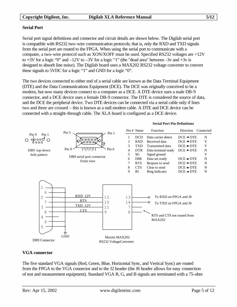
Copyright Digilent, Inc. Digilab XLA Reference Manual 5/12
Rev: Apr 15, 2002 www.digilentinc.com Page 5 of 12
Serial Port Serial port signal definitions and connector and circuit details are shown below. The Digilab serial port is compatible with RS232 two-wire communication protocols; that is, only the RXD and TXD signals from the serial port are routed to the FPGA. When using the serial port to communicate with a computer, a two-wire protocol such as XON/XOFF must be used. Specified RS232 voltages are +12V to +3V for a logic “0” and –12V to –3V for a logic “1” (the "dead area" between -3v and +3v is designed to absorb line noise). The Digilab board uses a MAX202 RS232 voltage converter to convert these signals to 5VDC for a logic “1” and GND for a logic “0”. The two devices connected to either end of a serial cable are known as the Data Terminal Equipment (DTE) and the Data Communications Equipment (DCE). The DCE was originally conceived to be a modem, but now many devices connect to a computer as a DCE. A DTE device uses a male DB-9 connector, and a DCE device uses a female DB-9 connector. The DTE is considered the source of data, and the DCE the peripheral device. Two DTE devices can be connected via a serial cable only if lines two and three are crossed – this is known as a null modem cable. A DTE and DCE device can be connected with a straight-through cable. The XLA board is configured as a DCE device.
DB9 top-downhole pattern
Pin 1
Pin 6Pin 9
Pin 5
DB9 serial port connectorFront view
Pin 1Pin 9
1 62 73 84 95
GND Maxim MAX202RS232 VoltageConverter
RXD_12V
TXD_12V
1210119
131478
To RXD on FPGA and J6
To TXD on FPGA and J6
DB9 Connector
RTS
CTSRTS and CTS not routed fromMAX202
Serial Port Pin Definitions
Pin # Name Function Direction Connected
1 DCD Data carrier detect DCE DTE N 2 RXD Received data DCE DTE Y 3 TXD Transmitted data DCE DTE Y 4 DTR Data terminal ready DCE DTE N 5 SG Signal ground Y 6 DSR Data set ready DCE DTE N 7 RTS Request to send DCE DTE N 8 CTS Clear to send DCE DTE N 9 RI Ring Indicator DCE DTE N
VGA connector The five standard VGA signals (Red, Green, Blue, Horizontal Sync, and Vertical Sync) are routed from the FPGA to the VGA connector and to the J2 header (the J6 header allows for easy connection of test and measurement equipment). Standard VGA R, G, and B signals are terminated with a 75-ohm

Copyright Digilent, Inc. Digilab XLA Reference Manual 6/12
Rev: Apr 15, 2002 www.digilentinc.com Page 6 of 12
pull-down resistor. As shown below, a 470-ohm series resistor drives the R, G, and B signals, and the resistor-divider that is formed ensures the video signals never exceed the VGA-specified maximum of 0.7VDC. Note that each color is either on or off, which allows for eight different colors.
DB15 VGA connectorFront view
Pin 1
Pin 6
Pin 11
Pin 5
Pin 10
Pin 15
Pin 1
Pin 15
DB15 through-hole pattern asseen from the top
1 6 112 7 123 8 134 9 145 10 15
GNDDB15
Connector
To R on FPGA and J2
To G on FPGA and J2
To B on FPGA and J2To HS on FPGA and J2
To VS on FPGA and J2
470 OhmRP11
470 OhmRP11
470 OhmRP11
Parallel Port All parallel port signals except pin 15 (SPP Error), pin 12 (SPP paper out), and pin 13 (SPP Select) are routed. Although the signal names reflect the Enhanced Parallel Port (EPP) mode, any protocol can be used for data transfer. Note that the full ECP protocol (including pin15) can be used if DB25 pin 15 is connected to one of the “open” signals on the FPGA (O1 – O5). All signals are also available at the J3 header for easy test and measurement equipment connection. All signals use 220 ohm series resistors to dampen possible line reflections and decouple the 5VDC port lines from the
Pin EPP signal EPP Function
1 Write Enable (O) Low for read, High for write 2-9 Data bus (B) Bidirectional data lines 10 Interrupt (I) Interrupt/acknowledge input 11 Wait (I) Bus handshake; low to ack 12 Spare NOT CONNECTED 13 Spare NOT CONNECTED 14 Data Strobe (O) Low when data valid 15 Spare NOT CONNECTED 16 Reset (O) Low to reset 17 Address strobe (O) Low when address valid 18-25 GND System ground
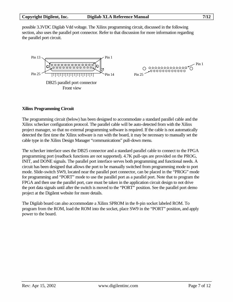
Copyright Digilent, Inc. Digilab XLA Reference Manual 7/12
Rev: Apr 15, 2002 www.digilentinc.com Page 7 of 12
possible 3.3VDC Digilab Vdd voltage. The Xilinx programming circuit, discussed in the following section, also uses the parallel port connector. Refer to that discussion for more information regarding the parallel port circuit.
Xilinx Programming Circuit The programming circuit (below) has been designed to accommodate a standard parallel cable and the Xilinx xchecker configuration protocol. The parallel cable will be auto-detected from with the Xilinx project manager, so that no external programming software is required. If the cable is not automatically detected the first time the Xilinx software is run with the board, it may be necessary to manually set the cable type in the Xilinx Design Manager “communications” pull-down menu. The xchecker interface uses the DB25 connector and a standard parallel cable to connect to the FPGA programming port (readback functions are not supported). 4.7K pull-ups are provided on the PROG, INIT, and DONE signals. The parallel port interface serves both programming and functional needs. A circuit has been designed that allows the port to be manually switched from programming mode to port mode. Slide-switch SW9, located near the parallel port connector, can be placed in the “PROG” mode for programming and “PORT” mode to use the parallel port as a parallel port. Note that to program the FPGA and then use the parallel port, care must be taken in the application circuit design to not drive the port data signals until after the switch is moved to the “PORT” position. See the parallel port demo project at the Digilent website for more details. The Digilab board can also accommodate a Xilinx SPROM in the 8-pin socket labeled ROM. To program from the ROM, load the ROM into the socket, place SW9 in the “PORT” position, and apply power to the board.
Pin 13 Pin 1
Pin 14Pin 25
Pin 1
Pin 25
DB25 parallel port connectorFront view
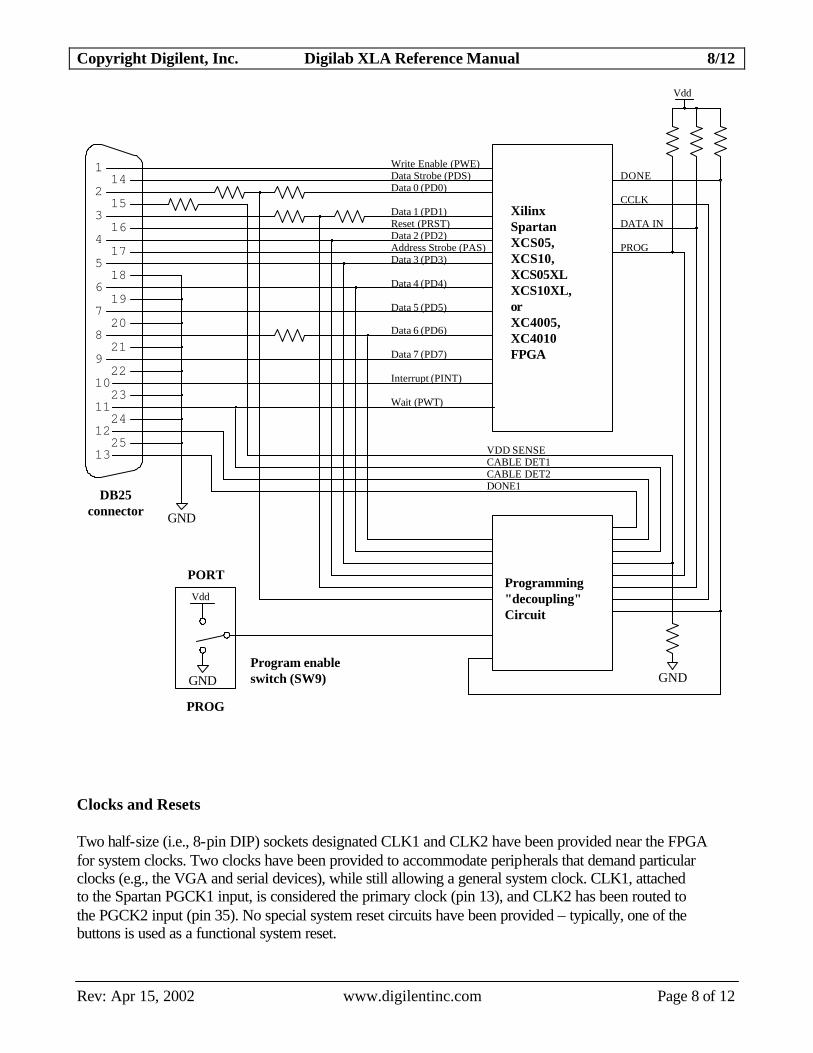
Copyright Digilent, Inc. Digilab XLA Reference Manual 8/12
Rev: Apr 15, 2002 www.digilentinc.com Page 8 of 12
1 142 15316
4 175 18619
720
821
922
1023
1124
1225
13
GND
Data 2 (PD2)
Data 1 (PD1)
Data 0 (PD0)
Data 3 (PD3)
Data 4 (PD4)
Data 5 (PD5)
Data 6 (PD6)
Data 7 (PD7)
Write Enable (PWE)
Interrupt (PINT)
Data Strobe (PDS)
Reset (PRST)
Address Strobe (PAS)
Wait (PWT)
CCLK
DONE
DATA IN
PROG
VDD SENSECABLE DET1
DONE1CABLE DET2
XilinxSpartanXCS05,XCS10,XCS05XLXCS10XL,orXC4005,XC4010FPGA
Programming"decoupling"Circuit
Vdd
GNDGND
Vdd
DB25connector
Program enableswitch (SW9)
PROG
PORT
Clocks and Resets Two half-size (i.e., 8-pin DIP) sockets designated CLK1 and CLK2 have been provided near the FPGA for system clocks. Two clocks have been provided to accommodate peripherals that demand particular clocks (e.g., the VGA and serial devices), while still allowing a general system clock. CLK1, attached to the Spartan PGCK1 input, is considered the primary clock (pin 13), and CLK2 has been routed to the PGCK2 input (pin 35). No special system reset circuits have been provided – typically, one of the buttons is used as a functional system reset.
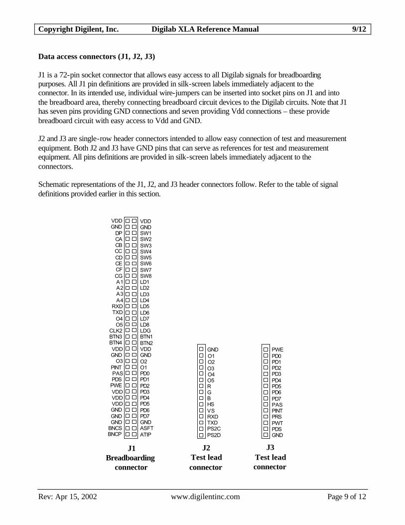
Copyright Digilent, Inc. Digilab XLA Reference Manual 9/12
Rev: Apr 15, 2002 www.digilentinc.com Page 9 of 12
Data access connectors (J1, J2, J3) J1 is a 72-pin socket connector that allows easy access to all Digilab signals for breadboarding purposes. All J1 pin definitions are provided in silk-screen labels immediately adjacent to the connector. In its intended use, individual wire-jumpers can be inserted into socket pins on J1 and into the breadboard area, thereby connecting breadboard circuit devices to the Digilab circuits. Note that J1 has seven pins providing GND connections and seven providing Vdd connections – these provide breadboard circuit with easy access to Vdd and GND. J2 and J3 are single-row header connectors intended to allow easy connection of test and measurement equipment. Both J2 and J3 have GND pins that can serve as references for test and measurement equipment. All pins definitions are provided in silk-screen labels immediately adjacent to the connectors. Schematic representations of the J1, J2, and J3 header connectors follow. Refer to the table of signal definitions provided earlier in this section.
PWEPD0PD1PD2PD3PD4PD5PD6PD7PASPINTPRSPWTPDSGND
VDDGNDSW1SW2SW3SW4SW5SW6SW7SW8LD1LD2LD3LD4LD5LD6LD7LD8LDGBTN1BTN2VDDGNDO2O1PD0PD1PD2PD3PD4PD5PD6PD7GNDASFTATIP
VDDGND
DPCACB
CDCECFCGA1A2A3A4
RXDTXD
O4O5
CLK2BTN3BTN4VDDGND
O3PINTPASPDSPWEVDDVDDVDDGNDGNDGND
BNCSBNCP
CC
J3Test leadconnector
J1Breadboarding
connector
GNDO1O2O3
RGBHSVSRXDTXDPS2CPS2D
O4O5
J2Test leadconnector
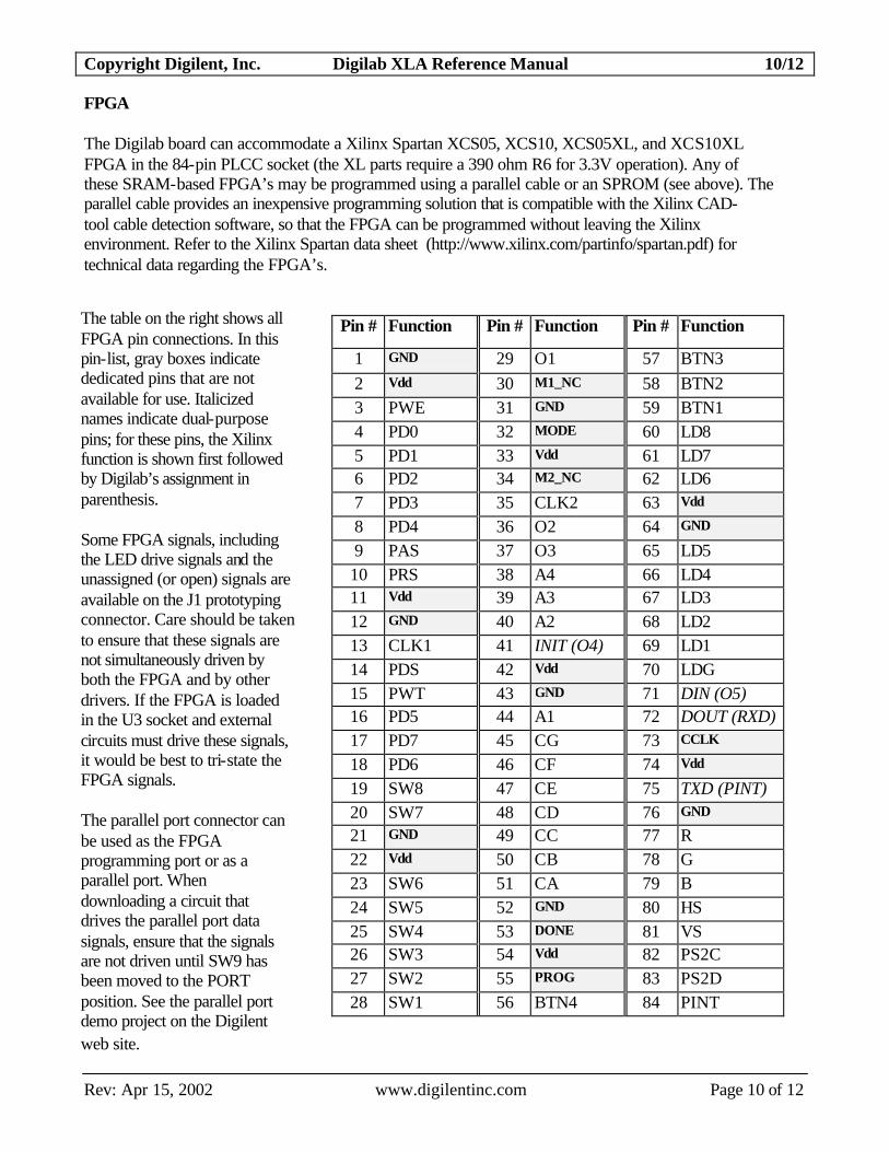
Copyright Digilent, Inc. Digilab XLA Reference Manual 10/12
Rev: Apr 15, 2002 www.digilentinc.com Page 10 of 12
FPGA The Digilab board can accommodate a Xilinx Spartan XCS05, XCS10, XCS05XL, and XCS10XL FPGA in the 84-pin PLCC socket (the XL parts require a 390 ohm R6 for 3.3V operation). Any of these SRAM-based FPGA’s may be programmed using a parallel cable or an SPROM (see above). The parallel cable provides an inexpensive programming solution that is compatible with the Xilinx CAD-tool cable detection software, so that the FPGA can be programmed without leaving the Xilinx environment. Refer to the Xilinx Spartan data sheet (http://www.xilinx.com/partinfo/spartan.pdf) for technical data regarding the FPGA’s.
Pin # Function Pin # Function Pin # Function
1 GND 29 O1 57 BTN3 2 Vdd 30 M1_NC 58 BTN2 3 PWE 31 GND 59 BTN1 4 PD0 32 MODE 60 LD8 5 PD1 33 Vdd 61 LD7 6 PD2 34 M2_NC 62 LD6 7 PD3 35 CLK2 63 Vdd
8 PD4 36 O2 64 GND
9 PAS 37 O3 65 LD5 10 PRS 38 A4 66 LD4 11 Vdd 39 A3 67 LD3 12 GND 40 A2 68 LD2 13 CLK1 41 INIT (O4) 69 LD1 14 PDS 42 Vdd 70 LDG 15 PWT 43 GND 71 DIN (O5)
16 PD5 44 A1 72 DOUT (RXD) 17 PD7 45 CG 73 CCLK
18 PD6 46 CF 74 Vdd
19 SW8 47 CE 75 TXD (PINT) 20 SW7 48 CD 76 GND
21 GND 49 CC 77 R 22 Vdd 50 CB 78 G 23 SW6 51 CA 79 B 24 SW5 52 GND 80 HS 25 SW4 53 DONE 81 VS 26 SW3 54 Vdd 82 PS2C 27 SW2 55 PROG 83 PS2D 28 SW1 56 BTN4 84 PINT
The table on the right shows all FPGA pin connections. In this pin-list, gray boxes indicate dedicated pins that are not available for use. Italicized names indicate dual-purpose pins; for these pins, the Xilinx function is shown first followed by Digilab’s assignment in parenthesis. Some FPGA signals, including the LED drive signals and the unassigned (or open) signals are available on the J1 prototyping connector. Care should be taken to ensure that these signals are not simultaneously driven by both the FPGA and by other drivers. If the FPGA is loaded in the U3 socket and external circuits must drive these signals, it would be best to tri-state the FPGA signals. The parallel port connector can be used as the FPGA programming port or as a parallel port. When downloading a circuit that drives the parallel port data signals, ensure that the signals are not driven until SW9 has been moved to the PORT position. See the parallel port demo project on the Digilent web site.
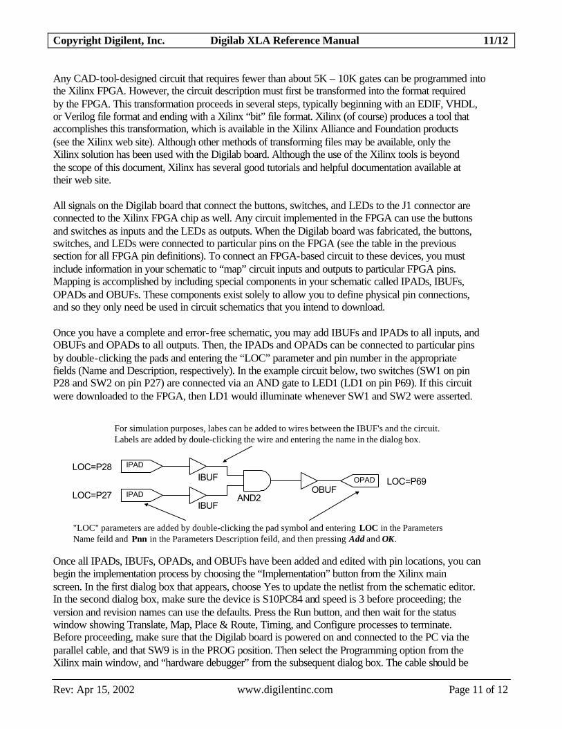
Copyright Digilent, Inc. Digilab XLA Reference Manual 11/12
Rev: Apr 15, 2002 www.digilentinc.com Page 11 of 12
Any CAD-tool-designed circuit that requires fewer than about 5K – 10K gates can be programmed into the Xilinx FPGA. However, the circuit description must first be transformed into the format required by the FPGA. This transformation proceeds in several steps, typically beginning with an EDIF, VHDL, or Verilog file format and ending with a Xilinx “bit” file format. Xilinx (of course) produces a tool that accomplishes this transformation, which is available in the Xilinx Alliance and Foundation products (see the Xilinx web site). Although other methods of transforming files may be available, only the Xilinx solution has been used with the Digilab board. Although the use of the Xilinx tools is beyond the scope of this document, Xilinx has several good tutorials and helpful documentation available at their web site. All signals on the Digilab board that connect the buttons, switches, and LEDs to the J1 connector are connected to the Xilinx FPGA chip as well. Any circuit implemented in the FPGA can use the buttons and switches as inputs and the LEDs as outputs. When the Digilab board was fabricated, the buttons, switches, and LEDs were connected to particular pins on the FPGA (see the table in the previous section for all FPGA pin definitions). To connect an FPGA-based circuit to these devices, you must include information in your schematic to “map” circuit inputs and outputs to particular FPGA pins. Mapping is accomplished by including special components in your schematic called IPADs, IBUFs, OPADs and OBUFs. These components exist solely to allow you to define physical pin connections, and so they only need be used in circuit schematics that you intend to download. Once you have a complete and error-free schematic, you may add IBUFs and IPADs to all inputs, and OBUFs and OPADs to all outputs. Then, the IPADs and OPADs can be connected to particular pins by double-clicking the pads and entering the “LOC” parameter and pin number in the appropriate fields (Name and Description, respectively). In the example circuit below, two switches (SW1 on pin P28 and SW2 on pin P27) are connected via an AND gate to LED1 (LD1 on pin P69). If this circuit were downloaded to the FPGA, then LD1 would illuminate whenever SW1 and SW2 were asserted.
Once all IPADs, IBUFs, OPADs, and OBUFs have been added and edited with pin locations, you can begin the implementation process by choosing the “Implementation” button from the Xilinx main screen. In the first dialog box that appears, choose Yes to update the netlist from the schematic editor. In the second dialog box, make sure the device is S10PC84 and speed is 3 before proceeding; the version and revision names can use the defaults. Press the Run button, and then wait for the status window showing Translate, Map, Place & Route, Timing, and Configure processes to terminate. Before proceeding, make sure that the Digilab board is powered on and connected to the PC via the parallel cable, and that SW9 is in the PROG position. Then select the Programming option from the Xilinx main window, and “hardware debugger” from the subsequent dialog box. The cable should be
AND2
IBUF
IBUF
OBUFOPAD
IPAD
IPAD
LOC=P28
LOC=P27LOC=P69
For simulation purposes, labes can be added to wires between the IBUF's and the circuit.Labels are added by doule-clicking the wire and entering the name in the dialog box.
"LOC" parameters are added by double-clicking the pad symbol and entering LOC in the ParametersName feild and Pnn in the Parameters Description feild, and then pressing Add and OK.
Copyright Digilent, Inc. Digilab XLA Reference Manual 12/12
Rev: Apr 15, 2002 www.digilentinc.com Page 12 of 12
auto-detected; if not, manually choose the parallel cable in the Cable à communications dialog box. Once the cable has been detected, you can download your design simply by double-clicking on the appropriate file name in the hardware debugger window. Two 8-pin DIP clock sockets have been provided for use with the FPGA. Labeled CLK1 and CLK2, they connect to pin 13 (Xilinx primary clock buffer #1) and pin 35 (Xilinx primary clock buffer #2). Clock sources up to 80MHz have been successfully used with the board. The FPGA programming circuit has been designed to accommodate a standard parallel cable or an SPROM. When programming the FPGA from within the Xilinx CAD tool, the parallel cable will be automatically detected (so no external programming software is required). If a cable is not automatically detected the first time the Xilinx software is run with the board, it may be necessary to manually set the cable type in the Xilinx Design Manager “communications” pull-down menu. The parallel port interface serves both programming and functional needs. A circuit has been designed that allows the port to be manually switched from programming mode to port mode. Slide-switch SW9, located near the parallel port connector, must be placed in the “PROG” mode for programming from a host PC and “PORT” mode to use the parallel port as a parallel port or to program from an onboard ROM at power-up. Note that to program the FPGA and then use the parallel port, care must be taken in the application circuit design to not drive the port data signals until after the switch is moved to the “PORT” position.
Recommended