1
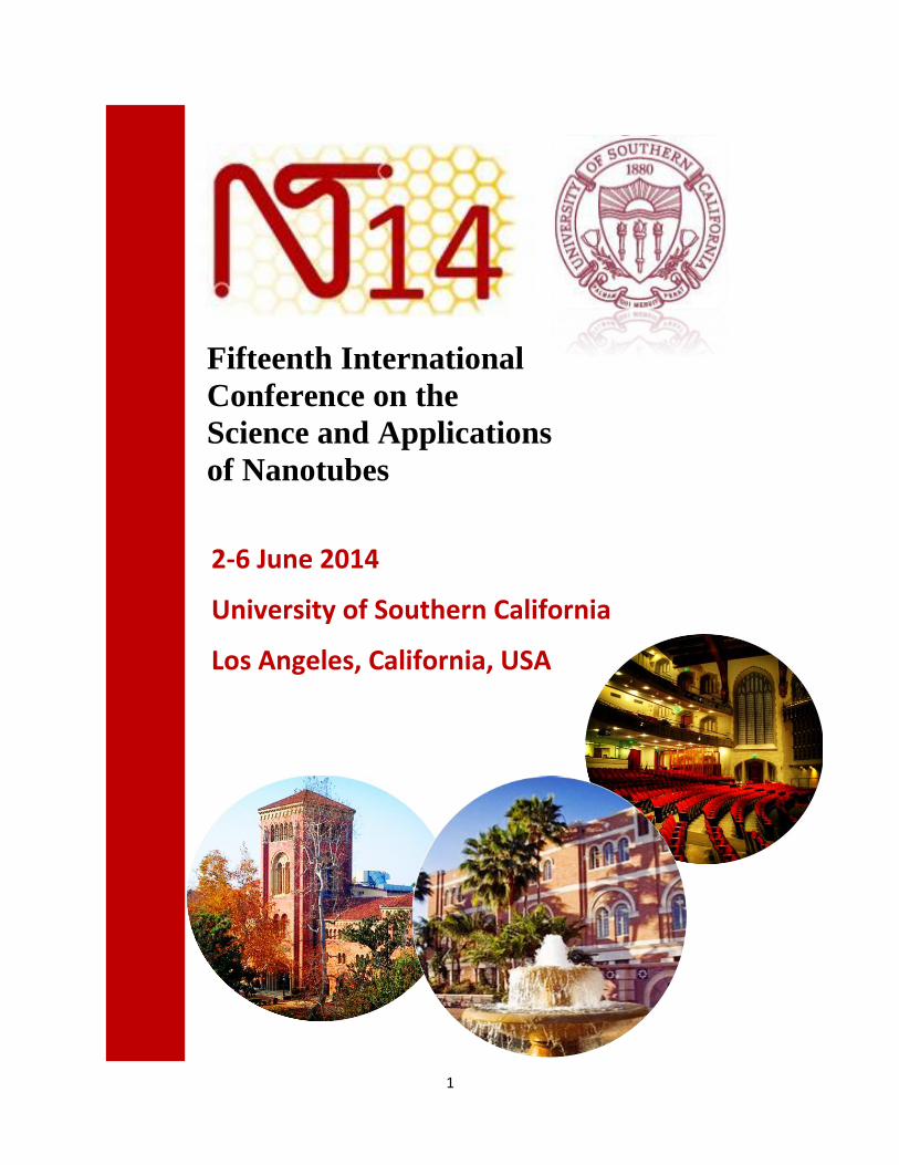
Fifteenth International
Conference on the
Science and Applications
of Nanotubes
2-6 June 2014
University of Southern California
Los Angeles, California, USA

2
Sunday Monday Tuesday Wednesday Thursday Friday Saturday
June 1 June 2 June 3 June 4 June 5 June 6 June 7
9:00
9:15
9:30
9:45 H.Kataura
10:00 Y. Nakai
10:15 R. Saito Artyukhov R. Zhang S.Maruyama M. Picher
10:30 Nasibulin H. Hasdeo Goltapehei R. Krupke Xi Ling
10:45 F. Papadim.
11:00 A. Vierck
11:15 K. Otsuka
11:30 H. Wang
11:45 H. Jiang NT15 Preview
12:00 A. Loiseau Closing
12:15 Lunch
12:30
12:45
13:00
13:15
13:30
13:45
14:00
14:15 O. T. Gul
14:30 S. Cronin
14:45 Nikolaev X. Wei
15:00 J. Campo Sakurai
15:15 J. Yang B. H. Son T.Maruyama
15:30
15:45
16:00
16:15
16:30
16:45
17:00
17:15 G. Soavi T. Susi J. S. Lauret
17:30
17:45
18:00-
20:00
Welcome
Reception
Satellite
Symposia
GSS14
Excursion
and Banquet
Max
Shulaker
Poster
Session 1
and
Exhibition
Poster
Session 3
and
Exhibition
Poster
Session 5
and
Exhibition
Lunch Lunch Lunch
Stephen
PurcellJerry Tersoff
Mikito
Koshino
Alan
Windle
Yuichiro
Kato
Poster
Session 2
and
Exhibition
Summary
and Poster
Shoushan
FanKenji Hata Ming Zheng
Young Hee
Lee
Satellite
Symposia
CCTN14,
MSIN14,
CNTFA14
Poster
Session 4
and
Exhibition
Poster
Session 6
and
Exhibition
Poster 5+6
Summary
Poster 3+4
Summary
Poster 1+2
Summary
Laurent
Cognet
Feng Wang
Florian
Banhart
Alexander
Hoegele
Giorgia
Pastorin
Sofie
Cambre
Yutaka
OhnoR
egi
stra
tio
n/B
adge
Pic
k-u
p
Keynote Talk Poster summary
Invited Talk Poster Session
Contributed Talk Satellite Symposium
NT14 Program Schedule

3
4
5
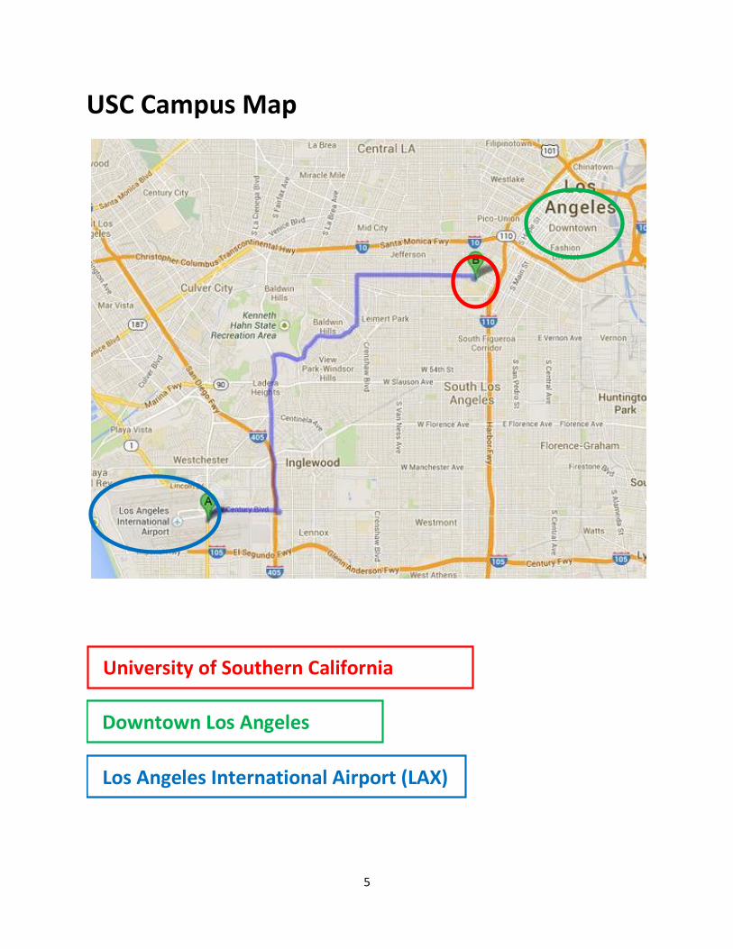
USC Campus Map
University of Southern California
Downtown Los Angeles
Los Angeles International Airport (LAX)
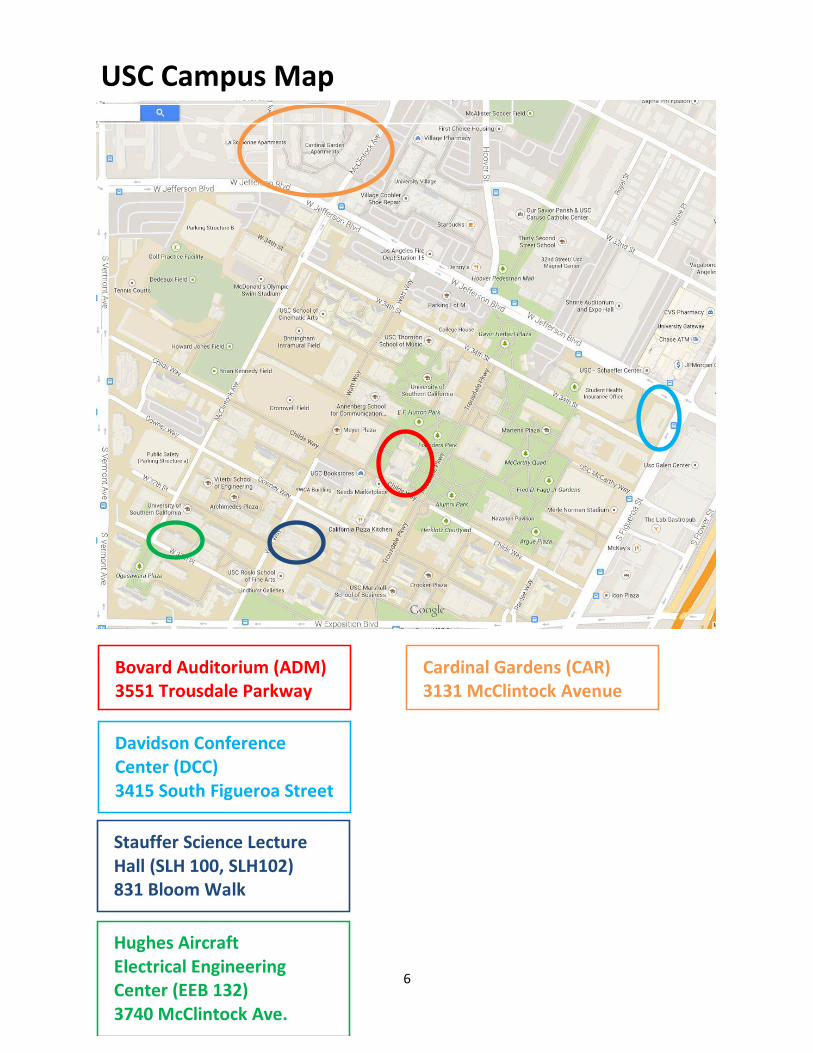
6
Bovard Auditorium (ADM) 3551 Trousdale Parkway
Davidson Conference Center (DCC) 3415 South Figueroa Street
Stauffer Science Lecture Hall (SLH 100, SLH102) 831 Bloom Walk
Hughes Aircraft Electrical Engineering Center (EEB 132) 3740 McClintock Ave.
Cardinal Gardens (CAR) 3131 McClintock Avenue
USC Campus Map USC Campus Map
7
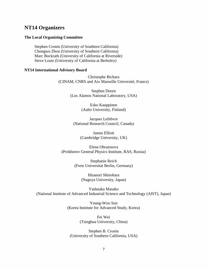
NT14 Organizers
The Local Organizing Committee
Stephen Cronin (University of Southern California)
Chongwu Zhou (University of Southern California)
Marc Bockrath (University of California at Riverside)
Steve Louie (University of California at Berkeley)
NT14 International Advisory Board
Christophe Bichara
(CINAM, CNRS and Aix Marseille Université, France)
Stephen Doorn
(Los Alamos National Laboratory, USA)
Esko Kauppinen
(Aalto University, Finland)
Jacques Lefebvre
(National Research Council, Canada)
James Elliott
(Cambridge University, UK)
Elena Obraztsova
(Prokhorov General Physics Institute, RAS, Russia)
Stephanie Reich
(Freie Universitat Berlin, Germany)
Hisanori Shinohara
(Nagoya University, Japan)
Yudasaka Masako
(National Institute of Advanced Industrial Science and Technology (AIST), Japan)
Young-Woo Son
(Korea Institute for Advanced Study, Korea)
Fei Wei
(Tsinghua University, China)
Stephen B. Cronin
(University of Southern California, USA)
8
Partners and Sponsors
Finacial Support US Department of Energy
National Science Foundation
Ming Hsieh Insititute, USC
USC Viterbi School of Engineering
Exhibitors Aixtron (Silver Sponsor)
WITec
Bruker
Renishaw
NanoIntegris
Amercian Elements
9
Charter of the Nanotube (NT) Conference Series
http://nanotube.msu.edu/nt/charter.html
1. Purpose.
The purpose of the NT conference series is to promote scientific progress, to stimulate free
exchange of ideas, and to publicize progress in nanotube sciences.
2. Target attendance.
2.1 NT conferences are open to all persons interested and active in nanotube research.
2.2 The number of attendees or presentations per attendee may be limited to maintain the
informal spirit of communication. Young researchers are treated with higher priority.
3. Format.
3.1 The organizers will assist in maximizing opportunities for sharing knowledge in an informal
atmosphere.
3.2 NT conferences are held in one single plenary session. Parallel sessions are to be avoided.
3.3 Presentations of problems and needs is encouraged as much as presentation of solutions.
3.4 Contributions play a key role at NT conferences. At least half the conference time shall be
devoted to contributed presentations.
4. Contributed presentations.
4.1 To provide maximum exposure to contributed results, contributors are invited to summarize
their findings in a Poster format. The main purpose of Poster presentations is to facilitate
asynchronous scientific discussions related to each specific contribution. It is desirable to have
all posters on display during the entire conference.
4.2 The organizers secure adequate time and space for poster sessions. Creative ways to enhance
communications, including refreshments, are encouraged.
4.3 Poster+ sessions, consisting of brief 2 minute/2 viewgraph summaries of contributions, may
precede Poster sessions, to enhance the exchange of information in a balanced manner. All
contributors are encouraged to expose their findings to everyone in this way if Poster+ sessions
are offered.
4.4 At large conferences, Poster+ presentations may be substituted by a brief overview of the
topic of a focussed poster session, presented by an expert in the field at the beginning of the
session. Referring to specific contributions in the session, the Poster Chair should summarize the
major progress, the major obstacles, and desirable future directions in the field. Ideally, this
should occur in a democratic manner, representing all/most contributions. All contributors are
encouraged to communicate their findings to their assigned Poster Chair for presentation well
ahead of the conference.
5. Invited presentations.
5.1 Invited presentations are selected in a democratic way by members of the advisory board.
Presentation of invited talks is reserved for leading, active researchers, not their substitutes. The
selection of topics and speakers should reflect the most significant progress and cover the entire
active nanotube field. The advisors will resist pressure to select invited talks on other grounds
than scientific merit.
10
5.2 NT conference organizers should generally avoid inviting the same presenter at two
consecutive conferences. To avoid conflicts of interest, the organizers should generally avoid
inviting contributions of organizers and advisory board members.
6. Venue.
6.1 To pay respect to the international character of nanotube research, two consecutive meetings
should not be held on the same continent.
6.2 The conference should preferentially be held a location associated with or close to an
institution active in nanotube research.
6.3 Convenience of the conference facilities is preferred to luxury. Modest conference
accommodations are to be preferred to reduce the conference expenses of participants and to
encourage attendance.
7. Financial matters.
7.1 NT conferences are organized in a non-profit way. The organizers undertake any reasonable
efforts to secure external sponsorship covering local and travel expenses of invited speakers,
support student attendance, and reduce the conference fee. Any excess revenue is passed on to
organizers of the sequel conference.
7.2 Financial liability for the NT conference rests with the organizers.
8. Satellite symposia.
8.1 Satellite symposia form an integral part of NT conferences.
8.2 Logistics of satellite symposia is taken care of by the NT conference, the scientific program
is left to the satellite organizers.
8.3. At least one of the satellite symposium organizers is member of the national committee of
the NT conference.
9. Miscellaneous.
9.1 NT organizers promote the spirit of informal communication also by providing name badges
to participants. Both first and family names should be spelled out and printed in an easily legible,
large font. Academic titles should be avoided.
10. Regulation.
All issues related to the organization of Nanotube Conferences are regulated by theSteering
Committee of Nanotube Conferences (SCNC).

11
12
K1
Carbon Nanotubes: From Basic Research to Commercialization
Shoushan Fan
Department of Physics & Tsinghua‐Foxconn Nanotechnology Research Center, Tsinghua
University, Beijing, Beijing, China
Carbon nanotube (CNT) is a promising nanomaterial for real applications due to its excellent
mechanical, electrical, and thermal properties. The real products of CNT are expected after long
time intensive research efforts on it. In this talk, I will present our research works on CNTs in the
past two decades, including studies on the growth mechanism, controllable synthesis, physical
properties, and real applications of CNTs. In particular, I will show that a unique macroscopic
form of CNTs, the super-aligned CNTs, can bridge the gap between nano-world and macro-
world and lead CNTs into real applications.[1-7] Many real applications, such as field and
thermionic emission electron sources,[8-12] high strength CNT yarns,[2,6,7] electrodes for batteries
and supercapacitors,[13-17] loudspeakers,[18,19] displays,[20-22] SERS substrate,[23] IR detector[24] etc.
have been demonstrated. Real products of CNT TEM grids [25,26] and CNT touch panels[4] have
already been commercialized. More products based on super-aligned CNTs are expected to go to
the market in the near future.[27]
[1]. K. L. Jiang, Q. Q. Li, S. S. Fan, Nature 2002, 419, 801
[2]. X. B. Zhang, K. L. Jiang, et al. Adv. Mater. 2006, 18, 1505
[3]. K. Liu, et al. Nano Lett. 2008, 8, 700
[4]. C. Feng, K. Liu, et al. Adv. Funct. Mater.2010, 20, 885
[5]. K. Liu, Y. H. Sun et al. Adv. Funct. Mater.2011, 21, 2721
[6]. K. Liu, Y. H. Sun, et al. Nanotechnology 2010, 21, 045708
[7]. K. Liu, Y. H. Sun, et al. ACS Nano 2010, 4,5827
[8]. Y. Wei, et al. Appl. Phys. Lett. 2006, 89, 063101
[9]. P. Liu, Y. Wei, K. L. Jiang et al. Phys. Rev. B. 2006, 73, 235412
[10]. Y. Wei, K. L. Jiang, X. F. Feng, P. Liu, L. Liang, S. S. Fan, Phys. Rev. B. 2007, 76, 045423
[11]. Y. Wei, K. L. Jiang, L. Liang, Z. Chen, S. S. Fan, Nano Lett. 2007, 7, 3792
[12]. L. Xiao, et al. Appl. Phys. Lett. 2008, 92, 153108
[13]. H. X. Zhang, C. Feng, et al. Adv. Mater. 2009, 21, 2299
[14]. R. F. Zhou, et al. Nanotechnology 2010, 21, 345701
[15]. S. Luo, et al. Adv. Mater. 2012, 24, 2294
[16]. Y. Wu, et al. Nano Lett. 2013, 13, 818
[17]. K. Wang, et al. Adv. Func. Mater.2013, 23, 846
[18]. L. Xiao et al., Nano Lett. 2008, 8, 4539
[19]. L. Xiao et al., J. Appl. Phys. 2011, 110, 084311
[20]. P. Liu, et al. Adv. Mater. 2009, 21, 3563.
[21]. P. Liu, et al. Nano Lett. 2012, 12, 2391
[22]. Y. Wei, et al. Nano Lett. 2012, 12, 2548
13
[23]. Y. H. Sun, et al. Nano Lett. 2010, 10, 1747.
[24]. L. Xiao et al., Nanotechnology, 2011, 22, 025502.
[25]. L. N. Zhang, et al. Nano Lett. 2008, 8, 2564.
[26]. L. N. Zhang, et al. Nanotechnology, 2011, 22,385704
[27]. K. L. Jiang, et al. Adv Mater. 2011, 23, 1154.
I1
Atomic Carbon Chains: A Perfectly One-Dimensional Carbon Phase
Beyond Nanotubes
F. Banhart, O. Cretu, A. La Torre, A. Botello-Mendez, J. -C Charlier
Institut de Physique et Chimie des Matériaux, University of Strasbourg, Strasbourg, Alsace,
France
Institute of Condensed Matter and Nanosciences, Université catholique de Louvain, Louvain,
Walloon Brabant, Belgium
Carbon chains can be considered as sp1-hybridized strings of carbon atoms of monoatomic
thickness, constituting the logical one-dimensional phase of carbon. They have been proposed
since a long time until they were observed by electron microscopy. Recent experiments show
that, by using a measuring system with an STM tip in a TEM specimen stage, carbon chains can
not only be made but also characterized (O. Cretu et al., Nano Lett. 13, 3487 (2013)). By passing
a current through the chains, their electrical properties have been measured for the first time. The
chains are obtained by unraveling carbon atoms from nanotubes or graphene ribbons while an
electrical current flowed through the tubes or ribbons and, successively, through the chain. The
electrical conductivity of the chains was found to be much lower than predicted for ideal chains.
First-principles calculations show that strain in the chains determines the conductivity in a
decisive way. Indeed, carbon chains are always under varying non-zero strain that transforms
their atomic structure from cumulene (double bonds throughout the chain) to polyyne
(alternating single/triple bonds), thus inducing a tunable band gap. New experiments show the
bonding characteristics at contacts between metals and carbon chains as well as characteristic
current-voltage curves, depending on the type of contact. The experiments show a perspective
toward the synthesis of carbon chains and their application as the smallest possible interconnects
or even as one-dimensional semiconducting devices.
14
CT1
Coherent phonon spectra of G band in single wall carbon nanotubes
Ahmad R. T. Nugraha, Eddwi H. Hasdeo, Riichiro Saito
Department of Physics, Tohoku University, Sendai, Miyagi, Japan
In ultrafast (femtosecond) pump-probe spectroscopy, coherent phonons have been known to be
observed in terms of oscillations of the change in optical constants (e.g. reflectivity and
transmittance) as a function of delay time between pump and probe pulses, in which these
oscillations are directly related to the modulations of absorption coefficient. For a single wall
carbon nanotube (SWNT), Fourier power spectra of the differential reflectivity or transmittance
as a function of phonon frequency show several peaks that correspond to the SWNT’s coherent
phonon modes, such as the radial breathing mode (RBM), G band, and even acoustic modes. [1,2]
In the case of RBM, oscillations of optical constants are already understood as a result of a
diameter-dependent band gap.[3,4] However, this mechanism cannot be used for the other phonon
modes. In particular, if we consider the same mechanism for the G-band, it was previously
predicted that the modulations of absorption coefficient due to G-band phonons are about 1000
times smaller than those caused by the RBM.[5] However, recent experiments showed that the
coherent G-band signal is comparable to, and almost on the same order as, the RBM signal. [6]
In this work, we present an origin of the strong coherent G-band signal. Instead of the energy gap
modulations as in the RBM, here we expect that the modulations of electron-photon interaction
as a function of time should be relevant to the coherent G-band intensity. We also compare the
coherent G-band intensity with the other coherent phonon modes in a specified SWNT chirality.
We expect that there might be a common origin of the coherent phonon spectral line shapes of
any materials due to changes of phase in the coherent oscillations. This theory could be a
significant progress for understanding a general and systematic behavior of coherent phonons.
[1]. A. Gambetta et al., Nat. Phys. 2, 515-520 (2006)
[2]. Y.-S. Lim, A. R. T. Nugraha, et al., Nano Lett. (2014), in press. DOI: 10.1021/nl404536b
[3]. A. R. T. Nugraha et al., Phys. Rev. B 84, 174302 (2011)
[4]. A. R. T. Nugraha et al., Phys. Rev. B 88, 075440 (2013)
[5]. G. D. Sanders et al., Phys. Rev. B 79, 205434 (2009)
[6]. J.-H. Kim et al, Phys. Rev. B 86, 161415 (2012)
15
CT2
Single-Walled Carbon Nanotube Networks for Ethanol Vapor
Sensing Application
Albert Nasibulin, Ilya Anoshkin, Prasantha Mudimela, Maoshuai He, Vladimir Ermolov, Oleg
Tolochko, Esko Kauppinen
Dept. Applied Physics, Aalto University, Espoo, Uusimaa, Finland
Nokia Research Center, Nokia, Espoo, Uusimaa, Finland
Institute of Materials and Technologies, Saint-Petersburg Polytechnic State University, Saint-
Petersburg, Russia, Russian Federation
Dept. Applied Physics, Aalto University, Espoo, Uusimaa, Finland
Networks of pristine high quality single walled carbon nanotubes (SWNTs), the SWNTs after
Ar-plasma treatment (from 2 to 12 min) and carbon nanobuds (CNBs) have been tested for
ethanol vapor sensing. It was found that the pristine high quality SWNTs do not exhibit any
ethanol sensitivity, while the defect introduction in the tubes results in the appearance of the
ethanol sensitivity. The CNB network showed the ethanol sensitivity without plasma treatment.
Both CNB and low defective (after 3 min treatment) SWNT networks exhibit significant drift in
the resistance baseline, while heavily plasma-treated (9 min) SWNTs exhibited high ethanol
vapor sensitivity without the baseline change. The mechanisms of the ethanol sensitivity and
stability after the plasma irradiation are attributed to the formation of sensitive dangling bonds in
the SWNTs and formation of defect channels facilitating an access of the ethanol vapor to all
parts of the bundled nanotubes.

16
Posters 1+2 Summary (David Tomanek)

17
Poster Session 1 and Exhibition
18
I2
Giant Currents and Temperatures for Coulomb Blockade during
Field Emission from Single Wall Carbon Nanotubes
S. Perisanu, A. Pascale-Hamri, A. Derouet, C. Journet,P. Vincent, A. Ayari, S. T. Purcell
Institut Lumière Matière, Université Claude Bernard Lyon 1 and CNRS, Villeurbanne, Lyon,
The Coulomb Blockade (CB) has been and continues to be studied intensively for its interest in
fundamental physics and technology. Two important limitations of CB devices are low operating
currents, now reported up to ~100 nA, and poor room temperature performance. The later has
been improved over the years by fabricating ever smaller structures, in particular when the
Coulomb island is a Single Wall Carbon Nanotube (SWCNT). We present here well-defined
Coulomb staircases (CS), using an original Field Emission (FE) experiment on several individual
in-situ grown SWCNT cantilevers. Additional individual electrons on the SWCNTs were
detected in FE currents and mechanical resonance eigenfrequencies. Results quantitatively agree
with CB FE theory developed by Raichev. A unique in-situ shortening technique was applied
nine times to one SWCNT to increase progressively the oscillations periods from 5.5 V to 80V,
the temperature for observable CS to 1100 K and the currents to 1.8 µA, all the largest values
found in the literature (to the best of our knowledge). This process led to the brightest electron
source reported (9x10¹¹A/(str.m2.V)).
19
CT3
Automated Carbon Nanotube Synthesis by Water-assisted CVD
Pavel Nikolaev, Daylond Hooper, Benji Maruyama
UES Inc., Dayton, OH, United States
Materials and Manufacturing Directorate, RXAS, Air Force Research Laboratory, WPAFB, OH,
United States
Among many techniques of carbon nanotube (CNT) synthesis available today, chemical vapor
deposition (CVD) is the most popular by far due to low cost, ease of set-up, and wide range of
nanotube morphologies that can be produced. The throughput of a typical research CVD system,
however, is limited to a few runs per day due to time necessary for heating, conditioning,
growing, and cooling steps. This makes it difficult and time-consuming to explore the multi-
dimensional experimental parameter space that includes temperature, pressure, feedstock
composition; catalyst and catalyst support composition. The Adaptive Rapid Experimentation
and in-situ Spectroscopy (ARES) CVD system described in this contribution makes over 100
CVD experiments possible in a single day in fully automatic mode, with pre-programmed growth
recipes and without user intervention. CNTs are grown in a miniature cold wall CVD reactor,
with the same laser used for both thermal activation of the growth process and Raman excitation.
Raman spectra are acquired in real time, enabling in-situ analysis of growth kinetics and
nanotube characteristics. Further linear regression modeling allowed mapping regions of
selectivity towards SWNT and MWNT growth in the complex parameter space of the water-
assisted CVD synthesis. This is the first demonstration of automated experimentation combined
with regression analysis applied to the CNT synthesis by CVD. This development of the
automated rapid serial experimentation is a significant progress towards an autonomous closed-
loop learning system: a Robot Scientist.
20
CT4
Giant Nonlinear Optical Response from Dye-filled Carbon
Nanotube Hybrids
Jochen Campo, Sofie Cambré, Charlie Beirnaert, Christof C. Verlackt, Wim Wenseleers
Physics Department, University of Antwerp, Wilrijk, Antwerp, Belgium
Asymmetric dipolar molecules, acting as electric ‘rectifiers’ with a large second-order nonlinear
optical (NLO) response (first hyperpolarisability β), find applications in ultrafast electro-optic
switches for optical telecommunication networks and wavelength conversion of lasers.[1] In 3D
bulk systems, however, such dipolar molecules tend to align in a pairwise anti-parallel way, thus
cancelling each other’s directional properties, such as the NLO response. Parallel alignment is
traditionally achieved by electric field poling in a polymer matrix, but long term stability of this
alignment remains problematic.
Here we show that by encapsulating such elongated dipolar molecules in the 1D internal channel
of single-wall carbon nanotubes (SWCNTs), Coulomb interactions naturally favor a polar head-
to-tail alignment of the molecular dipoles, leading to a cooperative enhancement of their second-
order NLO responses. This principle is demonstrated for a prototypical dipolar molecule
encapsulated in various SWCNT samples. The encapsulation is evidenced by extensive
wavelength-dependent fluorescence-excitation[2] and resonance Raman[3] experiments on bile-
salt solubilized[4] dye-filled SWCNTs, revealing the effect of encapsulation on the vibrational
and electronic properties of the SWCNTs and the encapsulated molecules. Wavelength-
dependent hyper-Rayleigh scattering[5,6] (i.e. second harmonic light scattering) experiments
effectively show that these organic-SWCNT nanohybrids possess giant NLO responses (β =
68800 x 10-30 esu at resonance; β0 = 9770 x 10-30 esu in the static limit; corresponding to ~70
identically aligned chromophores, depending on the SWCNT diameter range). Their equally
giant dipole moment and size promises a good and stable alignment of the nanohybrids in a
polymer film, which opens up an entirely new route to the rational design of solution-processible
yet stable NLO materials.
[1]. E. Goovaerts et al. In Handbook of advanced electronic and photonic Materials and Devices,
Vol. 9: Nonlinear optical materials, Academic Press, San Diego, 127-191 (2001)
[2]. S. Cambré et al., ACS nano 6, 2649 (2012)
[3]. W. Wenseleers et al., Adv. Mater. 19, 2274 (2007)
[4]. W. Wenseleers et al., Adv. Funct. Mater. 14, 1105 (2004)
[5]. J. Campo et al., Optics Express 17, 4587 (2009)
[6]. J. Campo et al., J. Phys. Chem. Lett. 3, 2248 (2012)
21
CT5
Radial Deformation of Single-Walled Carbon Nanotubes on Quartz
Substrates and the Resultant Anomalous Diameter-Dependent
Reaction Selectivity
Juan Yang, Yu Liu, Daqi Zhang, Xiao Wang, Yan Li
College of Chemistry and Molecular Engineering, Peking University, Beijing, Beijing, China
Owing to the unique conjugated structure, chemical reaction selectivity of single-walled carbon
nanotubes (SWNTs) has attracted great attentions. By utilizing the radial deformation of SWNTs
caused by the strong interactions with the quartz lattice, we achieve an anomalous diameter-
dependent reaction selectivity of quartz lattice-oriented SWNTs in treatment with iodine vapor,
which is distinctly different from the widely reported and well accepted higher reaction activity
in small-diameter tubes over the large ones. The radial deformation of SWNTs on quartz
substrate is verified by detailed Raman spectra and mappings in both G band and RBM. Due to
the strong interaction between SWNTs and the quartz lattice, large-diameter tubes present larger
degree of radial deformation and more delocalized partial electrons are distributed at certain
sidewall sites with high local curvature. It is thus easier for the carbon-carbon bonds at those
high curvature sites on large-diameter tubes to break down upon reaction. This anomalous
reaction activity offers a novel approach for selective removal of small-bandgap large-diameter
tubes.

22
Poster Sesssion 2 + Exhibition
23
CT6
Ultrafast charge photogeneration and dynamics in semiconducting
carbon nanotubes
Giancarlo Soavi, Francesco Scotognella, Daniele Viola, Timo Hefner, Tobias Hertel, Giulio
Cerullo, Guglielmo Lanzani
Dipartimento di Fisica, Politecnico di Milano, Milano, Lombardia, Italy
Dept. of Chemistry and Pharmacy, Inst. for Physical and Theoretical Chemistry, University of
Würzburg , Würzburg, Bavaria, Germany
Dipartimento di Fisica, Politecnico di Milano, Milano, Lombardia, Italy
Center for Nano Science and Technology@PoliMi, Istituto Italiano di Tecnologia, Milano,
Lombardia, Italy
Single-walled carbon nanotubes (SWNTs) are excellent model systems for the study of
photoexcitation dynamics in one-dimensional (1D) quantum confined systems. Theory predicts
that Wannier-Mott excitons are the elementary photoexcitations in SWNTs, due to the strong
Coulomb interaction caused by the weak screening. Such excitons have peculiar 1D
characteristics, such as extraordinary large binding energies, large size and 1D transport.
Experimental observations, such as the measured binding energy, typically 0.1-1 eV, and the
electron-hole correlation length, in the 1-10 nm domain confirm theoretical predictions. The
exciton model alone, however, fails to capture the whole dynamics following photoexcitation,
and many other photoexcited species have crowded the complex scenario of SWNTs’ optical
response, ranging from triplets to bi-excitons and trions. Experiments based on photocurrent,
transient absorption and THz spectroscopy also point out a non-negligible photogeneration of
free charge-carriers. This is in contrast with the excitonic model and the reduced Sommerfeld
factor that predicts that excitons should be the only species generated upon photoexcitation.
Attempts to solve this discrepancy proposed non-linear processes, such as exciton-exciton
annihilation, as a mechanism of charge-carrier photogeneration. However, there is solid
experimental evidence that charge-carrier photogeneration is linear with the pump fluence.
Here we apply broadband ultrafast transient absorption spectroscopy to the semiconducting (6,5)
SWNT and show that charge-carriers can be identified by their effect on excitonic resonances, in
particular the large Stark shift that they induce on high-energy, easily polarizable excitons (S22
and S33). Having identified the Stark shift as a good spectroscopic fingerprint for charge-carriers,
we are able to study their dynamics in a nearly ideal 1D system. We find that a fraction of the
absorbed photons generates geminate charge-carrier pairs within our temporal resolution (≈ 50
fs), which then recombine on the picosecond timescale following the characteristic kinetic law of
random walk in 1D. Our analysis starts from the observation that the first derivative of the
ground state absorption spectrum, i.e. a photoinduced red shift of the excitonic transition, can
reproduce many of the features observed in the differential transmission (ΔT/T) spectra of
semiconducting SWNTs. This effect can be ascribed to different physical mechanisms, such as

24
bi-excitons or trions formation, thermal effects or Stark effect. Here we unambiguously
demonstrate that this derivative shape is indeed due to strong local electric field induced by
photogenerated charge-carriers, which shifts the electronic transitions by Stark effect. In
particular, we show that the energy shift is stronger for excitons with lower binding energy, as
for S33 with respect to S11, as expected for the Stark effect. This suggests that the higher energy
S33 exciton is ideally suited for directly probing charge-carriers in SWNTs and can be exploited
to further analyze the charge photogeneration process and to study charge-carrier dynamics in
one dimension. Our data show that the free charge- carriers are generated within 50 fs. The
temporal evolution of the S33 pump-probe dynamics is very accurately reproduced by a power
law ̴ t-0.5. A monomolecular power law decay is the predicted dynamics for geminate
recombination of free particles after random walk in an infinite one-dimensional chain. A more
detailed modelling of the geminate recombination process indicates that the initial distance
between the geminate e-h pair is of the same order of magnitude of the exciton correlation length,
thus suggesting that charge-carriers arise from instantaneous linear exciton dissociation.
Our results shed new light onto the charge photogeneration mechanism in SWNTs, suggesting
that the nascent exciton dissociates spontaneously, perhaps in presence of extrinsic screening of
the Coulomb attraction, possibly due to water or other ambient contamination.
25
I3
Electronic properties in moiré superlattice in rotationally stacked
atomic layers
Mikito Koshino, Pilkyung Moon
Department of Physics, Tohoku University, Sendai, Miyagi, Japan
School of Computational Sciences, Korean Institute for Advanced Study, Dongdaemun-gu, Seoul,
Korea, Republic Of
We report recent theoretical studies on the electronic properties of rotationally stacked atomic
layer systems, including graphene-graphene bilayer, and graphene-hBN (hexagonal boron nitride)
composite bilayer. The misoriented atomic structure gives rise to a moiré superlattice structure
with a long spatial period, and it strongly modifies the band structure in the low-energy region.
We develop an effective continuum model based the tight-binding Hamiltonian, which correctly
describes the electronic structure of moiré superlattice.[1] In a magnetic field, the coexistence of
the moiré pattern and the Landau quantization causes the fractal energy spectrum so-called
Hofstadter’s butterfly. We calculate the spectral evolution as a function of magnetic field, and
demonstrate that the quantized Hall conductivity changes in a complicated manner in changing
Fermi energy and the magnetic field amplitude.[2] We also calculate the optical absorption in the
fractal band regime, and find that the absorption spectrum and the optical selection rule exhibit
recursive self-similar structure as well, reflecting the fractal nature of the energy spectrum.[3]
[1]. P. Moon and M. Koshino, Phys. Rev. B 87, 205404 (2013)
[2]. P. Moon and M. Koshino, Phys. Rev. B 85, 195458 (2012)
[3]. P. Moon and M. Koshino, Phys. Rev. B 88, 241412(R) (2013)
26
Poster Session 1
T1
Coherent phonon spectra of G band in single wall carbon nanotubes
Ahmad R. T. Nugraha, Eddwi H. Hasdeo, Riichiro Saito
Department of Physics, Tohoku University, Sendai, Miyagi
In ultrafast (femtosecond) pump-probe spectroscopy, coherent phonons have been known to be
observed in terms of oscillations of the change in optical constants (e.g. reflectivity and
transmittance) as a function of delay time between pump and probe pulses, in which these
oscillations are directly related to the modulations of absorption coefficient. For a single wall
carbon nanotube (SWNT), Fourier power spectra of the differential reflectivity or transmittance
as a function of phonon frequency show several peaks that correspond to the SWNT’s coherent
phonon modes, such as the radial breathing mode (RBM), G band, and even acoustic modes.[1,2]
In the case of RBM, oscillations of optical constants are already understood as a result of a
diameter-dependent band gap.[3,4] However, this mechanism cannot be used for the other phonon
modes. In particular, if we consider the same mechanism for the G-band, it was previously
predicted that the modulations of absorption coefficient due to G-band phonons are about 1000
times smaller than those caused by the RBM.[5] However, recent experiments showed that the
coherent G-band signal is comparable to, and almost on the same order as, the RBM signal.[6]
In this work, we present an origin of the strong coherent G-band signal. Instead of the energy gap
modulations as in the RBM, here we expect that the modulations of electron-photon interaction
as a function of time should be relevant to the coherent G-band intensity. We also compare the
coherent G-band intensity with the other coherent phonon modes in a specified SWNT chirality.
We expect that there might be a common origin of the coherent phonon spectral line shapes of
any materials due to changes of phase in the coherent oscillations. This theory could be a
significant progress for understanding a general and systematic behavior of coherent phonons.
[1]. A. Gambetta et al., Nat. Phys. 2, 515-520 (2006)
[2]. Y.-S. Lim, A. R. T. Nugraha, et al., Nano Lett. (2014), in press. DOI: 10.1021/nl404536b
[3]. A. R. T. Nugraha et al., Phys. Rev. B 84, 174302 (2011)
[4]. A. R. T. Nugraha et al., Phys. Rev. B 88, 075440 (2013)
[5]. G. D. Sanders et al., Phys. Rev. B 79, 205434 (2009)
[6]. J.-H. Kim et al, Phys. Rev. B 86, 161415 (2012)

27
T2
Quantum interference effect in Raman spectra of metallic
nanotubes
Eddwi H. Hasdeo, Ahmad R. T. Nugraha, Mildred S. Dresselhaus, Riichiro Saito
Department of Physics, Tohoku University, Sendai, Miyagi, Japan
Department of Physics, MIT, Cambridge, MA, United States
Department of Physics, Tohoku University, Sendai, Miyagi, Japan
In graphene and metallic single wall carbon nanotubes (m-SWNTs), the existence of gapless
linear energy bands (Dirac cones) modify the G band (in-plane optical phonon modes) Raman
spectra. One of the well-known phenomena is the Kohn anomaly effect, in which the phonon
energy (lifetime) becomes lower (shorter) due to the interaction between the G phonon and an
electron-hole pair in the linear energy band.[1] The other phenomenon is the asymmetric spectral
shape of the G band, also known as Breit-Wigner-Fano (BWF) line shape, which long been
observed in m-SWNTs[2] and recently observed in graphene.[3] However, the origin of this BWF
lineshape asymmetry remains a question. In this presentation, the origin of BWF line shape is
explained by means of quantum interference of phonon G band spectra and electronic Raman
spectra (ERS).[4] The ERS are electronic spectra whose origin comes from an electron-hole pair
excitation in the vicinity of the Dirac cone.[5]
In this work, we calculated the exciton-exciton interaction between a photo-excited exciton and
an exciton in the linear band of a m-SWNT which is relevant to the ERS. We calculated ERS
spectra as a function of laser excitation energy and we reproduced the experimental BWF
spectral shape for all laser excitation energies. The Coulomb potential, generally, gives a
maximum value at momentum transfer q=0 but surprisingly, we found that the direct Coulomb
interaction between the two excitons vanishes at q=0. The absence of the direct Coulomb
interaction is due to the symmetry of the two sub-lattices of SWNTs unit cell. Using the same
method, we extend the story in graphene and reproduce the experimental result of the G band
asymmetry as a function of Fermi energy. We also predict that the radial breathing phonon mode
(RBM) spectra in m-SWNTs exhibit the opposite BWF asymmetry to that of the G band, by
showing the laser energy dependence of RBM spectra.
[1]. “Raman spectroscopy in graphene related systems”, A. Jorio et al, Wiley (2011)
[2]. S. D. M. Brown et al., Phys. Rev. B 63, 155414, (2001)
[3]. D. Yoon et al., Carbon, 61, 373-378, (2013)
[4]. E. H. Hasdeo et al.Phys. Rev. B 88, 115107, (2013)
[5]. H. Farhat et al., Phys. Rev. Lett. 107, 157401 (2011)
28
T3
Spontaneous formation of O8 clusters and chains within
nanostructures
Daniel Vasconcelos Pazzini Massote, Mário Sérgio Mazzoni
Physics Department, Universidade Federal de Minas Gerais, Belo Horizonte, Minas Gerais,
Brazil
We perform first principles calculations based on the density functional theory to show that the
building blocks of the oxygen ε-high pressure solid phase spontaneously form when oxygen
molecules are enclosed within fullerenes and small diameter nanotubes. We observe that the
stability increases with the enclosure diameter. The building blocks consist in O8 clusters, which
are able to self-assemble into periodic arrays inside nanotubes. Such chains are semiconductors
when isolated or when encapsulated in boron nitride nanotubes, and become doped when
confined in carbon materials. In the same way as we observe a magnetic collapse in oxygen ε
solid phase, these O8 clusters maintain this property when encapsulated. Molecular dynamics
simulations confirm the formation and stability of the clusters and chains in ambient conditions.
29
T4
Wave propagation along coplanar transmission line covered with
inkjet printed multi-walled carbon nanotubes network
Ibtissem Oueriemi1, Jean-Pierre Raskin, Fethi Choubani, Vedi Dupont, Véronique Lardot,
Isabelle Huynen
ICTEAM-ELEN, Université catholique de Louvain, Louvain-la-Neuve, Brabant-wallon, Belgium
Innov’Com Lab, Higher school of Communications of Tunis, El Ghazala, Ariana, Tunisia
Belgium Ceramics Research Center, université de Mons, Mons, Brabant-wallon, Belgium
ICTEAM-ELEN, Université catholique de Louvain, Louvain-la-Neuve, Brabant-wallon, Belgium
The trend of device minimization in size, weight and cost for use in commercial wireless
communication systems has resulted in an increasing demand for highly integrated system-on-
chip solutions. To shrink the size of interconnections and passive devices, many researchers have
proposed the use of slow-wave propagation mode in order to reduce the effective electrical
wavelength of the RF signals.[1]
On the other hand, carbon nanotubes (CNTs) are emerging as novel nanomaterial for a large
variety of applications, particularly as electronic material owing to their amazing mechanical,
thermal and unique electrical properties.[2] Thin films of CNTs networks/arrays, a planar
topology is usually preferred, with in view the application to CNT-based interconnects and
carbon-based circuits.[3] The use of CNTs network could bring solutions to reduce the size of
microwaves circuits in addition to the benefit of short-time and low-cost fabrication using inkjet
printing. Furthermore, this technique gives the possibility to readily control the pattern geometry,
location, film thickness, and uniformity of the films.
In this present study, we aim at investigating the mode propagation when multi-walled carbon
nanotubes (MWCNTs) ink is used to print films on coplanar waveguides (CPWs) lying on glass
substrate. The extracted line characteristics from measured S-parameters offer an accurate
analysis of the propagation mechanism, revealing the existence of a slow-wave mode regime. A
good master of this property is appropriate for exploiting the slow-wave phenomenon in order to
scale down the size of passive integrated structures. Thus, the impact of geometry and the
number of alternate deposited CNTs networks are experimentally tested.
[1]. R. Saito, M. Fujita, G. Dresselhaus, and M. S. Dresselhaus, Appl. Phys. Lett., 60, p. 2204,
1992
[2]. J. Sor, Y. Qian, and T. Itoh, IEEE Trans. Microwave Theory Techn., vol. 49, pp. 2336-2341,
Dec. 2001
[3]. M. A. El Sabbagh, Proceedings of IEEE International Symposium on Electromagnetic
Compatibility (EMC), pp. 841-846, July 2010
30
T5
Phase diagram of Ni-C nanoparticles from computer simulation
Yann Magnin
CINaM TSN, CNRS, Marseille, Bouche du Rhône, France
Carbon nanotube synthesis critically depends on the chemical and physical states of the catalyst
particle from which they grow. In the typical temperature range (600-1000 °C) of SWNT
synthesis, pure isolated Ni nanoparticles are solid although atomic diffusion can lead to
significant shape changes. Under growth conditions, these nanoparticles are exposed to reactive
carbon. Depending on temperature, carbon chemical potential and nanoparticle size, carbon can
either stay adsorbed on the surface, or diffuse to subsurface or in the core of the nanoparticle,
thereby inducing a partial or complete melting.
On the basis of the tight binding model developed for the Ni-C system coupled with grand
canonical Monte Carlo simulations,[1]we try and calculate size dependent liquid/solid phase
diagrams for Ni-C alloys. We thus extend our previous calculations[2,3] and rationalize our
findings using suitable order parameters, as proposed by Steinhardt et al. [4]
[1]. H. Amara et al., Phys. Rev. B 79, 014109 (2009)
[2]. M. Diarra et al., Phys. Stat. Sol. B 249, 12, 2629–2634 (2012)
[3]. M. Diarra et al., Phys. Rev. Lett. 109, 185501 (2012)
[4]. P. Steinhardt, D. Nelson, and M. Ronchetti, “Bond-orientational order in liquids and glasses,”
Phys. Rev. B, 28, 2, 784–805 (1983)
31
T6
Is exciton BEC possible in individual carbon nanotubes?
A theoretical prospective
Igor Bondarev
Math and Physics, North Carolina Central University, Durham, NC, United States
I will tell about one interesting possibility that we have lately theoretically demonstrated to exist
for the 1D exciton Bose-Einstein condensation (BEC) phenomenon in individual small-diameter
(∼1−2 nm) semiconducting carbon nanotubes (CNs).[1] This originates from the strong coupling
of excitons and low-energy inter-band plasmons enabled via the quantum confined Stark effect
by using an external electrostatic field applied perpendicular to the CN axis. The perpendicular
electrostatic field mixes excitons and inter-band plasmons of the same band,[2] to result in
strongly coupled hybridized excitations-exciton-plasmons in one individual CN.[3] Such
hybridized excitations are strongly correlated collective Bose-type quasi-particles and, therefore,
could likely be condensed under appropriately created external conditions ― in spite of the well-
known statements of the BEC impossibility in ideal 1D/2D systems[4] and experimental evidence
reported earlier for no exciton BEC effect in CNs.[5] Possibilities for achieving BEC in 1D/2D
systems are theoretically demonstrated earlier in the presence of an extra confinement potential.[6]
The correlated exciton-plasmon system in a CN presents such a special case. The effect requires
fields∼1 V/nm and temperatures below 100 K that are experimentally accessible.[7]The effect
offers a testing ground for fundamentals of 1D condensed matter physics and opens up
perspectives to develop a tunable highly coherent polarized light source with CNs.
This research is supported by the US Department of Energy (DE-SC0007117).
[1]. I.V. Bondarev and A.V. Meliksetyan, Phys. Rev. B 89, 045414 (2014)
[2]. I.V. Bondarev, L.M. Woods, and K. Tatur, Phys. Rev. B 80, 085407 (2009)
[3]. I.V. Bondarev, Phys. Rev. B 85, 035448 (2012)
[4]. R.P. Feynman, Satistical Mechanics (W.A.Benjamin, Inc., Massachusetts, 1972)
[5].Y. Murakami and J. Kono, Phys. Rev. Lett. 102, 037401 (2009)
[6]. V. Bagnato and D. Kleppner, Phys. Rev. A 44, 7439 (1991)
[7]. Y. Zhang, et al., Nature 459, 820 (2009)
32
T7
The influence of the curvature of surface and π electrons on
adsorption of nanocarbons
Takumi Araki, Syogo Tejima, Shatoshi Nakamura, Hisashi Nakamura, David Tomanek,
Morinobe Endo
Division of Computational Science and Technology, Research Organization for Information
Science & Technology, Shinagawa, Tokyo, Japan
Physics and Astronomy, Michigan State University, East Lansing, Michigan, United States
Factory of Engineering, Shinsyu University, Wakasato, Nagano, Japan
Nano carbons structures as CNTs, graphenes, fullerene, Mackay crystal and their composite have
been attracting scientists and engineers to finding of novel functional materials for water
technology and electronics.
We have investigated the adsorption of nanocarbons as adsorbent with varying their surface
curvature at adsorption point by use of ab initio simulation. The adsorption of CNTs, fullerene,
graphene and Mackay crystals, has been simulated for Cesium, Cs, as adsorbate. The results
show commonly that π-electron extending beyond the surface of carbons plays important role for
catching the valence 6s electron of alkali metal Cs. The valence 6s electron of Cs flows into
nanocarbon’s π orbitals. It helps for nanocarbons to adsorb Cs stably by the charge transfer
interaction. The surface curvature of the adsorption point clearly influences on the adsorption
strength. The adsorption becomes more stable if curvature radius of CNTs increases. For the
negative Gaussian curvature of Mackay crystals, the adsorption is enhanced around octagonal
rings among the hexagons. This result points out that such a sophisticated configuration by the
spread of π electrons contributes to the adsorption strength. The feature is useful for nanocarbon
filter or film in novel water technology or future carbon electronic materials.
33
T8
Detection mechanisms in carbon-nanotube-based molecular sensors
Yan Li, Miroslav Hodak, J. Bernholc
Center for High Performance Simulation and Department of Physics, North Carolina State
University, Raleigh, NC, United States
Carbon Nanotubes (CNTs) are highly promising for chemical and biological sensing applications,
owing to their high chemical and mechanical stabilities, high surface areas and unique electronic
properties. We report the results of theoretical studies of detection mechanisms of both pristine
and receptor-functionalized CNTs. The calculations use density functional theory (DFT)
combined with Keldysh non-equilibrium Green's function (NEGF) method to examine changes
in conductance and current due to attachment of analyte molecules. These include ammonia,
nitrogen dioxide, glucose and ethylene. For nitrogen dioxide, which chemisorbs on the CNT, we
show that the attachment produces significant differences in both transmission and Current-
Voltage (I-V) curve. For ammonia, we find that it can be either physisorbed or chemisorbed
depending on its position relative to the metallic leads. The chemisorbed case shows detectable
differences in transmission and I-V curves. For glucose detection, we investigate the sensing
mechanism of CNTs functionalized with pyrene-1-boronic acid. Glucose attachment results in
formation of an anion complex, which decreases conductivity through the CNT. For ethylene
detection, the sensing mechanism of CNT functionalized with a copper(I)-based receptor is
investigated. We find that ethylene binding to the receptor results in detectable changes in both
conductance and current. For all cases, the calculated changes in conductance and current are
consistent with experiments.[1-4]
[1]. J. Kong, N. Franklin, C. Zhou, M. Chapline, S. Peng, K. Cho, and H. Dai, Science 287, 622
(2000)
[2]. N. Peng, Q. Zhang, C. L. Chow, O. K. Tan, and N. Marzari, Nano Lett. 9, 1626 (2009)
[3]. M. B. Lerner, N. Kybert, R. Mendoza, R. Villechenon, M. A. B. Lopez, and A. T. C.
Johnson, Appl. Phys. Lett. 102, 183113 (2013)
[4]. B. Esser, J. M. Schnorr, and T. M. Swager, Angew. Chem. Int. Ed. 51, 5752 (2012)
34
T9
Focusing of low energy electrons by Carbon Nanotubes
Samuel A. Hevia, Rodrigo Segura, Patricio Häberle
Departamento de Física, Pontificia Universidad Católica de Chile, Santiago, Región
Metropolitana, Chile
Departamento de Química, Universidad de Valparaíso, Valparaíso, V Región, Chile
Departamento de Física, Universidad Técnica Federico Santa María, Valparaíso, V Región,
Chile
The trajectories of low kinetic energy electrons, in the range of a few eV, are strongly modified
by the interaction with the polarization charges they induce on a surface. We show how this
effect is relevant in inverse photoemission spectroscopy (IPS) data analysis from carbon
nanotubes (CNTs). IPS from CNTs exhibit two main resonances, located around 2.5 eV and 12.5
eV above the Fermi level. The intensity of the first resonance is dependent on the average tube
diameter and the second one has a distinctive spectral shape, which can be related to the
graphitization level of the CNTs' external walls.
In order to analyze the origin of these resonances, a phenomenological reconstruction of an IPS
spectrum from a CNTs' array was performed. This reconstruction successfully reproduces the
spectral shape of the 12.5 eV resonance. However, the intensity is lower than the actual
measurements in the initial energy range of the spectrum. The analysis of these results, using
graphite's electronic band structure, suggests the additional intensity required to reproduce the
experimental data, could have its origin in an electronic focusing mechanism, induced by the
CNTs' image charge potential. Calculations of the electronic trajectories close to the tubes show
this focusing effect is significant for both low energy electrons and small diameter tubes.
35
T10
Theoretical Limits to Suspended Graphene Varactors and
Tunneling Relays
Mohamed AbdelGhany, Monorina Mukhopadhyay, Thomas Szkopek
Electrical and Computer Engineering Department, McGill University, Montreal, Quebec,
Canada
The high yield strength, low flexural rigidity and low mass density of suspended graphene
membranes are potentially promising for nanoelectromechanics applications. We have explored
the theoretical limits to graphene varactor and tunneling relay performance. The suspended
graphene varactor, where capacitance is tuned by electrostatic actuation of membrane deflection,
provides a capacitor tuning range of ~76%, with a membrane pull-in voltage Vp as low as ~1V.
An intrinsic electrical quality factor as high as 200 is predicted at 1 GHz for these devices [M.
AbdelGhany et al. Appl. Phys. Lett. 101, 153102 (2012)]. Nonlinear currents arising from
capacitance modulation under sinusoidal drive are predicted to appear at odd harmonics, with
amplitude proportional to (Vac/Vp)(5/3). We have also considered the theory of the tunneling
relay, where the electrostatic actuation of a graphene membrane is combined with the
exponential dependence of tunneling current through a vacuum gap. Sub-threshold swings as
steep as 10 mV/decade are predicted, breaking the thermionic limit of 60 mV/decade at room
temperature [M. AbdelGhany et al. Appl. Phys. Lett. 104, 013509 (2014)]. The predicted
performance suggests that a significant reduction in dynamic energy consumption over
conventional field effect transistors is physically achievable. We will report on our recent
experimental progress towards realizing graphene nanoelectromechanical devices with large area
graphene.
36
T11
Electronic properties of bilayer β-graphyne
Mónica Pacheco, Alejandro León
Departamento de Física, Universidad Santa María, Valparaíso, V Región, ChileFacultad de
Ingeniería, Universidad Diego Portales, Santiago, RM
Among the large variety of carbon allotropes there are some graphene-like structures which can
be constructed by replacing some bonds =C = C = in graphene by acetylenic linkages - C ≡ C - ,
called graphynes (GYs),[1] or by diacetylenic linkages - C ≡ C - C ≡ C, called graphdiynes
(GDYs) [2]. These non-natural carbon allotropes include both, sp2 - and sp1 -hybridized carbon
atoms. After the theoretical prediction of these flat structures, with exceptional electronic,
thermal and mechanical properties, several experimental studies have been performed to achieve
their large-scale synthesis.[3] Due to their intrinsic semiconducting properties, GYs and GDYs
have been proposed as promising candidates in many electronic and photoelectronic applications
and also with potential applications as membranes to separate molecules, hydrogen storage
media, and anode materials in lithium-ion batteries.[4,5]
According to first-principles electronic structure calculations[6] some particular types of
graphynes-like networks also possess Dirac cones as the case of graphene. One of these structure,
β-graphyne, has a Dirac cone not located at the K and K’ points of the Brillouin zone, but on
lines between the high symmetry Γ and M points. In this work we show a theoretical study based
on DFT of the electronic properties of bilayers of β-graphyne, for different stacking
configurations. Our results show that the bilayer is semimetal or semiconductor, depending on
the staking mode. The system changes from a metal, for A-A stacking, to a semiconductor with a
small gap of 0.15 eV, for A-B stacking, being this most stable configuration according to the
study of total energy and stability.
By applying an electric field perpendicular to the layers, the gap of the semiconductor can be
closed and a metallic state is obtained. This behavior is contrary to that reported for the case of
α-graphyne[7] for which the semi-metallic systems become semiconductor with a gap that
increases with the field intensity.
[1]. R H Baughman, H Eckhardt, M Kertesz, J Chem Phys, 87 (1987) 6687
[2]. M. M. Haley, S. C. Brand and J. J. Pak, Angew. Chem., Int. Ed. Engl., 36 (1997) 836
[3]. G. Li, Y. Li, H. Liu, Y. Guo, Y. Li and D. Zhu, Chem. Commun., 46 (2010) 3256
[4]. A L Ivanovskii, Progress in Solid State Chemistry 41 (2013) 1
[5]. Q Tang, Z Zhou, Z Chen, Nanoscale, 5 (2013) 4541
[6]. D Malko, C Neiss, F Vines, A Gorling, Phys. Rev. Lett., 108 (2012) 086804
[7]. O. Leenaerts, B. Partoens, and F. M. Peeters, Applied Physics Letters 103, 013105 (2013)
37
T12
Computational Modeling of Channel Length Modulation in Carbon
Nanotube Field Effect Transistors
Adam W. Bushmaker, Moh R. Amer, Stephen B. Cronin
Physical Science Laboratories, The Aerospace Corporation, El Segundo, CA, United States
Electrical Engineering, University of Southern California, Los Angeles, CA, United States
Single walled carbon nanotube (CNT) field effect transistors (FETs) are unique devices because
of their intrinsically one-dimensional transport, tunable band gap, and high mobility. They also
offer potential performance advantages such as high-linearity in analog RF amplifiers, high
surface-to-volume ratio, which is useful for chemical sensors, high frequency mechanical
oscillations for RF NEMs devices, and high cutoff frequencies in the THz region. Several
research groups have used theoretical and computational methods to analyze electrical transport
in CNT FETs, and there are several software tools available for this. Studies have focused on
improving numerical methods or modeling for process and circuit design, or specific aspects of
transport in CNT FETs, such as multiband effects, carrier velocity saturation, Schottky barrier
effects, and electron-phonon scattering. The vast majority of these studies and tools, however,
assume a uniform voltage, resistance, and Fermi energy along the length of the CNT. This
assumption is not valid because the gate, source and drain capacitances vary spatially, which
requires a spatial solution of Poisson’s equation. Also, this assumption precludes modeling of
pinch-off and channel length modulation, effects that strongly influence electrical transport in
FET devices. Here we report computational modeling and characterization of quasi-ballistic
electrical transport in semiconducting carbon nanotube field effect transistors, and fit
experimental electrical transport data from both suspended and on-substrate single-walled carbon
nanotube transistors fabricated using chemical vapor deposition. Numerical modeling is
performed using finite element methods within the Landauer framework while explicitly
including spatial inhomogeneity by calculating the voltage, resistance and Fermi energy at
discrete points along the CNT channel. These spatial variations play an important role in several
high voltage effects that are important in the quasi-ballistic transport regime where most present
day devices operate. We show the relationship between device geometry and pinch-off, current
saturation, and channel length modulation in the quantum capacitance regime, and discuss
computational modeling issues. This model can be used for extraction of device properties from
experimental data and as a design tool for device processing optimization and CNT based
circuitry. Such analysis is urgently needed in order to gain a more complete understanding of
CNT FET operation.
38
T13
Ab initio molecular dynamics study of bond dissociation mechanism
of ethanol during carbon nanotube growth via CVD process
Tomoya Oguri, Kohei Shimamura, Yasushi Shibuta, Fuyuki Shimojo, Shu Yamaguchi
Department of Materials Engineereing, The University of Tokyo, Tokyo, Japan
Department of Physics, Kumamoto University, Kumamoto, Kumamoto, Japan
Department of Materials Engineereing, The University of Tokyo, Tokyo, Japan
Department of Physics, Kumamoto University, Kumamoto, Kumamoto, Japan
Department of Materials Engineereing, The University of Tokyo, Tokyo, Japan
The growth mechanism of carbon nanotubes and graphenes has been widely discussed their
discovery. At present, most of the computational studies focusing on the growth process of these
materials starts using isolated carbon atoms and therefore ignores the initial dissociation
process.[1] Under such circumstance, we have investigated the dissociation of carbon source
molecules on the flat and curved metal surfaces by ab initio molecular dynamics (MD)
simulation to discuss the initial stage of formation process.[2-4] Especially, dissociation of ethanol
on a nickel cluster has been closely investigated.[3,4] From our latest simulation,[4] it is confirmed
that C–C bonds in only CHxCO fragments are dissociated on the nickel cluster, whereas there is
no preferential structure among the fragments for C–O bond dissociation. The dissociation
preference is not correlated with the bond dissociation energy of corresponding bonds in
freestanding molecules but is correlated with the energy difference between fragment molecules
before and after dissociation on the nickel surface. In the presentation, our recent results will be
introduced with relevant calculation results on this matter.
[1]. Y. Shibuta, Diamond and related Materials, 20 (2011) 334
[2]. Y. Shibuta, R. Arfin, K. Shimamura, T. Oguri, F. Shimojo, S. Yamaguchi , Chem. Phys.
Lett., 565 (2013) 92
[3]. T. Oguri, K. Shimamura, Y. Shibuta, F. Shimojo, S. Yamaguchi, J. Phys. Chem. C, 117
(2013) 9983
[4]. T. Oguri, K. Shimamura, Y. Shibuta, F. Shimojo, S. Yamaguchi, Chem. Phys. Lett. 595-596
(2014) 185

39
T14
Origins of carbon nanotube helicity and preference for (n, n–1)
tubes
Vasilii I. Artyukhov, Evgeni S. Penev, Boris I. Yakobson
Department of Materials Science and NanoEngineering, Rice University, Houston, Texas, United
States
The future fate of many practical applications of carbon nanotubes hangs on the capability to
selectively produce CNT with required chirality. Despite all the progress in exploration of CNT
nucleation and growth, the understanding of the origins of nanotube chirality is still missing.
Thermodynamically, the energetics of CNT–catalyst interface[1] appear to favor achiral armchair
or zigzag CNT, and although the structures of CNT caps differ for different tubes, there is no
additional “intrinsic” bias from cap energetics[2] that could favor other chiralities. Yet neither
achiral type is frequently produced in CVD growth. Simple arguments based on the screw
dislocation model[3] outline an explanation of the overall trend towards larger chiral angles. But a
more in-depth look at the experimental results finds crucial “fine details” that seemingly
contradict expectations, e.g., the almost complete absence of purely armchair CNT. To resolve
these issues, we’ve developed a comprehensive theory of CNT nucleation and growth (with
termination easily added to the picture) that includes the different factors shaping the chirality
distribution of CNT yield, including nanotube–catalyst interface[1], the energetic landscape of
CNT caps,[2] and growth kinetics,[3] building upon our “nanoreactor” framework developed for
graphene synthesis.[4] Our study reveals how the aggregate state of the catalyst particle can
substantially alter the equations governing nucleation and growth rate, in such a way that jointly
they provide a CNT type distribution that is sharply peaked at the minimally chiral CNT types,
thus explaining the abundance of near-armchair tubes such as (6, 5) in recent experimental
studies (e.g., [5]) yet little or no pure armchair.
[1]. Y. Liu, A. Dobrinsky, B. I. Yakobson, Phys. Rev. Lett. 105, 235502 (2010)
[2]. E. S. Penev, V. I. Artyukhov, and B. I. Yakobson, ACS Nano 8, 1899 (2014)
[3]. F. Ding, A. R. Harutyunyan, B. I. Yakobson, Proc. Natl. Acad. Sci. U.S.A. 106, 2506 (2009)
[4]. V. I. Artyukhov, Y. Liu, B. I. Yakobson, Proc. Natl. Acad. Sci. U.S.A. 109, 15136 (2012)
[5]. M. He, et al., Sci. Rep. 3, 1406 (2013)
40
T15
SWCNT Growth from Organic Precursors Without a Catalyst:
Possibilities and Limitations Revealed by Theoretical Simulations
Hai-Bei Li, Alister J. Page, Stephan Irle, Keiji Morokuma
Department of applied chemistry, School of Ocean, Shandong University, Weihai, Shandong,
China
Discipline of Chemistry, School of Environmental and Life Sciences, The University of Newcastle,
Callaghan, NSW, Australia
WPI-Institute of Transformative Bio-Molecules and Department of Chemistry, Nagoya
University, Nagoya, Nagoya, Japan
Fukui Institute for Fundamental Chemistry, Kyoto University, Kyoto, Kyoto, Japan
Our recent simulations of catalyst-free, chirality-controlled growth from cycloparaphenylene
(CPP) precursors are presented. We will show that different chemical routes for chirality-
controlled growth exist, and depend on the nature of the growth agent. We demonstrate this
phenomenon using acetylene (C2H2) and the ethynyl radical (C2H) as growth agents, at
temperatures ranging from 300 to 800 K. In the case of the ethynyl radical, we observe a strong
dependence of the SWCNT growth rate on the chiral angle. This is consistent with a previously
proposed screw-dislocation-like model of transition metal-catalyzed SWCNT growth. However,
the absence of a catalyst in this case indicates that the SWCNT growth rate is an intrinsic
property of the SWCNT edge itself. Additionally, the ability of a SWCNT to avoid defect
formation during growth is also an intrinsic quality of the SWCNT edge, one that is maximized
at lower temperatures. However, using the ethynyl radical as the growth agent, the SWCNT
diameter does not influence the growth rate; acetylene-based growth is, on the other hand,
strongly diameter-dependent. We therefore predict the existence of a maximum local growth rate
for a particular (n,m) SWCNT at a given acetylene/ethynyl ratio.
41
T16
Spontaneous origami in multi-phase 2D phosphorus
Zhen Zhu, Jie Guan, David Tomanek
Physics and Astronomy, Michigan State University, East Lansing, MI, United States
Similar to graphitic carbon, phosphorus monolayers, dubbed phosphorene,[1] can be exfoliated
from layered href="http://nanotube.msu.edu/IPS14/#intro">black phosphorus.Phosphorene is a
p-type semiconductor with a significantband gap. It is stable, flexible, and displays a high carrier
mobility,[1] suggesting its potential use in 2D electronics. Mostinteresting, based on ab initio
density functionalcalculations, we found that phosphorus can form four different 2D structural
phases that are almost equallystable and may be inter-connected. Connection of two planar
phasesresembles a sharp origami-style fold, displayed in Fig. 1. Thisfold occurs naturally in this
multi-phase system, whereas insingle-phase systems like graphene it requires the presence
ofdefect lines or lines of adsorbed atoms. We also find thepossibility of moving this fold by
structural transformation fromone allotrope to another, with an unusually low activation barrierof
<0.5 eV per bond. Since the electronic properties ofmulti-phase phosphorene may also be tuned
by in-layer strain, including a semiconductor-to-metal transition, we postulate thatorigami-style
folded phosphorene should display an unprecedentedrichness in its electronic behavior.
[1]. H. Liu et al. ACS Nano 8 (2014)
[2]. Z. Zhu and D. Tomanek, Phys. Rev. Lett. (2014)
42
T17
Polygonal nanotubes of multi-phase layered phosphorus
Jie Guan, Zhen Zhu, David Tomanek
Physics Department, Michigan State University, East Lansing, Michigan, United States
Similar to graphite, black phosphorusis a layered structure that can be exfoliated to monolayers
dubbed phosphorene[1] Similar to carbon nanotubes, which are related to few-layer graphene,we
propose the existence of phosphorus nanotubes formed of phosphorene, Different from graphite,
besides the black allotrope, layered phosphorus hasthree stable structural phases, called blue-P [2],
γ-P and δ-P,which can be connected naturally. The fact that connected structures do not lie in a
plane allows us to design nanotubes by connecting laterally nanoribbons ofdifferent phases.
Unlike single-phase nanotubes consisting of a layer rolled up to a cylinder, multi-phase
phosphorene nanotubes will have a polygonal cross-section, as shown in Fig. 1. Both single-wall
and multi-wall phosphorene nanotubes may be constructed in this way.The availability of more
than one structural phase offers much larger structural richnessthan the carbon counterpart with
one single phase. Consequently, we find that theelectronic properties of phosphorene nanotubes
depend not only on the chiralvector that defines the edge structure, but also the presence of the
individual phosphorenephases. In analogy to the successful synthesis of carbon nanotubes by ball
milling ofgraphite, we believe that phosphorene nanotubes may be formed in the same way in
aninert atmosphere.
[1]. H. Liu et al. ACS Nano 8 (2014)
[2]. Z. Zhu and D. Tomanek, Phys. Rev. Lett. (2014)
43
T18
Adsorption of NH3 and BH3 on the Surface of Boron Nitride
Nanotubes – A DFT Study
Rajashabala Sundaram, Tapas Kar
Department of Chemistry and Biochemistry, Utah State University, Logan, Utah, United States
Adsorption of NH3 and BH3 on the surface of different boron nitride single-wall nanotubes
(BNNTs) have been investigated using density functional theory (DFT-B3LYP). The optimized
geometries and density difference plots are obtained using 6-31+G* basis set and the
characterization techniques such as Infra-red (IR) studies, X-ray photoelectron spectroscopy
(XPS) and nuclear magnetic resonance studies (NMR) were determined using 6-31G* basis
functions. Adsorption sites and chemisorption energies of NH3 and BH3 on the BNNTs surface
depends on the chirality of BNNT. Electron deficient BH3 forms stronger chemisorbed complex
than NH3. As expected, about 0.3e charge is transferred from NH3 to BN nanotube and it is
confirmed by the density difference plot. However, electron density gain or loss by BNNT
depends on the structure of BH3-BNNT complexes. Major changes in B(1s) and N(1s) binding
energies and chemical shifts of 11B and 15N are found at the vicinity of adsorption sites, and
these theoretical results may be useful in characterizing such complexes experimentally.
44
Poster Session 2
C1
Giant nonlinear optical response from dye-filled carbon nanotube
hybrids
Jochen Campo, Sofie Cambré, Charlie Beirnaert, Christof C. Verlackt, Wim Wenseleers
Physics Department, University of Antwerp, Wilrijk, Antwerp, Belgium
Asymmetric dipolar molecules, acting as electric ‘rectifiers’ with a large second-order nonlinear
optical (NLO) response (first hyperpolarisability β), find applications in ultrafast electro-optic
switches for optical telecommunication networks and wavelength conversion of lasers.[1] In 3D
bulk systems, however, such dipolar molecules tend to align in a pairwise anti-parallel way, thus
cancelling each other’s directional properties, such as the NLO response. Parallel alignment is
traditionally achieved by electric field poling in a polymer matrix, but long term stability of this
alignment remains problematic.
Here we show that by encapsulating such elongated dipolar molecules in the 1D internal channel
of single-wall carbon nanotubes (SWCNTs), Coulomb interactions naturally favor a polar head-
to-tail alignment of the molecular dipoles, leading to a cooperative enhancement of their second-
order NLO responses. This principle is demonstrated for a prototypical dipolar molecule
encapsulated in various SWCNT samples. The encapsulation is evidenced by extensive
wavelength-dependent fluorescence-excitation[2] and resonance Raman[3] experiments on bile-
salt solubilized[4] dye-filled SWCNTs, revealing the effect of encapsulation on the vibrational
and electronic properties of the SWCNTs and the encapsulated molecules. Wavelength-
dependent hyper-Rayleigh scattering[5,6] (i.e. second harmonic light scattering) experiments
effectively show that these organic-SWCNT nanohybrids possess giant NLO responses (β =
68800 x 10−30 esu at resonance; β0 = 9770 x 10−30 esu in the static limit; corresponding to ~70
identically aligned chromophores, depending on the SWCNT diameter range). Their equally
giant dipole moment and size promises a good and stable alignment of the nanohybrids in a
polymer film, which opens up an entirely new route to the rational design of solution-processible
yet stable NLO materials.
[1]. E. Goovaerts et al. In Handbook of advanced electronic and photonic Materials and Devices,
Vol. 9: Nonlinear optical materials, Academic Press, San Diego, 127-191 (2001)
[2]. S. Cambré et al., ACS nano 6, 2649 (2012)
[3]. W. Wenseleers et al., Adv. Mater. 19, 2274 (2007)
[4]. W. Wenseleers et al., Adv. Funct. Mater. 14, 1105 (2004)
[5]. J. Campo et al., Optics Express 17, 4587 (2009)
[6]. J. Campo et al., J. Phys. Chem. Lett. 3, 2248 (2012)
45
C2
S-SWNT interaction with microring resonators
Adrien Noury, Xavier Le Roux, Laurent Vivien, Nicolas Izard
Institut d'Electronique Fondamentale, CNRS UMR 8622, Orsay, Université Paris Sud, France
Semiconducting Single Wall Carbon Nanotubes (s-SWNT) are a promising material for silicon
photonics, due to their ability to emit, modulate and detect light. Indeed, Silicon is an indirect
bandgap material, unable to efficiently emit photons, thus light emitters are strongly desirable for
optical devices on silicon.
Recent work showed integrability of s-SWNT on silicon waveguide, either coupling nanotubes
photoluminescence (PL) [1] or thermal emission [2] with the optical mode of the waveguide. In
order to enhance interaction of s-SWNT with the silicon photonics device, the use of
microcavities was proposed.[3,4,5] The main drawback of these cavities designs is the difficulty to
efficiently couple them with access waveguides in order to build realistic devices.
We propose the use of silicon microring resonator covered with s-SWNT to address this issue.
Microrings are fabricated by e-beam lithography and covered with PFO-extracted s-SWNT.
Nanotubes’ PL interacts with the microcavity mode, leading to very narrow emission peaks, with
quality factors as high as 4000.[6] Both far-field emission and integrated PL are studied, and we
show that mainly photons coupled to the microcavity mode are observed at the waveguide output,
with well-defined polarization.
This is the first demonstration of cavity-enhanced PL coupled to a silicon waveguide, which is an
important milestone in the area of ‘Carbon Nanotube Photonics’, and for future realistic
applications using this nanomaterial.
[1]. E. Gaufrès, N. Izard, A. Noury, X. Le Roux, G. Rasigade, A. Beck and L. Vivien, ACS Nano,
6 (2012) 3813
[2]. S. Khasminskaya, F. Pyatkov, B. S. Flavel, W. H. Pernice and Ralph Krupke, Advanced
Materials (2014), just accepted
[3]. R. Watahiki, T. Shimada, P. Zhao, S. Chiashi, S. Iwamoto, Y. Arakawa, S. Maruyama and Y.
K. Kato , Appl. Phys. Lett. 101, 141124 (2012)
[4]. H. Sumikura, E. Kuramochi, H. Taniyama and M. Notomi, Appl. Phys. Lett. 102, 231110
(2013)
[5]. S. Imamura, R. Watahiki, R. Miura, T. Shimada and Y. K. Kato, Appl. Phys. Lett. 102,
161102 (2013)
[6]. A. Noury, X. Le Roux, L. Vivien, N. Izard, submitted
46
C3
Carbon nanotube integration strategies with silicon photonics
Adrien Noury, Miguel Diez-Garcia, Xavier Le Roux, Laurent Vivien, Damien Querlioz,
Nicolas Izard
Institut d'Electronique Fondamentale, CNRS-UMR 8622, Univ. Paris-Sud, Orsay, 91405, France
Semiconducting carbon nanotubes (s-SWNT) constitute a fascinating material, with unique
optical properties due to their unidimensionality. They have the ability to emit, modulate and
detect light in the wavelength range of silicon transparency which make them an emerging
material for nanophotonics. Indeed, the indirect band-gap of silicon prevents efficient light
emision at these wavelengths, and s-SWNT are envisioned as an active material in silicon
photonics technology.
We have developed several years ago an efficient method to selectively extract s-SWNT
displaying strong optical properties.[1,2] It is therefore particularly attractive to couple s-SWNT
with optical resonators. Previous results make use of photonic crystal cavities[3] or silicon
microdisk resonators[4] but the lack of access waveguides make these designs poorly adapted for
silicon photonics. On the other hand, we recently proposed the use of silicon microring
resonators to address this issue.[5]
These different approaches all struggle with the difficulty to integrate 1D nanomaterials such as
carbon nanotubes with planar, silicon based, photonic devices. Here, we discuss about strategies
to efficiently couple s-SWNT PL with silicon waveguides, using either strip or slot waveguides,
and their efficient integration within a photodetector. Additionally, residual metallic nanotubes
strongly affect the performance of the structures. We present Monte Carlo simulations and their
analysis which allow us estimating acceptable proportions of metallic nanotubes for our
applications. All these results allow us advancing the credibility of nanotubes as an active
material for silicon photonics.
[1]. N. Izard et al., Appl. Phys. Lett., 92, 243112 (2008)
[2]. E. Gaufrès et al., Appl. Phys. Lett., 96, 231105 (2010)
[3]. R. Watahiki et al., Appl. Phys. Lett., 101, 141124 (2012)
[4]. S. Imamura et al., Appl. Phys. Lett., 102, 161102 (2013)
[5]. A. Noury et al., submitted
47
C4
Radial Deformation of Single-Walled Carbon Nanotubes on Quartz
Substrates and the Resultant Anomalous Diameter-Dependent
Reaction Selectivity
Juan Yang, Yu Liu, Daqi Zhang, Xiao Wang, Yan Li
College of Chemistry and Molecular Engineering, Peking University, Beijing, Beijing, China
Owing to the unique conjugated structure, chemical reaction selectivity of single-walled carbon
nanotubes (SWNTs) has attracted great attentions. By utilizing the radial deformation of SWNTs
caused by the strong interactions with the quartz lattice, we achieve an anomalous diameter-
dependent reaction selectivity of quartz lattice-oriented SWNTs in treatment with iodine vapor,
which is distinctly different from the widely reported and well accepted higher reaction activity
in small-diameter tubes over the large ones. The radial deformation of SWNTs on quartz
substrate is verified by detailed Raman spectra and mappings in both G band and RBM. Due to
the strong interaction between SWNTs and the quartz lattice, large-diameter tubes present larger
degree of radial deformation and more delocalized partial electrons are distributed at certain
sidewall sites with high local curvature. It is thus easier for the carbon-carbon bonds at those
high curvature sites on large-diameter tubes to break down upon reaction. This anomalous
reaction activity offers a novel approach for selective removal of small-bandgap large-diameter
tubes.
48
C5
Optical Properties of Single Chirality (5,4) SWCNTs
Xiaojun Wei, Yasuhiro Ito, Takuya Hirakawa, Atsushi Hirano, Shunjiro Fujii, Yuhei Miyauchi,
Kazunari Matsuda, Takeshi Tanaka, Hiromichi Kataura
Nanosystem Research Institute, National Institute of Advanced Industrial Science and
Technology, Tsukuba, Ibaraki, Japan
Institute of Advanced Energy, Kyoto University, Uji, Kyoto, Japan
Nanosystem Research Institute, National Institute of Advanced Industrial Science and
Technology, Tsukuba, Ibaraki, Japan
Although more than 20 years have passed after the discovery of single-wall carbon nanotubes
(SWCNTs), still we don’t know well about their detailed structures due to lack of the single-
crystal of SWCNT that enables us to analyze its precise structure. Because current SWCNT
products are mostly composed of various structures, structure sorting of SWCNTs is necessary
for the single crystal growth.
Previously, Liu et al. succeeded to separate 13 kinds of single chirality SWCNTs using
multicolumn gel chromatography method.[1] In this work, we have improved the method and
optimized it for thin SWCNTs. Here (5,4) SWCNTs, which have the smaller diameter than C60
are successfully separated for the first time. In the Raman spectrum, single radial breathing mode
peak at 373 cm-1 and highly softened TO phonon peak at 1497 cm-1 were observed. Interestingly,
some bright photoluminescence (PL) peaks corresponding to the oxygen doped SWCNTs[2] were
observed probably due to high chemical reactivity of highly curved side wall. Moreover, higher
order excitations corresponding to E33 and E44 of (5,4) SWCNTs were clearly observed in an
excitation spectrum using CCD detector. Good agreement between the excitation spectrum and
the absorption spectrum indicates successful separation of high purity (5,4).
[1]. H. Liu et al. Nat. Commun. 2, 309 (2011)
[2]. Y. Miyauchi et al., Nat. Photonics 7, 715 (2013)
49
C6
Strained graphene nanoribbons and hexagonal quantum rings
under external magnetic fluxes
Daiara Faria, Andrea Latgé, Nancy Sandler
Departamento de Físca, Instituto de Física, Niteroi, Rio de Janeiro, Brazil
Departamento de Física, Instituto de Física, Niteroi, Rio de Janeiro, Brazil
Department of Physics and Astronomy, Physics Institute, Athens, Ohio, United States
The coupling between geometrical and electronic properties is a promising avenue to engineer
conduction features in graphene. External magnetic fields and electronic confinement added to
strain effects allow a rich interplay of different transport mechanisms with potential device
applications. In particular, we explored the transport properties of graphene nanoribbons and
hexagonal zigzag quantum rings coupled to left and right leads given by semi-infinite zigzag
nanoribbons. Electronic density of states and conductance are obtained using the tight-binding
approximation and following the Green’s function formalism and real space renormalization
techniques. We investigate the individual sublattice contributions to the local density of states
that should be individually scanned by a STM image.[1] The electronic mapping shows regions
exhibiting trigonal structure even in the absence of buckling or taking into account staggered
potentials.
The localization effects on the physical responses of the ring were considered as a consequence
of the finite-size confinement of the central part of the nanostructure and due to the applied
magnetic field and the presence of tension giving origin to pseudofields. When the magnetic flux
is considered, the conductance results exhibit clear Fano-like resonances. The peculiar null
conductance states are pinned at the same energy values independently of the magnetic field
intensity. We highlight that strain also promotes a change in the energy values at which the
conductance is fully suppressed. The results suggest that the nanoring may be used as a
dispositive in which the conductance patterns provide a simple way of measuring the strain
strength when compared to the unstrained situation.
[1]. T. Mashoff et al., Nano Lett. 10, 461 (2010)
50
C7
Ultrafast charge photogeneration and dynamics in semiconducting
carbon nanotubes
Giancarlo Soavi, Francesco Scotognella, Daniele Viola, Timo Hefner, Tobias Hertel, Giulio
Cerullo, Guglielmo Lanzani
Dipartimento di Fisica, Politecnico di Milano, Milano, Lombardia, Italy
Dept. of Chemistry and Pharmacy, Inst. for Physical and Theoretical Chemistry, University of
Würzburg , Würzburg, Bavaria, Germany
Dipartimento di Fisica, Politecnico di Milano, Milano, Lombardia, Italy
Center for Nano Science and Technology@PoliMi, Istituto Italiano di Tecnologia, Milano,
Lombardia, Italy
Single-walled carbon nanotubes (SWNTs) are excellent model systems for the study of
photoexcitation dynamics in one-dimensional (1D) quantum confined systems. Theory predicts
that Wannier-Mott excitons are the elementary photoexcitations in SWNTs, due to the strong
Coulomb interaction caused by the weak screening. Such excitons have peculiar 1D
characteristics, such as extraordinary large binding energies, large size and 1D transport.
Experimental observations, such as the measured binding energy, typically 0.1-1 eV, and the
electron-hole correlation length, in the 1-10 nm domain confirm theoretical predictions. The
exciton model alone, however, fails to capture the whole dynamics following photoexcitation,
and many other photoexcited species have crowded the complex scenario of SWNTs’ optical
response, ranging from triplets to bi-excitons and trions. Experiments based on photocurrent,
transient absorption and THz spectroscopy also point out a non-negligible photogeneration of
free charge-carriers. This is in contrast with the excitonic model and the reduced Sommerfeld
factor that predicts that excitons should be the only species generated upon photoexcitation.
Attempts to solve this discrepancy proposed non-linear processes, such as exciton-exciton
annihilation, as a mechanism of charge-carrier photogeneration. However, there is solid
experimental evidence that charge-carrier photogeneration is linear with the pump fluence.
Here we apply broadband ultrafast transient absorption spectroscopy to the semiconducting (6,5)
SWNT and show that charge-carriers can be identified by their effect on excitonic resonances, in
particular the large Stark shift that they induce on high-energy, easily polarizable excitons (S22
and S33). Having identified the Stark shift as a good spectroscopic fingerprint for charge-carriers,
we are able to study their dynamics in a nearly ideal 1D system. We find that a fraction of the
absorbed photons generates geminate charge-carrier pairs within our temporal resolution (≈ 50
fs), which then recombine on the picosecond timescale following the characteristic kinetic law of
random walk in 1D. Our analysis starts from the observation that the first derivative of the
ground state absorption spectrum, i.e. a photoinduced red shift of the excitonic transition, can
reproduce many of the features observed in the differential transmission (ΔT/T) spectra of
semiconducting SWNTs. This effect can be ascribed to different physical mechanisms, such as
51
bi-excitons or trions formation, thermal effects or Stark effect. Here we unambiguously
demonstrate that this derivative shape is indeed due to strong local electric field induced by
photogenerated charge-carriers, which shifts the electronic transitions by Stark effect. In
particular, we show that the energy shift is stronger for excitons with lower binding energy, as
for S33 with respect to S11, as expected for the Stark effect. This suggests that the higher energy
S33 exciton is ideally suited for directly probing charge-carriers in SWNTs and can be exploited
to further analyze the charge photogeneration process and to study charge-carrier dynamics in
one dimension. Our data show that the free charge- carriers are generated within 50 fs. The
temporal evolution of the S33 pump-probe dynamics is very accurately reproduced by a power
law ̴ t-0.5. Amonomolecular power law decay is the predicted dynamics for geminate
recombination of free particles after random walk in an infinite one-dimensional chain. A more
detailed modelling of the geminate recombination process indicates that the initial distance
between the geminate e-h pair is of the same order of magnitude of the exciton correlation length,
thus suggesting that charge-carriers arise from instantaneous linear exciton dissociation.
Our results shed new light onto the charge photogeneration mechanism in SWNTs, suggesting
that the nascent exciton dissociates spontaneously, perhaps in presence of extrinsic screening of
the Coulomb attraction, possibly due to water or other ambient contamination.
52
C8
In-situ Observation on Wetting Behavior of Ionic Liquid on a
Carbon Nanotube
Konan Imadate, Kaori Hirahara
Mechanical Engineering, Osaka University, Suita, Osaka, Japan
Wettability of materials is generally determined by the balance of interface tensions acting at air-
liquid, liquid-solid, solid-air boundaries, but it is also well known that nanometer-scale
morphologies of solid surface often affects to the wetting. It is therefore interesting question how
a carbon nanotube (CNT) wet by liquid, since it has has extremely high curvature surface due to
their cylindrical shapes with nanometer scale diameters. In this study, we report unique wetting
behavior on a single CNT investigated by in-situ electron microscopy. Ionic liquid was employed
as a liquid in the present experiment, since it is rather stable in vacuo due to extremely small
evaporation pressure. A single CNT was operated to fix to the tip of cantilever probe by using a
manipulator in scanning electron microscope (SEM) or transmission electron microscope (TEM).
Tip of the CNT is then approached to the surface of ionic liquid, and we recorded the series of
TEM or SEM images as movies when the CNT tip is touched to the liquid surface. As the result,
meniscus formed at the contact region, besides a thin film with 3nm thickness simultaneously
formed to cover entire the CNT. The contact angle measured at the meniscus was almost zero.
These results indicate that CNT shows autophobic wetting, although macroscale droplet on a
plane graphite surface shows about 25o contact angle. In addition, attractive wetting force was
measured on the basis of Wilhelmy method for individual CNTs with 5~15 nm diameters. We
found that the measured values tended to be greater than calculated ones using Wilhelmy
equation representing the correlation of the force, tube diameter and surface tension. Instead,
fitted curve to the experimental data showed an increment in an effective diameter of cylindrical
sample. The corrected value was 2.84 nm, which is consistent to the thickness of liquid film
formed on CNT. Accordingly, the wetting behavior observed in the present study can be
explained by considering that the liquid film acts as a part of a solid cylinder, which suggests a
possibility that liquid molecules are rather strongly constrained on the CNT surface.
53
C9
Photoconductivity spectroscopy of individual suspended carbon
nanotubes
Takushi Uda, Yusuke Kumamoto, Masahiro Yoshida, Akihiro Ishii, Yuichiro K. Kato
Institute of Engineering Innovation, The University of Tokyo, Bunkyo-ku, Tokyo, Japan
To investigate photoconductivity of chirality-identified carbon nanotubes, we have fabricated
field-effect transistors with individual air-suspended nanotubes.[1] Trenches are etched into
SiO2/Si substrates, and Pt/Ti are deposited on both sides of the trenches. By ethanol chemical
vapor deposition, carbon nanotubes are grown over the trenches. We have also constructed a
system which can simultaneously measure photocurrent and photoluminescence excitation
spectra.[2] Nanotubes are excited with a wavelength-tunable continuous wave Ti:sapphire laser,
and photoluminescence is detected by an InGaAs photodiode array attached to a spectrometer.
Photoluminescence imaging and excitation spectroscopy allows us to locate the nanotubes and
identify their chirality. For photocurrent microscopy, excitation laser is modulated by an optical
chopper and a lock-in amplifier is used for detection.
Work supported by KAKENHI, The Canon Foundation, The Asahi Glass Foundation, KDDI
Foundation, and the Photon Frontier Network Program of MEXT, Japan. The devices were
fabricated at the Center for Nano Lithography & Analysis at The University of Tokyo.
[1]. S. Yasukochi, T. Murai, S. Moritsubo, T. Shimada, S. Chiashi, S.Maruyama, and Y. K. Kato,
Phys. Rev. B 84, 121409 (2011)
[2]. Y. Kumamoto, M. Yoshida, A. Ishii, A. Yokoyama, T. Shimada, and Y. K. Kato, Phys. Rev.
Lett. 112, 117401 (2014)
54
C10
In-plane Conduction of Dense Carbon Nanotube Forest formed on
Silicon Carbide
Masafumi Inaba, Chih-Yu Lee, Kazuma Suzuki, Megumi Shibuya, Miho Myodo, Atsushi
Hiraiwa, Wataru Norimatsu, Michiko Kusunoki, Hiroshi Kawarada
Graduate School of Advanced Science and Engineering, Waseda University, Shinjuku, Tokyo,
Japan
EcoTopia Science Institute, Nagoya University, Nagoya, Aichi, Japan
Graduate School of Advanced Science and Engineering, Waseda University, Shinjuku, Tokyo,
Japan
Dense Carbon nanotube forest formed by silicon carbide surface decomposition method (CNTs
on SiC) consists of nearly ideally close-packed CNTs.[1] Generally, CNT conducts in its on-axis
direction, yet such highly dense CNT forest may cause high in-plane direction conductivity. In
addition, CNTs on SiC do not have entangled or wavy part, it is useful to investigate in-plane
conductivity of dense CNT forest. Here we report on the in-plane conductivity evaluation of
CNT forest formed on SiC.
On-axis C-face (000-1) of semi-insulating SiC substrates (< 10-8 S/cm) were annealed at
1500~1600 ℃ in vacuum (~10-3 Pa). The in-plane conductivity was measured by van der Pauw
method in room temperature in air. There are four parts which may contribute to CNTs on SiC
in-plane conductivity, CNT caps, CNT bulk, CNT/SiC interface, and SiC bulk. To determine
which part(s) is/are dominant in conduction, CNT lengths were varied by controlling
decomposition time, which changes CNT bulk conductivity. To confirm which of the other parts
conduct, we conducted two approaches, CNT forest removing by acid mixture, CNT cap
removing by H2O2 mild oxidation.[2]
As a result, in-plane CNT bulk (cylindrical part) conductivity was estimated to be ~50 S/cm. The
SiC bulk conduction is negligible, since the conductance of initial SiC substrate is extremely low
as ~10-9 S. The CNT/SiC interface conductivity was also sufficiently small. The sheet
conductivity of CNT caps as ~7×10⁻⁴ S/sq.
[1]. M. Kusunoki et al., Appl. Phys. Lett.77 (2000) 531
[2]. R. Marega et al., Carbon 47 (2009) 675
55
C11
Testing the pseudospin conjecture in carbon nanotubes: transport
measurement to determine the scattering strength of charged
impurity as a function of chirality
Ryuichi Tsuchikawa, Daniel Heligman, Zhengyi Zhang, James Hone, Eduardo Mucciolo,
Masahiro Ishigami
Department of Physics, University of Central Florida, Orlando, Florida, United States
Department of Mechanical Engineering, Columbia University, New York, New York, United
States
Department of Physics, University of Central Florida, Orlando, Florida, United States
Metallic carbon nanotubes are predicted to be resilient to scattering by charged impurities while
semiconducting carbon nanotubes are susceptible to the same impurities as a result of the
pseudospin degree of freedom. However, such pseudospin conjecture has never been tested
directly. We have measured the resistivity of nanotubes as a function of the density of charged
impurities and determined their scattering cross section as a function of chirality to test this
conjecture. We find that the charged impurities affect transport properties of both metallic and
semiconducting nanotubes. We will discuss the implication of our results on the pseudospin
conjecture.
56
C12
Nucleation of Graphene and its Conversion to Single Walled
Carbon Nanotube revealed
Matthieu C Picher, Pin Ann Lin, Jose Sahrma, Perla B Balbuena, Renu Sharma
Center for Nanoscale Science and Technology, National Institute of Standards and Technology,
Gaithersburg, MD, United States
Department of Chemical Engineering, Texas A&M University, College Station,
TX, United States
Center for Nanoscale Science and Technology, National Institute of Standards and Technology,
Gaithersburg, MD, United States
During catalytic chemical vapor deposition, the chirality of single wall carbon nanotubes is
determined when the growing graphene nucleus wraps around the catalyst and converts into a
tubular structure. Elucidating this critical process is required to develop deterministic bottom-up
strategies aiming at better chiral distribution control. Direct observations of carbon nanotube
growth, and theoretical modeling and simulations of the nucleation have been published but
experimental atomic-resolution evidence of single-walled carbon nanotube nucleation has, until
now, eluded us.
The main challenge is that nucleation involves a few atoms only and a short time scale, thus
requiring a combination of high spatial and temporal resolution for direct observation. Here, we
overcome the temporal resolution constraint by reducing the growth rate in order to match the
temporal resolution of our recording medium. We employ an environmental scanning
transmission electron (ESTEM), equipped with an image corrector and a digital video recording
system, to follow SWCNT growth using Co-Mo/MgO catalyst and acetylene (C2H2) as a carbon
source (see Methods). We present atomic-resolution movies that reveal the nucleation of
graphene on cobalt carbide nanoparticles followed by its transformation to a single-walled
carbon nanotube. We find that the surface termination of the faceted catalyst nanoparticles
regulates the nucleation of the graphene sheet and its conversion into a nanotube. Additional
density functional theory calculations show that the disparity in adhesion energies for graphene
to different catalyst surfaces is critical for nanotube formation: strong work of adhesion provides
anchoring planes for the tube rim to attach, while weak work of adhesion promotes the lift-off of
the nanotube cap.
57
C13
Chirality dependence of the absorption cross-section of carbon
nanotubes
Fabien Vialla, Cyrielle Roquelet, Géraud Delport, Silvia Morim Santos, Benjamin Langlois,
Christophe Voisin, Jean-Sébastien Lauret
LPA, ENS, Paris, France
Aimé Cotton Laboratory, ENS Cachan, CNRS, Paris Sud university, Orsay, France
LPA, ENS, Paris, France
Aimé Cotton Laboratory, ENS Cachan, CNRS, Paris Sud university, France
On one hand, the synthesis methods of carbon nanotubes produce heterogeneous samples with
broad distribution of (n, m) species. On the other hand, absorption spectroscopy is a common and
easy tool used to determine concentrations thanks to the molar extinction coefficient. This
method is however very difficult to implement for the nanotubes case. In fact it relies on the
knowledge of the variation of the nanotube absorption cross-section as a function of the chiral
indices. Some theoretical studies pointed a possibly strong variation of this absorption cross-
section with diameter, the chiral angle and the family type (n-m mod 3).[1] On the experimental
point of view, some measurements of the absolute absorption cross-section through single
nanotube spectroscopy was reported for the (6, 5) and (18, 5) species,[2, 3] and very recently on
few chiral species through short-wave IR fluorescence microscopy.[4]
Here, we report on a new experimental method to scale the (n, m)-dependence of the absorption
cross section of single wall carbon nanotubes.[5] Porphyrin molecules stacked on the wall of the
nanotubes provide an original way to achieve efficient and uniform photo-excitation of the whole
set of chiral species present in the sample,[6] which allows to reveal intrinsic properties of the
nanotubes. We show that the absorption varies by up to a factor of 3 for zigzag nanotubes of
opposite family type. Finally, we propose a phenomenological formula to evaluate quantitatively
the absorption cross section of small diameter carbon nanotubes as a function of their chiral
indices.[5]
[1]. Y. Oyama et al., Carbon 44, 873 (2006) ; E. Malic et al., Phys. Rev. B 74, 195431 (2006)
[2]. S. Berciaud et al., Phys. Rev. Lett. 101, 077402 (2008)
[3]. D. Christofilos et al., Chem. Phys. Lett. 3, 1176 (2012)
[4]. J.K. Streit et al, Nano Letters 14, 1530 (2014)
[5]. F. Vialla et al, Phys. Rev. Lett. 111, 137402 (2013)
[6]. C. Roquelet et al., Appl. Phys. Lett. 97, 141918 (2010)

58
C14
Electron temperature dependence of the strength of the electron-
phonon coupling in double wall carbon nanotubes
Ioannis Chatzakis
Electrical Engineering-Electrophysics, University of Southern California, Los Angeles, CA,
United States
We applied Time-Resolved Two-Photon Photoemission spectroscopy to probe the electron-
phonon (e-ph) coupling strength in double-wall carbon nanotubes. The e-ph energy transfer rate
G(Te, Tl) from the electronic system to the lattice depends linearly on the electron (Te) and lattice
(Tl) temperatures for Te > ΘDebye. Moreover, we numerically solved the Two- Temperature
Model. We found: (i) a Te decay with a 3.5 ps time constant and no significant change in Tl; (ii)
an e-ph coupling factor of 2 × 10¹⁶ W/cm−3; (iii) a mass-enhancement parameter, λ, of (5.4 ± 0.9)
× 10-4; and (iv) a decay time of the electron energy density to the lattice of 1.34 ± 0.85 ps.
This work was supported by the Chemical Sciences, Geosciences, and Biosciences Division, Oce
of Basic Energy Sciences, Oce of Science, U.S. Department of Energy.
59
C15
Identifying dopants and catalytically active sites in nitrogen-doped
carbon nanotubes
Toma Susi, Yann Tison, Jerôme Lagoute, Divya Srivastava, Maryam Borghei, Esko I.
Kauppinen, Kari Laasonen, Paola Ayala
Faculty of Physics, University of Vienna, Vienna, -, Austria
LPQM, Université Paris Diderot-Paris 7, Paris, -, France
Department of Chemistry, Aalto University, Espoo, -, Finland
Department of Applied Physics, Aalto University, Espoo, -, Finland
Department of Chemistry, Aalto University, Espoo, -, Finland
Faculty of Physics, University of Vienna, Vienna, -, Austria
Doping carbon nanotubes and graphene with atoms such as nitrogen (N) has long been pursued
as means to controlling their electronic and chemical properties. Exciting recent applications
such as electrocatalysis have spurred increasing interest in doped carbon materials. However, the
local atomic structure of the dopant sites, and which of those are catalytically active, remains a
crucial unsolved problem. We have been synthesizing nitrogen-doped single-walled carbon
nanotubes (N-SWCNTs) using a floating catalyst chemical vapor deposition method,[1] which
allows the material to be directly deposited on various substrates and characterized by a variety
of microscopic and spectroscopic means.
Previously, we investigated the electron beam stability of doped nanocarbons by atomic
resolution imaging and first principles molecular dynamics.[2] More recently, we have studied the
atomic and electronic structure of N-SWCNTs by scanning tunneling microscopy and
spectroscopy supported by electronic structure calculations.[3] Spectroscopic measurements on
semiconducting nanotubes revealed that these local structures can induce either extended shallow
levels or more localized deep levels. In a metallic tube, a single doping site associated with a gap
donor state was observed at anenergy close to that of the first Van Hove singularity. Our
theoretical analysis shows that this feature correspond to a substitutional nitrogen atom,
identified for the first time in carbon nanotubes.
We also studied the adsorption and dissociation of oxygen on three nitrogen-doped nanocarbon
systems: graphene, single-walled and double-walled carbon nanotubes using density functional
theory calculations.[4] The adsorption and dissociation energies were determined for both pristine
and N-SWCNTs of different diameters with various N configurations in order to elucidate the
effect of diameter and dopant type. We observed that higher nitrogen concentrations greatly
reduce the energy barrier for graphitic nitrogen. Our results contribute towards a better
understanding of the catalytic reaction mechanism for nitrogen-doped carbon nanomaterials.
[1]. T. Susi et al., Chem. Mater. 23 (2011) 2201
60
[2]. T. Susi et al., ACS Nano 6 (2012) 8837
[3]. Y. Tison et al., ACS Nano 7 (2013) 7219
[4]. D. Srivastava et al., RSC Adv., accepted (2014), DOI: 10.1039/C3RA47784C
C16
Observation of Upconversion Photoluminescence from Carbon
Nanotubes
Yuhei Miyauchi, Naoto Akizuki, Shinichiro Mouri, Kazunari Matsuda
Graduate School of Science, Nagoya University, Chikusa, Nagoya, Japan
Institute of Advanced Energy, Kyoto University, Gokasho, Uji, Kyoto, Japan
Photoluminescence (PL) properties of single-walled carbon nanotubes (SWNTs) have been
intensively studied over the past decade because of their potential applications in optoelectronics
and bioimaging, as well as for exploring fundamental exciton physics in one-dimensional
electronic systems.[1, 2] Here, we report a novel optical phenomenon in SWNTs: PL emission by
excitation with lower energy photons than those of the emission, which is known as
upconversion PL (UCPL). UCPL has been attracting much interest related to optical
manipulation of phonons in solid, high efficiency solar cells, and bioimaging. Our findings will
thus provide a new dimension for optical applications of SWNTs.
The SWNTs were dispersed with 0.2 wt% SDBS in D2O. PL spectra of SWNTs around (6,5) E11
exciton peak were observed under excitation with higher (2.18 eV, normal PL) and lower (1.13
eV, UCPL) energy photons than (6, 5) E11 exciton energy (1.26 eV). We observed distinct peaks
at the photon energy close to (6, 5) E11 in the both PL spectra. The UCPL intensity exhibited
weak sublinear dependence on the excitation density; this result rules out the possibility that the
observed UCPL originates from a two photon excitation process that should show a quadratic
dependence. On the basis of the observations of temperature and excitation photon energy
dependence, the UCPL is attributed to the excitation processes mediated by large energy optical
phonons in SWNTs. We will discuss the detailed mechanism of the UCPL, and the further
enhancement of the UCPL intensity by introducing lower energy local states [2] in SWNTs.
[1]. Y. Miyauchi, J. Mater. Chem. C 1, 6499 (2013)
[2]. Y. Miyauchi, M. Iwamura, S. Mouri, T. Kawazoe, M. Ohtsu, and K. Matsuda, Nature Photon.
7, 715 (2013)
61
C17
Tensile Strength of CNT Fibres: Characteristic Length, Stress
Transfer and other Impact Factors
Thurid Susanne Gspann, Nicola Montinaro, Alan Hardwick Windle
Materials Science and Metallurgy, University of Cambridge, Cambridge, Cambridgeshire,
United Kingdom
The initial strength hype over carbon nanotubes arose from predictions of the strength of
individual graphene layers, encouraged by measurements of individual MWCNTs and SWCNT
bundles in AFM.[1,2] However, while the scientists were professionally explicit as to what they
had measured, the publicity assumed that these figures could also be readily realized in materials
made from these components. It’s against a background of this overselling that we examine the
gradual improvement in strength of macroscopically useful materials. Yarn-like fibres composed
of carbon nanotubes made by the direct spinning process[2] have been used as the subject of this
study. There have been occasional observations of strengths greater than 5 N/tex,[3] which have
served to maintain the enthusiasm for on-going developments. Here, we will re-examine those
high strength reports in the context of the response of nanotubes aggregates to applied tensile
stress.
[1]. M.-F. Yu, O. Lourie, M. J. Dyer, K. Moloni, T. F. Kelly, R. S. Ruoff, Science 287, p.637
(2000)
[2]. M.-F. Yu, B. S. Files, S. Arepalli, R. S. Ruoff, Phys. Rev. Lett. 84, p.5552 (2000)
[3]. Y.-L. Li, I. A. Kinloch, A. H. Windle Science 304 p.276 (2004)
[4]. K. Koziol, J. Vilatela, A. Moisala, M. Motta, P. Cunniff, M. Sennett, A. Windle, Science 318,
p.1892 (2007)

62
C18
Experimentally Determined Electronic States of Oxygen-doped
Single-walled Carbon Nanotubes
Tomonari Shiraishi, Naoto Akizuki, Yuhei Miyauchi, Kazunari Matsuda, Naotoshi Nakashima
Kyushu University, Department of Applied Chemistry, Graduate School of Engineering, Fukuoka,
Fukuoka, Japan
Kyoto University, Institute of Advanced Energy, Uji, Kyoto, Japan
Kyushu University, Department of Applied Chemistry, Graduate School of Engineering, Fukuoka,
Fukuoka, Japan
Oxygen-doped SWNTs provide new photoluminescence (PL) bands with extraordinary exciton
brightening. However, the detailed electronic structure of the oxygen-derived local states has not
yet been revealed. We have reported that the electronic potentials of the SWNTs can be
determined using an in-situ PL spectroelectrochemical method. [1-3] Here, we applied this method
to determine the precise electronic potentials of the oxygen-doped SWNTs and found that the
doping caused change in the oxidation and reduction potentials of the oxygen-doped SWNTs.
[1]. N. Nakashima et al. Angew. Chem. Int. Ed. 48, 7655 (2009)
[2]. N. Nakashima et al. J. Am. Chem. Soc. 132, 13072 (2010)
[3]. N. Nakashima et al. Scientific. Reports, 3, 2959 (2013)
63
C19
Imaging ultrafast carrier transport in carbon nanotube and
nanowire transistors using femtosecond photocurrent microscopy
Byung Hee Son, Jae Ku Park, Yeong Hwan Ahn
Department of Physics and Department of Energy Systems Research, Ajou University, Suwon,
Gyeonggi, Korea, Republic Of
We visualize ultrafast carrier dynamics in one-dimensional nanoscale devices such as carbon
nanotube and silicon nanowire transistors by using combined, scanning photocurrent microscopy [1] and time-resolved pump-probe techniques. Spatio-temporal image is particularly useful for
investigating the transit times of carriers (which range 1–100 ps) that are photo-generated near
one of metallic electrode and subsequently transported toward the opposite electrode through
drift and diffusion processes. The carrier dynamics have been studied for various working
conditions such as source-drain and gate bias voltages. In particular, the average carrier
velocities extracted from the transit times increase for larger gate-bias, which is in accordance
with the increased field strength at the Schottky barrier located near metal contacts. Our work
will post an important step forward understating ultrafast dynamics in various low-dimensional
nanoscale devices and developing future high-speed electronic devices.
[1]. Y. H. Ahn et al., “Photocurrent Imaging of p-n Junctions in Ambipolar Carbon Nanotube
Transistors” Nano Lett. 7, 3320 (2007)
64
C20
Determining the Progression of CNT Sheet Deformation with Wide
Angle X-Ray Diffraction
Joe Severino, Jenn-Ming Yang, Larry Carlson
Materials Science and Engineering, University of California Los Angeles, Los Angeles,
California, United States
Institute for Technology Advancement, Univeristy of California Los Angeles, Los Angles,
California, United States
Individual carbon nanotubes have extraordinary strength and stiffness; however, after two
decades of intensive research we are still unable to effectively use those properties in
macroscopic structures. Various methods have been tried to alleviate defects that lead to
diminished performance with the goal of producing high strength sheets, yarns or ribbons that
can be applied to common polymer matrix composites. The inability to translate the properties of
nanotubes demonstrates a lack of understanding about the deformation mechanics of carbon
nanotube assemblies. In this work, we investigate the mechanics of carbon nanotube assemblies
by evaluating the structural rearrangement that occurs during tensile deformation. Two-
dimensional wide angle x-ray diffraction (2D-WAXRD) is used to characterize CNT alignment
and a methodology is developed to interpret the diffraction data, thereby making it simpler to
quantify alignment. Additionally, field emission SEM imaging is used to qualitatively monitor
the alignment of CNTs for structural features that directly affect deformation. Orientation of the
sheet specimens is found to play a role in the strength, modulus, and elongation to failure. This
effect is examined by 2D-WAXRD to establish a relationship between structural rearrangement
and mechanical properties. With a better understanding of the deformation mechanisms within
CNT assemblies, it is possible to design processes to achieve fully aligned CNT assemblies that
finally utilize the exceptional strength and modulus of individual carbon nanotubes.
65
C21
Exciton diffusion and related decay processes in individual air-
suspended carbon nanotubes
Akihiro Ishii, Masahiro Yoshida, Yuichiro K. Kato
Institute of Engineering Innovation, The University of Tokyo, Bunkyo-ku, Tokyo, Japan
We investigate exciton diffusion, end quenching, and exciton-exciton annihilation processes in
individual air-suspended carbon nanotubes by photoluminescence microscopy.[1] We have
performed excitation spectroscopy on thousands of nanotubes to identify their chiralities and
filter out bundles. In such a large dataset, we observe slightly redshifted satellite peaks which
suggest the existence of single chirality bundles. Intrinsic exciton diffusion lengths for six
different chiralities are obtained by analyzing the length dependence of emission intensity with a
random walk theory.[2,3] We also estimate absorption cross sections by comparing the power
dependence with Monte Carlo simulations, and inspired by the agreement, we have obtained an
analytical expression that reflects the one-dimensional nature of exciton diffusion.
Work supported by KAKENHI, SCOPE, The Canon Foundation, KDDI Foundation, and the
Photon Frontier Network Program of MEXT, Japan. A. I. is supported by a JSPS Research
Fellowship.
[1]. A. Ishii, M. Yoshida, Y. K. Kato, manuscript in preparation
[2]. S. Moritsubo, T. Murai, T. Shimada, Y. Murakami, S. Chiashi, S. Maruyama, Y. K. Kato,
Phys. Rev. Lett. 104, 247402 (2010)
[3]. M. D. Anderson, Y.–F. Xiao. J. M. Fraser, Phys. Rev. B 88, 045420 (2013)
66
C22
Spontaneous Exciton Dissociation and Stark Effect in Carbon
Nanotubes
Masahiro Yoshida, Yusuke Kumamoto, Akihiro Ishii, Akio Yokoyama, Takashi Shimada,
Yuichiro K. Kato
Institute of Engineering Innovation, The University of Tokyo, Bunkyo-ku, Tokyo, Japan
Under an application of longitudinal electric fields, we have performed simultaneous
photoluminescence and photocurrent measurements on individual single-walled carbon
nanotubes. We observe nonzero photoconductivity at small fields, indicating that the injected
excitons are spontaneously dissociating into free electron-hole pairs.[1] By modeling the
excitation power and voltage dependences of emission intensity and photocurrent, we find that a
significant fraction of excitons are dissociating before recombination. We are also able to
estimate the absorption cross section and the oscillator strength from the same model. The field-
induced redshifts do not depend on excitation power or energy, ruling out effects from heating or
relaxation pathways. As the shifts scale quadratically with electric fields, we attribute them to
Stark effect.[2] These results show the potential for controlling excitons in individual nanotubes
using external electric fields.
Work supported by KAKENHI, SCOPE, KDDI Foundation, and the Photon Frontier Network
Program of MEXT, Japan. The samples are fabricated at the Center for Nano Lithography &
Analysis at The University of Tokyo.
[1]. Y. Kumamoto, M. Yoshida, A. Ishii, A. Yokoyama, T. Shimada, and Y. K. Kato, Phys. Rev.
Lett. 112, 117401 (2014)
[2]. M. Yoshida, Y. Kumamoto, A. Ishii, A. Yokoyama, and Y. K. Kato, manuscript in
preparation
67
C24
Optoelectronics with Metallic Carbon Nanotube pn-Devices
Moh Amer, Shun-Wen Chang, Rohan Dhall, Jing Qiu, Steve Cronin
Ming hsieh department of electrical engineering, University of Southern California, Los Angeles,
CA, United States
Conventional optical photodetectors are based on semiconductors with relatively large band gaps.
However, recent measurements of quasi-metallic nanotubes have shown band gaps on the order
of 10-100meV, where optoelectronic devices are still severely lacking. For nanoscale devices
with ballistic transport, not much is known about the depletion fields and their associated
separation of photo-induced carriers, which is central to optoelectronic device operation. Here,
we introduce the electronic and optoelectronic properties of quasi-metallic nanotube pn-devices,
which have smaller band gaps than most known bulk semiconductors. These carbon nanotube-
based devices deviate from conventional bulk semiconductor device behavior due to their low
dimensional nature. We observe rectifying behavior based on band-to-band tunneling of ballistic
carriers instead of ideal diode behavior, as limited by the diffusive transport of carriers. We
observe substantial photocurrents at room temperature, suggesting that these quasi-metallic pn-
devices may have a broader impact in optoelectronic devices operating at room temperature. A
new technique based on photocurrent spectroscopy is presented to identify the unique chirality of
nanotubes in a functional device. This chirality information is crucial in obtaining a theoretical
understanding of the underlying device physics that depends sensitively on nanotube chirality, as
is the case for quasi-metallic nanotube devices. A detailed model is developed to fit the observed
I-V characteristics, which enables us to verify the band gap from these measurements as well as
the dimensions of the insulating tunneling barrier region. [1]
[1]. M. R. Amer, S.-W. Chang, R. Dhall, J. Qiu, and S. B. Cronin, "Zener Tunneling and
Photocurrent Generation in Quasi-Metallic Carbon Nanotube pn-Devices," Nano Letters, vol. 13,
pp. 5129-5134, 2013
68
C25
Double-resonance Raman scattering of iTO and LA phonons in
carbon nanotubes
Christoph Tyborski, Felix Herziger, Janina Maultzsch
Technische Universität Berlin, Institut für Festkörperphysik, Berlin, Berlin, Germany
We present resonance Raman measurements of single-wall carbon nanotubes in the spectral
region of 1950 cm−1 and 2450 cm−1.We analysed a HiPCO sample using laser excitation energies
between 1.58 eV and 2.73 eV, focussing on the combinational modes of iTO (in-plane transverse
optical) and LA(longitudinal acoustic) derived phonon bands. Both peaks can be explained by
double-resonance Raman scattering. The Raman band around 2450 cm−1 is an intervalley
scattering process between two inequivalent K points, whereas the other Raman band originates
from an intravalley process around a single K point.
We find a multipeak structure for the intravalley iTOLA mode that can be explained by the large
variety of different carbon nanotubes probed. Using a geometric model, we calculate the
resonant wave vector for the intervalley iTOLA of the four lowest optical transitions for all
carbon nanotubes with diameters between 0.5 nm and 2.5 nm. Hence we can derive the
appropriate energies of the combinational Raman bands as well as explain our experimental
findings.
69
C26
Single-wall carbon nanotube films filled with acceptor molecules for
transparent electrodes
Elena D. Obraztsova, Alexander A. Tonkikh, Pavel V. Fedotov, Ekaterina A. Obraztsova, Viktor
I. Tsebro, Alexander A. Dolgoborodov, Albert G. Nasibulin, Esko I. Kauppinen, Andrei L.
Chuvilin
Natural Sciences Center, A.M. Prokhorov General Physics Institute, RAS, Moscow, Russian
Federation
Theory Department, Lebedev Physical Institute, RAS, Moscow,Russian Federation
Department of Applied Physics, Aalto University School of Science, Espoo, Finland
Electron Microscopy Laboratory, CIC nanoGUNE Consolider, San Sebastian, Spain
In this work we propose a new approach for modification of optical and electronic properties of
thin (thinner than 100 nm) films of single-wall carbon nanotubes (SWNTs) via their gas phase
filling with different acceptor molecules (iodine[1], CuCl[2]). The modified films can serve as
efficient transparent electrodes with parameters comparable with those of indium tin oxide (ITO)
films.
We have realized a gas phase filling of aerosol-grown SWNT films with two types of acceptors –
iodine and CuCl. HRTEM measurements have revealed well-ordered one-dimensional crystals
inside nanotubes. With both fillers the optical transparency of SWNT films remained higher than
90%. The optical absorption bands, corresponding to E11 transition (for iodine) and both E11 and
E22 transitions (for CuCl) have been suppressed. This happened due to a Fermi level shift into the
valence band. The filled SWNT films have demonstrated a drop of electrical resistance of one
order of magnitude (down to 70 Ohm/square).
The work was supported by RFBR grants 13-02-01354, 14-02-31818, 14-02-31829, RAS
research programs, projects IRSES-295241 and MK-6201.2014.2
[1]. A.A. Tonkikh, E.D. Obraztsova, et al., Physica Status Solidi B 249 (2012) 2454
[2]. P.V. Fedotov, A.A. Tonkikh, et al., Physica Status Solidi (2014) (submitted)
70
C27
Electron Tomography for Quantitative 3-Dimensional
Characterization of Carbon Nanotube Composites
Bharath Natarajan, Thomas Lam, Noa Lachman, Brian L Wardle, Renu Sharma, James
Alexander Liddle
Center for Nanoscale Science and Technology, National Institute of Standards and Technology,
Gaithersburg, MD, United States
Department of Aeronautics and Astronautics, Massachusetts Institute of Technology, Cambridge,
MA, United States
Center for Nanoscale Science and Technology, National Institute of Standards and Technology,
Gaithersburg, MD, United States
A variety of carbon nano-additives are being integrated into industrial composites, yielding bulk
materials with enhanced structural and electrical properties. This enhancement is determined by
the meso and nanoscale arrangement of the incorporated filler species. A quantitative
understanding of the spatial arrangement of these fillers is, therefore, required to establish
structure property relationships for materials design and optimization. Here we demonstrate the
use of advanced electron microscopic techniques (energy-filtered transmission electron
microscopy, tomography) in extracting high-resolution 3-dimensional microstructural
information from high volume fraction aligned carbon nanotube (CNT)-polymer composites.[1-3]
High-quality, electron-transparent samples were prepared from these composite materials using a
focused ion beam. A tilt series of energy-filtered images (optimized for contrast) was collected.
An image stack of the 3D volume was reconstructed from the tilt series using the Simultaneous
Iterative Reconstruction Technique (SIRT). The stack was then segmented using a novel image-
processing algorithm, developed in-house. This algorithm results in time savings on the order of
a few hours as compared to traditional manual segmentation, thereby enabling high-throughput
tomography of low contrast CNT-Polymer composites. The segmented images were further
converted to high resolution (z-depth Resolution: 1.5 nm, 10% of average NT diameter and inter-
NT spacing) 3D visualizations of the nanotube morphology within the matrix. The visualizations
thus obtained were imported into MATLAB as voxel volumes to obtain NT packing fractions.
These volumes can additionally be used to extract other dispersion metrics or be employed in
finite element models to quantitatively understand the role of the microstructure on continuum
scale composite properties.
The details of the image acquisition, processing, reconstruction and microstructural
quantification methodologies will be presented in conjunction with tomography results from
varied NT loading systems.
71
[1]. Wardle, Brian L., et al. "Fabrication and Characterization of Ultrahigh‐Volume‐Fraction
Aligned Carbon Nanotube–Polymer Composites." Advanced Materials 20.14 (2008): 2707-2714
[2]. Marconnet, Amy M., et al. "Thermal conduction in aligned carbon nanotube–polymer
nanocomposites with high packing density." ACS nano 5.6 (2011): 4818-4825
[3]. Cebeci, Hülya, et al. "Multifunctional properties of high volume fraction aligned carbon
nanotube polymer composites with controlled morphology." Composites Science and
Technology 69.15 (2009): 2649-2656
72
C28
SWNT vs MWNT. Comparative study of electrical properties in
composites and transparent films
Mikhail Pedtechenskiy, Alexander Bezrodny, Nina Krechetova, Vladimir Saik, Yuri Varlamov
R&D, OCSiAl Group, Novosibirsk, Russian Federation
For novel applications of carbon nanotubes, their quality and properties are crucial. In our study,
we have compared the influence of SWNT and MWNT added in small amounts into some epoxy
compounds on the electrical conductivity, with the commercially available SWNT produced by
OCSiAl (“Tuball” ®) being used. SWNT were used as produced without further purification.
The “as-produced” material contained less than 10% of inorganic impurities and more than 75%
of SWNT. Concentration of SWNT as low as 0.0001% was enough to obtain the conductivity
well above percolation threshold (10-6 S/cm). The same conductivity could be obtained by the
use of MWNT at much higher concentrations, above 0.01%.
It is well known that CNT can be used to produce conductive coating on the surface of polymer
film. The properties of such conductive films depend on the quality of CNT used. We have
prepared conductive films on the PET surface by the use of spray coating. The film made of
SWNT had the resistance about 110 Om/sq., while transmittance was above 90% at 550 nm. We
compared it to the film made of commercially available MWNTs. Its resistance was from 10 to
100 times higher at about the same transmittance. The superior characteristics of the conductive
films made of SWNT “Tuball” make them useful for such applications as touch screens, solar
cells and smart windows.

73
C29
Slip inhibition between graphenes by de-fluorination of fluorinated
multi-walled carbon nanotubes
Hikaru Nishizaka, Yoshinori Sato, Kazutaka Hirano, Tatsuhiro Yabune, Kenichi Motomiya,
Kazuyuki Tohji
Graduate School of Environmental Studies, Tohoku University, Sendai, Miyagi, Japan
Research and development department, Stella Chemifa Corporation, Izumiootsu, Osaka, Japan
Graduate School of Environmental Studies, Tohoku University, Sendai, Miyagi, Japan
Carbon nanotubes (CNTs) are the strongest and stiffest materials in terms of tensile strength and
elastic modulus. However, the mechanical properties of macroscale CNT materials still fail to
match the mechanical properties of their constituent CNTs. Especially, a significant mechanical
weakness of macroscale multi-walled carbon nanotube (MWCNT) materials is an interfacial slip
between graphenes within a MWCNT or between adjacent MWCNTs. The graphene of
MWCNTs consists of sp2-hybridized carbon atoms bound by covalent bonds. In contrast,
adjacent graphenes interact through van der Waals forces in the case of the contact point between
neighboring MWCNTs and the interlayer of MWCNTs. Therefore, the interfacial slips between
adjacent nanotubes[1] and between graphenes of MWCNTs[2] reduce the mechanical properties of
the macroscale materials. In order to form covalent bonds between the contacting or overlapping
graphenes, the generation of sp3-hybridized carbon atoms at the points is needed.
Fluorination of carbon atoms in carbon materials with sp2-hybridized orbitals changes the
hybridization of carbon atoms to sp3-hybridize orbitals.[3] In this study, we performed de-
fluorination of fluorinated MWCNT fibers to form connections between the overlapping
graphenes through dangling bonds from sp3-hybridized carbon atoms. Scanning electron
microscopy and transmission electron microscopy observations of the tip of the fractured de-
fluorinated MWCNT fibers after tensile tests revealed that all layers in each MWCNT were
broken and the interfacial slip of graphenes was inhibited by de-fluorination. However, the
tensile strength of de-fluorinated MWCNT fibers was lower than that of as-prepared MWCNT
fibers before fluorination. We conclude that the poor tensile strength of de-fluorinated MWCNT
fibers resulted because fluorination and de-fluorination destroyed the graphenes of their
constituent MWCNTs.
[1]. Kis et al., Nature Mater., 2004, 3, 153-157
[2]. Peng et al., Nature Nanotech., 2008, 3, 626-631
[3]. Nair et al., Small, 2010, 6, 2877-2884
74
C30
Microsecond-Resolution Single-Molecule Dynamic Sensing
Maxim V. Akhterov, Yongki Choi, Patrick C. Sims, Tivoli J. Olsen, Mariam Iftikhar, Kaitlin
Pugliese, O. Tolga Gul, Brad L. Corso, Gregory A. Weiss, Philip G. Collins
Dept. of Physics and Astronomy, Univ. of California Irvine, Irvine, CA, United States
Dept. of Chemistry, Univ. of California Irvine, Irvine, CA, United States
Dept. of Physics and Astronomy, Univ. of California Irvine, Irvine, CA, United States
Dept. of Chemistry, Univ. of California Irvine, Irvine, CA, United States
Dept. of Physics and Astronomy, Univ. of California Irvine, Irvine, CA, United States
Single-molecule chemistry can be monitored using optical fluorescence, mechanical forces, or
electronic conduction. Of these three, electronic solid state devices offer a straightforward
solution to the fundamental bandwidth limitations of the optical and mechanical techniques.
Furthermore, single-walled carbon nanotube (SWNT) field effect transistors (FETs) offer ideal
properties for this application since they combine high bandwidth and excellent sensitivity with a
nanoscale active area that is ideal for single-molecule biofunctionalization. Recent work has
shown that it is straightforward to label a SWNT-FET with a single molecule and then study that
molecule’s dynamic interactions with surrounding analytes [1].
Here, we extend this principle of single-molecule sensing to a temporal resolution of 2 µs,
exceeding the bandwidth of fluorescence- and force-based transduction by nearly one-hundred
fold. At the microsecond scale, SWNT-FETs report protein transitions and motions that have
remained hidden to other techniques. For example, applying the technique to the enzymatic
activity of T4 lysozyme has resolved a broad distribution of motions in the range of 1 to 200 µs –
too fast to be observed by FRET but too slow for NMR or molecular dynamics modeling.
Statistical analysis of thousands of events reveals the characteristic timescales and energy
landscape of these motions and the biochemistry that drives them. The technique is easily
generalized to other proteins to generate similar “fingerprints” of biochemical activity.
[1]. Y. Choi et al., Science 335 319 (2012). Y. Choi et al., Nano Lett. 13 625 (2013). T. J. Olsen,
et. al., JACS 135 7855 (2013). P.C. Sims, et. al., JACS 135 7861 (2013)
75
C31
Highly thermal conductive CNT/carbon fiber/polymer Composite
for thermal interface material
Seisuke Ata, Ayumi Nishizawa, Takeo Yamada, Kenji Hata
NTCR, AIST, Tsukuba, Ibaraki, Japan
In 2004, we developed the super-growth chemical vapor deposition technique to synthesis high-
purity, long and exclusively single walled CNTs. The growth efficiency of this technique is
superior to other SWNT enabling industrial mass production (in ton-scale), an aspect which will
soon become reality. Furthermore, the single wall carbon nanotubes synthesized using this
technique (SG-SWNT) exhibits several unique properties such as high aspect ratio, high surface
area, high purity and good dispersibility, making them one of the best available conductive fillers
for the development of composites. These properties were utilized for the development of a
highly conductive rubber-like composite by mixing long single wall-nanotubes (SWNTs), an
ionic liquid, and a fluoridated co-polymer.
We investigate the various factors critical for achieving SG-SWNT/polymer with superior
electrical and mechanical properties, such as dispersion method, evaluation of CNT in solution
(for process control), compounding. These investigations have culminated in the development of
SG-SWNT/polymer composite with excellent electrical and thermal conductivity, high durability
and environmental resistance. I would be introducing some of our recent results and
achievements in this area, during the course of my presentation. Recently, efficient thermal
transfer from devices is important issue for high many fields, such as supercomputer, automobile
and space craft. In general, high thermal materials are hard and high density. However, to
decrease the thermal resistance, soft and high thermal conductive materials are required.
In this presentation, we propose the high thermal conductive CNT/carbon fiber/polymer
composite. Thermal conductivity of our composite is about 100 W/mK, this value is almost same
as that of iron or brass. This high thermal conductivity is achieved by increasing of thermal
transfer efficiency between carbon fiber with CNTs.
76
C32
Photocurrent microscopy reveals chiral index fingerprint and
thermoelectric power of CNT FETs
Lee Aspitarte, Tristan Deborde, Tal Sharf, Joshua Kevek, Ethan Minot
Physics, Oregon State University, Corvallis, Oregon, United States
We have performed scanning photocurrent microscopy and spectrally-resolved
photoconductivity measurements of field-effect transistors (FETs) made from individual
suspended carbon nanotubes (CNTs). Photoconductivity peaks associated with individual CNTs
are referenced against existing Rayleigh scattering measurements to uniquely identify chiral
indices. There is a close agreement between our assigned exciton resonances and the previously
published exciton resonances. We further investigate the spatial-dependence, polarization-
dependence, and gate-dependence of photocurrent and photovoltage in these devices. While
previous studies of surface-bound CNT FET devices have identified the photovoltaic effect as
the primary mechanism of photocurrent generation, our measurements show that
photothermoelectric phenomena play a critical role in the optoelectronic properties of suspended
CNT FETs. We have quantified the photothermoelectric mechanisms and identified regimes
where they overwhelm the photovoltaic mechanism.
77
C33
Electronic Dissipation in Single-Walled Carbon Nanotubes Imaged
by Kelvin Probe Force Microscopy
Elliot J Fuller, Deng Pan, Philip G Collins
Dept. of Physics & Astronomy, University of California at Irvine, Irvine, CA, United States
Electronic dissipation in single-walled carbon nanotubes (SWNTs) has been studied extensively
due to their outstanding electrical properties. However, the precise role of defects, disorder and
chirality in electronic scattering remain largely unknown due to the lack of experimental
methods that effectively distinguish these effects. Here, we demonstrate Kelvin Probe Force
Microscopy (KPFM) as a quantitative tool for studying electronic scattering in active SWNT
field effect transistors. KPFM has a unique advantage of directly imaging dissipative
electrostatic gradients along a SWNT. The electrostatic potential profile of a device can be used,
for example, to distinguish between pristine SWNTs and those containing a single point defect.
For pristine SWNTs, we observe a uniform potential gradient that directly determines the
inelastic mean free path λ as a function of bias and can distinguish contact resistance from
homogeneous inelastic scattering. At 185 K, we observe λ decreasing from nearly 1 μm at low
bias to 100 nm at high bias. Fitting λ to established models determines the roles of surface
plasmon-polariton scattering in one limit and optical phonon emission at the other. We find the
optical phonon mean free path for spontaneous emission to be 62 ± 20 nm at 300 K, nearly 50
nm longer than observed in previous experimental studies.
In contrast to the pristine case, SWNTs with point defects exhibit a sharp potential step at a
defect site. The resistance of a defect is then directly determined by the magnitude of the
potential step. The shape of the potential step reveals the defect’s scattering potential and
propensity for trapping charges. The combination of KPFM and two-terminal transport data are
well fit to a one-dimensional Frenkel-Poole model of conduction.
78
C34
Distinguishing individual and ensemble carbon nanotubes by
Raman spectroscopy
Asmus Vierck, Emanuele Poliani, Florentina Gannott, Manuel Schweiger, Jana Zaumseil, Janina
Maultzsch
Institute for solid state physics, TU Berlin, Berlin, Berlin, Germany
Nanomaterials for Optoelectronics Group, Institute of Polymer Materials, Friedrich-Alexander-
Universität Erlangen-Nürnberg, Erlangen, Bavaria, Germany
Institute for solid state physics, TU Berlin, Berlin, Berlin, Germany
Raman spectroscopy on single-walled carbon nanotubes (SWCNTs) is one of the most powerful
methods to analyse their structural, optical, and electronic properties. While Raman studies are
usually performed on mixed SWCNT ensembles, it is essential to investigate the inherently
distinct Raman signal of the underlying individual tubes.
Using isopropanol as a precursor, our samples were grown from patterned iron catalyst particles
by CVD in a tube furnace system. Using ST-cut quartz as a substrate, we obtain perfectly aligned,
mostly individual tubes, as confirmed by Raman spectroscopy, AFM and SEM imaging.
We present Raman spectra acquired under different excitation wavelengths from many
individual SWCNTs and compare them to those of SWCNTs in areas with higher density that
interact with each other. We assess the inherent variation of the acquired Raman signal along
individual tubes statistically and discuss whether the Raman spectra from nanotube ensembles
can be modelled by a superposition of individual SWCNT spectra. We show the importance of
our findings when e.g. using the Raman intensities of D and G modes for the determination of
defect concentration or their position and lineshape for deducing the metallic / semiconducting
content of the sample.

79
C35
Using Image force microscopy to visualize optical absorption in
individual single walled carbon nanotubes
Derek Nowak, William Morrison, Jonah Shaver, Sang-Hyun Oh, Sung Park
R&D, Molecular Vista Inc., San Jose, CA, United States
Department of Electrical and Computer Engineering, University of Minnesota, Twin Cities,
Minneapolis, MN, United States
R&D, Molecular Vista Inc., San Jose, CA, United States
Image Force Microscopy detects near-field resonant optical scattering by measuring the dipole-
dipole force interaction through the use of an SPM tip.[1] This technique provides exceptional
spatial resolution, circumventing the traditional difficulties with far-field optical detection, where
the weak scattered light collection efficiencies and background signal levels affect measurements
from small target volumes. To demonstrate the image force technique, samples of HiPco single-
walled carbon nanotubes was used. The nanotubes were dispersed in sodium deoxycholate using
standard sonication and ultracentrifugation techniques, resulting in a concentrated suspension
with sharp absorption and strong photoluminescence features.[2,3] Single nanotubes were imaged
by wide-field micro-photoluminescence in dilute conditions in solution and spin coated on mica
substrates. Spectra of single nanotubes were obtained to verify sample quality and tube
individualization. These samples were then studied using simultaneous image force, topography,
and confocal/tip-enhanced photoluminescence in our near-field scanning probe system.
[1]. I. Rajapaksa, K. Uenal, and H. Kumar Wickramasinghe, Appl. Phys. Lett. (2010) 97, 073121
(dx.doi.org/10.1063/1.3480608)
[2]. W. Wenseleers et al., Adv. Funct. Mater. 2004, 14, p 1105
(dx.doi.org/10.1002/adfm.200400130)
[3]. J. Fagan et al., Adv. Mater. 2014 in press (dx.doi.org/10.1002/adma.201304873)

80
Tue
sday
81
K2
Milestones in Synthesis, Dispersion, and Applications that Realized
Single-walled Carbon Nanotubes Industrialization
Kenji Hata
Nanotube Research Center, National Institute of Advanced Industrial Science and Technology
(AIST) and TASC: Technology Research Association for Single Wall Carbon Nanotubes ,
Higashi Tsukuba, Ibaraki, Japan [email protected]
After two decades of extensive research, single-walled carbon nanotubes (SWNT) are going to
be industrialized at last. By the time of the conference, Nippon-Zeon will have announced that
they will launch the first commercial SWNT production plant based on the super-growth
technology in 2015. Concurrently, a couple of applications such as SWNT super-capacitors and
composites would hit the market. To realize this, not only the development of mass production
technique was necessary but also new concepts in CNT dispersion were crucial to keep the
length of the long SWNTs and development of new application were required. Indeed, I envision
that the “first” SWNT industrial applications are going to be very different from what we
researchers had thought CNT would be useful for. In this talk I will present milestones, new
concepts, new directions and aspects in synthesis, dispersion and applications of long SWNTs
that have led to industrialization.
82
I4
Cryogenic Optical Spectroscopy of Carbon Nanotubes
Alexander Högele, Matthias S. Hofmann, Jan T. Glückert, Jonathan Noé, Alexander Kneer
Fakultät für Physik and Center for NanoScience (CeNS), Ludwig-Maximilians-Universität
München, München, Bavaria, Germany [email protected]
Semiconducting single-wall carbon nanotubes exhibit excitonic optical transitions [1] with
applications ranging from biomedical markers [2] to light harvesting devices [3]. Strong optical
resonances also provide an intriguing interface between photon and spin [4] or phonon [5] degrees
of freedom in carbon nanotube quantum devices. In this context, we will discuss recent progress
in cryogenic optical spectroscopy of individual carbon nanotubes with signatures of exciton
localization [6] and narrow spectral emission [7]. These results, combined with stable trion
emission from carrier-doped tubes [8], clearly motivate further studies of quantum effects in
carbon nanotubes by optical means.
[1]. S.M. Bachilo et al, Science 298, 2361 (2002); F. Wang et al, Science 308, 838 (2005).
[2]. Z. Liu et al, Nano Research 2, 85 (2009).
[3]. D.J. Bindl, N.S. Safron, and M.S. Arnold, ACS Nano 4, 5657 (2010).
[4]. C. Galland and A. Imamoglu, Phys. Rev. Lett. 101, 157404 (2008).
[5]. I. Wilson-Rae et al, New Journal of Physics 14, 115003 (2012).
[6]. A. Högele et al, Phys. Rev. Lett. 100, 217401 (2008); W. Walden-Newman et al, Nano
Letters 12, 1934 (2012); Y. Miyauchi et al, Nature Photonics 7, 715 (2013).
[7]. M. S. Hofmann et al, Nature Nanotechnology 8, 502 (2013); I. Sarpkaya et al, Nature
Communications 4, 2152 (2013).
[8]. R. Matsunaga, K. Matsuda and Y. Kanemitsu, Phys. Rev. Lett. 106, 037404 (2011).
83
CT7
Origins of carbon nanotube helicity and preference for (n, n–1)
tubes
Vasilii I. Artyukhov, Evgeni S. Penev, Boris I. Yakobson
Department of Materials Science and NanoEngineering, Rice University, Houston,
Texas, United States [email protected]
The future fate of many practical applications of carbon nanotubes hangs on the capability to
selectively produce CNT with required chirality. Despite all the progress in exploration of CNT
nucleation and growth, the understanding of the origins of nanotube chirality is still missing.
Thermodynamically, the energetics of CNT–catalyst interface [1] appear to favor achiral armchair
or zigzag CNT, and although the structures of CNT caps differ for different tubes, there is no
additional “intrinsic” bias from cap energetics [2] that could favor other chiralities. Yet neither
achiral type is frequently produced in CVD growth. Simple arguments based on the screw
dislocation model [3] outline an explanation of the overall trend towards larger chiral angles. But
a more in-depth look at the experimental results finds crucial “fine details” that seemingly
contradict expectations, e.g., the almost complete absence of purely armchair CNT. To resolve
these issues, we’ve developed a comprehensive theory of CNT nucleation and growth (with
termination easily added to the picture) that includes the different factors shaping the chirality
distribution of CNT yield, including nanotube–catalyst interface [1], the energetic landscape of
CNT caps [2], and growth kinetics [3], building upon our “nanoreactor” framework developed for
graphene synthesis [4]. Our study reveals how the aggregate state of the catalyst particle can
substantially alter the equations governing nucleation and growth rate, in such a way that jointly
they provide a CNT type distribution that is sharply peaked at the minimally chiral CNT types,
thus explaining the abundance of near-armchair tubes such as (6, 5) in recent experimental
studies (e.g., [5]) yet little or no pure armchair.
[1]. Y. Liu, A. Dobrinsky, B. I. Yakobson, Phys. Rev. Lett. 105, 235502 (2010).
[2]. E. S. Penev, V. I. Artyukhov, and B. I. Yakobson, ACS Nano 8, 1899 (2014).
[3]. F. Ding, A. R. Harutyunyan, B. I. Yakobson, Proc. Natl. Acad. Sci. U.S.A. 106, 2506 (2009).
[4]. V. I. Artyukhov, Y. Liu, B. I. Yakobson, Proc. Natl. Acad. Sci. U.S.A. 109, 15136 (2012).
[5]. M. He, et al., Sci. Rep. 3, 1406 (2013).

84
CT8
Quantum interference effect in Raman spectra of metallic
nanotubes
Eddwi H. Hasdeo, Ahmad R. T. Nugraha, Mildred S. Dresselhaus, Riichiro Saito
Department of Physics, Tohoku University, Sendai, Miyagi, Japan
Department of Physics, MIT, Cambridge, MA, United States
Department of Physics, Tohoku University, Sendai, Miyagi, Japan
In graphene and metallic single wall carbon nanotubes (m-SWNTs), the existence of gapless
linear energy bands (Dirac cones) modify the G band (in-plane optical phonon modes) Raman
spectra. One of the well-known phenomena is the Kohn anomaly effect, in which the phonon
energy (lifetime) becomes lower (shorter) due to the interaction between the G phonon and an
electron-hole pair in the linear energy band [1]. The other phenomenon is the asymmetric spectral
shape of the G band, also known as Breit-Wigner-Fano (BWF) line shape, which long been
observed in m-SWNTs [2] and recently observed in graphene [3]. However, the origin of this BWF
lineshape asymmetry remains a question. In this presentation, the origin of BWF line shape is
explained by means of quantum interference of phonon G band spectra and electronic Raman
spectra (ERS) [4]. The ERS are electronic spectra whose origin comes from an electron-hole pair
excitation in the vicinity of the Dirac cone [5].
In this work, we calculated the exciton-exciton interaction between a photo-excited exciton and
an exciton in the linear band of a m-SWNT which is relevant to the ERS. We calculated ERS
spectra as a function of laser excitation energy and we reproduced the experimental BWF
spectral shape for all laser excitation energies. The Coulomb potential, generally, gives a
maximum value at momentum transfer q=0 but surprisingly, we found that the direct Coulomb
interaction between the two excitons vanishes at q=0. The absence of the direct Coulomb
interaction is due to the symmetry of the two sub-lattices of SWNTs unit cell. Using the same
method, we extend the story in graphene and reproduce the experimental result of the G band
asymmetry as a function of Fermi energy. We also predict that the radial breathing phonon mode
(RBM) spectra in m-SWNTs exhibit the opposite BWF asymmetry to that of the G band, by
showing the laser energy dependence of RBM spectra.
[1] “Raman spectroscopy in graphene related systems”, A. Jorio et al, Wiley (2011)
[2] S. D. M. Brown et al., Phys. Rev. B 63, 155414, (2001)
[3] D. Yoon et al., Carbon, 61, 373-378, (2013)
[4] E. H. Hasdeo et al.Phys. Rev. B 88, 115107, (2013).
[5] H. Farhat et al., Phys. Rev. Lett. 107, 157401 (2011).

85
Poster Sessions 3 + 4 Summary (Annick Loiseau)

86
Poster Session 3 and Exhibition
87
CT9
Using Nanotube Transistors for Single-Molecule Studies of DNA
Polymerase I
O. Tolga Gul, Yongki Choi, Kaitlin Pugliese, Brad L. Corso, Gregory A. Weiss, Philip G.
Collins
Physics and Astronomy, University of California, Irvine, Irvine, CA, United States
Chemistry, University of California, Irvine, Irvine, CA, United States
DNA polymerases are critical enzymes for DNA replication, and because of their complex
catalytic cycle they are excellent targets for investigation by single-molecule experimental
techniques. Recently, we studied the Klenow fragment (KF) of DNA polymerase I using a label-
free, electronic technique involving single KF molecules attached to carbon nanotube transistors [1]
. The nanotube sensitivity allowed a single KF molecule to be monitored over long durations as
it processed thousands of template strands. Processivity of up to 42 nucleotide bases was directly
observed, and statistical analysis of the recordings determined key kinetic parameters for the
enzyme’s open and closed conformations. Subsequently, we have used the same technique to
compare the incorporation of canonical nucleotides to analogs like α-thio-dNTPs, 2-thio-dTTP or
dCTP, and 6-chloro-dGTP. The analogs had almost no affect on the closed conformation, during
which the nucleotide is incorporated. Instead the entire effect of the analogs was during the open
conformation. The thiolated and chlorinated analogs appear to interfere with KF's recognition
and binding, two key steps that determine its ensemble turnover rate.
[1]. T. J. Olsen, et. al., JACS 135, 7855 (2013).

88
CT10
Optoelectronic Properties and Electromechanical Resonance
Behavior in Individual Suspended Carbon Nanotube
pn-Junctions and Devices
Steve Cronin
Department of Electrical Engineering, University of Southern California, Los Angeles, CA,
United States
In carbon nanotubes pn-junctions, we observe Zener tunneling behavior and photocurrent
generation in quasi-metallic nanotubes[1], which have smaller band gaps than most known bulk
semiconductors. These carbon nanotube-based devices deviate from conventional bulk
semiconductor device behavior due to their low dimensional nature. We observe rectifying
behavior based on Zener tunneling of ballistic carriers instead of ideal diode behavior, as limited
by the diffusive transport of carriers. We observe substantial photocurrents at room temperature,
suggesting that these quasi-metallic pn-devices may have a broader impact in optoelectronic
devices. We also explore the role of weak clamping forces, typically assumed to be infinite, in
the electromechanical resonance behavior of these suspended carbon nanotubes.[2] Due to these
forces, we observe a hysteretic clamping and unclamping of the nanotube device that results in a
discrete drop in the mechanical resonance frequency on the order of 5−20 MHz, when the
temperature is cycled between 340 and 375 K. This instability in the resonant frequency results
from the nanotube unpinning from the electrode/trench sidewall where it is bound weakly by van
der Waals forces. Interestingly, this unpinning does not affect the Q-factor of the resonance,
since the clamping is still governed by van der Waals forces above and below the unpinning. For
a 1 μm device, the drop observed in resonance frequency corresponds to a change in nanotube
length of approximately 50−65 nm. On the basis of these findings, we introduce a new model,
which includes a finite tension around zero gate voltage due to van der Waals forces and shows
better agreement with the experimental data than the perfect clamping model. From the gate
dependence of the mechanical resonance frequency, we extract the van der Waals clamping force
to be 1.8 pN. The mechanical resonance frequency exhibits a striking temperature dependence
below 200 K attributed to a temperature-dependent slack arising from the competition between
the van der Waals force and the thermal fluctuations in the suspended nanotube.
[1]. Amer, M.R., S.-W. Chang, R. Dhall, J. Qiu and S. Cronin, Zener Tunneling and
Photocurrent Generation in Quasi-Metallic Carbon Nanotube pn-Devices, Nano Letters, DOI:
10.1021/nl402334e (2013).
[2]. Mehmet Aykol, Bingya Hou, Rohan Dhall, Shun-Wen Chang, William Branham, Jing Qiu,
and Stephen Cronin, Clamping Instability and van der Waals Forces in Carbon Nanotube
Mechanical Resonators, Nano Letters, DOI: 10.1021/nl500096p (2014).
89
CT11
Optical Properties of Single Chirality (5, 4) SWCNTs
Xiaojun Wei, Yasuhiro Ito, Takuya Hirakawa, Atsushi Hirano, Shunjiro Fujii, Yuhei Miyauchi,
Kazunari Matsuda, Takeshi Tanaka, Hiromichi Kataura
Nanosystem Research Institute, National Institute of Advanced Industrial Science and
Technology, Tsukuba, Ibaraki, Japan
Institute of Advanced Energy, Kyoto University, Uji, Kyoto, Japan
Nanosystem Research Institute, National Institute of Advanced Industrial Science and
Technology, Tsukuba, Ibaraki, Japan
Although more than 20 years have passed after the discovery of single-wall carbon nanotubes
(SWCNTs), still we don’t know well about their detailed structures due to lack of the single-
crystal of SWCNT that enables us to analyze its precise structure. Because current SWCNT
products are mostly composed of various structures, structure sorting of SWCNTs is necessary
for the single crystal growth.
Previously, Liu et al. succeeded to separate 13 kinds of single chirality SWCNTs using
multicolumn gel chromatography method [1]. In this work, we have improved the method and
optimized it for thin SWCNTs. Here (5, 4) SWCNTs, which have the smaller diameter than C60
are successfully separated for the first time. In the Raman spectrum, single radial breathing mode
peak at 373 cm-1 and highly softened TO phonon peak at 1497 cm-1 were observed. Interestingly,
some bright photoluminescence (PL) peaks corresponding to the oxygen doped SWCNTs [2]
were observed probably due to high chemical reactivity of highly curved side wall. Moreover,
higher order excitations corresponding to E33 and E44 of (5,4) SWCNTs were clearly observed in
an excitation spectrum using CCD detector. Good agreement between the excitation spectrum
and the absorption spectrum indicates successful separation of high purity (5,4).
[1]. H. Liu et al. Nat. Commun. 2, 309 (2011).
[2]. Y. Miyauchi et al., Nat. Photonics 7, 715 (2013).
90
CT12
Catalyst control for the selective growth of Semiconductor Single-
Walled Carbon Nanotubes
Shunsuke Sakurai, Maho Yamada, Hiroko Nakamura, Don N Futaba, Kenji Hata
Nanotube Research Center, National Institute of Advanced Industrial Science and Technology,
Tsukuba, Ibaraki, Japan
Novel method to synthesize the single-walled carbon nanotube (SWNT) of semiconductor-type
is reported. Selective synthesis of semiconductor-SWNT was reallized by exposing the iron
catalyst into the gas ambient containing small amount of H2O just before SWNT growth. Raman
spectra (laser wavelength: 532, 633, 780 nm) from the as-grown SWNT films has suggested the
preferential growth of semiconducting SWNTs with small diameter of 0.8-1.1 nm range.
Importantly, high selectivity was only achieved when the yield of CNT was low, suggesting the
selective growth can be achieved by adjusting the catalyst activity. High performance of field-
effect transistor (FET) device was performed by using as-grown CNT film as channel of FET,
where high on/off ratio (> 10,000) and mobility (c.a. 10 cm2/Vs) at a relatively short channel
length (5 um). These characterisitics shows that the approach of selective growth can greatly
contribute to the widespread electronics application, such as flexible electronics device. To
achieve high growth selectivity, and high performance of FET, fine control on catalyst size
distribution, furnace ambient, and gas flow in the heating zone is required. Details are presented
in this paper.
91
CT13
Imaging ultrafast carrier transport in carbon nanotube and
nanowire transistors using femtosecond photocurrent microscopy
Byung Hee Son, Jae Ku Park, Yeong Hwan Ahn
Department of Physics and Department of Energy Systems Research, Ajou University, Suwon,
Gyeonggi, Korea, Republic Of
We visualize ultrafast carrier dynamics in one-dimensional nanoscale devices such as carbon
nanotube and silicon nanowire transistors by using combined, scanning photocurrent microscopy [1] and time-resolved pump-probe techniques. Spatio-temporal image is particularly useful for
investigating the transit times of carriers (which range 1–100 ps) that are photo-generated near
one of metallic electrode and subsequently transported toward the opposite electrode through
drift and diffusion processes. The carrier dynamics have been studied for various working
conditions such as source-drain and gate bias voltages. In particular, the average carrier
velocities extracted from the transit times increase for larger gate-bias, which is in accordance
with the increased field strength at the Schottky barrier located near metal contacts. Our work
will post an important step forward understating ultrafast dynamics in various low-dimensional
nanoscale devices and developing future high-speed electronic devices.
[1] Y. H. Ahn et al., “Photocurrent Imaging of p-n Junctions in Ambipolar Carbon Nanotube
Transistors” Nano Lett. 7, 3320 (2007).

92
Poster Session 4 and Exhibition
93
CT14
Identifying dopants and catalytically active sites in nitrogen-doped
carbon nanotubes
Toma Susi, Yann Tison, Jerôme Lagoute, Divya Srivastava, Maryam Borghei, Esko I.
Kauppinen, Kari Laasonen, Paola Ayala
Faculty of Physics, University of Vienna, Vienna, Austria
LPQM, Université Paris Diderot-Paris 7, Paris, France
Department of Chemistry, Aalto University, Espoo, Finland
Department of Applied Physics, Aalto University, Espoo, Finland
Department of Chemistry, Aalto University, Espoo, Finland
Faculty of Physics, University of Vienna, Vienna, Austria
Doping carbon nanotubes and graphene with atoms such as nitrogen (N) has long been pursued
as means to controlling their electronic and chemical properties. Exciting recent applications
such as electrocatalysis have spurred increasing interest in doped carbon materials. However, the
local atomic structure of the dopant sites, and which of those are catalytically active, remains a
crucial unsolved problem. We have been synthesizing nitrogen-doped single-walled carbon
nanotubes (N-SWCNTs) using a floating catalyst chemical vapor deposition method [1], which
allows the material to be directly deposited on various substrates and characterized by a variety
of microscopic and spectroscopic means.
Previously, we investigated the electron beam stability of doped nanocarbons by atomic
resolution imaging and first principles molecular dynamics [2]. More recently, we have studied
the atomic and electronic structure of N-SWCNTs by scanning tunneling microscopy and
spectroscopy supported by electronic structure calculations [3]. Spectroscopic measurements on
semiconducting nanotubes revealed that these local structures can induce either extended shallow
levels or more localized deep levels. In a metallic tube, a single doping site associated with a gap
donor state was observed at an energy close to that of the first Van Hove singularity. Our
theoretical analysis shows that this feature correspond to a substitutional nitrogen atom,
identified for the first time in carbon nanotubes.
We also studied the adsorption and dissociation of oxygen on three nitrogen-doped nanocarbon
systems: graphene, single-walled and double-walled carbon nanotubes using density functional
theory calculations [4]. The adsorption and dissociation energies were determined for both
pristine and N-SWCNTs of different diameters with various N configurations in order to
elucidate the effect of diameter and dopant type. We observed that higher nitrogen
concentrations greatly reduce the energy barrier for graphitic nitrogen. Our results contribute
towards a better understanding of the catalytic reaction mechanism for nitrogen-doped carbon
nanomaterials.
[1] T. Susi et al., Chem. Mater. 23 (2011) 2201

94
[2] T. Susi et al., ACS Nano 6 (2012) 8837
[3] Y. Tison et al., ACS Nano 7 (2013) 7219
[4] D. Srivastava et al., RSC Adv., accepted (2014), DOI: 10.1039/C3RA47784C
95
I5
A decade of Carbon Nanotube Fibres: projections for the future
Alan Windle
Department of Materials Science, University of Cambridge, Cambridge, CB3 0FS, United
Kingdom
The embodiment of aligned carbon nanotubes as a fibre represents one of the most
straightforward molecule to material routes, preserving uniaxial symmetry across the size scales.
In the mechanical, electrical and thermal sense, it is the axial properties of the nanotubes which
promise so much, and a fibre is where axial properties are the most important. In reviewing the
past decade, focus will be on: coagulation spinning, where the product is a CNT/polymer
composite; spinning from vertical arrays of nanotubes grown from a substrate; spinning from a
solution, possibly a lyotropic solution, of carbon nantubes in a solvent, and spinning directly
from the CVD reactor zone where the nanotubes are grown from a floating catalyst. The first
issue to be addressed concerns not only the current state of these processes, but also their rate of
advancement, particularly with regard to scale-up activities in the commercial domain.
Future projections will focus on the further realization of the exotic properties of individual
nanotubes, with a focus on questions such as: Can CNT fibre strength and stiffness be further
enhanced without sacrificing the toughness and general robustness of the CNT fibres ? Is the
theoretical prediction of ballistic electrical conductivity a pipe dream and what might we have to
do in terms of structure control to even approach it. How can the excellent axial thermal
conductivity of CNT fibres be exploited in a way which might be useful ? and…
Might CNT fibres replace conventional high performance material in composites, would there be
any advantages and what could be the time scale.

96
Poster Session 3
S1
Single-walled carbon nanotube ink for large area transparent
conducting films by rod-coating method
Yan Meng, Xiao-Bing Xu, Hu Li, Yan Wang, Er-Xiong Ding, Ze-Chen Zhang, Hong-Zhang
Geng
School of Material Science and Engineering, Tianjin Polytechnic University, Tianjin, Tianjin,
China
High concentration SWCNT ink was obtained by dispersing single-walled carbon nanotubes
(SWCNTs) in water with the help of a combination of surfactants. SWCNT transparent
conducting films (TCFs) were fabricated by rod-coating using the SWCNT ink. The combination
of two surfactants provided optimal rheological behaviour, which produced uniform films by
preventing dewetting and rupture of SWCNTs during drying. The combination led to a dramatic
increase of shear viscosities but no change of their wettability. The viscosity of SWCNT ink was
controlled by the ratio of two surfactants. The thickness of SWCNT films could be easily varied
by controlling both the concentration of SWCNT ink and the size of the wire-wound rod. The
TCFs were characterized using scanning electron microscope, transmission electron microscope,
and Raman spectroscopy. The produced uniform SWCNT-TCFs treated by nitric acid have a
relatively low sheet resistance with high transmittance. The performance has a wide range of
applied interest for touch screen and flexible electronics.
97
S2
A simple method for purifying metallic impurities from Multi-
walled Carbon Nanotubes by Chloroform Treatment
Chang Jin Lim, Naesung Lee, Jeung Choon Goak, Elsye Agustina
Nano engineering, Sejong univeristy, Seoul, South Korea, Korea, Republic Of
INTRODUCTION
Carbon nanotubes (CNTs) renowned of their excellent properties, such as mechanical strength,
chemical stability, as well as the high thermal and electrical conductivity, have encouraged the
researches to actively evolve the application of CNTs in various industries. [1] However, the as-
prepared CNTs are generally accompanied by carbonaceous or metallic impurities due to the
utilization of metallic catalyst during the synthesis process.
Despite of the easily removed carbonaceous impurities, the encapsulated metallic impurities are
chemically and thermally stable which prevent their removal due to the exposing difficulties. In
comparison to single-walled carbon nanotubes (SWCNTs), multi-walled carbon nanotubes
(MWCNTs) have less carbonaceous impurities, whilst on the other hand have more hardly
removed metallic impurities.
The metallic impurities of MWCNT are serious impediments of the higher value-added
applications (ex: lithium-ion batteries, high voltage cable) due to decrement of thermal stability,
electrical and magnetic properties .Therefore, metal impurities should be removed, in which an
effective purification technology is needed.[2]
Up to now, various CNT purification methods have been developed such as liquid phase
oxidation by strong acid [3], microwave-assisted-method [4], or vacuum-high temperature
treatment[5]. In this study, we developed an effective purification method in terms of time, cost
and environmental friendly for overcoming problems of conventional methods.
MATERIALS AND METHODS
Material
MWCNT used in this study was synthesized by chemical vapor deposition method using iron (Fe)
and cobalt (Co) catalyst on alumina (Al2O3) support from JEIO.
Chloroform is anhydrous from SigmaAldrich.
Method
CNT was placed in a glass tube located in the vertical-furnace at the nitrogen atmosphere and
heated from room temperature to 500~900℃. When each of set temperatures is reached,
chloroform carried by nitrogen gas was injected for one hour by 100mL/min flow rate allowing
the reaction to take place. After 1 hour purification at the assigned temperature, furnace was
cooled down to room temperature at the nitrogen atmosphere.
98
Nitrogen as the common industrially carrier gas was used to vaporize chloroform reagent which
then injected to pass through the CNTs. Without strong acid or complex treatment, metal
impurities can be easily removed by this purification method. It is noteworthy that a simple cold
trap can be applied to secure the by-product of reaction, such as the excessive chloroform and
hydrochloric acid, preventing the hazardous chemical to escape. Purification occurs via
chloroform decomposition to generate HCl gas and Cl radical which react with the metallic
impurities in CNT. At the high temperature applied, metal chlorides in gaseous state (FeCl3,
CoCl2, AlCl3) were produced.and directly emitted through exit hood.
RESULTS AND DISCUSSION
According to the analysis of ICP-AES for the purified CNT, concentration of metallic impurities
decreases linearly along with the increment of the reaction temperature from 500 to 800℃ while
above 800℃, effect is saturated. Unpurified CNT contained 14,670 ppm of metallic impurities
(Fe, Co, Al) and reduced to 535ppm after purification achieving 96.4% elimination.
EDX spectra indicate the change of surface state of the sample after treatment with chloroform.
The contents of aluminium, iron, cobalt and oxygen is decreased while that of chlorine increased.
Chlorine radical can be attached to the end of CNTs forming functional group chlorine
containing instead of oxygen containing.
Raman spectroscopy shows that the crystalline quality is preserved or improved slightly during
chloroform treatment.
CONCLUSIONS
In this work, chloroform treatment is proposed to eliminate metal impurities and advanced some
properties such as thermal stability, crystalline quality. This system was optimized at 800℃ for 1
h, where the purification efficiency is ~96.4%, producing MWCNTs as pure as 99.95% (metallic
impurities ~ 524 ppm). During purification, chlorine is functionalized to the surface of CNT, it
changes surface properties of CNT. This can be detected by EDX On the Raman analysis, at a
higher purification temperature, IG/ID was slightly improved, indicating that CNTs became
more highly crystalline. On the TGA analysis, at a higher purification temperature, the oxidation
temperature became higher, probably because a larger amount of metallic impurities were
removed at a higher temperature. This purification process is simple, environmentally friendly,
and cheap, so that our method is expected to be applied to preparation of highly pure MWCNTs
for Li-ion batteries, supercapacitors, HV cables, etc.
REFERENCES
[1].V.N.Popov, “Carbon nanotubes: properties and application,” Materials Science and
Engineering, vol.43,pp.61-102,2004
[2]. P.X. Hou, C. Liu and H.M.Cheng, “Purification of carbonnanotubes, Carbon, 2008, 46(15),
2003-2025
[3]. Hu H, Zhao B , Itkis ME, Haddon RC, “Nitric acid purification of single-walled carbon
nanotubes” J Phys Chem B 2003;107(50):13838-42
[4]. K. Mackenzie, O.Dunens, A.T.Harris, “ A review of carbon nanotube purification by
microwave assisted acid digestion” Separation and purification Technology, 2009;209-222
[5]. W.Huang, Y.Wang, G.Luo, F.Wei “99.9% purity multi-walled carbon nanotubes by vacuum
high-temperature annealing” 2003; Carbon41 : 2585-2590
99
S3
Substituent Effect of Small Aromatic Solubilizers on Selective
Separation of Single-Walled Carbon Nanotubes
Masashi Fukuzawa, Fumiyuki Toshimitsu, Yuichi Kato, Naotoshi Nakashima
Dept. of Applied Chemistry, Kyushu University, Fukuoka, Fukuoka, Japan
Single-walled carbon nanotubes (SWNTs) are classified into metallic- or semiconducting-
SWNTs according to their chirality. They are produced as a mixture of various chiralities. It
would be a great break through to develop an efficient method of extracting specific chiralities of
the SWNTs.
We previously revealed that the flavin with alkyl chains can selectively solubilize/extract
semiconducting-SWNTs. Here we report a substituent effect of the flavin on the selective
separation of the SWNTs by changing alkyl chains. The effects were investigated by several
spectroscopies, which revealed the supramolecular interactions of flavins are important.
S4
Structure separation of metallic SWCNTs using gel column
chromatography
Takeshi Tanaka, Yasuko Urabe, Takuya Hirakawa, Hiromichi Kataura
Nanosystem Research Institute, National Institute of Advanced Industrial Science and
Technology (AIST), Tsukuba, Ibaraki, Japan
As-produced single-wall carbon nanotubes (SWCNTs) always contain various structures
(chiralities). Recently we reported single chirality separation of semiconducting (S-) SWCNTs
using gel column chromatography [1,2]. In this separation, metallic (M-) SWCNTs were not
adsorb to the gel and not separated from each other. Here we report chirality separation of M-
SWCNTs.Proceeding chirality separation of M-SWCNTs, M/S separation of HiPco-SWCNTs
was conducted. The separated M-SWCNTs mixture was concentrated and applied to 60 cm long
column packed with Sephacryl S-200 gel equilibrated with 0.3% SDS. After flowing 0.3% SDS,
the concentration of elution solution changed to 0.4%, 0.5% SDS and 2% sodium cholate. From
the optical adsorption spectra of eluted fractions, clear difference of adsorption peaks was
observed, indicating chirality separation of M-SWCNTs. The early and late eluted fractions
tended to contain M-SWCNTs with optical absorption peaks of longer and shorter wavelengths,
respectively. Detailed analyses containing the result of Raman spectroscopy will be presented.
[1]. H. Liu et al., Nature Commun., 2011, 2, 309.
[2]. H. Liu et al., Nano Lett., 2013, 13, 1996.
100
S5
Full-length selective removal of metallic single-walled carbon
nanotubes by organic film-assisted electrical breakdown
Keigo Otsuka, Taiki Inoue, Shohei Chiashi, Shigeo Maruyama
Department of Mechanical Engineering, The University of Tokyo, Bunkyo-ku, Tokyo, Japan
Horizontal arrays of semiconducting (s-) single walled carbon nanotubes (SWNTs) grown on
crystal quartz substrates have potential for the use in field effect transistor channels, especially
for the SWNT-based large-scale integrated circuits. However metallic (m-) SWNTs
simultaneously grown in the SWNT arrays are one of the major obstacles to the realization of
high-performance devices. Although many researchers have been tackling on this problem,
satisfying the required purity of s-SWNTs and purification scalability is still of great difficulty.
Here we present an organic film-assisted electrical breakdown method, which creates the
horizontal arrays of pure s-SWNTs by removing full length of metallic SWNTs. SWNT arrays
grown on quartz substrates were transferred onto Si/SiO2 substrates for control of the electrical
conductivity of s-SWNTs. Ti/Pd electrodes were patterned for voltage application on the SWNT
arrays in their axial direction, followed by organic film deposition on the SWNT arrays.
Performing electrical breakdown on the SWNT arrays embedded in the films resulted in over
100 times as long removal of m-SWNTs as conventional electrical breakdown technique.
Remaining s-SWNT arrays after the breakdown can be used for the fabrication of the SWNT-
based integrated circuits.
101
S6
Effect of Temperature on The Selection of Semiconducting Single
Walled Carbon Nanotubes using Poly(3-dodecylthiophene-2,5-diyl)
Widianta Gomulya, Jorge Mario Salazar Rios, Vladimir Derenskyi, Stefan Jung, Satria
Zulkarnaen Bisri, Sybille Allard, Ullrich Scherf, Maria Antonietta Loi
Physics, Zernike Institute for Advanced Materials, University of Groningen, Groningen,
Groningen, Netherlands
Chemistry, Institute for Polymer Technology, Wuppertal University, Wuppertal, North Rhine-
Westphalia, Germany
Polymer wrapped single-walled carbon nanotube (SWNT) has been demonstrated to be a very
efficient technique to obtain high purity semiconducting SWNT. To obtain not only the high
quality but also high concentration of SWNTs, a careful control of the physical parameter during
the selection process is indispensable. Here, we report on the investigation of the influence of
temperature on the selective dispersion of SWNT by Poly(3-dodecylthiophene-2,5-diyl) (P3DDT)
wrapping. The interaction mechanism between the polymer chains and the semiconducting
SWNTs are studied by controlling the temperature before, during, and after the selection process.
Optical absorption and photoluminescence measurements are used to study the degree of
interaction between the polymer in different aggregation forms and the carbon nanotubes. Better
SWNTs individualization is achieved when the polymer is completely solubilized before the
sonication process. The highest concentration of SWNT in the dispersion is obtained when the
sonication is performed at low temperature. The high quality of the sample obtained with fully
solubilized polymer is confirmed by the fabrication of field effect transistors, which demonstrate
higher on-current and higher carrier mobility (up to 1.5 times) than those fabricated from SWNT
solutions wrapped with polymer solubilized at low temperature.

102
S7
The effect of DNA adsorption on optical transition in mono-
disperesed single-walled carbon nanotube
Masahiro Ito, Yusuke Ito, Daisuke Nii, Hiroki Kato, Kazuo Umemura, Yoshikazu Homma
Department of physics, Tokyo University of Science, Shinjuku, Tokyo, Japan
Single-walled carbon nanotubes (SWNTs) are solubilized and functionalized by means of DNA
adsorption onto the surface [1,2]. The hybridization of DNA and SWNT (DNA-SWNT) is
expected to have applications in chemical and biochemical fields. As a result of DNA-SWNT
dispersed in solution, photoluminescence (PL) can be observed from SWNTs. PL from an
SWNT is sensitive to the surrounding environment, and should reflect the impact of adsorbed
DNA on SWNT. However PL from DNA-SWNT ensemble makes spectrum analysis difficult.
Recently, we revealed that PL could be obtained even from DNA-SWNT attaching to a substrate
under the dry condition [3]. In this study, we investigated the intrinsic effect of single stranded
DNA (ssDNA) and double stranded DNA (dsDNA) adsorption on the optical transition in mono-
dispersed DNA-SWNTs under the dry condition.
The DNA-SWNT solution was diluted low enough with pure water. We obtained PL spectra
from individual DNA-SWNTs on the substrate. We compared PL spectra from the same chirality
SWNT under five different conditions: SWNT suspended between micro structures in air,
ssDNA-SWNT in solution, ssDNA –SWNT under the dry condition, dsDNA-SWNT in solution
and dsDNA-SWNT under the dry condition. The optical transition wavelength showed clear red
shifts in the order, suspended SWNT, ssDNA-SWNT and dsDNA-SWNT. Furthermore, the
emission wavelength from ssDNA-SWNT was different between under the wet and dry
condition, while the emission wavelength of dsDNA-SWNT was retained the same. The present
results imply that excitonic transition is sensitively influenced by the local environment on the
SWNT surface, such as the molecular configuration and density.
[1]. N. Nakashima et al.: Chem. Lett. 32, 456 (2003)
[2]. M. Zheng et al.: Nature Mater. 2, 338 (2003)
[3]. M. Ito et al.: Appl. Phys. Lett. 104, 043102 (2014)
103
S8
Thermodynamics of Quasi-Epitaxial Assembly of FMN around
various (n,m)-SWNTs
Fotios Papadimitrakopoulos, Roholah Sharifi, Milinda Samaraweera, José A. Gascón
Chemistry, Institute of Materials Science, Storrs, CT, United States
The helical assembly of self-organized flavin mononucleotide (FMN) around single-walled
carbon nanotubes (SWNTs) presents among the highest organization order in nanotube
surfactants. In this contribution, we quantitatively analyze and model for the first time the
cooperative hydrogen bonding of adjacent flavin moieties as well as the concentric π–π
interactions between the isoalloxazine moieties and the underlying graphene lattice as a function
of (n,m)-SWNT chirality. For this we use dissociation thermodynamics of FMN-wrapped (n,m)-
SWNTs dispersed in both H2O and D2O as a function of FMN concentration. The binding
strength of these FMN assemblies has been assessed in terms of ΔH, ΔS and ΔG. Atomistic
molecular simulations were used to modeled these data and link their dependence in terms of
nanotube diameter (dt) the chiral angle (ϕ). The findings of this study provide the first
quantitative proof of the quasi-epitaxial assembly of FMN around various (n,m)-SWNTs. This
study demonstrates the architectural fidelity of FMN-wrapped SWNTs that closely emulates the
dissociation mechanics of double-stranded DNA in its aqueous solutions.
104
S9
In situ characterization of DGU separation by full 2D fluorescence-
excitation and resonant Raman spectroscopy in the centrifuge tube
Sofie Cambré, Pieter Muyshondt, Remi Federicci, Wim Wenseleers
Physics department, University of Antwerp, Antwerp, Antwerp, Belgium
Density gradient ultracentrifugation (DGU) is one of the most promising techniques for chirality
sorting of carbon nanotubes (CNTs),[1] but the separation mechanisms are not quite fully
understood, as they depend on the subtle differences in surfactant coating and filling[2,3] of CNTs.
Proper characterization of composition and filling requires dedicated spectroscopic techniques,
not available in analytical centrifuges. We present ultrasensitive setups capable of recording full
2D IR fluorescence-excitation maps and high resolution resonant Raman spectra at various laser
wavelengths, in situ in the centrifuge tube as a function of position (density) immediately after
DGU separation. Applied to isopycnic DGU, this yields far more precise information on the
density of surfactant coated SWNTs as a function of their diameter and chiral structure, than
achievable by studying extracted aliquots. This in turn yields useful information on the diameter-
dependent surfactant coating, which is also crucial to the understanding of other separation
methods, such as aqueous two-phase extraction [4,5]. The variation in surfactant stacking explains
for instance the long standing paradox that sodium cholate would provide a better diameter
sorting, while the extremely similar deoxycholate is the more efficient surfactant for solubilizing
the nanotubes.
[1]. M.S. Arnold, A.A. Green, et al., Nature Nanotechnol. 1, 60 (2006)
[2]. W. Wenseleers, S. Cambré, et al., Adv. Mater. 19, 2274 (2007)
[3]. S. Cambré and W. Wenseleers, Angew. Chem. 50, 2764 (2011)
[4]. C.Y. Khripin, J.A. Fagan, M. Zheng, J. Am. Chem. Soc. 135, 6822 (2013)
[5]. N.K. Subbaiyan, S. Cambré, et al., ACS Nano 8, 1619 (2014)
105
S10
The functionalization of multi-walled carbon nanotubes and carbon
materials for application in gas separation and gas sensors
John A. A. Gibson, Andrei V. Gromov, Ben Hunter, Stefano Brandani, Eleanor E. B. Campbell
School of Engineering and School of Chemistry, University of Edinburgh, Edinburgh, Scotland,
United Kingdom
Multi-walled carbon nanotubes (MWCNTs) can be functionalized to enhance their mechanical,
electrical and thermal properties for a given application. Functionalized MWCNTs have potential
applications ranging from gas sensors to catalysis.
Amine moieties were grafted to the surface of the MWCNTs by both a one-step and two-step
functionalization process. In the one-step process lithium, ethylene diamine (EDA) and
MWCNTs were reacted to directly graft EDA to the surface. In the two step process, the
nanotubes were first oxidised by a variety of techniques, including air plasma and reaction with
H2SO4/H2O2. Second, the oxygen groups formed on the surface were used to covalently graft
derivatives of polyethylenimine to the surface. The extent and success of the functionalization
was studied by IR, XPS, laser ablation mass spectrometry and gas adsorption analysis.
Amino functionalized carbon nanotubes and carbon materials have potential application in
carbon capture, through the adsorption based gas separation of CO2 from the flu gas of fossil
fuelled powered power stations. The basic amino group provides chemisorption-based selectivity
for the slightly acidic CO2 gas with respect to the non-acidic components of the flue gas mixture.
The CO2 uptake of the adsorbents was investigated by thermal gravimetric analysis and by the
zero length column experiment. The effect of the different weight loadings of amine, on porous
activated carbon, on the available pore volume, surface area and the change in the pore size
distribution was investigated by nitrogen adsorption analysis. An increase in the CO2 capacity
was observed with the introduction of amine groups. The heat of adsorption was investigated in
an attempt to understand the extent and mechanism of the chemisorption.
To investigate the electrical properties of the functionalized MWCNTs, thin films, or bucky
papers, were prepared. The sheet resistivity of the various functionalised films was measured by
the van der Pauw method under various gas atmospheres, (N2, O2 and CO2).We report a change
in the sheet resistivity on exposure to the different atmospheres.
106
S11
Single chirality desorption of single-wall carbon nanotubes using
mixed surfactant gel chromatography
Yohei Yomogida, Mayumi Tsuzuki, Atsushi Hirano, Shunjiro Fujii, Takeshi Tanaka, Hiromichi
Kataura
Nanosystem Research Institute, National Institute of Advanced Industrial Science and
Technology, Tsukuba, Ibaraki, Japan
Previously, we reported a multicolumn gel chromatography method that can separate single
chirality single-wall carbon nanotubes (SWCNTs), where a chirality selective adsorption of
SWCNT to the gel was utilized [1]. In this study, we have improved the elution process of a
single column chromatography and have demonstrated a single chirality separation using
chirality selective desorption of SWCNTs.
We used aqueous solution of mixed surfactants, sodium dodecyl sulfate (SDS) and sodium
deoxycholate (DOC) for the chirality selective elution. Precisely controlled DOC concentration
enabled chirality selective elution and high-purity (6,5) and (7,6) SWCNTs were obtained from a
tiny amount of HiPco solution that was not sufficient for the multicolumn method. The chirality
distribution of each fraction was analyzed in detail using optical absorption and
photoluminescence (PL) spectra. Results suggest the desorption process is highly diameter
selective probably due to diameter selective DOC adsorption to SWCNTs. Because this
separation is based on a quite simple adsorption chromatography, this method can be easily
applicable to a large scale separation of single-chirality SWCNTs.
[1]. H. Liu et al. Nat. Commun. 2, 309 (2011).

107
S12
Chirality sorting of SWCNTs using gradient elution in gel column
chromatography
Hiromichi Kataura, Mayumi Tsuzuki, Takeshi Tanaka
Nanosystem Research Institute, National Institute of Advanced Industrial Science and
Technology, Tsukuba, Ibaraki, Japan
Because single-wall carbon nanotube (SWCNT) has three different C-C bonds due to its tiny
cylindrical structure, to know the precise structure of SWCNT is very important for
understanding its physical properties. For this purpose, large scale separation of single-chirality
SWCNT is one of the most important research targets, which enables growing a single crystal for
X-ray diffraction measurement. Previously, we reported that diameter selective desorption of
SWCNTs was possible using different concentration of sodium deoxycholate (DOC) in the gel
column chromatography [1]. In this work, we have extended this method into mixed surfactant
system and tried a gradient elution for DOC concentration using a high performance liquid
chromatography (HPLC). In this system, we can get UV-VIS-NIR absorption spectra in situ,
which showed clear chirality sorting for HiPco SWCNTs. Because "overloading effect" is not
necessary in this method, this is more effective for large scale separation of single-chirality
SWCNTs than the multicolumn method that we reported previously [2].
This work was partly supported by JSPS KAKENHI No. 25220602.
[1]. Huaping Liu et al. J. Phys. Chem. C 114 (2010) 9270.
[2]. Huaping Liu et al., Nat. Commun. 2 (2011) 309.
108
Poster Session 4
M1
Designer stabilizer for preparation of pristine
graphene/polysiloxane films and networks
Dorsa Parviz, Ziniu Yu, Ronald Hedden, Micah J. Green
Chemical Engineering, Texas Tech University, Lubbock, Texas, United States
A designer polysiloxane-based stabilizer for graphene was used as the polymer matrix to prepare
a highly conductive polymer film. To synthesize the stabilizer, 1-ethynylpyrene was grafted to
the backbone of a poly (dimethylsiloxane)-co-(methylhydrosiloxane) random copolymer by Pt-
catalyzed hydrosilylation with a SiH:ethynyl ratio of 1.0:1.3. Graphene was stabilized in
chloroform through the π-π interactions with the pyrene groups of the resulting copolymer. A
graphene/polymer film was cast from the dispersion in chloroform. SEM and TEM images
confirmed the homogeneous distribution of the graphene sheets in the film. The conductivity of
this film with 4 wt% loading of graphene was measured to be 220 S/m, the first case of a melt-
processable, conductive graphene/polymer film reported in the literature. When the ratio of
SiH:ethynyl was changed to 1.7:1.0, the copolymer self-crosslinked at 110 ⁰C and resulted in a
direct production of a conductive graphene/silicon elastomeric composite. The crosslinking
reaction was observed by FT-IR spectroscopy and the network formation was confirmed by
swelling and extraction of the product.
109
M2
High-performance carbon nanotubes reinforced aluminum matrix
composites fabricated by friction stir processing and rolling
Z. Y. Ma
Institute of Metal Research, Shenyang National Laboratory for Materials Science, Shenyang,
Liaoning, China
Aluminum matrix composites with significantly enhanced mechanical and physical properties
are expected by using the carbon nanotube (CNT) as the reinforcement, due to its good
mechanical properties (extremely high strength ~30 GPa, modulus ~ 1 TPa) as well as good
electrical and thermal conductivity. However, it is a challenging task to individually disperse
CNTs into the metal matrix due to the entangling or bundling of CNTs resulting from large
aspect ratio and the strong Vander force. The CNT clusters in the CNTs reinforced metal matrix
(CNT/metal) composites would reduce either mechanical or physical properties of the resultant
composites. Individual dispersion of CNTs, relatively long CNT length and good CNT-metal
interface bonding are the keys to obtain high-performance CNT/metal matrix composites.
In this work, 1.5-4.5vol.% CNTs reinforced 2009Al (CNT/2009Al) composites were fabricated
by means of friction stir processing (FSP) technique and subsequent rolling, and subjected to
detailed microstructural investigation and property evaluation. Firstly, the CNT/2009Al
composites were fabricated by multi-pass FSP. Microstructural observations indicated that the
CNTs were uniformly and randomly dispersed in the aluminum matrix after 3-pass FSP. The
CNTs were cut shorter as the FSP pass increased and it was found that the reciprocal of CNT
length exhibited a linear relationship with the number of FSP passes. The grains of the matrix
were significantly refined due to the effective pinning of CNTs on the growth of recrystallized
grains, and the grain size tended to stable after 3-pass FSP. The maximum strength of the
composites was obtained with 3-pass FSP. This is attributed to the combined effect of CNT
cluster reduction, grain refinement and CNT shortening.
Secondly, in order to align CNTs in the aluminum matrix, the FSP CNT/2009Al composites with
randomly arranged CNTs were subjected to hot-rolling with a reduction of 80%. Microstructural
observations indicated that CNTs were directionally aligned along the rolling direction in the
composites after hot-rolling. The tube structure of the CNTs was retained and the CNT-Al
interface was well bonded without pores after FSP and rolling. As a result, both the strength and
modulus of the composites were significantly enhanced compared to the 2009Al and increased
with increasing the CNT volume fraction. In particular, 3vol.% CNT/2009Al composite
exhibited an ultimate tensile strength of 600 MPa and elongation of 10%, much higher than the
corresponding values for CNT/Al composites fabricated by other processes.
110
M3
Pristine Graphene/Polymer Hydrogel and Aerogel Structures
Fahmida Irin, Sriya Das, Francis O. Atore, Micah J. Green
Department of Chemical Engineering, Texas Tech University, Lubbock, Texas, United States
Graphene-polymer hydrogels and aerogels hold interest for both fundamental studies of
graphene-polymer interactions as well as the production of nano-enhanced polymeric materials.
Flexible, compressible, and self-healing pristine graphene/polymer hydrogels were synthesized
via in-situ polymerization of the monomer in the polymer-stabilized graphene dispersion. The
graphene sheets act as physical cross-linkers and permit gelation without the presence of any
chemical cross-linker. Rheological measurements indicate that these physically cross-linked gels
have higher storage modulus and toughness compared to the chemically cross-linked baseline.
These gels are turned into conductive aerogels (or cryogels) by critical point drying or freeze
drying. The aim is to create percolating composites with ultralow filler content by utilizing
aerogels or cryogels as a conductive template. This is done by backfilling and polymerizing
epoxy resin into the scaffold. The infusion of the resin does not disrupt the monolithic structure
or conductive network. Three different aerogel systems (inorganic, organic and polymer aerogel)
are investigated with both graphene and carbon nanotubes loading, with successful percolation in
each case. A percolation threshold as low as 0.012 vol. % is obtained for graphene loaded
organic aerogel/epoxy composite. This is the lowest reported threshold of any graphene based
nanocomposites.
111
M4
Large Area Electrospinning of Carbon Nanotubes for Advanced
Composite Materials
Simon George King, Vlad Stolojan, Andrew J Goodwin, S Ravi P Silva
Advanced Technology Institute, University of Surrey, Guildford, Surrey, United Kingdom
Advanced Materials, Thomas Swan & Co. Ltd., Consett, County Durham, United Kingdom
With rising fuel costs, the demand for increased efficiency has led to the need for developing
further advanced materials, which can deliver increased strength and reduced weight at the same
time. Due to the low-weight, high-strength properties, and having the ability to take on multi-
roles, such as charge storage, composite materials are increasingly becoming the material of
choice in modern applications. In order to develop composite materials to meet the modern
demands for applications, electrospinning was employed to produce arrays of highly-aligned
SWCNTs. These nanotube arrays were seen to increase the properties drastically in a
poly(ethylene oxide) (PEO) composite material, leading to an increase of tensile strength and
ductility by a factor of 3 and the Young’s modulus by a factor of 4.I addition to this a large area
electrospinning rig was then designed and built, producing the World's first large area sheets of
aligned carbon nanotubes.
M5
Preparation of Graphene wrapped LiFePO4/C nanocomposites by
Mild Solution Synthesis for Lithium Ion Batteries
Muchun Liu, Yan Zhao, Yan Wang, Yuexin Duan
School of Materials Science and Engineering, Beihang University, Beijing, Beijing, China
To reduce the reaction time, electrical energy consumption, and free from high reaction pressure
as well as unsafe condition, we reported an easy and efficient method for synthesis of
LiFePO4/C/graphene. The cathode composite material was in situ fabricated in open system
using microwave-assisted solvent treatment. The carbon-coated LiFePO4 nanoparticles were 20-
40 nm in size, and well dispersed on the surface of graphene, which helped limit the size of
nanocrystals as well as facilitate the coating process. The microstructure and morphology of
LiFePO4/C/graphene were characterized by X-ray diffraction, X-ray photoelectron spectroscopy,
Raman spectroscopy, field emission scanning electron microscopy, and transmission electron
microscopy. The composite material could deliver a capacity of 157 mAh g-1 (theoretical
112
specific value is 170 mAh g-1) at 0.1C discharge rate and show a decay rate no more than 1%
within 15 cycles.
M6
Porous Micro-spherical LiFePO4/Graphene Nanocomposites with
High Tap Density for High-performance Li-Ion Battery Cathode
Materials
Sen Gao, Wei Wei, Lin Guo
School of Chemistry and Environment, Beihang University, Beijing, Beijing, China
Due to many appealing features, such as long cycle life, high theoretical capacity (170 mAhg-1),
low cost, and environmental friendliness, LiFePO4 (LFP) has been considered as a promising
cathode candidate for the next generation of LIBs. Yet the intrinsically low electronic
conductivity, sluggish Li+ transport and low tap density degrade the rate performance and energy
density of LFP, and thus limit its further applications. As reported, uniform micro-sized spherical
particles exhibit higher tap density, while suffering problems of both poor ionic and electronic
conductivity. To solve the problems above, we developed a simple hydrothermal method
followed by a high temperature chemical lithiation process to design and synthesize porous
micro-spherical LFP/graphene nanocomposites (LFP/GNs). The nanocomposites are consisted of
uniform LFP microspheres (~3 µm) with most of their primary particles (~100 nm) sandwiched
between layers of graphene nanosheets. Mesopores (~25 nm) are widely existed in the
microspheres. These structural features promise the LiFePO4/graphene nanocomposites with
high tap density (1.56 g/cm3), good electronic conductivity and fast Li-ion diffusion rate. When
studied as cathode material for Li-ion batteries, the nanocomposites show excellent high rate
property. At 20 oC, the nanocomposites display high capacity of 118.2 mAh/g. Since the
synthetic method is simple and easily to be scaled up, it is reasonable to claim that the as-
designed LiFePO4/graphene nanocomposites are promising cathode materials for the next
generation Li-ion batteries.
113
M7
Epoxy composites with aligned assemblies of carbon nanotubes and
high-performance carbon nanotubes fibres
Anastasiia Mikhalchan, Alan Windle
Department of Materials Science and Metallurgy, University of Cambridge, Cambridge,
Cambridgeshire, United Kingdom
Amongst the different forms of carbon materials, assemblies of aligned carbon nanotubes in the
form of sheets or mats, yarns and fibres are particularly fascinating and promising materials,
enabling the translation of the superior axial properties of carbon nanotubes into the functionality
of polymeric composites.
This report, as a part of ongoing research, will provide perspectives of the utilization of carbon
nanotubes fibres, synthesized by the direct single-step spinning process, in epoxy composites
using a conventional impregnation technique.
Peculiarities of carbon nanotubes mats and fibres will be linked with practical issues for
nanocomposites development and their characteristics. The mechanical and thermal properties
will be discussed in terms of interaction mechanisms and compared those from composites filled
with conventional PAN- and pitch-based carbon fibres.
M8
Preparation of Single-Walled Carbon Nanotube/Ultrathin Cross-
Linked Polymer Hybrids for Biomedical Applications and their
Functionalization
Yusuke Tsutsumi, Tsuyohiko Fujigaya, Naotoshi Nakashima
Dept. of Applied Chemistry, Kyushu University, Fukuoka, Fukuoka, Japan
Polymer hybrids with single-walled carbon nanotubes (SWNTs) are attracting increasing
attention in biological applications due to their unique thermal, physical and optical properties.
We developed a novel method to prepare SWNTs/ultrathin cross-linked polymer hybrids by the
polymerization in the interior of surfactant micelle encapsulating around SWNTs. Here N-
isopropylacrylamide was used as a monomer. This method provides the highly stable composite
materials in aqueous solution upon heating, freeze-drying and the addition of a large amount of
114
surfactant. This method also enables further functionalization to the composite materials by the
utilizing a variety of monomers in cross-linked polymer around SWNT surfaces [1].
[1]. Y. Tsutsumi, T. Fujigaya, N. Nakashima, RSC. Adv., 2014, 4, 6318.
M9
Backside fluorine-functionalized graphene for gas detection
Mikhail Katkov, Vitaliy Sysoev, Artem Guselnikov, Lyubov Bulusheva, Alexander Okotrub
Functional materials, Nikolaev Institute of Inorganic Chemistry SB RAS, Novosibirsk,
Novosibirsk region, Russian Federation
Graphene is a remarkable material due to its excellent mechanical strength and ultrafast electron
transport. It has the best surface to volume ratio as a fact of its 2D nature, which implies that
every atom can be considered as a surface one. These features make graphene attractive for use
as a sensing material. A way to enhance the sensing properties of graphene is to create reactive
centers on the surface by fuctionalizing graphene layers. We investigate sensing properties of
reduced graphene fluoride C2F revealed on ammonia exposure. The degree of the C2F surface
reduction was controlled by measuring the conductivity and evaluated by XPS analyis. We
demonstrate the influence of the reduction degree on the sensor response supported by
calculations done within the framework of a quantum-chemical approach.
We showed a possibility of detecting certain types of molecules in a gas phase and measuring
their concentrations due to different responses of individual sensors to the molecules with
different chemical structures. The sensor responses to electron donor (ammonia) and acceptor
(nitrogen oxide) molecules have opposite signs and different response characteristic times.
M10
Large Area Graphene Ion Sensitive Field Effect Transistors with
Tantalum Pentoxide Sensing Layers for pH Measurement
Ibrahim Fakih, Shadi Sabri, Farzaneh Mahvash Mohammadi, Mohamed Siaj, Thomas Szkopek
Electrical Engineering, McGill University, Montreal, Quebec, Canada
Chemistry, UQAM, Montreal, Quebec, Canada
We have fabricated and characterized large area graphene ion sensitive field effect transistors
(ISFETs) using different pH buffer solutions. We use resistive and capacitive measurement of
graphene's Fermi level versus changes in pH. Bare graphene devices are insensitive to changes in
115
pH due to the absence of surface sites available to participate in the protonation and
deprotonation process necessary for pH sensing. Deposition of a thin layer of Ta2O5 by atomic
layer deposition increases the density of surface sites, enhancing the buffering capacity of the
sensing surface layer, thus increasing the sensitivity of graphene based ISFETs. We have
achieved a linear pH sensitivity up to 32.5 mV/pH and we interpret our results using the
Bergveld ISFET model. Device response is stable over ~ two weeks. We will report our recent
work towards reaching the Nernstian limit of 60 mV/pH sensitivity.
M11
Impedance Spectroscopy of Epoxy Matrix Nanocomposites
Reinforced with Graphene Nanoplatelets
Sergio Henrique Pezzin, Renata Hack, Daniela Becker, Airton Ramos
Materials Science and Engineering Program, Center of Technological Sciences, Dept. Chemistry,
Santa Catarina State University - UDESC, Joinville, Santa Catarina, Brazil
Impedance spectroscopy measurements have been carried out to evaluate the dispersion of
graphene nanoplatelets in epoxy systems, and the effect on the bulk electrical conductivity and
other dielectric properties. Graphene nanoplatelets (GP), produced from natural graphite by a
modified Hummers method followed by chemical reduction, have been dispersed in epoxy resin
based on diglycidyl ether of bisphenol A (DGEBA), by sonication, with or without the help of a
solvent (tetrahydrofuran). The nanocomposites of epoxy matrix (DGEBA) reinforced with GP
have been prepared in concentrations of GP up to 2.00 wt% by in situ polymerization and
molded by casting directly on disposable measurement cells. The results obtained for cured
nanocomposites show an increase on the conductivity with the current frequency, consistent with
dielectric materials that present dipolar relaxation. Epoxy/GP nanocomposites show a behavior
of imperfect dielectric materials, with conductivity increasing with frequency. It was also
observed that using a solvent to help dispersion of GP into the epoxy resin can significantly
influence the electrical properties of the nanocomposites. No electric percolation has been
observed for nanocomposites with less than 1 wt% of GP. The specimens containing 0.75 and
1.00 wt% of GP presented bulk conductivity in the order of 10-9 to 10-8 S/m, while for 2.00 wt%
the conductivity goes to over 10-4 S/m, indicating dielectrical percolation. For this
nanocomposite, two different behaviors can be observed. At relatively low frequencies (102 to
105 Hz) the conductivity increases monotonically with the frequency, while at higher
frequencies (over 1 MHz) the conductivity increases abruptlely, indicating interfacial
polarization and percolation networks. It can be concluded that the conductivities of these
specimens are due to conduction currents caused by percolating paths, which are independent of
the frequency, and interfacial polarization, dependent of the frequency, but with lower amplitude
interference.

116
M12
Preparation and characterization of epoxy/graphene nanocomposite
Guangfen Li, Shaolei Liang
State Key Laboratory of Hollow Fiber Membrane Materials and Processes, School of Material
Science and Technology, Tianjin Polytechnic University, Tianjin, Tianjin, China
School of Material Science and Technology, Tianjin Polytechnic University, Tianjin, Tianjin,
China
In the Study,graphene was first chemically modified with poly(sodium-p-styrenesulfonate)
(PSS) and then mixed with epoxy resin to produce epoxy/graphene nanocomposite. The
morphology, mechanical, electrical and thermal properties of the graphene nanocomposite were
characterized by different methods, such as SEM, XRD, TGA etc.. The results show that the PSS
modified graphene can easily disperse in epoxy materials and thus leads to an enhanced
mechanical properties. The tensile strength also shows an increase with the addition of PSS-
Graphene content.
117
M13
Bulk Direct Band Gap MoS2 by Plasma Induced Layer Decoupling
Rohan Dhall, Matthew Mecklenburg, Zhen Li, Cameron Moore, Stephen Cronin
Ming Hsieh Department of Electrical Engineering, University of Southern California,
Los Angeles, CA, United States
Center for Electron Microscopy and Microanalysis, University of Southern California,
Los Angeles, CA, United States
Research Division, XEI Scientific, Redwood City, CA, United States
We report a robust method for engineering the optical and electronic properties of few layer
MoS2 based on a low energy oxygen plasma treatment. Gas phase treatment of MoS2 with
oxygen radicals generated in an upstream N2-O2 plasma is shown to enhance the
photoluminescence (PL) of few layer, mechanically exfoliated MoS2 flakes by up to 20 times,
without reducing the layer thickness of the material. In addition to removing surface
contaminants, the plasma treatment enables partial intercalation of the interlayer spaces in few
layer MoS2, thereby decoupling the electronic states in the individual layers, and causing an
indirect to direct band gap transition. We study the effect of this soft oxygen plasma treatment on
the MoS2 layer thickness using atomic force microscopy (AFM) and Raman spectroscopy. Shifts
in the plasmon peak in the electron energy loss spectra (EELS) indicate that the oxygen plasma
process is accompanied by an increase in the density of valence electrons in the MoS2, due to the
introduction of electron donor atomic species interspersed between the individual MoS2 layers.
With optimized plasma treatment parameters, we observed enhanced PL signals for 32 out of 35
few layer MoS2 flakes tested, indicating this method is robust and scalable.
118
M14
Covalent and non-covalent functionalization of graphene by dip-pen
nanolithography
Aravind Vijayaraghavan, Michael Hirtz, Antonios Oikonomou
School of Materials, The University of Manchester, Manchester, Greater Manchester, United
Kingdom
Institute of Nanotechnology, Karlsruhe Institute of Technology, Karlsruhe, Baden-württemberg,
Germany
The integration and patterning of biomolecules and biomimetic membranes on graphene has
significant implications in biosensing, drug delivery and toxicology. We demonstrate the
assembly of biomolecules on graphene and graphene oxide using dip-pen nanolithography, a
direct-write technique with sub-100 nm resolution. In the case of non-covalent assembly, self-
assembled biotinated lipid membranes can be assembled on graphene. For the covalent case, the
graphene is functionalised with biotin using click-chemistry under the dip-pen tip. In either case,
the biotin functional groups remains active towards streptavidin binding. The functionalization,
spreading and binding is imaged using AFM in liquid and air. We also show that there is charge
transfer interaction between the biomolecules and graphene, through fluorescence quenching,
Raman spectroscopy and electronic transport measurements.
119
M15
Graphenylene-based nanotubes
Andrew T. Koch, Saloome Motavas, Harrison D. E. Fan, Amir H. Khoshaman, George Sawatzky,
Alireza Nojeh
Electrical and Computer Engineering, University of British Columbia, Vancouver, British
Columbia, Canada
Physics, University of British Columbia, Vancouver, British Columbia, Canada
The electronic properties of a new type of carbon nanotube based on the graphenylene motif
were investigated using density functional and tight-binding methods. The structure of a
graphenylene nanotube consists of six-membered as well as four-membered rings of sp2 carbon
atoms, with localized pi bonds fixed around the six-membered rings. As a result, these nanotubes
exhibit three distinct bond lengths between carbon atoms. They also possess unique dodecagonal
pores with ~5.4 Å diameter. Analogous to conventional graphene-based carbon nanotubes, a
two-dimensional graphenylene sheet can be “rolled” into a seamless cylinder in armchair, zigzag,
or chiral orientations. The resulting nanotube can be described using the familiar (n,m)
nomenclature. Density functional theory-based calculations predict zigzag graphenylene
nanotubes to be small bandgap semiconductors, with an increasing bandgap as the diameter
decreases. Similar to traditional carbon nanotubes, zigzag graphenylene nanotubes with indices
mod(n-m,3)=0 exhibit a smaller bandgap than other zigzag graphenylene nanotubes with
comparable diameters. Interestingly, density functional calculations predict metallic behavior for
armchair graphenylene nanotubes with small diameters (< 13 Å), and semiconducting behavior
with a small bandgap for armchair graphenylene nanotubes with larger diameters.
References:
[1] J. M. Soler et al. J. Phys.: Condens. Matter 14 2745 (2002)
[2] D. Porezag, T. Frauenheim, T. K. Kohler, G. Seifert, R. Kaschner, Phys. Rev. B 51,
12947−12957 (1995)
[3] G. Brunetto et al. J. Phys. Chem. C, 116, 12810-12813 (2012)
[4] Q. Song et al. J. Mater. Chem. C, 1, 38 (2013)
120
M16
Carbon Nanospheres/Silicon/Alumina Hollow Structure as Anode
for Lithium-Ion Batteries
Bing Li, Young Hee Lee
Department of Energy Science, CINAP, IBS, Suwon, Gyeonggi-do, Korea, Republic Of
Silicon is regarded as one of the most promising anode materials for next generation lithium-ion
batteries due to its high theoretical capacity. However, poor capacity retention induced by
pulverization of silicon and high irreversible capacity resulting from unstable solid-electrolyte
interphase (SEI) formation during cycling hinder its practical applications. In this report, a
carbon nanospheres/silicon/alumina (CNS/Si/Al2O3) hollow structure is fabricated to overcome
the above issues. CNS thin film substrate is fabricated by the electrophoretic deposition
technique, and amorphous silicon and a thin layer of Al2O3 are then deposited. The
CNS/Si/Al2O3 hollow structure not only provides a conductive CNS 3D substrate, but also
accommodates large silicon volume expansion due to the existence of void space provided by
CNSs. Moreover, the electrochemical performance is further improved owning to the thin and
stable SEI enabled by Al2O3 layer and the efficient transport of electrons and lithium ions
capacitated by the surface-to-surface contact mode. The electrode exhibits high specific capacity
and remarkable capacity retention simultaneously: 1560 mAh/g after 100 cycles at current
density of 1 A/g with retention of 84.8% and an average decay rate of 0.16 % per cycle. The
superior battery properties are confirmed by cyclic voltammetry and impedance measurement
furthermore.
121
M17
2-D Solid State Hydrogen Molecules in Layered Structure
Potassium Intercalated GO
Tae Hoon Lee, Young Hee Lee
Department of Energy Science, IBS Center for Integrated Nanostructure Physics, Institute for
Basic Science, Sungkyunkwan University, Suwon, Gyeonggi-do, Korea, Republic Of
Department of Physics, IBS Center for Integrated Nanostructure Physics, Institute for Basic
Science, Sungkyunkwan University, Suwon, Gyeonggi-do, Korea, Republic Of
Due to limited fossil fuels and carbon dioxide emission, we need to research green energy fuels
for automobiles. There is promising unlimited resources known as, hydrogen, has high specific
energy compared with petroleum, and also the combustion of product in Hydrogen Fuel Cell
Vehicle (HFCV) is water vapor. However, there is drawback storage the hydrogen in high
pressure owing to latent explosion hazards. Therefore, we study hydrogen storage in layered
structure potassium intercalated graphite oxide (GO) at low pressure and room temperature to
meet the practical application. The storage capacity of hydrogen was determined by quadruple
quartz crystal microbalance (QCM) and BET measurement. The hydrogen storage with
potassium intercalated GO reached ~ 2 wt % at 5 atm and 300 K from QCM. BET total surface
area (110 m2 g-1), micropore volume (0.03 mL g-1), and mesopore volume (0.4 mL g-1) were
confirmed in the bulk state of material. Our potassium intercalated porous graphite oxide has
possibility for promising hydrogen storage to meet the U.S Department of Energy target.
122
M18
Chemical Route for Graphite Nanoplatelets
Yvonne Demkiw, Kati Gharagozloo-Hubmann, Stepahnie Reich
Institut of Experimentalphysics, Freie Universität Berlin, Berlin, Berlin, Germany
Since graphene shows promising properties, researchers have explored intensively different
routes for its mass production in order to make it for application fields available. Two most
feasible methods for preparation of graphene are chemical vapor deposition (CVD) and “hummer
oxidation reaction”. While CVD method delivers direct graphene with large lateral size and good
qualities for optical and electrical applications, the graphene oxides from the oxidation routs
have be reduced first. The non-attached graphene layers in liquid needs to be stabilized by
chemicals in order to prevent restacking again into non-crystalline graphite. Although the
oxidation and the reduction steps both works well, the quality of the product suffers due to the
aggressive reactants.
An alternative approaches is the intercalation reaction of graphite with electron donators or
acceptors. In case of the graphite intercalation with electron donators like alkaline metals, the
alkaline metal transfers electrons into graphite. Due to the negative charge became the layer
distances larger and the separation of graphene from the stack is relieved. By this method we
could obtain single graphene layers and also tiny graphene multi layers. However in solution
graphene layers are instable and restack into multi layers or fold into crumpled graphene. By
chemical stabilization the restacking of multi layers were prevented. The results were verified by
Raman and AFM measurements.
123
M19
Carbon nanotube/polyaniline nanocomposites applied as gas sensor
device for NH3
Marcelo Eising, Carlos Eduardo Cava, Rodrigo V. Salvatierra, Aldo J.G. Zarbin,
Lucimara S. Roman
PIPE, UFPR - Federal University of Paraná, Curitiba, Paraná, Brazil
Material Science, UTFPR - Tecnological Federal University of Paraná, Londrina, Paraná,
Brazil
Chemistry, UFPR - Federal University of Paraná, Curitiba, Paraná, Brazil
Physics, UFPR - Federal University of Paraná, Curitiba, Paraná, Brazil
In this work we study the characteristics of gas sensors devices based on carbon
nanotube/polyaniline (CNT/PANI) nanocomposites. The sensor device is based on an active
layer film of CNT/PANI with primary doping using H2SO4 and applied to detect some kind of
acid vapor, and another secondary doping using camphorsulfonic acid and m-cresol, applied to
organic vapor detection, by self-assembled method, deposited on a chromium/gold (Cr/Au)
interdigitated electrode, achieved by common photolithography. Keeping constant the amount of
CNT and varying the amount of aniline at the polymerization. A total of four ratios were
synthesized, each proportion doped in three different ways. Morphological analyzes (SEM and
AFM) indicated the film formation, the increase of the irregularities and roughness with the
increasing amount of PANI in the composite. Electrical analyzes of devices based on these
composites showed a high sensitivity (values up to 418.50±43.50%), low response times
(minimum values of 75.00±15.50 s) and low recovery times (minimum values of 378.50±24.50 s)
to 1,000 PPM of ammonia in air.
Acknowledgments: This work was supported by CNPq, CAPES, Fundação Araucária - PR and
INCT- Nanomateriais de Carbono.
124
M20
Near-band edge optical properties of h-BN: from bulk to nanolayers
and nanotubes
Aurélie Pierret, Léonard Schué, Frédéric Fossard, Simona Moldovan, Ovidiu Ersen, François
Ducastelle, Julien Barjon, Annick Loiseau
LEM, ONERA-CNRS, Chatillon, France, France
IPCMS, CNRS - Université de Strasbourg, Strasbourg, France, France
LEM, ONERA-CNRS, Chatillon, France, France
GEMAC, Université Versailles St Quentin - CNRS, Versailles, France, France
LEM, ONERA-CNRS, Chatillon, France, France
h-BN is a wide band gap semiconductor (6.4 eV), which can be synthesized, as graphite, its
carbon analog, as bulk crystallites, nanotubes and layers. These structures meet a growing
interest for deep UV LED and graphene engineering. In this talk, we will review the interplay
between the structure, defects and luminescence properties of different BN structures and how
these properties can be further exploited for their characterization. To this aim, we carry out
optical and structural characterizations by combining Photoluminescence (PL),
cathodoluminescence (CL) measurements at 4K in the UV range (up to 7eV) using dedicated
experimental sets-up [1, 2] and TEM analyses using HRTEM, diffraction contrast imaging,
electron tomography and Energy Loss spectroscopy (EELS).
We first examined properties of high quality single crystals [3], and have shown that their optical
properties are governed, in the energy range 5.5 – 6 eV, by strong excitonic effects [1, 4], which
have been confirmed by reliable theoretical calculations [5, 6]. Near band edge luminescence
consists of two series of lines called S and D [2, 4]. PLE experiments indicate that binding energy
of S excitons is equal to 370 meV, whereas the gap is measured to be equal to 6.4 eV [7].
Furthermore S excitons are found to be self-trapped, due to a Jahn-Teller effect [3, 7]. Thanks to
the imaging capability of the CL, emission related to D lines, is found to be localized on defects,
such as grain boundaries or stacking faults. In defect free areas, D lines completely vanish and S
lines only are observed. D/S ratio can therefore be used as a qualification parameter of the defect
densities present in the material [1]. This procedure has been applied to understand the first
luminescence studies of few layers individual BN flakes obtained by mechanical exfoliation [1]
and has revealed that the luminescence is significantly pertubed by the exfoliation process.
Second, we have studied multi wall nanotubes made of typically 10 to 20 layers [8]. CL images
reveal that the luminescence in the 5.5 – 6eV energy range is strongly inhomogenous and
oscillating. Thanks to a deep investigation combining different TEM techniques, we have shown
that the tubes display a complex twisted faceted structure and that the twist period is correlated
with the luminescence oscillations. Furthermore, we could show that excitons, responsible for
the spectacular localization of the luminescence, are trapped to specific defects, twisted along
with the faceting structure.
125
Finally, low-loss EELS providing an alternative approach to the nature of electronic excitations [9], we will show how it is an efficient tool to investigate the local structure and optical properties
with an energy resolution below 100meV of different BN layers and nanotubes.
Acknowledgements: The research leading to these results has received funding from the
European Union Seventh Framework Programme under grant agreement n°604391 Graphene
Flagship. D. Golberg, T. Taniguchi and K. Watanabe from NIMS, Japan, are warmly
acknowledged for providing samples (Nanotubes and HPHT single crystals).
[1] P. Jaffrennou el al., Phys. Rev. B 77 (2008) 235422
[2] A. Pierret et al., Phys. Rev. B 89 (2014) 035414
[3] Y. Kubota et al.. Science 317, (2007) 932
[4] K. Watanabe et al., Phys. Rev. B 79 (2009) 193104
[5] B. Arnaud, et al. Phys. Rev. Lett. 96 (2006) 026402
[6] C.-H. Park et al., Phys. Rev Lett. 96 126105 (2006).
[7] L. Museur et al., Phys. Stat. Sol. rrl, 5 (2011) 414
[8] C. Tang et al., Chem. Commun. 12 (2002) 1290
[9] R. Arenal et al., Phys. Rev. Lett. 95 (2005) 127601
126
M21
2-D hybrids of graphene and single-walled carbon nanotube
Rui Wang, Yaqiong Xu
Department of Physics and Astronomy, Vanderbilt University, Nashville, TN, United States
Department of Electrical Engineering, Department of Physics and Astronomy, Vanderbilt
University, Nashville, TN, United States
Graphene and single-walled carbon nanotube have shown superior potential in nanoelectronics
due to their excellent thermal, mechanical, electronic and optical properties. A simple method
has been developed to fabricate ultra-thin graphene/single-walled carbon nanotube hybrids
through chemical vapor deposition. Unlike large-area single-layer chemical vapor deposition
graphene, these novel hybrids can float on the surface of water during transfer process without
such polymer like PMMA as a support membrane. This 2-D material possesses good electrical
conductivity and optoelectronic properties via scanning photocurrent measurement. The network
in photocurrent response reflects the junction area of graphene and single-walled carbon
nanotubes, which is also observed by transmission electron microscope. The introduction of
single-walled carbon nanotube network into graphene plane can alter graphene morphology in 2-
D, which develops promising graphene structure for future application in energy storage and
optoelectronics.
127
M22
Electrical properties and crystallization behavior of poly(ethylene
terephthalate)/multiwall carbon nanotube nanocomposites
Changkun Ding, Keyan Liu, Xiuping Xin, Bowen Cheng
School of Materials Science and Engineering, Tianjin Polytechnic University, Tianjin, Tianjin,
China
Nanostructuring of polymers has opened up new perspectives for multi-functional materials [1-3].
In this paper we report on the poly(ethylene terephthalate) (PET) based nanocomposites prepared
with four different types of mutil-walled carbon nanotubes (MWNT) through a coagulation
method. The electrical conductivity study demonstrates that MWNT of 30-50 nm diameter
possess the best electrical conductivity. The composites of 1 wt% MWNT in PET had a electrical
resistance of 109 Ω. The morphology of nanocomposites was characterized using scanning
electronic microscopy (SEM). A coating on MWNT by PET chains was observed by comparison
of micrographs of raw MWNT, and this coating was considered as evidence of interfacial
interaction between MWNT and PET chains. The MWNT of 8 nm diameter possess the best
interfacial interaction. Crystallization behavior of PET nanocomposites was studied by
differential scanning calorimetry (DSC). The very small amount of MWNT displayed a great
nucleating effect on the PET crystallization. The crystallization temperature was improved for
around 40 °C by using only 0.1 wt % MWNT owing to MWNT decreased chain mobility of PET.
The thermal stability of PET nanocomposites was improved by adding MWNT as well.
[1] Lee H. J., Oh S. J., Choi J.Y., et al. Chem. Mater. 2005, 17, 5057-5064.
[2] Tzavalas S., Drakonakis V., Mouzakis D. E., et al. Macromolecules 2006, 39, 9150-9156.
[3] Grady B. P. Macromol. Rapid Commun. 2010, 31, 247–257.
128
M23
Raman Enhancement Effect on Two-dimensional Layered Materials:
graphene, h-BN and MoS2
Xi Ling, Wenjing Fang, YI-Hsien Lee, Paulo Araujo, Xu Zhang, Joaquin Rodriguez-Nieva,
Yuxuan Lin, Jin Zhang, Jing Kong, Mildred Dresselhaus
Department of Electrical Engineering and Computer Science, Massachusetts Institute of
Technology, Cambridge, MA, United States
Material Sciences and Engineering, National Tsing-Hua University, Hsinchu, Taiwan, Taiwan,
Province Of China
Department of Physics and Astronomy, University of Alabama, Tuscaloosa, AL, United States
Department of Physics, Massachusetts Institute of Technology, Cambridge, MA, United States
College of Chemistry and Molecular Engineering, Peking University, Beijing, Beijing,
United States
Realizing Raman enhancement on a flat surface has become increasingly attractive after the
discovery of graphene enhanced Raman scattering (GERS). Two-dimensional (2D) layered
materials, exhibiting a flat surface without dangling bonds,were thought to be strong
candidates for both fundamental studies of this Raman enhancement effect and its extension to
meet practical applications requirements. Here, we study the Raman enhancement effect on
graphene, hexagonal boron nitride (h-BN) and molybdenum disulfide (MoS2), by using the
copper phthalocyanine (CuPc) molecule as a probe. This molecule can sit on these layered
materials in a face-on configuration. However, it is found that the Raman enhancement effect,
which is observable on graphene, hBN and MoS2, has different enhancement factors for the
different vibrational modes of CuPc, depending strongly on the surfaces. Higher frequency
phonon modes of CuPc (such as those at 1342, 1452, 1531 cm-1) are enhanced more strongly on
graphene than that on h-BN, while the lower frequency phonon modes of CuPc (such as those at
682, 749, 1142, 1185 cm-1) are enhanced more strongly on h-BN than that on graphene. MoS2
demonstrated the weakest Raman enhancement effect as a substrate among these three 2D
materials. These differences are attributed to the different enhancement mechanisms related to
the different electronic properties and chemical bonds exhibited by the three substrates: (1)
graphene is zero-gap semiconductor and has a non-polar C-C bond, which induces charge
transfer (2) h-BN is insulating and has a strong B-N bond, while (3) MoS2 is semiconducting
with the sulfur atoms on the surface and has a polar covalent bond (Mo-S) with the polarity in
the vertical direction to the surface. Therefore,the different Raman enhancement mechanisms
differ for each material: (1) charge transfer may occur for graphene; (2) strong dipole-dipole
coupling may occur for h-BN and (3) both charge transfer and dipole-dipole coupling may occur,
although weaker in magnitude, for MoS2. Consequently, this work studied the origin of the
Raman enhancement (specifically, chemical enhancement), and identifies h-BN and MoS2 as two
different types of 2D materials with potential for use as Raman enhancement substrates.
129
M24
Polystyrene - Poly(3-thiophene acetic acid)/MWCNT Composite
Fibers by Electrospinning for Actuator Devices
Cristal Martínez Ibañez, Juan Carlos García-Gallegos, José Jarib Alcaraz, Humberto Terrones,
André Galembeck, Celso P. de Melo, Fernando J. Rodríguez-Macías, Yadira I. Vega-Cantú
Department of Fundamental Chemistry, Universidade Federal de Pernambuco, Recife,
Pernambuco, Brazil
Department of Physics, Universidade Federal de Pernambuco, Recife, Pernambuco, Brazil
Department of Physics, Pennsylvania State University, State College, Pennsylvania, United
States
Department of Fundamental Chemistry, Universidade Federal de Pernambuco, Recife,
Pernambuco, Brazil
Department of Physics, Universidade Federal de Pernambuco, Recife, Pernambuco, Brazil
Department of Fundamental Chemistry, Universidade Federal de Pernambuco, Recife,
Pernambuco, Brazil
Carbon nanostructures such as multiwalled carbon nanotubes (MWCNT) improve the electrical
and mechanical performance of actuators of poly(3-thiophene acetic acid) (PTAA) composites.
In this work, an electrospinning (ES) process was used to produce very thin (sub-micrometer)
fibers of polystyrene (PS) on a conical-collector-system electrode, as a support. These non-
woven fiber fabrics were then covered with PTAA composites by casting, and used as an
electromechanical actuator, electrospun films of mixtures of PS-PTAA-MWCNT were also
produced for comparison. The PTAA composites were obtained by functionalizing MWCNT
with hydroxylated thiophene linker (thiophene-3-ethanol) (th-MWCNT) [1] for a better
interaction with PTAA, followed by in situ polymerization of 3-thiophene acetic acid [2]. The
reaction was carried out under nitrogen, with a 4:1 mole ratio of FeCl3 to thiophene monomer.
The response of actuators was evaluated as function of content of th-MWCNTs (~1, ~3, and ~5
wt. %) in composites. The composite fibers were characterized electrically (DC and AC
measurements) to study percolation threshold of fillers and dielectric changes due to th-
MWCNTs filler and conducting polymer load as function of content of PS.
[1]Harel, Y., Azoubel, S., Magdassi, S., et al., J Colloid Interface Sci 2013; 390(1): 62-9.
[2]Royappa, A.T. and Rubner, M.F., Langmuir 1992; 8(12): 3168-3177.
130
M25
Effect of Different Carbon Nanostructures as Reinforcements on the
Performance of Polyaniline Actuators
Juan Carlos Garcia-Gallegos, Ignacio Martin-Gullon, Juan A. Conesa, Yadira I. Vega-Cantu,
Fernando J. Rodriguez-Macias
Departamento de Quimica Fundamental, Universidade Federal de Pernambuco, Recife,
Pernambuco, Brazil
Chemical Engineering Department, University of Alicante, Alicante, Alicante, Spain
Departamento de Quimica Fundamental, Universidade Federal de Pernambuco, Recife,
Pernambuco, Brazil
Four nanostructured carbon materials (multi-walled carbon nanotubes, MWCNT; nitrogen-doped
MWCNT, CNx; helicoidal-ribbon carbon nanofibers, HR-CNF; and graphene oxide platelets,
GO, from CNF) were used to reinforce polyaniline (PAni) in electromechanical bilayer bending
actuators. These devices are based on the macroscopic expansion/contraction of PAni by
reversible redox processes. Films of PAni-nanocarbon composite, processed with N-methyl-
pyrrolidone (NMP), attached to a cellophane film were tested in a liquid electrolyte cell system.
Experimental design was used to select type of nanocarbon filler and composite loadings that
showed a good balance of electromechanical properties. Raman spectroscopy suggests good
interaction between PAni and the nanocarbon fillers. Electron microscopy showed best nanofiller
dispersion for graphene oxide, followed by MWCNT. CNx composites showed dispersion
problems and thus poorer performance. MWCNT composite actuators had a better combination
of bending angle, bending velocity and maximum working cycles (measured considering
nanofiller loading and applied voltage), with GO the second best in regards to working cycles.
131
M26
Supercompressible Porous Foam Network made of Single-Walled
Carbon Nanotubes coated with Graphene
Youngseok Oh, Kyu-Hun Kim, Mohammad F. Islam
Composites Research Center, Korea Institute of Material Science, Changwon, Gyeongnam,
Korea, Republic Of
Department of Material Science and Engineering, Carnegie Mellon University, Pittsburgh, PA,
United States
Lightweight, cellular solids or foams with elasticity and resilience even under large cyclic strain
have been considered attractive materials for use as dampers, thermal cloaks, heat sinks,
electrochemical electrodes, and sieves. Single-walled carbon nanotubes (SWCNTs) have
excellent mechanical, electrical, thermal properties including high aspect ratio (>1,000). The
combination of the properties enables the nanotubes to use in building multifunctional
lightweight foams. However the pristine carbon nanotube foams are physically fragile and
undergo significant plastic deformation due to the weak van der Waals attractive force between
the nanotubes when they are subjected to large cyclic compressive strain.
Here we will show the fabrication of SWCNT based foam networks and their mechanical
improvement by coating graphene nanoplates around CNT-CNT junctions [1]. We have first
produced individually dispersed SWCNTs in water using an anionic surfactant, sodium dodecyl
benzene sulfonate (NaDDBS). We have then created aqueous elastic gels from these SWCNT
dispersions to fabricate ultra-light-weight, electrically conducting and thermally insulating but
mechanically fragile three-dimensional SWCNT foams. The introduction of the graphene layers
on the nanotubes has been achieved via polyacrylonitrile (PAN) coating followed by the
pyrolysis process at 1050 ℃ in Ar. The graphene-coated aerogel exhibits no change in
mechanical properties after more than 1 × 10⁶ compressive cycles, and its original shape can be
recovered quickly after compression release. Moreover, the graphene coating does not affect the
structural integrity or the compressibility and porosity of the nanotube network. The coating also
increases Young's modulus and energy storage modulus by a factor of ~6, and the loss modulus
by a factor of ~3.
132
M27
Scalable synthesis of hierarchically structured carbon nanotube-
graphene fibers for capacitive energy storage
Yuan Chen, Dingshan Yu
School of Chemical and Biomedical Engineering, Nanyang Technological University, Singapore,
Singapore, Singapore
Micro-supercapacitors are promising energy storage devices that can complement or even
replace batteries in miniaturized portable electronics and microelectromechanical systems. Their
major limitation, however, is the low volumetric energy density when compared to batteries. In
this work, we describe a hierarchically structured carbon microfibre made of an interconnected
network of aligned single-walled carbon nanotubes with interposed nitrogen-doped reduced
graphene oxide sheets. The nanomaterials form mesoporous structures of large specific surface
area (396 m2 g-1) and high electrical conductivity (102 S cm-1). We develop a scalable method to
continuously produce the fibres using a silica capillary column functioning as a hydrothermal
microreactor. The resultant fibres show a specific volumetric capacity as high as 305 F cm-3 in
sulphuric acid (measured at 73.5 mA cm-3 in a three-electrode cell) or 300 F cm-3 in polyvinyl
alcohol (PVA)/H3PO4 electrolyte (measured at 26.7 mA cm-3 in a two-electrode cell). The full
micro-supercapacitor with PVA/H3PO4 gel electrolyte, free from binder, current collector and
separator, has a volumetric energy density of ~6.3 mWh cm-3 a value comparable to that of 4V-
500 Ah thin-film lithium batteries while maintaining a power density more than two-order of
magnitude higher than that of batteries and a long cycle life. To demonstrate that our fibre-based,
all-solid-state micro-supercapacitors can be easily integrated into miniaturized flexible devices;
we used them to power a UV photo-detector and a light-emitting diode.
Reference: Nature Nanotechnology, 2014, accepted
133
M28
Preparation of highly active nitrogen-doped few-layer
graphene/carbon nanotube composite electrocatalyst for oxygen
reduction reaction in alkaline media
Sander Ratso, Ivar Kruusenberg, Merilin Vikkisk, Eugene Shulga, Urmas Joost, Ilmar Kink,
Tanja Kallio, Kaido Tammeveski
Institute of Chemistry, University of Tartu, Tartu, Tartumaa, Estonia
Institute of Physics, University of Tartu, Tartu, Tartumaa, Estonia
School of Chemical Technology, Aalto University, Espoo, Espoo, Finland
We report the synthesis and electrochemical investigation of nitrogen-doped few-layer
graphene/multi-walled carbon nanotube (FLG/MWCNT) composite catalyst for oxygen
reduction reaction in alkaline media. In search for the best electrode material, composites were
prepared from two different nitrogen precursors with addition of acid-treated MWCNTs and
graphene oxide (GO) to increase conductivity and surface area. The composite materials were
prepared by single step process by pyrolyzing in flowing argon atmosphere at 800 °C. The N-
doped composite catalyst samples were characterized by scanning electron microscopy,
transmission electron microscopy and X-ray photoelectron spectroscopy, the latter method
revealed successful nitrogen doping. The oxygen reduction reaction (ORR) was studied in 0.1 M
KOH on glassy carbon electrodes modified with N-doped FLG/MWCNT electrocatalysts
employing the rotating disk electrode (RDE) method. The RDE results indicated that these
metal-free nitrogen-doped nanocarbon catalysts possess remarkable electrocatalytic activity
towards the ORR in alkaline media similar to that of commercial Pt/C catalyst. The results
obtained in this work are particularly important for the development of non-Pt cathode catalysts
for alkaline membrane fuel cells.
Reference
S. Ratso, I. Kruusenberg, M. Vikkisk, U. Joost, E. Shulga, I. Kink, T. Kallio, K. Tammeveski,
Carbon 73 (2014) 361-370.

134
M29
Photoluminescence study of tungsten disulfide grain boundaries
Toshiaki Kato, Toshiro Kaneko
Department of Electronic Engineering, Tohoku University, Sendai, Miyagi, Japan
Novel photoluminescence (PL) peak has been observed at the grain boundary of tungsten
disulfide known as one of the true two dimensional (2D) semiconductor materials. Detailed
atomic force microscopy and PL intensity mapping measurements show the novel peak appears
only from the grain boundary region. Temperature dependent PL measurements also revealed
that the novel peak can be divided into two types (type 1 and type 2) as a difference of peak
energy and these can be assigned as peak of neutral excitons weakly and strongly bounded at the
grain boundaries, respectively. This finding is important for the future optoelectrical applications
of 2D atomic sheet with grain boundary engineering, which is one of the geometrical standpoints
of 2D atomic sheet materials.
135
M30
Transition metal dichalcogenide film transistors
Taishi Takenobu
Department of Applied Physics, Waseda university, Shinjyuku, Tokyo, Japan
Recently, TMDC monolayers, such as MoS2, MoSe2 and WSe2, have attracted considerable
interest because of its high carrier mobility, mechanical strength, large intrinsic bandgap and
optical properties. Here, we demonstrate the fabrication of CVD-growth MoS2 thin-film
transistors (TFTs) using ion gel as elastic gate dielectrics [1,2]. Because these transistors revealed
good performance (mobility of 12.5 cm2/Vs and On/Off ratio of 100,000), we transferred MoS2
films on flexible plastic substrates and realized excellent flexibility down to a curvature radius of
0.75 mm [1,2]. We also fabricated MoS2 transistors on stretchable rubber substrates and achieved
high stretchability under 5% channel strain without significant degradation of the carrier mobility
and on/off current ratio, which might be owing to a relaxation of ripples [1,3]. As the next step, we
challenged to expand material variation and successfully fabricated high-performance CVD-
growth WSe2 transistors (mobility of 90 cm2/Vs and On/Off ratio of 10,000,000) and simple
resistor-loaded inverters [4].
1. J. Pu, L.-J.Li and T. Takenobu, Phys. Chem. Chem. Phys., 10.1039/C3CP55270E (2014).
2. J. Pu, Y. Yomogida, K.-K.Liu, L.-J.Li, Y. Iwasa, and T. Takenobu, Nano Letters, 12, 4013-
4017, (2012).
3. J. Pu, Y. Zhang, Y. Wada, J. T.-W. Wang, L.-J.Li, Y. Iwasa, and T. Takenobu, Appl. Phys.
Lett., 103, 23505 (2013).
4. J.-K. Huang, J. Pu, C.-L.Hsu, M.-H.Chiu, Z.-Y.Juang, Y.-H.Chang, W.-H.Chang, Y. Iwasa, T.
Takenobu, and L.-J. Li, ACS Nano, 8, 923-930 (2014).
136
M31
Growth and functionalization of layered transition metal
dichalcogenides by controllable mild plasma treatment
Tomoyuki Takahashi, Toshiaki Kato, Toshiro Kaneko
Department of Electronic Engineering, Tohoku University, Sendai, Miyagi, Japan
Layered transition metal dichalcogenide (TMD) is known as a true two-dimensional (2D)
material with excellent semiconducting properties. In spite of its potential, however, there are
still remained lots of issues for the practical applications of TMD-based optoelectrical devices. In
particular, the large area growth, defect free growth, and controllable carrier doping are regarded
as crucial issues in their production stage. In this study, we have demonstrated the high quality
single crystal growth of MoS2 and WS2. The effects of catalysts and growth conditions on the
structure of MoS2 and WS2 were also investigated. Furthermore, mild plasma treatment [1,2] was
also carried out aiming for the controllable functionalization of these TMDs.
[1] T. Kato, L. Jiao, X. Wang, H. Wang, X. Li, L. Zhang, R. Hatakeyama, and H. Dai, Small, 7
(2011) 574.
[2] T. Kato and R. Hatakeyama, Nat. Nanotechnol., 7 (2012) 651.
137
M32
Copper-coated Nanotubes at the Single Nanotube Scale
Deng Pan, Brad L. Corso, Osman Tolga Gul, Philip G. Collins
Department of Physics and Astronomy, University of California Irvine, Irvine, California, United
States
High conductivity and high ampacity are both essential specifications for next-generation solid-
state electronics. Recently, Subramaniam et. al. reported remarkable increases in copper
conductivity and ampacity using a bulk composite of copper and carbon nanotubes (CNTs).[1]
Here, we describe similar measurements performed with a model system composed of individual
single-walled or multiwalled CNTs. Cu electrodeposition on single CNTs is straightforward in
bulk, but smooth challenging to control at the nanometer-scale. Cu coated single CNTs with
ratios as low as 10:1 have been electrically tested as a function of film thickness and device
temperature. We have not yet observed the same conductance improvement as Subramaniam et.
al. reported, but we obtain similar temperature coefficients, which indicates that the CNT core
plays roles in dissipation and thermal equilibriation.
[1] C. Subramaniam et. al., Nat. Comm. 4 (2013)
138
M33
Lysosomal membrane permeabilization induced by carbon
nanohorns caused reactive oxygen species generation and apoptosis
in RAW264.7 cell
Mei Yang, Minfang Zhang, Yoshio Tahara, Sumio Iijima, Masako Yudasaka
Nanotube Research Center, National Institute of Advanced Industrial Science and Technology,
Tsukuba, Ibaraki, Japan
Department of Material Science and Engineering, Meijo University, Nagoya, Aichi, Japan
Nanotube Research Center, National Institute of Advanced Industrial Science and Technology,
Tsukuba, Ibaraki, Japan
Carbon nanomaterials have offered a wide range of potential applications including biomedicine
and nanotechnology. In the meantime, public concern on their environmental and health effects
is growing rapidly. Many adverse effects such as inflammatory response, oxidative stress, and
thrombus induction have been reported in vitro and in vivo studies. Recent studies showed that
carbon nanomaterials induced cell apoptosis, and reactive oxygen species (ROS) generation was
considered as the main adverse effect, but the details are still unclear.
In this study, we investigated the cell death mechanism of macrophage (RAW264.7) induced by
excess uptake of oxidized carbon nanohorns (CNH). We found that neither the mitochondria nor
oxidase systems were directly involved in the CNH-related ROS production and provided
another ROS generation process induced by carbon nanohorns. The overload of CNHLaox in
lysosomes induced lysosomal membrane permeabilization (LMP) [1], leading to the cathepsins
(lysosomal enzyme) release, and the cathepsin caused ROS generation. Both cathepsin and ROS
induced mitochondrial dysfunction, subsequently, the caspases activation and the cell apoptosis.
Our studies clarified the macrophage apoptotic pathway induced by nanocarbons, provided some
clues about how nanocarbons induce the ROS production and indicated LMP are the initial
effectors for nanocarbon-related cell death. This work may complement the understanding of
toxicology mechanism of nanocarbons.
[1] Y. Tahara et al. Biomaterials, Biomaterials 33 (2012) 2762e2769
139
M34
Effects of plasma on growth of suspended graphene nanoribbon
from nickel nanobar under rapid heating plasma CVD
Hiroo Suzuki, Toshiaki Kato, Toshiro Kaneko
Department of Electronic Engineering, Tohoku University, Sendai, Miyagi, Japan
Graphene nanoribbons combine the unique electronic and spin properties of graphene with a
transport gap that arises from quantum confinement and edge effects. This makes them an
attractive candidate material for the channels of next-generation transistors. Although
nanoribbons can be made in a variety of ways, the reliable site and alignment control of
nanoribbons with high on/off current ratios remains a challenge. Plasma chemical vapor
deposition (CVD) is known as fruitful method for the structural-controlled growth and damage-
free functionalization of nano carbon materials such as carbon nanotubes [1] and graphene [2,3].
We have developed a new, simple, scalable method based on the advanced plasma CVD method
for directly fabricating narrow (~23 nm) suspended graphene nanoribbon devices with a clear
transport gap (58.5 meV) and a high on/off ratio (>10000) [4]. Since the establishment of our
novel graphene nanoribbon fabrication method, direct conversion of a Ni nanobar to the
graphene nanoribbon is now possible. The growth mechanism of graphene nanoribbon, however,
is not well understood, which is important for the stable fabrication of graphene nanoribbon
devices. We investigate the growth mechanism of graphene nanoribbon by comparing
evaporation rate of nickel between plasma and thermal CVD. It is found that the evaporation rate
of nickel is low in plasma CVD compared with that of thermal CVD. This should relate with the
difference of carbon concentration in nickel. In plasma CVD, large amount of hydrocarbons can
be supplied to nickel due to high rate dissociation of carbon source gas. From this result, we can
give a model which reveals that the graphene nanoribbon can be grown by plasma CVD.
[1] T. Kato and R. Hatakeyama, ACS Nano, 4 (2010) 7395.
[2] T. Kato and R. Hatakeyama, ACS Nano, 6 (2012) 8508.
[3] H. Suzuki, T. Kato, and T. Kaneko, Plasma Fusion Research, in press (2014).
[4] T. Kato and R. Hatakeyama, Nature Nanotechnology, 7 (2012) 651.
140
M35
Industrialization of Boron Nitride Nanotubes: From Synthesis to
Applications
Keun Su Kim, Michael Jakubinek, Amy Hrdina, Yadienka Martinez-Rubi, Behnam Ashrafi,
Mark Plunkett, Shuqiong Lin, Stephane Denommee, Christopher Kingston, Benoit Simard
Emerging Technologies Division, National Research Council Canada, Ottawa, Ontario, Canada
Aerospace, National Research Council Canada, Montreal, Quebec, Canada
Emerging Technologies Division, National Research Council Canada, Ottawa, Ontario, Canada
Boron nitride nanotubes (BNNTs) exhibit a range of properties that are as impressive as those of
carbon nanotubes (CNTs), including comparable mechanical properties and thermal conductivity,
but with substantially higher thermal stability and, unlike CNTs, polarizability, wide band gap,
and transparency in the visible region [1]. These characteristics make BNNTs attractive for the
development of high-performance light-weight engineering materials, with potential to impact a
range of sectors such as aerospace and armor materials, including for reinforced transparent
armor. Historically, very low production volume has prevented the science and technology of
BNNTs from evolving at even a fraction of the pace of CNTs, especially in areas such as
reinforced composites where substantial quantities are required even for R&D activities. The
National Research Council Canada (NRC) has recently addressed this limitation through the
development of an industrially scalable plasma process for BNNT production from pure
hexagonal boron nitride [2,3]. The method produces few-walled, highly crystalline small-diameter,
BNNTs (~5 nm diameter) at a rate of ~20 g/hr, which is 100 times previous literature reports for
structurally similar BNNTs [4] (or close to 20 times rates reported for larger diameter BNNTs.
E.g., [5]), and with demonstrated single-run yields approaching 200 g. A cost-effective, scalable
purification protocol also has been developed and the purified material is highly stable in air to at
least 900 °C. This world-leading production capacity enables, in some cases for the first time in
the history of BNNTs, development of large-scale BNNT applications including for polymer,
ceramic and metal composites, BNNT sheets and coatings, and BNNT fibers. A range of initial
examples will be presented including non-woven BNNT sheets up to 30 cm x 100 cm showing
excellent flame resistance, polymer composites based on both impregnated sheets and dispersed
BNNTs, and ceramic composites. These findings represent a major advance towards the
exploitation of BNNTs in real-world applications.
1. Pakdel, C. Zhi, Y. Bando, D. Golberg. Low-dimensional boron nitride nanomaterials.Materials
Today 15(6), 246-265 (2012).
2. K.S. Kim, C. Kingston, B. Simard. Boron nitride nanotubes and process for production
thereof.US#61/813,324(2013).
3. K.S. Kim, C.T. Kingston, A. Hrdina, M.B. Jakubinek, J. Guan, M. Plunkett, B. Simard.
Hydrogen-catalyzed, pilot-scale production of boron nitride nanotubes and their macroscopic
assemblies.Submitted 2014.
141
4. Huang, Y.; Lin, J.; Tang, C.; Bando, Y.; Zhi, C.; Zhai, T.; Dierre, B.; Sekiguchi, T.; Golberg
D., Bulk Synthesis, Growth Mechanism and Properties of Highly Pure Ultrafine Boron Nitride
Nanotubes with Diameters of Sub-10 nm. Nanotechnology 21, 145602 (2011).
5. C. Zhi, Y. Bando, C. Tang, S. Honda, H. Kuwahara, D. Golberg. Boron nitride
nanotubes/polystyrene composites.Journal of Materials Research 21, 2794-2800 (2006).
142
M36
Synthesis, Raman Spectroscopy Studies and Photoluminescence
Edge Enhancement on Monolayered WS2
Humberto R Gutierrez, Nestor Perea-Lopez, Ana Laura Elias, Ayse Berkdemir, Andres R.
Botello Mendez, Ruitao Lv, Vincent H. Crespi, Florentino Lopez-Urias, Jean-Christophe
Charlier, Humberto Terrones, Mauricio Terrones
Department of Physics & Astronomy, University of Louisville, Louisville, KY, United States
Department of Physics and Center for 2-Dimensional and Layered Materials, The Pennsylvania
State University, University Park, PA, United States
Institute of Condensed Matter and Nanosciences (IMCN), Université catholique de Louvain
(UCL), Louvain la neuve, Louvain la neuve, Belgium
School of Materials Science & Engineering, Tsinghua University, Beijing, Beijing, China
Department of Physics and Center for 2-Dimensional and Layered Materials, The Pennsylvania
State University, University Park, PA, United States
Advanced Materials Department, IPICYT, San Luis Potosi, SLP, Mexico
Institute of Condensed Matter and Nanosciences (IMCN), Université catholique de Louvain
(UCL), Louvain la neuve, Louvain la neuve, Belgium
Department of Physics, Applied Physics and Astronomy, Rensselaer Polytechnic Institute, Troy,
NY, United States
Department of Physics and Center for 2-Dimensional and Layered Materials, The Pennsylvania
State University, University Park, PA, United States
Here we describe the direct synthesis of WS2 monolayers with triangular morphologies and
strong room-temperature photoluminescence (PL)[1]. The Raman response as well as the
luminescence as a function of the number of S−W−S layers is also reported. The PL weakens
with increasing number of layers due to a transition from direct band gap in a monolayer to
indirect gap in multilayers. The edges of WS2 monolayers exhibit PL signals with extraordinary
intensity, around 25 times stronger than that at the platelet’s center. Moreover, the Raman
scattering of single- and few-layered WS2 is studied as a function of the number of S-W-S layers
and the excitation wavelength in the visible range (488, 514 and 647 nm)[2]. For single-layer WS2,
the 514.5 nm laser excitation generates a second-order Raman resonance involving the
longitudinal acoustic mode (LA(M)). This resonance results from a coupling between the
electronic band structure and lattice vibrations. First-principles calculations were used to
determine the electronic and phonon band structures of single-layer and bulk WS2. The reduced
intensity of the 2LA mode was then computed, as a function of the laser wavelength, from the
fourth-order Fermi golden rule. Our observations establish an unambiguous and nondestructive
Raman fingerprint for identifying single- and few-layered WS2 films.
[1] H. R. Gutiérrez, et al., Nano Lett. 13, 3447−3454 (2013).
[2] A. Berkdemir, H. R. Gutiérrez, et al., Sci. Rep. 3:1755, DOI: 10.1038/srep01755 (2013).
143
M37
Thermodynamically favorable dissolution of graphene via
intercalation of graphite
P.L.Cullen, D.J.Buckley, C.A.Howard, S.A.Hodge, M.S.P.Shaffer, N.T.Skipper
London Centre for Nanotechnology, University College London, London, South Kensington, U.K.
[email protected] There is great interest in graphene production/manipulation via liquid-phase routes which can be
used for the scalable production of functional films and composites. However all reported
methods of top down production have thus far relied on chemical functionalization,
ultrasonication, stirring or centrifugation. In this study, graphene has been exfoliated from
potassium-ammonia graphite intercalation compounds spontaneously in NMP without the need
for agitation or chemical modification of any kind.

144
We
dn
esd
ay
145
K3
Carbon Nanotube Sorting via Molecular Interactions in Liquid
Phases
Ming Zheng
Materials Science and Engineering Division, National Institute of Standards and Technology,
Gaithersburg, Maryland, United States
Chirality control is one of the most challenging problems in the carbon nanotube field. Over a
decade ago, we and others began to explore separation of single-wall carbon nanotubes by
exploiting chirality-dependent molecular interactions in liquid phases. By now, efforts from
many groups around the world have resulted in a number of effective ways to achieve
metal/semiconductor separation and single-chirality purification, enabling fundamental studies
and application development. In this presentation, I will review various separation methods
developed so far, discuss common physical mechanism underlying these methods, and highlight
a polymer-based liquid two-phase extract method we have recently reported (J. Am. Chem. Soc.
2013, 135, p6822; Adv. Mat. 2014, DOI: 10.1002/adma.201304873). I will give examples to
illustrate the versatility of the new method, and provide an outlook for its future development to
enable carbon nanotube-based applications.
146
I6
Strategic Functionalization of Nanomaterials for Potential
Biomedical Applications
Giorgia Pastorin
Department of Pharmacy, National University of Singapore, Singapore, Singapore, Singapore
Recent advances in nanomaterials have led to several opportunities in biomedical research. The
current and most promising applications of these nanomaterials include, but are not limited to,
drug delivery and tissue repair. Indeed, drug delivery systems represent one of the most
interesting results deriving from the development of advanced materials, among which carbon
nanotubes (CNTs) seem to embody an intriguing option; this is due to some favorable attributes
including CNTs’ unique shape, which promotes cellularuptake, and large aspect-ratio that
facilitates functionalization of bioactive molecules on their surface [1,2].
In our group we have investigated several strategies for the incorporation of different drug
molecules both via covalent linkage [2] and via encapsulation in form of “nano-bottles” [3-5]. The
efficacy of drugs released from our drug delivery systems was improved in vitro in comparison
with the free drug, probably due to remarkable mitochondrial injury, as demonstrated by the
decrease in mitochondrial membrane potential resulting from accumulation of CNT-drug
constructs at the mitochondrial level. Conversely, empty carriers neither reduced cell viability
significantly nor incurred mitochondrial damage.
Also, we have demonstrated that carbon-based materials might provide a promising
biocompatible scaffold in tissue engineering, since they do not hamper the proliferation of
human mesenchymal stem cells (hMSCs) and accelerate their specific differentiation into bone
cells [6,7]. Interestingly, cell differentiation occurred even in the absence of additional
biochemical inducing agents, as evidenced by multiple independent criteria at the transcriptional,
protein expression and functional levels [6]. Since the differentiation rate is comparable to the one
achieved with currently used growth factors, these results pave the way for the potential use of
these nanomaterials for stem cell research.
References
[1] B.S. Woong et al. Adv. Drug Deliv.Rev. 2013, 65, 1964.
[2] G. Pastorin et al. Chem. Commun. 2006, 21,1182.
[3] Zhao C. et al. Biotechnol. Adv. 2013, 31, 654.
[4] W. Wu et al. Angew.Chem. Int. Ed., 2005, 44, 6358.
[5] R. Yupeng and G. Pastorin.Adv.Mater. 2008, 20, 2031.
[6] J. Li et al. Chem. Sci. 2012, 3, 2083.
[7] S. L. Yoong et al. Biomaterials, 2014, 35, 748.
[8] T. R. Nayak et al. ACS Nano.2010, 4, 7717.
[9] T. R. Nayak et al. ACS Nano.2011, 5, 4670.

147
CT15
Macroscale Superlubricity in Centimeters Long Perfect Double-
walled Carbon Nanotubes under Ambient Conditions
Rufan Zhang, Zhiyuan Ning, Yingying Ning, Quanshui Zheng, Qing Chen, Huanhuan Xie,
Qiang Zhang, Weizhong Qian, Fei Wei
Beijing Key Laboratory of Green Chemical Reaction Engineering and Technology, Department
of Chemical Engineering, Tsinghua University, Beijing, Beijing, China
Key Laboratory for the Physics & Chemistry of Nanodevices, Peking, Beijing, Beijing, China
Center for Nano and Micro Mechanics, Tsinghua University, Beijing, Beijing, China
Key Laboratory for the Physics & Chemistry of Nanodevices, Tsinghua, Beijing, Beijing, China
Beijing Key Laboratory of Green Chemical Reaction Engineering and Technology, Department
of Chemical Engineering, Tsinghua University, Beijing, Beijing, China
Friction and wear are two main causes for mechanical energy dissipation and component failure,
especially in micro/nano-mechanical systems with large surface-to-volume ratio. The past
decade has witnessed increasing research interest in superlubricity, a phenomenon where the
friction almost vanishes between two incommensurate solid surfaces, which is also called
structural superlubricity. However, all experimental structural superlubricity was obtained on
micro/nano-scale and mostly under high vacuum. Multi-walled carbon nanotubes (MWCNTs),
composed of coaxial cylindrical graphene layers with a high aspect-ratio, are ideal candidates to
study superlubricity. The MWCNT shells can slide or rotate with respect to each other. Due to
the difficulty in nano-manipulation, there are only a few experimental reports on the sliding or
rotational behavior of MWCNT shells in the past two decades. The measured intershell friction
was much higher than the theoretical values due to the presence of defects or deformations in
MWCNTs. Besides, the manipulation of individual CNTs is also a challenge because of their
nanosized diameters.
Here we show that macroscale superlubricity can be realized in centimeters long double-walled
carbon nanotubes (DWCNTs) under ambient conditions. Centimeters long inner shells could be
continuously pulled out from DWCNTs. The intershell friction was lower than 1 nN and
independent of the DWCNT length. The shear strength of the DWCNTs is only several Pascals,
four orders of magnitude lower than the lowest reported value. The perfect structure of the
ultralong DWCNTs used in our experiments is essential to the macroscale superlubricity. The
macroscale superlubricity in DWCNTs can be understood in view of the absence of either
defects or large axial curvatures in the as-employed DWCNTs and the length-independent
variation of the vdW interaction between CNT shells during the pull-out process. The
observation of superlubricity in ultralong DWCNTs is a promising result for many practical
applications, such as ultrasensitive sensors, fine positioning devices, gyroscopes, fast switches
and more.
148
CT16
On the Nitrogen Doping Mechanism in Small Diameter Single
Walled Carbon Nanotubes; Impact on Electronic Properties and
Growth Selectivity
HamidReza Barzegar Goltapehei, Eduardo Gracia-Espino, Tiva Sharifi, Florian Nitze, Thomas
Wagberg
Physics, Umea University, Umea, Vasterbotten, Sweden
Department of Chemical and Biological Engineering, Chalmers University of Technology,
Gothenburg, Gothenburg, Sweden
Physics, Umea University, Umea, Vasterbotten, Sweden
Despite numerous studies on nitrogen doped single walled carbon nanotubes (SWCNTs), the
structural conformation and stability of nitrogen functionalities in small diameter SWNTs, and
their impact on the electronic and mechanical properties of the SWNTs, is incomplete. We report
a detailed study on nitrogen doping in SWNTs with diameters in the range of 0.8-1.0 nm. We
show that the introduction of nitrogen in the carbon framework significantly alters the stability of
certain tubes, opening for the possibility to selectively grow nitrogen doped SWNTs with certain
chirality and diameter. At low nitrogen concentration, pyridinic functionalities are readily
incorporated and the tubular structure is well pertained. At higher concentrations, pyrrolic
functionalities are formed, which leads to significant structural deformation of the nanotubes,
and hence a stop in growth of crystalline SWNTs. By correlating the influence of defined
nitrogen functionalities on the electronic properties of SWNTs with different chirality we make
precise interpretation of experimental Raman data. We show the double resonance G´-peak can
be well-correlated to the type of nitrogen doping of SWNTs originating from the p or n-doping
nature of the nitrogen incorporation. Our results are supported by experimental and theoretical
data.

149
Poster Sessions 5+6 and Summary (Christophe Bichara)

150
Poster Session 5 and Exhibition
151
I7
Structure and Transport at Metal-Nanotube Contacts
Jerry Tersoff
Thomas J. Watson Research Center, IBM, Yorktown Heights, New York, United
The performance of nanoscale low-dimensional devices is typically limited by the contacts. With
advances in scaling, the contact is becoming even more critical. To explore the fundamental
limits for carbon nanotube transistor performance, we have calculated the device characteristics
as a function of nanotube diameter and metal work function. Although the on-state current varies
continuously, the transfer characteristics reveal a relatively abrupt crossover from Schottky to
ohmic contacts. We find that typical high-performance devices fall surprisingly close to this
Schottky-ohmic crossover. As a result, tunneling plays an unexpectedly important role even for
the best devices with ohmic contacts. We also examine structural aspects of the metal-CNT
contact. The metal causes unexpectedly large mechanical deformations of the CNT, and for
nanotube arrays there is a critical pitch where the metal contact dewets from the substrate.
152
I8
Detection and Spectroscopy of Individual Carbon Nanotubes
dedicated to bio-imaging
Laurent Cognet1,2
1LP2N, Univ. Bordeaux, 33405 Talence Cedex France
2LP2N, Institut d’Optique - CNRS, 33405 Talence Cedex France
The optical microscopy of single molecules has recently been beneficial for many applications,
in particular in biology. It allows a sub-wavelength localization of an isolated nano-object and a
subtle probing of its spatio temporal nano-environment on cells as we demonstrated on live
neurons [1].
For many bio-applications, near infrared nanoprobes and/or more photostable nanoprobes than
conventional fluorescent molecules or quantum dots are desirable. In this context, single walled
carbon nanotube tubes are promising. A prerequisite is however to understand their optical
properties in different environments including water/saline suspensions, to study their
rheological/interaction behavior in crowded bio/cellular environments and further optimize their
optical detection therein. Our current efforts toward these goals will be presented as well as
comparisons with other near infrared probes [2].
References
[1] Groc, J. Neuroscience, (2007); Heine, Science, (2008).
[2] Cognet, et al, Science, (2007); Fakhri, et al, Science, (2010); Oudjedi et al, J. Phys. Chem.
Lett. (2013); Duque, JACS (2013); Genin, Adv. Mat (2014)
153
CT17
Single-walled carbon nanotube growth from Pt catalysts by cold-
wall ACCVD
Takahiro Maruyama, Hiroki Kondo, Yuya Sawaki, Ranajit Ghosh, Shigeya Naritsuka, Toshiya
Okazaki, Sumio Iijima
Department of Applied Chemistry, Meijo University, Nagoya, Aichi, Japan
Department of Materials Science and Engineering, Meijo University, Nagoya, Aichi, Japan
Nanotube Research Center, National Institute of Advanced Industrial Science and Technology
(AIST), Tsukuba, Ibaraki, Japan
Faculty of Science and Technology, Meijo University, Nagoya, Aichi, Japan
So far, we have reported single-walled carbon nanotube (SWNT) growth from Pt catalysts in the
alcohol gas source method [1]. In this study, we demonstrated that SWNTs grew from Pt under
very low ethanol pressure using a conventional cold-wall type chemical vapor deposition (CVD)
system and the diameters and chirality of grown SWNTs were investigated using SEM, TEM,
Raman and PL.
SWNT growth was carried out on SiO2/Si substrates at 400-900ºC in a cold-wall type CVD
system using Pt as catalysts. When the growth temperature and ethanol gas pressure were 700-
900ºC and 1-3 Pa, RBM peaks were observed in the Raman spectra, accompanied with the
splitting of G band. From SEM images, high-density web-like structures were observed on the
substrates. These results indicate that SWNTs grew under low ethanol pressure even in the
conventional CVD system, confirming that the high activity of Pt catalysts. We also estimated
the chirality of SWNTs from PL and Raman spectra. Our results showed that diameters of most
of SWNTs were below 1.3 nm and that the distribution of chirality was fairly narrow, compared
to SWNTs grown from transition metal catalysts.
[1] T. Maruyama et al. Mater. Express 1 (2011)267.

154
Poster section 6 and Exhibition
155
CT18
Chirality dependence of the absorption cross-section of carbon
nanotubes
Fabien Vialla, Cyrielle Roquelet, Géraud Delport, Silvia Morim Santos, Benjamin Langlois,
Christophe Voisin, Jean-Sébastien Lauret
LPA, ENS, Paris, France
Aimé Cotton Laboratory, ENS Cachan, CNRS, Paris Sud University, Orsay, France
On one hand, the synthesis methods of carbon nanotubes produce heterogeneous samples with
broad distribution of (n, m) species. On the other hand, absorption spectroscopy is a common and
easy tool used to determine concentrations thanks to the molar extinction coefficient. This
method is however very difficult to implement for the nanotubes case. In fact it relies on the
knowledge of the variation of the nanotube absorption cross-section as a function of the chiral
indices. Some theoretical studies pointed a possibly strong variation of this absorption cross-
section with diameter, the chiral angle and the family type (n-m mod 3) [1]. On the experimental
point of view, some measurements of the absolute absorption cross-section through single
nanotube spectroscopy was reported for the (6, 5) and (18, 5) species [2, 3], and very recently on
few chiral species through short-wave IR fluorescence microscopy [4].
Here, we report on a new experimental method to scale the (n, m)-dependence of the absorption
cross section of single wall carbon nanotubes [5]. Porphyrin molecules stacked on the wall of the
nanotubes provide an original way to achieve efficient and uniform photo-excitation of the whole
set of chiral species present in the sample [6], which allows to reveal intrinsic properties of the
nanotubes. We show that the absorption varies by up to a factor of 3 for zigzag nanotubes of
opposite family type. Finally, we propose a phenomenological formula to evaluate quantitatively
the absorption cross section of small diameter carbon nanotubes as a function of their chiral
indices [5].
References
[1] Y. Oyama et al., Carbon 44, 873 (2006) ; E. Malic et al., Phys. Rev. B 74, 195431 (2006)
[2] S. Berciaud et al., Phys. Rev. Lett. 101, 077402 (2008)
[3] D. Christofilos et al., Chem. Phys. Lett. 3, 1176 (2012)
[4] J.K. Streit et al, Nano Letters 14, 1530 (2014)
[5] F. Vialla et al, Phys. Rev. Lett. 111, 137402 (2013)
[6] C. Roquelet et al., Appl. Phys. Lett. 97, 141918 (2010)
156
I9
Single Carbon Nanotube Devices for Integrated Photonics
Yuichiro K. Kato
Institute of Engineering Innovation, The University of Tokyo, Bunkyo-ku, Tokyo, Japan
Single-walled carbon nanotubes have unique optical properties as a result of their one-
dimensional structure. Not only do they exhibit strong polarization for both absorption and
emission, large exciton binding energies allow for room-temperature excitonic luminescence.
Furthermore, their emission is in the telecom-wavelengths and they can be directly synthesized
on silicon substrates, providing new opportunities for nanoscale integrated photonics.
Here we discuss the use of individual single-walled carbon nanotubes for optical devices that
could be integrated in silicon photonics. Their light emission properties can be controlled by
coupling to silicon photonic structures such as photonic crystal microcavities [1,2] and microdisk
resonators [3]. With the strong absorption polarization at the nanoscale, they allow for
unconventional polarization conversion that results in giant circular dichroism [4]. More recently,
we have found that excitons can dissociate spontaneously [5], enabling photodetection at low
bias voltages. Ultimately, it should be possible to combine these results to achieve generation,
manipulation, and detection of photons on a chip.
Work supported by SCOPE, KAKENHI, The Canon Foundation, The Asahi Glass Foundation,
KDDI Foundation, and the Photon Frontier Network Program of MEXT, Japan. The devices
were fabricated at the Center for Nano Lithography & Analysis at The University of Tokyo.
[1] R. Watahiki, T. Shimada, P. Zhao, S. Chiashi, S. Iwamoto, Y. Arakawa, S. Maruyama, Y. K.
Kato, Appl. Phys. Lett. 101, 141124 (2012).
[2] R. Miura, S. Imamura, R. Ohta, A. Ishii, X. Liu, T. Shimada, S. Iwamoto, Y. Arakawa, Y. K.
Kato, submitted.
[3] S. Imamura, R. Watahiki, R. Miura, T. Shimada, Y. K. Kato, Appl. Phys. Lett. 102, 161102
(2013).
[4] A. Yokoyama, M. Yoshida, A. Ishii, Y. K. Kato, Phys. Rev. X 4, 011005 (2014).
[5] Y. Kumamoto, M. Yoshida, A. Yokoyama, T. Shimada, Y. K. Kato, Phys. Rev. Lett., 112,
117401 (2014).
157
Poster Session 5
D1
Tuning the Threshold Voltage of Carbon Nanotube Transistors by
n-Type Molecular Doping for Robust and Flexible Complementary
Circuits
Huiliang Wang, Peng Wei, Zhenan Bao
Department of Materials Science and Engineering, Stanford, Palo Alto, California, United States
Department of Chemical Engineering, Stanford, Palo Alto, California, United States
Tuning threshold voltage of a transistor is crucial for realizing robust digital circuits. For Silicon
transistors, the threshold voltage can be accurately controlled by doping, mainly through ion
implantation. However, it remains challenging to tune the threshold voltage of single-wall
nanotube (SWNT) thin-film transistors (TFTs). In this work, we report a method to controllably
n-dope SWNTs using 1H-benzoimidazole derivatives processed via either vacuum evaporation
or solution coating. [1] The threshold voltages of our polythiophene-sorted SWNTs TFTs can be
continuously tuned over a wide range. Photoelectron spectroscopy (PES) measurements
confirmed that the SWNT Fermi energy decreased with increased doping concentration.
Utilizing this approach, we proceeded to fabricate SWNT complementary inverters by inkjet
printing of the dopants. We observed an unprecedented high noise margin of 28V at VDD = 80V
(70% of 1/2VDD) and a gain of 85. Additionally, equally robust SWNT CMOS inverters (noise
margin 72% of 1/2VDD), NAND and NOR logic gates with rail-to-rail output voltage swing and
sub-nanowatts power consumption were fabricated onto a highly flexible substrate for the first
time.
[1] H.Wang, et al., PNAS, 2014, Accepted
158
D2
Novel hierarchical nanostructure based on nitrogen doped carbon
nanotubes and maghemite for electrochemical water oxidation
Tiva Sharifi, Hans-Martin Berends, Johannes Messinger, Thomas Wagberg
Physics, Umea University, Umea, vasterbotten, Sweden
Chemistry, Umea University, Umea, Vasterbotten, Sweden
Physics, Umea University, Umea, vasterbotten, Sweden
We have developed a new type of nanostructured anode material and studied its performance for
catalyzing the oxygen evolving half reaction (OER) associated with electrolysis of water. The
hybrid material, comprising a hierarchical iron oxide/nitrogen doped carbon nanotube structure,
was used as a direct electrode for electrochemical water splitting without any further
modification. The electrode is prepared in a bottom up process by CVD growth of NCNTs on the
fibers of a conductive carbon paper, followed by a hydrothermal growth of iron hydroxide
nanorods on the surface of the nitrogen doped carbon nanotubes (NCNTs). The iron hydroxide
nanorods are then transformed to maghemite. The resulting hierarchical nanostructure exhibit
large surface area, and ideal attachment of maghemite nanorods to NCNTs which are further
well attached to the carbon paper. The hybrid electrode demonstrates very good electrochemical
water oxidation activities in 0.1 M KOH. For a current density of 1 mA cm-2 (geometric surface)
an overpotential of only 392 mV is needed. By combining electrochemical water oxidation with
isotope ratio mass spectrometry we show that only water is oxidized.
159
D3
High Bias Characteristics of Individual, Suspended Carbon
Nanotube p-n Junction Photodiodes
Shun-Wen Chang, Kevin Bergemann, Rohan Dhall, Jeramy Zimmerman, Stephen Forrest,
Stephen Cronin
Physics, University of Southern California, Los Angeles, CA, United States
Physics, University of Michigan, Ann Arbor, MI, United States
Electrical Engineering, University of Southern California, Los Angeles, CA, United States
Physics, Colorado School of Mines, Golden, CO, United States
Electrical Engineering, Physics, Materials Science & Engineering, University of Michigan, Ann
Arbor, MI, United States
Electrical Engineering, Chemistry, University of Southern California, Los Angeles, CA, United
States
We have recently investigated p-n junction diodes formed by electrostatic doping of individual,
suspended, single-walled carbon nanotubes (CNTs) using two gate electrodes positioned beneath
a free standing nanotube that bridges source and drain electrodes. The electrostatic field imposed
by the two gates polarizes the nanotube along its length, thereby allowing independent control of
the ``doping'' in the nanotube without introducing impurities or defect states. These pn-devices
exhibit rectifying diode behavior and finite photoresponse under illumination. Several interesting
phenomena are observed at high bias that arise from Schottky contacts formed between the
nanotube and its metal contact electrodes and electron tunneling between the n- and p-doped
regions. A model is developed explaining this behavior showing evidence for plasmon-induced
band gap shrinkage with electrostatic doping.
160
D4
Giant Circular Dichroism in Individual Carbon Nanotubes Induced
by Extrinsic Chirality
A. Yokoyama, M. Yoshida, A. Ishii, and Y. K. Kato
Institute of Engineering Innovation, The University of Tokyo, Bunkyo-ku, Tokyo, Japan
We report on the observation of giant circular dichroism in individual single-walled carbon
nanotubes induced by extrinsic chirality [1]. The nanotubes are suspended over trenches on Si
substrates, and helicity dependent absorption is detected through photoluminescence collected
using a home-built microspectroscopy system [2]. The degree of polarization reaches a value as
high as 65%, an unforeseen level of circular dichroism for single nanomaterials in the absence of
magnetic fields. We find that the signal has a large dependence on the incidence angle, consistent
with extrinsic chirality induced effects in which symmetry is broken by the optical wave vector.
We propose that field-induced charge distribution on the substrate results in an efficient
polarization conversion, giving rise to the giant dichroism. Our results highlight the possibility of
polarization manipulation at the nanoscale for applications in integrated photonics and novel
metamaterial designs. For example, by integrating individual nanotubes into silicon photonics [3],
it should be possible to use the dichroism for polarization conversion on a chip.
Work supported by SCOPE, KAKENHI, The Canon Foundation, The Asahi Glass Foundation,
KDDI Foundation, and the Photon Frontier Network Program of MEXT, Japan. The devices
were fabricated at the Center for Nano Lithography & Analysis at The University of Tokyo.
[1] A. Yokoyama, M. Yoshida, A. Ishii, Y. K. Kato, Phys. Rev. X 4, 011005 (2014).
[2] R. Watahiki, T. Shimada, P. Zhao, S. Chiashi, S. Iwamoto, Y. Arakawa, S. Maruyama, Y. K.
Kato, Appl. Phys. Lett. 101, 141124 (2012).
[3] S. Imamura, R. Watahiki, R. Miura, T. Shimada, Y. K. Kato, Appl. Phys. Lett. 102, 161102
(2013).
161
D5
Large thermoelectric power of highly concentrated semiconducting
single-wall carbon nanotube film
Yusuke Nakai, Kazuya Honda, Kazuhiro Yanagi, Hiromichi Kataura, Teppei Kato, Takahiro
Yamamoto, Yutaka Maniwa
Department of Physics, Tokyo Metropolitan University, Hachioji, Tokyo, Japan
Nanosystem Research Institute (NRI), National Institute of Advanced Industrial Science and
Technology (AIST), Tsukuba, Ibaraki, Japan
Department of Electrical Engineering, Tokyo University of Science, Katsushika, Tokyo, Japan
Department of Physics, Tokyo Metropolitan University, Hachioji, Tokyo, Japan
High-performance flexible thermoelectric devices are highly needed. From a thermoelectric
engineering standpoint, single-wall carbon nanotubes (SWCNTs) possess many desirable
properties. In this work, we report our study on the thermoelectric properties of SWCNT films
with different semiconducting/metallic ratios, combined with first-principles transport
simulations.
We found a giant Seebeck effect in highly concentrated semiconducting SWCNT films, which
shows a comparable to that of commercial Bi2Te3 alloys. Carrier doping on semiconducting
SWCNT films leads to further improvement of the thermoelectric performance. These results are
well reproduced by first-principles transport simulations based on a simple SWCNT junction
model. The present study clarified that thermally resistive junctions play an important role in the
giant Seebeck effect of semiconducting SWCNT films. Because major advantages of SWCNTs
as a thermoelectric material is their printability and flexibility, these findings represent a major
advance in the realization of emerging printed flexible thermoelectric devices. [1]
[1] Y. Nakai, K. Honda, K. Yanagi, H. Kataura, T. Kato, T. Yamamoto, and Y. Maniwa, Appl.
Phys. Express 7, 025103 (2014).
162
D6
Macroscale Superlubricity in Centimeters Long Perfect Double-
walled Carbon Nanotubes under Ambient Conditions
Rufan Zhang, Zhiyuan Ning, Yingying Ning, Quanshui Zheng, Qing Chen, Huanhuan Xie,
Qiang Zhang, Weizhong Qian, Fei Wei
Beijing Key Laboratory of Green Chemical Reaction Engineering and Technology, Department
of Chemical Engineering, Tsinghua University, Beijing, Beijing, China
Key Laboratory for the Physics & Chemistry of Nanodevices, Peking, Beijing, Beijing, China
Center for Nano and Micro Mechanics, Tsinghua University, Beijing, Beijing, China
Beijing Key Laboratory of Green Chemical Reaction Engineering and Technology, Department
of Chemical Engineering, Tsinghua University, Beijing, Beijing, China
Friction and wear are two main causes for mechanical energy dissipation and component failure,
especially in micro/nano-mechanical systems with large surface-to-volume ratio. The past
decade has witnessed increasing research interest in superlubricity, a phenomenon where the
friction almost vanishes between two incommensurate solid surfaces, which is also called
structural superlubricity. However, all experimental structural superlubricity was obtained on
micro/nano-scale and mostly under high vacuum. Multi-walled carbon nanotubes (MWCNTs),
composed of coaxial cylindrical graphene layers with a high aspect-ratio, are ideal candidates to
study superlubricity. The MWCNT shells can slide or rotate with respect to each other. Due to
the difficulty in nano-manipulation, there are only a few experimental reports on the sliding or
rotational behavior of MWCNT shells in the past two decades. The measured intershell friction
was much higher than the theoretical values due to the presence of defects or deformations in
MWCNTs. Besides, the manipulation of individual CNTs is also a challenge because of their
nanosized diameters.
Here we show that macroscale superlubricity can be realized in centimeters long double-walled
carbon nanotubes (DWCNTs) under ambient conditions. Centimeters long inner shells could be
continuously pulled out from DWCNTs. The intershell friction was lower than 1 nN and
independent of the DWCNT length. The shear strength of the DWCNTs is only several Pascals,
four orders of magnitude lower than the lowest reported value. The perfect structure of the
ultralong DWCNTs used in our experiments is essential to the macroscale superlubricity. The
macroscale superlubricity in DWCNTs can be understood in view of the absence of either
defects or large axial curvatures in the as-employed DWCNTs and the length-independent
variation of the vdW interaction between CNT shells during the pull-out process. The
observation of superlubricity in ultralong DWCNTs is a promising result for many practical
applications, such as ultrasensitive sensors, fine positioning devices, gyroscopes, fast switches
and more.
163
D7
Hierarchical Nanostructured Carbon/Sulfur Hybrid Cathode for
High-Performance Lithium-Sulfur Battery
Hong-Jie Peng, Jia-Qi Huang, Meng-Qiang Zhao, Qiang Zhang, Xin-Bing Cheng, Xin-Yan Liu,
Fei Wei
Department of Chemical Engineering, Tsinghua University, Beijing, Beijing, China
Among various energy storage/conversion systems, lithium-sulfur batteries are considered as one
of the most promising candidate due to not only very high theoretical energy density of 2600 Wh
kg-1 (based on lithium-sulfur redox couple) and wide operating temperature range benefiting
from its unique multiple-electron-transfer chemistry, but also abundant reserves and
environmental friendliness of sulfur. However, several intrinsic obstacles should be overcome
for its applicably extension, including the ultra-low electrical conductivity of sulfur and its
lithiated products, huge volumetric changes during charge and discharge, and the shuttling
mechanism of soluble intermediate polysulfides.
Here, a hierarchical nanostructured carbon/sulfur hybrid in which the porous carbon was in situ
integrated into graphene/single-walled carbon nanotube (SWCNT) hybrid matrix with small
cyclo-S8 molecule clusters was fabricated as advanced cathode material for lithium-sulfur
battery application. The sp2 graphene/SWCNT hybrid interlinked framework was served as
robust conductive scaffold with good electrical conductivity and structure stability, while the
micro-/mesoporous carbon accommodated sulfur and lithium polysulfides, provided accessibility
for liquid electrolyte to active material, and suppress the shuttle behavior due to the spacial
confinement. Therefore, such hierarchical all-carbon nanostructure hybridized with small cyclo-
S8 molecule clusters obtained an excellent electrochemical performance including an ultrahigh
specific capacity of 1121 mAh g-1 at 0.5 C, a favorable high-rate capability of 809 mAh g-1 at 10
C, a very low capacity decay of 0.12 % per cycle, and an impressive cycling stability of 877
mAh g-1 after 150 cycles at 1 C. As sulfur loading increasing from 50 wt % to 77 wt %, high
capacities of 970, 914, and 613 mAh g-1 were still available at current densities of 0.5, 1, and 5 C
respectively. Even after 300 cycles at 1 C, reversible capacity of over 600 mAh g-1 was achieved.
Based on the total mass of packaged devices, gravimetric energy density of GSH@APC-S//Li
cell was expected to be 400 Wh kg-1 at a power density of 10000 W kg-1, matching the level of
engine driven systems. Such novel hierarchical nanostructured carbon will shed a light on
advacned energy storage systems such as supercapacitors, lithium-air battery, and sodium-ion
battery.
164
D8
Single-Walled Carbon Nanotube Networks for Ethanol Vapor
Sensing Application
Albert Nasibulin, Ilya Anoshkin, Prasantha Mudimela, Maoshuai He, Vladimir Ermolov, Oleg
Tolochko, Esko Kauppinen
Dept. Applied Physics, Aalto University, Espoo, Uusimaa, Finland
Nokia Research Center,, Nokia, Espoo, Uusimaa, Finland
Institute of Materials and Technologies, Saint-Petersburg Polytechnic State University, Saint-
Petersburg, Russia, Russian Federation
Dept. Applied Physics, Aalto University, Espoo, Uusimaa, Finland
Networks of pristine high quality single walled carbon nanotubes (SWNTs), the SWNTs after
Ar-plasma treatment (from 2 to 12 min) and carbon nanobuds (CNBs) have been tested for
ethanol vapor sensing. It was found that the pristine high quality SWNTs do not exhibit any
ethanol sensitivity, while the defect introduction in the tubes results in the appearance of the
ethanol sensitivity. The CNB network showed the ethanol sensitivity without plasma treatment.
Both CNB and low defective (after 3 min treatment) SWNT networks exhibit significant drift in
the resistance baseline, while heavily plasma-treated (9 min) SWNTs exhibited high ethanol
vapor sensitivity without the baseline change. The mechanisms of the ethanol sensitivity and
stability after the plasma irradiation are attributed to the formation of sensitive dangling bonds in
the SWNTs and formation of defect channels facilitating an access of the ethanol vapor to all
parts of the bundled nanotubes.
165
D9
Carbon nanotube graphene hybrid film and its thermionic emission
Xiaoyang Lin, Feng Zhu, Peng Liu, Yang Wei, Qunqing Li, Jiaping Wang, Yang Wu, Chen Feng,
Lina Zhang, Shoushan Fan
Department of Physics and Tsinghua–Foxconn Nanotechnology Research Center, Tsinghua
University, Beijing, Beijing, China
We have fabricated an ultra-thin freestanding carbon nanotube/graphene hybrid film[1]. Such a
square-centimetre-sized hybrid film can realize the overlaying of large-area single-layer
chemical vapour deposition graphene on to a porous vein-like carbon nanotube network. The
vein–membrane-like hybrid film, with graphene suspended on the carbon nanotube meshes,
possesses excellent mechanical performance, optical transparency and good electrical
conductivity. The ultra-thin hybrid film features an electron transparency close to 90%, which
makes it an ideal gate electrode in vacuum electronics and a highperformance sample support in
transmission electron microscopy.
The pore size of the CNT film can be decreased by increasing the number of the layers[2]. With
smaller pore size, the graphene on CNT film can be Joule heated to a temperature as high as
1,800 K in vacuum without any change in the graphene structure. We have studied the
thermionic emission of the graphene and derived the work function of graphene, ranging from
4.7 to 4.8 eV with the average value being 4.74 eV. Because the substrate influence can be
minimized by virtue of the porous nature of the CNT film and the influence of adsorbents can be
excluded due to the high temperature during the thermionic emission, the measured work
function of graphene can be regarded as intrinsic.
[1]. Lin, X.Y.; Liu, P.; Wei, Y.; Li, Q.Q.; Wang, J.P.; Wu, Y.; Feng, C.; Zhang, L.N.; Fan,
S.S.; Jiang, K.L., Development of an ultra-thin film comprised of a graphene membrane and
carbon nanotube vein support. Nature Communications, 2013, 4, 3920.
[2]. Zhu, F.; Lin, X.Y.; Liu, P.; Jiang, K.L.; Wei, Y.; Wu, Y.; Wang, J.P.; Fan, S.S., Heating
graphene to incandescence and the measurement of its work function by thermionic emission
method. Nano Research, 2014, DOI. 10.1007/s12274-014-0423-1.
166
D10
Robust Transistor of Single Wall Carbon Nanotube in a Network
Structure, Rubber Materials and Gel
Atsuko Sekiguchi, Fumiaki Tanaka, Takeo Yamada, Kenji Hata
Nanotube Research Center, National Institute of Advanced Industrial Science and Technology
(AIST), Tsukuba, Ibaraki, Japan
Ambient and wearable electronics have received increasing attention for realizing a safe, secure
and comfortable smart community, requiring the devices that possess a similar feelings and
comparable robustness to clothes. We developed the transistor from all soft organic materials,
such as single wall carbon nanotube (SWNT) in a network structure, rubber materials and gel so
that all components integrally stretch and absorb applied loadings and impact. The transistor is
the side-gated transistor of SWNT channel, ion-gel gate dielectric, and the conductive SWNT
rubber electrodes. The transfer characteristic of the side-gated transistor shows that the transistor
operates at low voltage and shows high ON/OFF current ratio of 104. We evaluated robustness
and stretchability of the transistor systematically by measuring the transistor performance before
and after various loadings such as press, bending, stretching and twisting. Our results indicate
that the transistor really combines stretchability and robustness comparable to clothes.
167
D11
Waveguide-integrated light-emitting carbon nanotubes
Ralph Krupke
Karlsruhe Institute of Technology, Institute of Nanotechnology, Karlsruhe, Baden-Württemberg,
Germany
Carbon nanotubes can be envisioned as wave-guide integrated light sources for future on-chip
data communication due to their unique structural, electrical and optical properties. The
challenge thereby is to integrate and electrically contact solution processed nanotubes across
CMOS compatible waveguide structures and to enforce efficient coupling of light from the
nanotube into the waveguide. We will show how light from an electrically-driven carbon
nanotube can be coupled directly into a photonic waveguide[1]. We realize wafer scale,
broadband sources integrated with nanophotonic circuits allowing for propagation of light over
centimeter distances. Moreover, we show that the spectral properties of the emitter can be
controlled directly on chip with passive devices using Mach-Zehnder interferometers and grating
structures. The direct, near-field coupling of electrically generated light into a waveguide,
opposed to far-field fiber coupling of external light sources, opens new avenues for compact
optoelectronic systems in a CMOS compatible framework.
[1] S. Khasminskaya, F. Pyatkov, B. S. Flavel, W. H. P. Pernice, R. Krupke, Advanced Materials
(2014) in press
168
D12
High uniformity networks of individual SWCNTs for thin film
transistors from a novel floating catalyst reactor
Antti Kaskela, Kimmo Mustonen, Patrik Laiho, Albert G. Nasibulin, Yutaka Ohno, Esko I.
Kauppinen
Department of Applied Physics, Aalto University School of Science, Espoo, Southern Finland,
Finland
Department of Quantum Engineering, Nagoya University, Nagoya, Aichi, Japan
Department of Applied Physics, Aalto University School of Science, Espoo, Southern Finland,
Finland
Single-walled carbon nanotube (SWCNT) networks have a significant potential for the future
electronics, both as transparent and flexible conductive electrodes [1] and as thin film transistors
(TFT) [2,3]. Controlled fabrication of reproducible and uniform SWCNT networks, with
appropriate density, high individual tube fraction and controlled tube diameter and length is
especially important for realisation of SWCNT-TFT based integrated circuits.
Here, we report our recent progress in developing controlled synthesis of SWCNTs by a novel
type of floating catalyst reactor. Iron catalyst particles are created by physical evaporation of iron
targets by an electric spark discharge. Concentration of catalyst particles can be controlled by
adjusting the discharge energy and thus the concentration of SWCNTs grown in the gas phase
can be controlled precisely. This allows us to reduce bundling of the SWCNTs in the gas phase,
leading to SWCNT networks consisting mainly of individual tubes after membrane filtration at
the reactor outlet.
In addition to high individual fraction, these SWCNT networks exhibit small mean tube diameter
of 1.1 nm and mean length of 3-4 um. To estimate the uniformity of the networks, we fabricated
SWCNT-TFT arrays on Si-substrates, based on filter dissolution transfer technique [2]. With
optimal network density, the SWCNT TFTs exhibit excellent characteristics with high charge
carrier mobility of ~100 cm2/Vs and high ON/OFF-ratio 1E5-1E7. The SWCNT networks were
found to be uniform over the 1cm2 area of the test arrays, consisting of several hundred
individual devices. All the tested devices with 100um*100um channel dimensions exhibited
similar TFT-characteristics. We have also fabricated network devices with very small mean
SWCNT diameter of 0.86 nm. These devices fabricated at lower reactor temperature have
smaller mean SWCNT length and charge carrier mobility, but exhibit excellent uniformity and
small ON-current spread.
[1] A. Kaskela, A. G. Nasibulin, M. Y. Timmermans, B. Aitchison, A. Papadimitratos, Y. Tian,
Z. Zhu, H. Jiang, D. P. Brown, A. Zakhidov, and E. I. Kauppinen, “Aerosol-Synthesized
SWCNT Networks with Tunable Conductivity and Transparency by a Dry Transfer Technique,”
Nano Lett., vol. 10, no. 11, pp. 4349–4355, Nov. 2010.
169
[2] D.-M. Sun, M. Y. Timmermans, Y. Tian, A. G. Nasibulin, E. I. Kauppinen, S. Kishimoto, T.
Mizutani, and Y. Ohno, “Flexible high-performance carbon nanotube integrated circuits,” pp. 1–
6, Feb. 2011.
[3] D.-M. Sun, M. Y. Timmermans, A. Kaskela, A. G. Nasibulin, S. Kishimoto, T. Mizutani, E. I.
Kauppinen, and Y. Ohno, “Mouldable all-carbon integrated circuits,” Nature Communications,
vol. 4, Aug. 2013.

170
D13
Thin film electronics based on direct deposition of aerosol-
synthesized SWCNTs
Patrik Laiho, Antti Kaskela, Kimmo Mustonen, Albert G. Nasibulin, Esko I. Kauppinen
Department of Applied Physics, Aalto University School of Science, Espoo, Southern Finland,
Finland
High purity single-walled carbon nanotubes (SWCNTs) can be synthesized using a floating-
catalyst method[1]. SWCNTs synthesized in this manner can be further fabricated into thin films
using a variety of methods, such as membrane filtration and subsequent transfer of the film from
the filter onto a substrate by pressing or dissolving the filter, and by aerosol sampling techniques
such as electrostatic and thermal precipitation[2].
Here, we report our recent progress in developing improved dry, single-step and direct
deposition methods for aerosol-synthesized SWCNTs. We have designed and built new plate-to-
plate thermal and electrostatic precipitators that can be used to efficiently deposit thin films of
SWCNTs on a variety of substrates. These methods preserve the high quality of aerosol-
synthesized SWCNTs, which give them excellent performance as transparent conducting
electrodes[3] and thin film transistors[4,5]. Additionally, direct deposition is compatible with a
wide range of substrates, doesn’t require the use of special filters and eliminates substrate and
SWCNT exposure to potentially harmful chemicals. The deposition method and parameters are
shown to have a significant effect on the resulting SWCNT network morphology and resulting
electrical properties.
[1] A. Moisala, A.G. Nasibulin, D.P. Brown, H. Jiang, L. Khriachtchev, and E.I. Kauppinen,
“Single-walled carbon nanotube synthesis using ferrocene and iron pentacarbonyl in a laminar
flow reactor,” Chemical Engineering Science vol. 61, pp. 4393-4402, July 2006
[2] M.Y. Timmermans, D. Estrada, A.G. Nasibulin, J.D. Wood, A. Behnam, D-M. Sun, Y. Ohno,
J.W. Lyding, A. Hassanien, E. Pop, and E.I. Kauppinen, “Effect of carbon nanotube network
morphology on thin film transistor performance,” Nano Research vol. 5, pp. 307-319, May 2012
[3] A. Kaskela, A. G. Nasibulin, M. Y. Timmermans, B. Aitchison, A. Papadimitratos, Y. Tian,
Z. Zhu, H. Jiang, D. P. Brown, A. Zakhidov, and E. I. Kauppinen, “Aerosol-Synthesized
SWCNT Networks with Tunable Conductivity and Transparency by a Dry Transfer Technique,”
Nano Lett., vol. 10, no. 11, pp. 4349–4355, Nov. 2010.
[4] D.-M. Sun, M. Y. Timmermans, Y. Tian, A. G. Nasibulin, E. I. Kauppinen, S. Kishimoto, T.
Mizutani, and Y. Ohno, “Flexible high-performance carbon nanotube integrated circuits,” pp. 1–
6, Feb. 2011.
[5] D.-M. Sun, M. Y. Timmermans, A. Kaskela, A. G. Nasibulin, S. Kishimoto, T. Mizutani, E. I.
Kauppinen, and Y. Ohno, “Mouldable all-carbon integrated circuits,” Nature Communications,
vol. 4, Aug. 2013.
171
D14
Carbon nanotubes network for 108 on/off ratio field effect
transistors
Vladimir Derenskyi, Widianta Gomulya, Jorge Mario Salazar Rios, Sybille Allard, Satria
Zulkarnaen Bisri, Ullrich Scherf, Maria Antonietta Loi
Physics Department, Zernike Institute for Advanced Materials, University of Groningen,
Groningen, Groningen, Netherlands
Chemistry Department and Institute for Polymer Technology, Wuppertal University, Wuppertal,
Wuppertal, Germany
Physics Department, Zernike Institute for Advanced Materials, University of Groningen,
Groningen, Groningen, Netherlands
Chemistry Department and Institute for Polymer Technology, Wuppertal University, Wuppertal,
Wuppertal, Germany
Physics Department, Zernike Institute for Advanced Materials, University of Groningen,
Groningen, Groningen, Netherlands
Carbon nanotubes networks in field-effect transistors (FETs) generally show limited
performances with on/off ratio much inferior (105) respect to the one of single strand nanotube
transistors (108). Here we report the fabrication of FETs utilizing semi-aligned networks of
polymer wrapped semiconducting carbon nanotube as active layer. Semiconducting SWNTs
were selected by polymer wrapping using poly-9,9-di-n-dodecyl-fluorenyl-2,7-diyl (PF12) and
poly(3-dodecylthiophene-2,5-diyl) (P3DDT), and are aligned on a SiO2 surface by Blade coating.
Field effect transistors fabricated in this way show carrier mobility ranging from 0.42 cm2/Vs to
3.71 cm2/Vs and record high on/off ratio of 108. FETs based on PF12-wrapped SWNT shows
almost symmetric ambipolar characteristic, while devices fabricated with P3DDT-wrapped
SWNTs display significantly lower electron current. This results evidence that the wrapping
polymer has influence not only on the quality of SWNTs dispersion, but also on the device
performance. Finally, we demonstrate the importance of controlling the wrapping polymer
concentration as it has significant influence on the transport characteristics.
172
D15
Characterization of Dye-Sensitized Solar Cells with Counter
Electrode made of Single-Walled Carbon Nanotubes
Takaaki Chiba, Shintaro Asai, Kehang Cui, Shohei Chiashi, Shigeo Maruyama
Department of Mechanical Engineering, The University of Tokyo, Hongo, Bunkyo-ku, Tokyo,
Japan
Dye-sensitized solar cells (DSSCs) have attracted much attention as alternatives to conventional
Si-based solar cells because of the potential low cost bulk production. Platinum, however, which
is used as counter electrodes of DSSCs, is known to be the highly demanded rare metal. It is also
corrosive to iodine electrolyte and hence limits the kind of electrolyte. Hence, nano carbon
materials such as carbon nanotubes or graphene can be good candidates for counter electrodes [1].
Here, we used the vertically aligned single-walled carbon nanotube (VA-SWNT) [2] and
metal/semiconductor separated buckypapers as counter electrodes. In addition to the J-V
characteristics, impedance technique and electrochemical measurement are employed. The result
shows that the charge transfer resistance between VA-SWNT and iodine electrolyte is higher
than that between Pt and electrolyte and therefore VA-SWNT has lower catalytic activity to
iodine electrolyte. And it is also shown that there is a possibility to improve the catalytic activity
by separating semi conducting and metal SWNTs.
[1] L. Kavan, J. Yum, M. Grätzel, Nano Lett., 11, (2011), 5501.
[2] Y. Murakami, S. Chiashi, Y. Miyauchi, M. Hu, M. Ogura, T. Okubo, S. Maruyama, Chem.
Phys. Lett., 385, (2004), 298.
173
D16
MICROFLUIDIC DEVICE WITH CARBON NANOTUBE
CHANNEL WALLS FOR BLOOD PLASMA EXTRACTION
Yin-Ting Yeh, Nestor Perea-Lopez, Archi Dasgupta, Ramdane Harouaka, Mauricio Terrones,
Siyang Zheng
Biomedical Engineering, The Pennsylvania State University, University Park, PA, United States
Physics, The Pennsylvania State University, University Park, PA, United States
Chemistry, The Pennsylvania State University, University Park, PA, United States
The human plasma biomarker analysis is promised to be a revolution for disease diagnosis and
therapeutic monitoring. However, blood plasma is a complicated body fluid. For targeted plasma
biomarker detection or untargeted plasma biomarker discovery, the challenges can be as difficult
as identifying a needle in a haystack. Plasma extract from whole blood is the first step for plasma
biomarker analysis. We report a new microfluidic device with channel walls made of nitrogen-
doped carbon nanotubes (CNxCNT) as a point-of-care device to continuously extract plasma
from human whole blood. The cross flow microfiltration principle is applied in this plasma
extraction device. The blood sample is transported within the double spiral channels. The plasma
diffuses through the porous CNxCNT wall into the spiral plasma channel while blood cells
continue to flow inside the spiral blood sample channel.
174
D17
Highly Conductive CNT Thin Films for Organic Solar Cells
Amélie CATHELINE, Aminy Ostfeld, Kathleen Ligsay, Kee-Chan Kim, Siân Fogden, Graham
McFarlane, Ana Arias
Linde Nanomaterials, Linde, San Marcos, CA, United States
EECS, University of California, Berkeley, Berkeley, CA, United States
Current transparent electrodes in electronic devices are made of indium tin oxide (ITO).
Although it has the best electrical properties required for electronic applications, several
drawbacks, such as its cost, its brittleness, have to be overcome to comply with the next
generation of organic electronic devices. In this context, carbon nanotubes (CNTs) have been
under investigation for several years, due to their excellent electrical and mechanical properties,
to replace the ITO electrodes.
Using high quality CNT inks, transparent and highly conductive films have been made to prepare
solar cells. CNT inks have been prepared by liquid ammonia reduction in order to fully
individualized the CNTs without damaging them[1], as it is commonly done by usual dispersion
techniques, such as functionalization, ultrasonication and/or ultracentrifugation. This method
allows to keep long CNTs in solution with excellent electrical properties.
This work is focused on organic solar cells on glass and on flexible substrates to study the CNT
properties and to compare their efficiency to ITO. Spray-coated transparent and conductive films
of SWNT ink prepared by reductive dissolution show higher conductive performances than films
made of SWNT aqueous dispersion and a better uniformity than spin-coated TCFs. Integration of
those TCFs into solar cells show comparable power efficiency than ITO solar cells. Moreover,
CNT networks can be used to prepare flexible electrodes, thus new solar cell designs can be
envisioned. We show that the performance of a SWNT-based solar cell, in absolute terms and in
comparison to an ITO-based control device, depends not only on the quality of the SWNT
transparent electrode itself but also on the active layer material and processing.
[1] S. Fogden, C. Howard, R. Heenan, N. Skipper, M. Shaffer, ACS Nano, 2012, 6(1), pp54-62,
Scalable method for the reductive dissolution, purification, and separation of single-walled
carbon nanotube.
175
D18
SWNT Transparent Conductive Thin Films from SEERe-
Nanotubide Inks
Siân Fogden, Amélie Catheline, Ce Ma, Kee-Chan Kim, Kathleen Ligsay, Graham McFarlane
Linde Nanomaterials, Linde, San Marcos, California, United States
Linde Nanomaterials has developed a revolutionary new single walled carbon nanotube ink.
Known as SEERe- Ink, it can be used to make ‘best in class’ transparent conductive thin films
suited to a wide application spectrum including solar cells, touch screens, displays, electro
chromic windows and thin-film transistors. The possible applications for SEERe- Ink also
extends beyond the TCF market - the potential for further SWNT functionalisation open the way
possible applications to include sensors, composites and within the healthcare sector.
Using reduction dissolution technology to produce nanotubide inks, Linde Nanomaterials has
been able to produce TCFs which exceed the resistivity and transparency requirements
commonly quoted in the literature as 100 ohms/sq at 90% transparency without affecting the
other critical properties such as haze, environment stability, flexibility, hardness, adhesion and of
course, cost.
This reductive dissolution technology begins by reducing SWNTs in liquid ammonia followed
by dissolution in a polar aprotic organic solvent without the need for additional sonication. This
mild dissolution technique results in solutions of long, undamaged, individualized SWNTs which
can be deposited using spin or spray coating to make TCFs. This technique directly addresses the
critical SWNT conductivity scaling factors of purity, length and bundle size to produce
commercially viable TCFs.

176
D19
Carbon nanotube sponge as electrochemical capacitor electrodes
capturing any capacitive particles
Kei Hasegawa, Richardo Quintero, Misato Narubayashi, Suguru Noda
Department of Applied Chemistry, Waseda University, Shinjuku-ku, Tokyo, Japan
Department of Chemical System Engineering, The University of Tokyo, Bunkyo-ku, Tokyo, Japan
Carbon nanotubes (CNTs) have been extensively studied as a promising material for next-
generation electric storage devices such as electrochemical capacitors, lithium ion batteries, and
metal-air batteries. We have systematically studied the millimeter-scale growth of single-wall
CNTs (SWCNTs) by chemical vapor deposition (CVD) on substrates [1] and realized the semi-
continuous scalable synthesis of few-wall CNTs (FWCNTs) by fluidized bed CVD (FB-CVD) [2].
Sponge-like matrices of long SW/FWCNTs, which can be easily made by their dispersion and
filtration, are attractive because of their high conductivity, specific surface area, and their small
pores (several tens nm) capturing active particles with good electrical contacts. In this work, we
target at electrochemical capacitors, which have the highest power density among the electric
storage devices and thus need high electric conductivity for electrodes. We demonstrate the
simple fabrication of hybrid electrodes with activated carbon (AC) and manganese dioxide
(MnO2) captured in CNT sponges for electrochemical capacitors with enhanced energy and
power densities.
First we investigated the effect of individual and matrix structures of CNTs on the
electrochemical property. 50-µm-tall vertically aligned SWCNTs (VA-SWCNTs) were grown by
CVD using C2H2 [1] for 1 min and transferred to porous polymer membrane. Self-supporting 40-
µm-thick random network films of SWCNTs and FWCNTs were prepared by filtrating the
dispersions of SWCNTs by on-substrate growth [1] and FWCNTs by FB-CVD [2].
Electrochemical performance was measured by cyclic voltammetry with a 3-electrode cell in 1
M Na2SO4 aq. All CNT electrodes showed a constant specific capacitances from 5 to 1000 mV/s
scan rates (equal to 0.8 s charge-discharge), showing that these three electrodes have sufficiently
high electric conductivities.
Next we fabricated and evaluated the hybrid electrodes. Self-supporting AC-FWCNT hybrid
films were fabricated by mixing AC and FWCNTs at a 9:1 weight ratio, dispersing them in
ethanol, and filtrating the dispersion. Even with a contact only at one edge of the film, it kept a
specific capacitance of 132 F/g at a high scan rate of 100 mV/s in a 1 M H2SO4 aq. 10 wt%
FWCNTs hold and make 90 wt% AC conductive, making it possible to eliminate the capacity-
less metal current correctors and insulating polymer binders [3]. Self-supporting MnO2-FWCNT
hybrid films were fabricated by electrodepositing MnO2 in FWCNT matrices. By carefully
adjusting the over-potential, sub-µm-sized MnO2 particles were uniformly formed whole over
the FWCNT sponge, yielding a high specific capacitance ~ 200 F/g at 2 mV/s and in a 0.5-1.0 M
Na2SO4 aq. Any capacitive particles will be captured within CNT matrices.

177
Acknowledgements: We thank Profs. A. Yamada and Y. Yamada for their support on AC-CNT
hybrids and Profs. T. Osaka and T. Momma for their support on MnO2-CNT hybrids. This work
is partially supported by Kakenhi #25249111 from JSPS and ALCA from JST, Japan.
[1] K. Hasegawa and S. Noda, ACS Nano 5, 975 (2011).
[2] D. Y. Kim et al., Carbon 49, 1972 (2011).
[3] R. Quintero et al., RSC Adv. 4, 8230 (2014).
178
D20
Thermoacoustic Chips with Carbon Nanotube Thin Yarn Arrays
Yang Wei, Xiaoyang Lin, Kaili Jiang, Peng Liu, Qunqing Li, Shoushan Fan
Department of Physics and Tsinghua-Foxconn Nanotechnology Research Center, Tsinghua
University, Beijing, Beijing, China
Aligned carbon nanotube (CNT) films drawn from CNT arrays have shown the potential as
thermoacoustic loudspeakers. CNT thermoacoustic chips with robust structures are proposed to
promote the applications. The silicon-based chips can play sound and fascinating rhythms by
feeding alternating currents and audio signal to the suspending CNT thin yarn arrays across
grooves in them. In additional to the thin yarns, experiments further revealed more essential
elements of the chips, the groove depth and the interdigital electrodes. The sound pressure
depends on the depth of the grooves, and the thermal wavelength can be introduced to define the
influence-free depth. The interdigital fingers can effectively reduce the driving voltage, making
the chips safe and easy to use. The chips were successfully assembled into earphones and have
been working stably for about one year. The thermoacoustic chips can find many applications in
consumer electronics and possibly improve the audiovisual experience.
[1] Y. Wei, X.Y. Lin, K.L. Jiang, P. Liu, Q.Q. Li, and S.S. Fan, Nano Lett. 13 (2013) 4795-4801.
179
D21
Sub-10 µm top-gate carbon nanotube thin-film transistors based on
high-speed flexographic printing process
Michihiko Maeda, Kentaro Higuchi, Shigeru Kishimoto, Takuya Tomura, Masafumi Takesue,
Katsuhiko Hata, Yutaka Ohno
Quantum Engineering, Nagoya University, Nagoya, Aichi, Japan
Research and Development Center, Bando Chemical Industries, LTD., Kobe, Hyogo, Japan
Among various thin film transistors (TFTs), carbon nanotube (CNT) TFTs have advantages such
as high mobility, flexibility, transparency, printability, and so on. In the previous work, we
developed a fully-lithography free and non-vacuum process to fabricate CNT TFTs based on
flexographic printing technique, one of high speed printing methods, and achieved a high
mobility of 157 cm2/Vs. [1]
In this work, we have improved the resolution of the printing technique for miniaturizing printed
CNT TFTs. Flexographic plates were fabricated by using micro-fabrication process. High-purity
semiconductor CNTs were used for the channel. Top-gate CNT TFTs with a channel length of
~7 µm was fabricated. The devices showed an on/off ratio of 103 and a mobility of 3.7 cm2/Vs.
This work was partially supported by ALCA-JST, SICORP-JST, and Grant-in-Aid of MEXT.
[1] K. Higuchi et al., Appl. Phys. Express 6, 085101 (2013).
180
D22
Light emission and detection with carbon nanotubes
Lian-Mao Peng
Department of Electronics, Peking University, Beijing, Beijing, China
Carbon nanotubes (CNTs) are direct band gap materials that are not only useful for
nanoelectronic applications, but also have the potential to make significant impact on the
developments of nanoscale optoelectronic devices. In particular CNTs have been investigated for
various electronic and optoelectronic device applications, such as light-emitting diodes [1,2],
photodetectors and photovoltaic (PV) cells [3,4]. Semiconducting single-wall CNTs (SWCNTs)
are direct-gap materials that can efficiently absorb and emit light. The unique band structure of
SWCNT suggests that multiple subbands absorptions can contribute to optoelectric properties.
By combining sufficient nanotubes with different diameters, it was also demonstrated that it is
possible to gain a nearly continuous absorption response within a broad spectral range (from UV
to infrared) to match the solar spectrum [5]. In addition, extremely efficient carrier multiplication
(CM) effect has been observed [6], which may potentially lead to a higher energy conversion
efficiency than that defined by the Shockley-Quiesser limit. More recently, efficient
photovoltage multiplication was also realized via introducing virtual contacts in CNTs, making
the output photovoltage of CNT based solar cells a tunable quantity via choosing the diameter of
the tube and the number of virtual contacts introduced in the device [7], making it possible for
developing optoelectronic communications between nanoelectronic circuits and high
performance infrared photodetectors [8-10].
References
[1] Mueller T, M. Kinoshita M, M. Steiner M, V. Perebeinos V, Bol AA, Farmer DB and
Avouris P (2010), Nature Nanotech, 5:27-31.
[2] Wang S, Zheng QS, Yang LJ, Zhang ZY, Wang ZX, Pei T, Ding L, Liang XL, Gao M, Li Y
and Peng LM (2011), Nano Lett., 11: 23.
[3] Lee JU, Gipp PP and Heller CM (2004), Appl. Phys. Lett., 85:145.
[4] Wang S, Zhang LH, Zhang ZY, Ding L, Zeng QS, Wang ZX, Liang XL, Gao M, Shen J, Xu
HL, Chen Q, Cui RL, Li Y and Peng LM (2009), J. Phys. Chem. C, 113(17): 6892.
[5] Lehman J, Sanders A, Hanssen L, Wilthan B, Zeng J and Jensen C (2010), Nano Lett., 10,
3261.
[6] Gabor, N.M., Zhong, Z.H., Bosnick, K., Park, J. & McEuen, P.L. (2010), Science 325, 1367.
[7] Yang LJ, Wang S, Zeng QS, Zhang ZY, Pei T, Li Y and Peng LM (2011), Nature Photonics,
5:672.
[8] Zeng Q.S., Wang S., Yang L.J., Wang Z.X., Pei T., Zhang, Z.Y., Peng L.-M., Zhou W.W.,
Liu J., Zhou W.Y. and Xie S.S. (2012), Optical Materials Express 2(6): 839
[9] Yang L.J., Wang, S., Zeng, Q.S., Zhang, Z.Y. and Peng, L.-M. (2013) 8:1225.
[10]Yu, D.M., Wang, S., Ye, L.H., Zhang, Z.Y., Chen, Y.B., Zhang J. and Peng L.-M. (2014)
Small 10:1050.

181
D23
Carbon Nanotube Thin Film Transistors for Printed Electronics
Kimmo Ojanperä, Antti Kaskela, Ari Alastalo, Yutaka Ohno, Esko Kauppinen
Printed and hybrid functionalities, VTT TECHNICAL RESEARCH CENTRE OF FINLAND ,
Helsinki, Helsinki, Finland
Department of Applied Physics, Aalto University, School of Science, Helsinki, Helsinki, Finland
Printed and hybrid functionalities, VTT TECHNICAL RESEARCH CENTRE OF FINLAND ,
Helsinki, Helsinki, Finland
Department of Quantum Engineering, Nagoya University, Nagoya, Nagoya, Japan
Department of Applied Physics, Aalto University, School of Science, Helsinki, Helsinki, Finland
We present single-walled carbon-nanotube (SWCNT) thin-film transistors (TFT) fabricated on a
plastic substrate using a hybrid manufacturing method. The device structure is a bottom-gate top-
contact (BGTC) configuration. The SWCNT networks for the TFT channels were collected onto
nitrocellulose membrane filters directly from a floating catalyst-CVD reactor [1]. SWCNT
networks were transferred onto plastic PEN substrates, by dissolving the membrane filter by
acetone [2]. Before the transfer process, the gate electrodes were shadow-evaporated and
polyimide dielectric layer was ink-jet printed on the substrate. The source and drain electrodes
were shadow-evaporated on top of the percolating SWCNT network. Finally, another layer of
polyimide was ink-jet printed on top of the channel to function as a mask for O2 plasma etching
that removed the SWCNTs outside the channel area.
The TFTs were characterized by transfer and output curve measurements using a Keithley 4200
semiconductor characterization system in ambient conditions. The TFTs had parallel plate
mobilities on the order of 8 cm2/Vs and on/off-ratios over 105, with the measurement voltage
ranging from -20 V to +20 V. The demonstrated process can be used to fabricate, for example,
backplane circuits of flexible displays.
[1] Sun, D.-m., M.Y. Timmermans, Y. Tian, A.G. Nasibulin, E.I. Kauppinen, S. Kishimoto, T.
Mizutani, and Y. Ohno, Nature Nanotech., 2011. 6(3): p. 156-161.
[2] D.-M. Sun, M. Y. Timmermans, Y. Tian, A. G. Nasibulin, E. I. Kauppinen, S. Kishimoto, T.
Mizutani, and Y. Ohno, “Flexible high-performance carbon nanotube integrated circuits,” pp. 1–
6, Feb. 2011.
182
D24
Using Nanotube Transistors for Single-Molecule Studies of DNA
Polymerase I
O. Tolga Gul, Yongki Choi, Kaitlin Pugliese, Brad L. Corso, Gregory A. Weiss, Philip G.
Collins
Physics and Astronomy, University of California, Irvine, Irvine, CA, United States
Chemistry, University of California, Irvine, Irvine, CA, United States
DNA polymerases are critical enzymes for DNA replication, and because of their complex
catalytic cycle they are excellent targets for investigation by single-molecule experimental
techniques. Recently, we studied the Klenow fragment (KF) of DNA polymerase I using a label-
free, electronic technique involving single KF molecules attached to carbon nanotube transistors [1]. The nanotube sensitivity allowed a single KF molecule to be monitored over long durations as
it processed thousands of template strands. Processivity of up to 42 nucleotide bases was directly
observed, and statistical analysis of the recordings determined key kinetic parameters for the
enzyme’s open and closed conformations. Subsequently, we have used the same technique to
compare the incorporation of canonical nucleotides to analogs like α-thio-dNTPs, 2-thio-dTTP or
dCTP, and 6-chloro-dGTP. The analogs had almost no affect on the closed conformation, during
which the nucleotide is incorporated. Instead the entire effect of the analogs was during the open
conformation. The thiolated and chlorinated analogs appear to interfere with KF's recognition
and binding, two key steps that determine its ensemble turnover rate.
[1] T. J. Olsen, et. al., JACS 135, 7855 (2013).
183
D25
LCNDs : Photonic Functionalization of MWCNT Towards Light
Conversion Nanostructured Devices
Elaine Cavalcanti Rodrigues Vaz, Audrey Nunes de Andrade, Janaína Versiani dos Anjos,
Yadira I. Vega-Cantú, Ferrnando J. Rodríguez-Macías, Oscar Manoel Loureiro Malta, Petrus
Santa Cruz
Department of Fundamental Chemistry, Universidade Federal de Pernambuco, Recife,
Pernambuco, Brazil
As described by Lehn [1], light conversion molecular devices (LCMD) are based on the property
named “antenna effect”, that summarizes the sequence of events involving selective absorption
(by a ligand as antenna), energy transfer and emission (by a central lanthanide ion). Highly
sensitive photonic nanodevices based on this process have been developed in our group [2]. In
this work, carbon nanotubes were covalently functionalized by a reaction with 4-azidobenzoic
acid and then complexed with Eu3+ salts under microwave irradiation. FT-IR and UV-vis
confirmed the formation of the complexes and SEM showed that this procedure can decorate the
CNT with a layer of crystalline fluorescent complexes, resulting in a highly efficient photonic
CNT-Eu hybrid system we named light conversion nanostructured device (LCND). This device
presents a better quantum efficiency than the non-hybrid ones.
[1] Lehn, J. M.; Angew. Chem., Int. Ed. 1990, 29, 1304;
[2] de Sá, G.F. et al.; Coord.Chem. Rev. 2000, 196, 165;
184
D26
Thermoelectric devices based on sandwiched carbon nanotube
forests and the effect of contact electrodes
Harrison D. E. Fan, Amir H. Khoshaman, Andrew T. Koch, Alireza Nojeh
Electrical and Computer Engineering, University of British Columbia, Vancouver, British
Columbia, Canada
Multi-walled carbon nanotube forests were grown by atmospheric-pressure chemical vapor
deposition onto silicon substrates and incorporated as one of the materials in thermoelectric
energy generators. In order to more carefully study the thermoelectric behavior of carbon
nanotubes, the forests were transferred onto copper substrates. The first method to transfer the
millimeter-long forests onto copper involved depositing the thin film catalyst directly onto
copper and subsequently growing the forest directly over the top surface. The second method
involved physically detaching the forest from its silicon substrate with the tip of sharp tweezers.
In a symmetric copper-nanotube-copper configuration measured at temperatures between 300-
380 K, this device exhibited a Seebeck coefficient of 16-20 μV/K. In comparison, our previous
measurements on a symmetric silicon-nanotube-silicon device produced a coefficient as high as
132 μV/K in a similar temperature range. The order of magnitude decrease was attributed to the
absolute Seebeck coefficient of copper being much smaller than that of silicon.
185
D27
Application of Nanoparticle Antioxidants to Enable Hyperstable
Chloroplasts for Solar Energy Harvesting
Ardemis Anoush Boghossian, Fatih Sen, Brenna Marie Gibbons, Selda Sen, Sean Mitchell
Faltermeier, Juan Pablo Giraldo, Cathy Zhang, Jingqing Zhang, Daniel Heller, Michael Strano
Chemical Engineering, California Institute of Technology, Pasadena, CA, United States
Biochemistry, Dumlupınar University, Kütahya, Kütahya, Turkey
Materials Science and Engineering, Stanford University, Stanford, CA, United States
Chemistry, Middle East Technical University, Ankara, Ankara, Turkey
Chemical Engineering, Massachusetts Institute of Technology, Cambridge, MA, United States
Physics, Harvard University, Cambridge, MA, United States
Molecular Pharmacology & Chemistry Program, Memorial Sloan-Kettering Cancer Center,
New York, New York, United States
The chloroplast contains densely stacked arrays of light-harvesting proteins that harness solar
energy with theoretical maximum glucose conversion efficiencies approaching 12%. Few studies
have explored isolated chloroplasts as a renewable, abundant, and low cost source for solar
energy harvesting. One impediment is that photoactive proteins within the chloroplast become
photodamaged due to reactive oxygen species (ROS) generation. In vivo, chloroplasts reduce
photodegradation by applying a self-repair cycle that dynamically replaces photodamaged
components; outside the cell, ROS-induced photodegradation contributes to limited chloroplast
stability. The incorporation of chloroplasts into synthetic, light-harvesting devices will require
regenerative ROS scavenging mechanisms to prolong photoactivity. Herein, we study ROS
generation within isolated chloroplasts extracted from Spinacia oleracea directly interfaced with
nanoparticle antioxidants, including dextran-wrapped nanoceria (dNC) previously demonstrated
as a potent ROS scavenger. We quantitatively examine the effect of dNC, along with cerium ions,
fullerenol, and DNA-wrapped single-walled carbon nanotubes (SWCNTs), on the ROS
generation of isolated chloroplasts using the oxidative dyes, 2’,7’- dichlorodihydrofluorescein
diacetate (H2DCF-DA) and 2,3-bis(2-methoxy-4-nitro-5-sulfophenyl)-2H-tetrazolium-5-
carboxanilide sodium salt (XTT). Electrochemical measurements confirm that chloroplasts
processed from free solution can generate power under illumination. We find dNC to be the most
effective of these agents for decreasing oxidizing species and superoxide concentrations whilst
preserving chloroplast photoactivity at concentrations below 5 μM, offering a promising
mechanism for maintaining regenerative chloroplast photoactivity for light-harvesting
applications.
Boghossian*, A.A.; Sen*, F.; Gibbons, B.M.; Sen, S.; Faltermeier, S.M.; Giraldo, J.P.; Zhang,
C.T.; Zhang, J.; Heller, D.A.; Strano, M.S. Application of Nanoparticle Antioxidants to Enable
Hyperstable Chloroplasts for Solar Energy Harvesting. Advanced Energy Materials 3, 881-893
(2013).
186
Poster Session 6
G1
Growth of Half-Meter Long Carbon Nanotubes Based on Schulz-
Flory Distribution
Rufan Zhang, Yingying Zhang, Huanhuan Xie, Qiang Zhang, Weizhong Qian, Fei Wei
Beijing Key Laboratory of Green Chemical Reaction Engineering and Technology, Department
of Chemical Engineering, Tsinghua University, Beijing, Beijing, China
Center for Nano and Micro Mechanics, Tsinghua University, Beijing, Beijing, China
The Schulz-Flory distribution is a mathematical function that describes the relative ratios of
polymers of different length after a polymerization process, based on their relative probabilities
of occurrence. Carbon nanotubes (CNTs) are big carbon molecules which have very high length-
to-diameter ratio, somewhat similar to polymer molecules. CNTs are one of the strongest
materials ever known. The extraordinary mechanical properties of CNTs renders them promising
candidates for superstrong fibers, ballistic armors, and even space elevators. Mass production of
CNTs with macroscopical length is the first step to realize their application. Gas-flow-directed
chemical vapor deposition on silicon substrates is the most effective method to prepare ultralong
CNTs, and sinificant progress has been made in the synthesis of ultralong CNTs. However, the
reported longest CNTs was only 20 cm and the number density of ultralong CNTs is usually
lower than several CNTs per 100 μm. Besides, it remains a question why their number density
decreases so rapidly and how to synthesize meter-long CNTs. Here, we report that the Schulz-
Flory distribution can be applied to describe the relative ratios of CNTs of different length
produced with a floating chemical vapor deposition process, based on catalyst
activity/deactivation probability. With the optimized processing parameters, we successfully
synthesized 550-mm-long CNTs, for which the catalyst deactivation probability of single growth
step was ultralow. The as-grown CNTs have perfect structures and extraordinary mechanical
properties. They even exihibit superlubricity between their intershells. Our finding bridges the
Schulz-Flory distribution and the synthesis of one-dimensional nanomaterials for the first time,
and sheds new light on the rational design of process toward controlled production of
nanotubes/nanowires.
References:
[1]. R. F. Zhang, Q. Wen, W. Z. Qian, D. S. Su, Q. Zhang and F. Wei, Adv. Mater., 2011, 23,
3387-3391.
[2]. R. Zhang, Y. Zhang, Q. Zhang, H. Xie, W. Qian and F. Wei, ACS Nano, 2013, 7, 6156-
6161.
[3]. R. Zhang, Z. Ning, Y. Zhang, Q. Zheng, Q. Chen, H. Xie, Q. Zhang, W. Qian and F. Wei,
Nature Nanotechnology, 2013.

187
[4]. Q. Wen, R. F. Zhang, W. Z. Qian, Y. R. Wang, P. H. Tan, J. Q. Nie and F. Wei, Chem.
Mater., 2010, 22, 1294-1296.
[5]. Q. Wen, W. Qian, J. Nie, A. Cao, G. Ning, Y. Wang, L. Hu, Q. Zhang, J. Huang and F.
Wei, Adv Mater, 2010, 22, 1867-1871.
[6]. R. Zhang, H. Xie, Y. Zhang, Q. Zhang, Y. Jin, P. Li, W. Qian and F. Wei, Carbon, 2012, 52,
232-238
188
G2
On the Nitrogen Doping Mechanism in Small Diameter Single
Walled Carbon Nanotubes; Impact on Electronic Properties and
Growth Selectivity
HamidReza BarzegarGoltapehei, Eduardo Gracia-Espino, Tiva Sharifi, Florian Nitze, Thomas
Wagberg
Physics, Umea University, Umea, Vasterbotten, Sweden
Department of Chemical and Biological Engineering, Chalmers University of Technology,
Gothenburg, Gothenburg, Sweden
Despite numerous studies on nitrogen doped single walled carbon nanotubes (SWCNTs), the
structural conformation and stability of nitrogen functionalities in small diameter SWNTs, and
their impact on the electronic and mechanical properties of the SWNTs, is incomplete. We report
a detailed study on nitrogen doping in SWNTs with diameters in the range of 0.8-1.0 nm. We
show that the introduction of nitrogen in the carbon framework significantly alters the stability of
certain tubes, opening for the possibility to selectively grow nitrogen doped SWNTs with certain
chirality and diameter. At low nitrogen concentration, pyridinic functionalities are readily
incorporated and the tubular structure is well pertained. At higher concentrations, pyrrolic
functionalities are formed, which leads to significant structural deformation of the nanotubes,
and hence a stop in growth of crystalline SWNTs. By correlating the influence of defined
nitrogen functionalities on the electronic properties of SWNTs with different chirality we make
precise interpretation of experimental Raman data. We show the double resonance G´-peak can
be well-correlated to the type of nitrogen doping of SWNTs originating from the p or n-doping
nature of the nitrogen incorporation. Our results are supported by experimental and theoretical
data.
189
G3
Loading of Metal Nanoparticle on Oxidation-free Carbon
Nanotubes for Fuel Cell Application and their Durability
Tsuyohiko Fujigaya, Berber Reda Mohamed, Akiyo Nagashima, Naotoshi Nakashima
Dept. of Applied Chemistry, Kyushu University, Fukuoka, Fukuoka, Japan
CNT have received a great deal of attention as a supporting material for the electrocatalyst in
fuel cell due to their highly graphitized surface. However, in returning to the graphitic structure,
CNTs lose the metal loading efficiency compared to carbon black. Generally, CNTs are treated
by a harsh oxidative treatment with strong acids, but treatment might weaken their inherent
durability. We developed the oxidation-free approach, in which CNT surface was wrapped by
polybenzimidazoles (PBI). The wrapped PBI on CNT surface functioned as a binding sites for
metal loading and, as the results, uniform platinum nanoparticles were loaded homogeneously on
CNT.
190
G4
Fluidized Bed CVD of Submillimeter-Long Carbon Nanotubes
Using an Internal Heat-Exchange Reactor
Zhongming Chen, Kei Hasegawa, Dong Young Kim, Toshio Osawa, Suguru Noda
Department of Chemical System Engineering, School of Engineering, the University of Tokyo,
Bunkyo-ku, Tokyo, Japan
Department of Applied Chemistry, School of Advanced Science and Engineering, Waseda
University, Shinjuku-ku, Tokyo, Japan
Low cost production of carbon nanotubes (CNTs) will open many opportunities for the practical
applications such as batteries/capacitors. Fluidized bed chemical vapor deposition (FBCVD) has
realized mass production of multi-wall CNTs (MWCNTs) at several hundred tons annually per
plant, but such CNTs are short, thick, entangled, and thus less conductive. Large-scale, low-cost
production of long and thin CNTs are of highly demanded. We previously developed an original
FBCVD and realized semi-continuous production of submillimeter-long few-wall CNTs from
C2H2 at a high yield 70% and short gas residence time ~ 0.3 s [1]. But the high gas feed causes
insufficient heating of the bead bed when scaled up. This time, we designed and developed a new
FBCVD reactor having an internal heat-exchange and preheating zone and examined its
performance in producing submillimter - long CNTs using a reactor with three-times enlarged
cross sectional area.
All processes for catalyst (re-)deposition, catalyst reduction, CNT growth, CNT separation, and
removal of residual carbons were performed in a single fluidized bed reactor. All the gases
except for the catalyst vapor were fed to the outer tube, flown down and preheated by the furnace
and the hot effluent gas in the inner tube, and then flown into the inner tube through the
distributor at the bottom. Catalyst vapors (aluminum-isopropoxide and ferrocene, carried by 4
vol% O2/Ar at 20 slm) were fed directly to the bed through the catalyst line penetrating the
distributor from the bottom. After catalyst deposition for 4 min, the catalyst was reduced by
flowing 26 vol% H2/ 0.06 vol% H2O/ Ar at 9.48 slm for 10 min. CVD was performed by flowing
1.1 vol% C2H2/ 26 vol% H2/ 600 ppmv H2O/ Ar at 9.48 slm for 20 min. CNTs were separated
from the beads by vigorously fluidizing the bed by Ar for 10 min. The residual carbon on the
beads was removed by flowing 20 vol% O2/Ar for 5 min. These processes were repeated at 745
C by changing the gas flow.
The bead bed expanded from 3 cm to 12 cm (Fig. 1d) after CVD for 20 min. The CNT yield was
increased from 0.25 to 0.82 g/cycle while CNTs retained the submillimter- long array structure.
From the transmission electron microscopy (TEM) analysis, we found that the average diameter
of the CNTs is 11 nm. We reduced the total supply of Ar carrier for ferrocene to one fifth and the
concentration of C2H2 to 0.73 vol%, and realized the diameter reduction to 6.5 nm in average.
The FBCVD reactor with the internal heat exchanger will realize further scale-up for practical
mass production.

191
Acknowledgement: Partial support by JST-ALCA & Kakenhi.
[1] D Y Kim, et al., Carbon 49, 1972 (2011).
Corresponding Author: S. Noda
Tel: +81-3-5286-2769, Fax: +81-3-5286-2769, E-mail: [email protected]
192
G5
Quality Control of Electric Arc Single-Walled Carbon Nanotubes
Elena Bekyarova
Carbon Solutions Inc., www.carbonsolution.com, Riverside, CA, United States
Reliable and rapid measurement of the material purity is central to the progress in the bulk
production and purification of single-walled carbon nanotube (SWNT) materials. This talk will
focus on the application of solution phase near-IR (NIR) spectroscopy for evaluation of carbon
nanotube purity, sample preparation and homogenation. Other popular analytical techniques for
characterization of SWNT materials, including thermogravimetric analysis (TGA), Raman
spectroscopy, SEM and TEM will be discussed. In addition to recent advances in the purification
of carbon nanotubes, I will talk about the SWNT thin film technology and its prospects for
energy applications and optoelectronic devices.
193
G6
Fabrication of carbon nanotube nanogap electrodes by helium-ion
sputtering for molecular contacts
Cornelius Thiele, Henning Vieker, André Beyer, Benjamin S. Flavel, Frank Hennrich, David
Munoz Torres, Thomas R. Eaton, Marcel Mayor, Armin Gölzhäuser, Hilbert v. Löhneysen,
Ralph Krupke
Institute of Nanotechnology, Karlsruhe Institute of Technology, Karlsruhe, BW, Germany
Faculty of Physics, Bielefeld University, Bielefeld, NRW, Germany
Institute of Nanotechnology, Karlsruhe Institute of Technology, Karlsruhe, BW, Germany
Department of Chemistry, University of Basel, Basel, Basel, Switzerland
Faculty of Physics, Bielefeld University, Bielefeld, NRW, Germany
Institute of Nanotechnology, Karlsruhe Institute of Technology, Karlsruhe, BW, Germany
Carbon nanotube nanogap electrodes have been used as electrodes to contact individual large
organic molecules. However, the reliable fabrication of a truly nanometer-sized gap remains a
challenge with established techniques [1,2]. Recently, successful patterning of graphene with a
helium ion beam was demonstrated [3,4]. We now report on using helium ion beam lithography to
sputter a nanogap of only (2.8 ± 0.6) nm into single metallic carbon nanotubes embedded in a
device geometry. The high reproducibility of the gap size provides us with a reliable nanogap
electrode testbed for contacting small organic molecules. To demonstrate its functionality, we
present electrical measurements on an oligo(phenylene ethynylene) molecule, a common type of
molecular wire.
[1] Guo et al., Science 311 (2006) 356
[2] Marquardt et al., Nat. Nano. 5 (2010) 863
[3] Bell et al., Nanotechnology 20 (2009) 455301
[4] Lemme et al., ACS Nano 3 (2009) 2674
194
G7
Advances in bottom-up assembly of carbon nanotubes and graphene
devices
Antonios Oikonomou, Maria Iliut, Aravind Vijayaraghavan
School of Materials, The University of Manchester, Manchester, Greater Manchester, United
Kingdom
Over the past few years, we have demonstrated that bottom-up device assembly of nano-carbons
using dielectrophoresis (DEP) can achieve ultra-high integration densities, excellent FET device
performance and can be combined with sorting to even produce single-chirality SWCNT device
arrays. Recently, we have extended the DEP assembly in two main routes.
Firstly, we will present the large-scale assembly of suspended carbon nanotube and graphene
devices by bottom-up DEP assembly. Suspended device fabrication is associated with a range of
new technological challenges which we have overcome. These devices are ideally suited for
sensors and resonator applications.
Secondly, we have succeeded in integrating carbon nanotubes into plasmonic antennae [1], using
DEP to place CNTs into a optical cavity formed by a gold nano-disc dimer. In this cavity, we
observe plasmonic enhancement of Raman scattering up to 104 times.
Finally, I will also discuss how nitrogen-doped SWCNTs can also be assembled individually into
devices using DEP. These results further demonstrates the great versatility of the DEP assembly
technique for nano-carbon device fabrication [3].
References
[1] Heeg, S.; Oikonomou, A.; Fernandez-Garcia, R.; Lehmann, C.; Maier, S.A.; Vijayaraghavan,
A.; Reich, S.; Plasmon-enhanced Raman scattering by carbon nanotubes optically coupled with
near-field cavities. Nano Letters, 2014, Just accepted manuscript.
[2] Oikonomou, A.; Susi, T.; Kauppinen, E.; Vijayaraghavan, A.; Growth, dispersion, and
electronic devices of nitrogen-doped single-wall carbon nanotubes, Physica Status Solidi B, 2012,
249, 2416-2419
[3] Vijayaraghavan, A.; Bottom-up assembly of nano-carbon devices by dielectrophoresis.
Physica Status Solidi B, 2013, 250, 2505-2517.
195
G8
Controlled Growth of Single-Walled Carbon Nanotubes and
Application to CNT-Si Solar Cells
Shigeo Maruyama, Kehang Cui, Shohei Chiashi, Albert G. Nasibulin, Esko I. Kauppinen
Department of Mechanical Engineering, The University of Tokyo, Bunkyo-ku, Tokyo, Japan
Department of Applied Physics, Aalto University School of Science, Puumiehenkuja 2, Espoo,
Finland
Chemical reaction process in CVD growth of single-walled carbon nanotubes (SWNTs) will be
discussed with diameter controlled CVD growth incorporating nitrogen and molecular dynamics
simulations. Then, the structure controlled assembly of SWNTs for SWNT-Si heterojunction
solar cells will be discussed.
We found the reversible and repeatable modification of diameter of vertical array of SWNTs by
adding acetonitrile (AcN) in ethanol (EtOH) as feedstock of CVD [1-3]. When the nitrogen (N) is
involved, the SWNT mean diameter was dramatically reduced from approximately 2.1 nm to less
than 1 nm. Surprisingly, the main nitrogen configuration was found to be encapsulated diatomic
N2 molecules interior of SWNTs with the content of 1 at %. We address that the nitrogen atoms
on the surface of the catalyst particle result in a change from the ‘Octopus’ to the ‘VLS’ growth
mode predicted by molecular dynamics simulations.
We proposed a water vapor treatment to build up SWNTs to a self-assembled micro-honeycomb
network for the application of solar cells [4]. The micro-honeycomb network consists of vertical
aggregated SWNT walls and a buckypaper bottom. This hierarchical structure is very efficient to
collect holes from the interface of Si. The heterojunction solar cell was fabricated by dry
depositing the SWNT film to the 3 mm by 3 mm n-type silicon substrate. The pristine SWNT-Si
heterojunction solar cell shows a record-high fill factor of 72 % as well as a power conversion
efficiency (PCE) of 6 % without tuning the diameter or height of original vertically aligned
SWNTs. The PCE remains stable for months in ambient condition. A PCE exceeding 10 % is
achieved in the dry state after dilute nitric acid treatment.
On the other hand, heterojunction solar cells using highly transparent-conductive SWNT films
from controlled bundle-diameter and long bundle length [5] are also promising. Here, SWNTs
were synthesized by the thermal decomposition of ferrocene vapor in a carbon monoxide
atmosphere, with the average diameter of approx. 2 nm. Our preliminary test result shows the
highest PCE of 11 % among such CNT-Si design without chemical doping. These solar cells are
stable after 6 months.
References:
[1] T. Thurakitseree, C. Kramberger, P. Zhao, S. Aikawa, S. Harish, S. Chiashi, E. Einarsson, S.
Maruyama, Carbon 50 (2012) 2635.
196
[2] C. Kramberger, T. Thurakitseree, H. Koh, Y. Izumi, T. Kinoshita, T. Muro, E. Einarsson, S.
Maruyama, Carbon, 55 (2013) 196.
[3] T. Thurakitseree, C. Kramberger, A. Kumamoto, S. Chiashi, E. Einarsson, S. Maruyama,
ACS Nano 7 (2013) 2205.
[4] K. Cui, T. Chiba, S. Omiya, T. Thurakitseree, P. Zhao, S. Fujii, H. Kataura, E. Einarsson, S.
Chiashi, S. Maruyama, J. Phys. Chem. Lett., (2013), 4, 2571.
[5] A. G. Nasibulin, A. Kaskela, K. Mustonen, A. S. Anisimov, V. Ruiz, S. Kivistö, S.
Rackauskas, M. Y. Timmermans, M. Pudas, B. Aitchison, M. Kauppinen, D. P. Brown, O. G.
Okhotnikov, E. I. Kauppinen, ACS Nano, (2011), 5, 3214.
197
G9
Automated carbon nanotube synthesis by water-assisted CVD
Pavel Nikolaev, Daylond Hooper, Benji Maruyama
, UES Inc., Dayton, OH, United States
Materials and Manufacturing Directorate, RXAS,, Air Force Research Laboratory, WPAFB, OH,
United States
Among many techniques of carbon nanotube (CNT) synthesis available today, chemical vapor
deposition (CVD) is the most popular by far due to low cost, ease of set-up, and wide range of
nanotube morphologies that can be produced. The throughput of a typical research CVD system,
however, is limited to a few runs per day due to time necessary for heating, conditioning,
growing, and cooling steps. This makes it difficult and time-consuming to explore the multi-
dimensional experimental parameter space that includes temperature, pressure, feedstock
composition; catalyst and catalyst support composition. The Adaptive Rapid Experimentation
and in-situ Spectroscopy (ARES) CVD system described in this contribution makes over 100
CVD experiments possible in a single day in fully automatic mode, with pre-programmed growth
recipes and without user intervention. CNTs are grown in a miniature cold wall CVD reactor,
with the same laser used for both thermal activation of the growth process and Raman excitation.
Raman spectra are acquired in real time, enabling in-situ analysis of growth kinetics and
nanotube characteristics. Further linear regression modeling allowed mapping regions of
selectivity towards SWNT and MWNT growth in the complex parameter space of the water-
assisted CVD synthesis. This is the first demonstration of automated experimentation combined
with regression analysis applied to the CNT synthesis by CVD. This development of the
automated rapid serial experimentation is a significant progress towards an autonomous closed-
loop learning system: a Robot Scientist.
198
G10
Simple and scalable aligned nanotube films
Daniel Tune, Joe Shapter
Centre for Nanoscale Science & Technology, The Flinders University of South Australia,
Adelaide, SA, Australia
The production of conductive and semitransparent thin films is one of the dominant methods of
incorporating carbon nanotubes into useful devices and systems. Over the years this has been
done primarily by vacuum filtration or spray deposition from very low concentration surfactant-
stabilised suspensions. A recent development is the fabrication of thin films in which the
nanotubes are highly aligned in one direction parallel with the surface and such films have been
shown to exhibit superior properties, resulting in substantially improved devices and systems.
Based on earlier work we have developed a simple and scalable process for the deposition of
highly aligned nanotube films. These thin films have excellent properties compared to randomly
aligned counterparts produced by other methods, with the addition of several potentially useful
characteristics not found in non-aligned films.
199
G11
Hybrid Carbon Source for Single-Walled Carbon Nanotube
Synthesis by Aerosol CVD Method
Ilya V. Anoshkin, Albert G. Nasibulin, Ying Tian, Bilu Liu, Hua Jiang, Esko I. Kauppinen
Department of Applied Physics, Aalto University School of Science, Espoo, Espoo, Finland
We report the results of the enhancement of the film conductivity by tuning the bundle length of
single-walled carbon nanotubes (SWCNTs) by applying a double carbon source in the aerosol
CVD synthesis reactor. Carbon monoxide plays a role of the carbon source at temperatures
below 900 oC, while ethylene takes over at higher temperatures. The gas composition change in
the aerosol CVD reactor allowed us to increase the length of the CNT bundles from 3.4 μm (pure
CO system), via 7 μm (CO-H2 system) to 17 μm by adding C2H4 at 900 oC. The yield of the
SWCNTs was increased about 7 times at 1100 oC, when compared to 900 oC, preserving the
optoelectrical performance of the SWCNT film.
The significant decrease in the sheet resistance at 90% transmittance was observed from 3500
and 7500 ohm/sq. for pure CO system via 1909 and 1709 ohm/sq. for CO-H2 system to 291 and
358 ohm/sq. in the presence of C2H4 at 900 and 1100 oC, respectively. Treatment of the film with
AuCl3 acetonitrile solution allowed us to create the transparent conductive films with the sheet
resistance as low as 73 ohm/sq. at an optical transmittance of 90%.
200
G12
Fabrication and Characterization of Nitrogen-Induced Single-
Walled Carbon Nanotubes Field-Effect Transistors
Sungjin Kim, Theerapol Thurakitseree, Shinya Aikawa, Taiki Inoue, Shohei Chiash, Shigeo
Maruyama
Mechanical Engineering, The University of Tokyo, Tokyo, Tokyo, Japan
International Center for Materials Nanoarchitectonics, National Institute for Materials Science ,
Tsukuba, Ibaraki, Japan
Mechanical Engineering, The University of Tokyo, Tokyo, Tokyo, Japan
Carbon nanotube field-effect transistors (CNTFETs) using horizontally aligned single-walled
carbon nanotubes is relatively easy with high performance to fabricate devices on desired
location and substrate compared with other method.[1] CNTFETs are also expected to enable
fabrication complementary circuits with high performance by control of density or carrier type
using several techniques. However, there is a major impediment to the introduction of single-
walled carbon nanotubes (SWNTs) to these technologies is the lack of reproducibility in SWNT
synthesis and CNT-based device.
In this work, we report the synthesis and fabrication of nitrogen-induced horizontally aligned
single-walled carbon nanotubes (N-HASWNTs) FETs. The growth of N-HASWNTs using
chemical vapor deposition on an r-cut crystal quartz substrate using ethanol and/or acetonitrile,[2]
followed by peel off and transfer to a target substrate. Although our N-HASWNT FETs show p-
type behaviors, the resulting N-HASWNTs have well-controlled density and a unique
morphology, consisting of small diameter nanotubes with narrow diameter distribution (for
bandgap control). N-HASWNTs can be This FET simultaneously demonstrates a mobility of
1,284 cm2V-1s-1 and an Ion/Ioff ratio ~ 106. We also demonstrate flexible FETs using N-
HASWNT with high performance.
[1] C. Kocabas, S.-H.Hur, A. Gaur, M. A. Meitl, M. Shim, J. A. Rogers, Small, 1, (2005), 1110.
[2] S. Maruyama, R. Kojima, Y. Miyauchi, S. Chiashi, M. Kohno, Chem. Phys. Lett. 360, (2002),
229.
201
G13
Synthesis of semiconducting single-wall carbon nanotubes by
hydrogen etching
Wen-Shan Li, Peng-Xiang Hou, Hong-Tao Cong, Chang Liu, Hui-Ming Cheng
Shenyang National Laboratory for Materials Science, Institute of Metal Research, Chinese
Academy of Sciences, Shenyang, Liaoning, China
The most attractive and important application of single-wall carbon nanotubes (SWCNTs) is to
fabricate new generation high-performance electronic devices, such as field effect transistors
(FETs), integrated circuit, sensors, etc. However, each of these applications requires a pure and
high quality sample that contains only or mostly semiconducting SWCNTs (s-SWCNTs).
Although post-synthesis separation and in situ selective oxidation techniques have been
developed for the selective preparation, the yield (surface growth), quality (more defects,
decreased length), and uniformity of the s-SWCNTs obtained are still very poor.
In this presentation, we report high quality, high concentration s-SWCNTs obtained by in situ
selective removal of metallic SWCNTs (m-SWCNTs) via hydrogen etching during a floating
catalyst chemical vapor deposition process. We found that hydrogen preferentially reacts with m-
SWCNTs in the presence of a highly active floating iron catalyst at a synthesis temperature of
1100 °C, while s-SWCNTs are mostly retained. Compared with previously reported oxidative
etchants, hydrogen is much milder and does not cause structural defects in the remaining s-
SWCNTs. Under an optimum condition, samples containing ~93% s-SWCNTs were obtained in
bulk reproducibly. These s-SWCNTs with good structural integrity showed an oxidation
resistance temperature of ~800 ºC, the highest value ever reported for SWCNTs. Thin-film
transistors using the s-SWCNTs as a channel material showed a high on/off ratio up to 4.0×10⁵
and a high carrier mobility of 21.1 cm2V-1s-1. Biosensors fabricated using these s-SWCNTs
demonstrated an ultra-low detection limit of 10-18 mol/L for dopamine detection, which is
several orders of magnitude lower than values previously reported. The above results indicate
that our high quality s-SWCNTs may find application in high-performance FETs, sensors, and
other electronic devices.
202
G14
Growth of Single-walled Carbon Nanotubes from Opened Edges of
Carbon Nanotubes
Shohei Chiashi, Takanori Umino, Taiki Inoue, Shigeo Maruyama
Mechanical Engineering, The University of Tokyo, Bunkyo, Tokyo, Japan
Chirality control is one of the important topics in the single-walled carbon nanotube (SWNT)
growth research field. Although some studies showed chirality selective growth for specific
chirality such as (6, 5), it is still difficult to perform chirality control in growth process. It was
reported that the epitaxial growth of SWNTs was one of the possible techniques for chirality
controlled synthesis [1]. Here, we performed the SWNT growth using the opened edges of
SWNTs as the growth template. In advance, horizontally aligned SWNTs (the length was 50 um)
were synthesized on crystal quartz substrates from iron catalyst nano-particles [2]. And then
horizontally-aligned SWNTs were cut into several shorted SWNTs in length by oxygen plasma
etching and SWNTs with opened edges were obtained.
The opened SWNTs were heated in air ambient (at 200 degree C, in 30 min) and water vapor
atmosphere (at 400 - 900 degree C). The heating treatments were for the activation of the opened
edges [1]. And then, CVD was performed by introduction of ethanol vapor at 800 - 900 degree C.
In scanning electron microscopy, the epitaxial growth of SWNTs was observed at approximately
2 % SWNT edges. By repeating epitaxial growth CVD, 10% edges showed the epitaxial growth
of SWNTs, totally. We will discuss the mechanism and yield of the repetitive epitaxial growth.
[1] J. Liu, et al., Nature Comm., 3 (2012) 1199.
[2] T. Inoue, et al., J. Phys. Chem. C, 117 (2013) 11804.
203
G15
Synthesis and application of carbon nanocones as CNT substitutes
for electron emission and AFM probes
Mathieu Delmas, Thierry Ondarcuhu, Florent Houdellier, Martin Hytch, Aurelien Masseboeuf,
Marc Monthioux
Nanomateriaux, Cemes-CNRS, Toulouse, Midi-Pyrenee, France
Nanoscience, Cemes-CNRS, Toulouse, Midi-Pyrenee, France
Nanocaracterisation, Cemes-CNRS, Toulouse, Midi-Pyrenee, France
Nanomateriaux, Cemes-CNRS, Toulouse, Midi-Pyrenee, France
Carbon nanotubes (CNT) are thought to be an ultimate solution for a variety of applications,
including AFM probes and electron emission. But due to various issues related to CNT
specificities (e.g. mechanical flexibility, for both the AFM probe and electron emission
applications), results are not as good as expected. In this work, we developed a type of objects
based on MWCNTs individually coated with pyrolytic carbon, exhibiting unique morphological
and textural features.
These morphologically complex carbon objects are produced in a two-step process. The first step
requires a catalyst, to grow MWCNTs. During the second step, a multi-texture pyrolytic carbon
coating is deposited onto each individual previously-grown MWCNTs. The overall object
morphology can be described as a rough-surface microfibre segment ended by a smooth-surface
cone at both extremities, with the original CNT protruding at both cone apexes. Hence, the cone
apex dimension is equal to that of the supporting MWCNT diameter (few nanometers) whereas
the microfibre to which the nanocones are attached allows easy grabbing and handling by
micromanipulator tools. The inner structure, texture and nanotexture of the graphenes building
the cones were fully described in earlier works [1] and make a quite favorable combination for
anticipating optimized performances for applications such as AFM probes and electron emitting
tips for TEM high performance electron source (cold-FEG).
Using Focused Ion Beam (FIB), one of these carbon-nanocone–bearing objects was mounted
onto a regular but trimmed tungsten FEG emission tip used as support, and then was placed into
the electron source (cold FEG type) of a TEM (Hitachi F2000). The resulting performances were
outstanding [2], showing improved – or equivalent, for the least – parameters with respect to the
best FEG source currently on the market: the beam brightness was up to five times higher, the
beam coherence was significantly improved, the energy dispersion of the electron beam was
better than 0.3 eV, and the unprecedented current stability make that daily tip flashing is no
longer required. This superiority is explained by the mechanical stability brought by the conical
shape which makes that the tip exhibits all the benefits of a regular CNT tip as predicted by de
Jonge et al [3] without the drawbacks (typically, the tip vibration upon electron emission).
204
On the other hand, in order to test the performances of the carbon nanocones as AFM probes,
several types of substrates were tested, and the results were compared to both the results obtained
from usual silicon AFM probes on the one hand, and a variety of commercially available, so-
called high resolution (HR) AFM probes (including nanotube-based) on the other hand. The
carbon nanocone-based tips prepared at CEMES show good high resolution imaging capabilities,
with very few artefacts. They are similar to other HR CNT-based probes regarding the lack of
lateral convolution, and compare favorably when imaging close objects, with less sensitivity to
water menisci.
For both applications, relatively easy and fast and therefore cost-effective mounting procedures
are expected thanks to the unique overall micro/nano morphology, as well superior durability due
to the perfection of the graphenes constituting the cones.
[1] Jacobsen R., Monthioux M., Carbon beads with protruding cones, Nature 1998 ; 385(6613) p.
211-212; Allouche H., Monthioux M., Carbon 2003 41(15) p. 2897-2912; Allouche H.,
Monthioux M., Carbon 2005; 43(6) p. 1265-1278; Monthioux M., Allouche H., Jacobsen R.,
Carbon 2006; 44(15) p. 3183-3194.
[2] Houdellier F., Masseboeuf A.,Monthioux M., New carbon cone nanotip for use in a highly
coherent cold field emission electron microscope, Carbon 2012; 50(5) p.2037-2044.
[3] de Jonge N. Carbon nanotube electron sources for electron microscopes. In "Advances in
imaging and electron physics", Elsevier, 2009, vol. 156, p.203–233.

205
G16
Catalyst control for the selective growth of Semiconductor Single-
Walled Carbon Nanotubes
Shunsuke Sakurai, Maho Yamada, Hiroko Nakamura, Don N Futaba, Kenji Hata
Nanotube Research Center, National Institute of Advanced Industrial Science and Technology,
Tsukuba, Ibaraki, Japan
Novel method to synthesize the single-walled carbon nanotube (SWNT) of semiconductor-type
is reported. Selective synthesis of semiconductor-SWNT was reallized by exposing the iron
catalyst into the gas ambient containing small amount of H2O just before SWNT growth.
Raman spectra (laser wavelength: 532, 633, 780 nm) from the as-grown SWNT films has
suggested the preferential growth of semiconducting SWNTs with small diameter of 0.8-1.1 nm
range. Importantly, high selectivity was only achieved when the yield of CNT was low,
suggesting the selective growth can be achieved by adjusting the catalyst activity. High
performance of field-effect transistor (FET) device was performed by using as-grown CNT film
as channel of FET, where high on/off ratio (> 10,000) and mobility (c.a. 10 cm2/Vs) at a
relatively short channel length (5 um). These characterisitics shows that the approach of selective
growth can greatly contribute to the widespread electronics application, such as flexible
electronics device. To achieve high growth selectivity, and high performance of FET, fine
control on catalyst size distribution, furnace ambient, and gas flow in the heating zone is required.
Details are presented in this paper.
206
G17
In situ observation of carbon nanotube re-growth by scanning
electron microscopy
Huafeng Wang, Chisato Yamada, Jia Liu, Bilu Liu, Xiaomin Tu, Ming Zheng, Chongwu Zhou,
Yoshikazu Homma
Department of Physics, Tokyo University of Science, Tokyo, Tokyo, Japan
Department of Electrical Engineering and Department of Chemistry, University of Southern
California, Los Angeles, California, United States
Polymers Division, National Institute of Standards and Technology, Gaithersburg, Maryland,
United States
Department of Electrical Engineering and Department of Chemistry, University of Southern
California, Los Angeles, California, United States
Department of Physics, Tokyo University of Science, Tokyo, Tokyo, Japan
Recently, carbon seeds like nano-diamond, fullerene fragments and nanotube segments have
been used to synthesize carbon nanotube (CNT) [1-5]. This new route may produce high purity
nanotube free from metal impurities, which will promote the application of nanotubes. In
addition, researches on catalysts free nanotube seeds will contribute to understanding on the
growth mechanisms of CNT. It has been demonstrated that cloning growth of CNT from seeds
with certain chirality was realized [5]. Pretreatment including air oxidation followed by water
vapor annealing is proved to be essential. To investigate the process of CNT re-growth so as to
better understand it, we conducted re-growth of CNT in the chamber of scanning electron
microscope (SEM). Compared with conventional chemical vapor deposition (CVD), the
nanotube formation process can be in situ monitored by SEM, which might help to
comprehensively evaluate the influence of experimental parameters on its growth.
Since our in situ system is a cold wall CVD, all reaction processes are conducted on the surface
of substrate, which is different from conventional hot wall CVD. Therefore, the same condition
for conventional CVD cannot be directly used. By varying experimental parameters, the new
pretreatment as well as the growth condition suitable for this cold wall system was established,
and the re-growth of nanotube from seeds with different chirality in the chamber of SEM was
realized. Furthermore, multi-times re-growth of nanotube was also achieved. In situ observation
on CNT formation provided a direct evidence for its cloning growth. According to our
experimental results, the efficiency of re-growth was closely related with pretreatment conditions
and growth parameters, especially the carbon source. We carefully studied the influences of
these parameters on the re-growth of CNT. On the basis of these analyses, the growth
mechanisms of nanotube synthesized from seed will be discussed.
References
[1] Takagi, D. et al. J. Am. Chem. Soc. 131, 6922(2009).
[2] Yu, X. et al. Nano Lett. 10, 3343(2010).

207
[3] Ibrahim, I. et al. ACS Nano 6, 10825(2012).
[4] Yao, Y. et al. Nano Lett. 9, 1673(2009).
[5] Liu, J. et al. Nat. Commun. 3, 1199(2012).
Corresponding Author: Yoshikazu Homma
Tel: +81-3-5228-8244, Fax: +81-3-5261-1023
E-mail:[email protected]
208
G18
Direct Growth of High-Density Carbon Nanotube Arrays on Copper
foils toward Thermal Interface Materials
Nuri Na, Kei Hasegawa, Suguru Noda
Department of Chemical System Engineering, The University of Tokyo, Bunkyo-ku, Tokyo, Japan
Department of Applied Chemistry, Waseda University, Shinjuku-ku, Tokyo, Japan
CNTs are a candidate for future thermal interface materials (TIMs) owing to their high
theoretical thermal conductivity (3000 W/m K) and mechanical flexibility. Among introduced
approaches for CNT array TIMs, mounting CNT/metal foil/CNT TIMs on devices has
advantages not only in avoiding any damage of electrical devices by high CNT growth
temperature but also in applying to many devices conveniently. However, typical CNT arrays
grown by conventional chemical vapor deposition (CVD) method have thermal conductivity far
below the expected values because of their porous structure (mass density < 0.1 g cm-3 and
porosity > 90%). Previously, targeting at via-interconnects in large-scale integrated circuits
(LSIs), we reported sub-μm-tall CNT arrays with a density as high as ~ 1 g/cm3, grown by CVD
at 400 °C with careful control over the nucleation and growth of catalyst particles during sputter
deposition [2]. In this work, we target at direct growth of such dense CNT arrays with much
larger height of several tens μm on both side of copper foils.
To grow CNTs much taller, we elevated CVD temperature from 400 to 700 °C. At such high
temperature, catalyst particles got easily deactivated in the reaction with Cu. Thus we examined
diffusion barrier materials used in LSIs. On diffusion barrier preformed on Cu foils, we
deposited Ni, Co, and Fe catalysts by sputtering. And then we carried out CVD by feeding
C2H2/H2 at a rather low C2H2 partial pressure of 0.2 Torr, in order to avoid the catalyst
deactivation by carbonization [3]. We evaluated the height and density of CNTs by scanning
electron microscopy (SEM) and weight gain method. We found that Ni and Co catalyst worked
well at low temperatures ~ 400 °C whereas Fe worked better in growing CNTs tall at a high
temperature of ~ 700 °C. Although the mass density of CNT arrays decreased with CVD time
and thus their height, a fairly high mass density of 0.22 g cm–3 was achieved for a 35-μm-tall
CNT array. The 90-μm-thick CNT/Cu/CNT film (35-μm-tall CNT arrays on both sides of a 20-
μm-thick Cu foil) would be attractive for TIM applications. We are now evaluating the thermal
conductivity of such films.
Acknowledgement: We thank Huawei Technologies for fruitful discussion.
[1] B.A. Cola, et al., Appl. Phys. Lett. 90, 093513 (2007).
[2] N. Na, et al., NT13, P42 (2013).
[3] K. Hasegawa, et al., Carbon 49 (13), 4497-4504 (2011).
209
G19
Single-walled carbon nanotube growth from Pt catalysts by cold-
wall ACCVD
Takahiro Maruyama, Hiroki Kondo, Yuya Sawaki, Ranajit Ghosh, Shigeya Naritsuka, Toshiya
Okazaki, Sumio Iijima
Department of Applied Chemistry, Meijo University, Nagoya, Aichi, Japan
Department of Materials Science and Engineering, Meijo University, Nagoya, Aichi, Japan
Department of Applied Chemistry, Meijo University, Nagoya, Aichi, Japan
Department of Materials Science and Engineering, Meijo University, Nagoya, Aichi, Japan
Nanotube Research Center, National Institute of Advanced Industrial Science and Technology
(AIST), Tsukuba, Ibaraki, Japan
Faculty of Science and Technology, Meijo University, Nagoya, Aichi, Japan
So far, we have reported single-walled carbon nanotube (SWNT) growth from Pt catalysts in the
alcohol gas source method [1]. In this study, we demonstrated that SWNTs grew from Pt under
very low ethanol pressure using a conventional cold-wall type chemical vapor deposition (CVD)
system and the diameters and chirality of grown SWNTs were investigated using SEM, TEM,
Raman and PL.
SWNT growth was carried out on SiO2/Si substrates at 400-900ºC in a cold-wall type CVD
system using Pt as catalysts. When the growth temperature and ethanol gas pressure were 700-
900ºC and 1-3 Pa, RBM peaks were observed in the Raman spectra, accompanied with the
splitting of G band. From SEM images, high-density web-like structures were observed on the
substrates. These results indicate that SWNTs grew under low ethanol pressure even in the
conventional CVD system, confirming that the high activity of Pt catalysts. We also estimated
the chirality of SWNTs from PL and Raman spectra. Our results showed that diameters of most
of SWNTs were below 1.3 nm and that the distribution of chirality was fairly narrow, compared
to SWNTs grown from transition metal catalysts.
[1] T. Maruyama et al. Mater. Express 1 (2011)267.

210
G20
Preparation and Properties of PVDF membrane filled with carbon
nanotubes
Wenyi Wang, Ningning Gao, Yanling Li, Zhengxin Liu
State Key Laboratory of Hollow Fiber Membrane Materials and Membrane Processing, Tianjin
Polytechnic University, Tianjin, Tianjin, China
To investigate the polymer composites with high dielectric constant and excellent electrical
conductivity at low filler concentration, we had prepared conductive hybrid ultrafiltration
membranes via phase inversion by dispersing carboxyl multi-wall carbon nanotubes (MWCNTs-
COOH), ranging from 0 to 10 wt.% in Polyvinylidene Fluoride(PVDF) casting solutions. The
membranes had good hydrophilic, high electric conductivity and excellent mechanical properties
compared to the pure PVDF film. The electric conductivity and permittivity of pure PVDF film
were 10-13 S/cm and 2.8 at 100 HZ respectively, while the valves were both increased with the
addition of the MWCNTs content, the statistical percolation threshold for PVDF-MWCNTs
membranes was found to be 5 wt.%. When at 5 wt.% MWCNTs, the valves of electric
conductivity and permittivity were 10-4 S/cm and 36.5 at 100 HZ respectively, moreover, the
contact angle was reduced to 72.3°(the pure PVDF was 80.3°). The morphology of the film was
characterized as individual and dispersed uniformly at low MWCNTs contents, whereas it was
networked but also aggregated at high filler contents (≥5 wt.%). The mechanical strength of
MWCNTs-filled binary films also increased with the increase of MWCNTs content. Our work
demonstrated that the MWCNTs played a critical role in determining the structures,
morphologies, conductivity and properties of ultrafiltration membranes.
211
G21
Laser annealing of single-wall carbon nanotubes
Nicolas Souza Carmona, Frank Mücklich, Volker Presser
Materials Science and Engineering, Functional Materials, Saarbruecken, Saarland, Germany
Energy Materials, Leibniz Institute for New Materials, Saarbruecken, Saarland, Germany
Most carbon nanotube (CNT) synthesis routes carry defects and impurities which are generally
addressed by thermal and/or chemical post treatments. However, chemical purification often
incurs in further defects, as do mechanical dispersion methods such as ultrasound. Thermal
defect elimination requires atmosphere control and time-consuming temperature ramping.
Contrary to previous studies, laser radiation was found to effectively treat both problems,
resulting in high-purity and -crystallinity and low-defect CNTs, with a reduced mean interdefect
distance. Even mechanically induced defects could be corrected. Super-fast laser radiation times
have a leg up on common oven and chemical treatments. Additionally, selective shape and site-
specific parameters come into play such as interference patterns. Such arrangements of
alternating tube quality, e.g. in a CNT matt, could be interesting for preferred electronic
conduction paths and find applications in, e.g., interdigitated electrodes.
As is paramount to the correct evaluation of any CNT study, the starting material and its
production method are presented. Then, a study of the laser power and exposure time is
discussed, as characterized by Raman spectroscopy, scanning and transmission electron
microscopy and thermo-gravimetric analysis. Results are contrasted with previous studies on the
effect of laser radiation on CNTs.
212
G22
Fabrication of infrared solar cell with controllably carrier doped
stable semiconducting single-walled carbon nanotube films
Toshiki Akama, Toshiaki Kato, Yoshihiro Abiko, Rikizo Hatakeyama, Toshiro Kaneko
Department of Electronic Engineering, Tohoku University, Sendai, Miyagi, Japan
Single-walled carbon nanotubes (SWNTs) are one of the most attractive materials for future high
performance solar cells due to their flexible filament-like structures, high carrier mobilities, and
tunable bandgap energies by controlling their diameters [1,2]. Multiple exciton generation (MEG)
in SWNTs can also be expected. For the fabrication of solar cell with SWNTs, it is necessary to
establish a method for carrier type-, density-, and position-controllable doping into SWNTs.
Stability of the doping is also another important issue for the practical use of SWNTs in solar
cells. Recently, we have demonstrated the controllable and stable n-type carrier doping into
semiconducting SWNTs thin films by position selective Cs encapsulation into SWNTs with a
plasma ion irradiation method [3]. In this study, the optoelectrical transport properties are
investigated for the controllably carrier doped stable semiconducting SWNTs films. It is found
that the clear rectifying drain-source current vs. drain-source voltage characteristics can be
observed after the position selective Cs encapsulation into semiconducting SWNTs thin films.
Furthermore, a short-circuit current and an open-circuit voltage can be also detected under light
illumination using a solar simulator. Since pn junctions are formed along the tube axis, carrier
loss caused by tube to tube junction can be minimized and high rate power generation can be
expected with this pn junction embedded SWNTs solar cells.
[1] R. Hatakeyama, Y. F. Li, T. Y. Kato, and T. Kaneko, Appl. Phys. Lett., 97 (2010) 013104.
[2] Y. F. Li, S. Kodama, T. Kaneko, and R. Hatakeyama, Appl. Phys. Lett., 101 (2012) 083901.
[3] Y. Abiko, T. Kato, R. Hatakeyama, and T. Kaneko, J. Phys.: Conf. Ser., in press.
213
G23
Transfer of chemical vapour deposition grown carbon nanotubes for
interconnect applications
Vimal Chandra Gopee, Owen Thomas, Ravi Silva, Jeremy Allam, Vlad Stolojan, Chris Hunt
Materials, National Physical Laboratory, Teddington, Middlesex, United Kingdom
Faculty of Engineering and Physical Sciences, University of Surrey, Guildford, Surrey, United
Kingdom
Materials, National Physical Laboratory, Teddington, Middlesex, United Kingdom
With the increase in current densities through electronic circuitry brought about by
miniaturisation, replacements for traditional materials have to be found due to problems arising
with electromigration and thermal coefficient of expansion mismatch. Carbon nanotubes (CNT)
show promise as a replacement for traditional interconnect materials, such as copper, because
they do not suffer from electromigration below a certain size and due to their superior thermal
conductivity properties. A method of transposing arrays of multiwall carbon nanotubes
(MWCNTs) from their growth substrates to a target metal substrate is demonstrated. MWCNT
arrays, typically 300 μm in length, were produced by a chemical vapour deposition process and
were shown by Raman spectroscopy to have relatively few defects. MWCNT arrays treated by
oxygen plasma followed by a metallisation step were shown to have good adhesion to Sn33Pb67
solder. This paper discusses the solder-MWCNT-solder interconnects manufacturing process and
their subsequent electrical characterisation. Using lithography arrays of 100x100 μm were
produced and interconnects with average resistance of 5 Ω were achieved.
214
G24
Relationship between Fe-Catalyzed Single-Walled Carbon
Nanotubes and Fe Catalyst Nanoparticles
Hua Jiang, Antti Kaskela, Kimmo Mustonen, Albert G. Nasibulin, Esko I. Kauppinen
Department of Applied Physics, Aalto University School of Science, Aalto, Espoo, Finland
It has been well known that single-walled carbon nanotubes (SWCNTs) nucleate and grow on
catalytic nanoparticles and the size and crystal structure of the nanoparticles play a key role in
determining the chirality of the produced SWCNTs. However, it is often observed that not all
nanoparticles actively catalyze growth of SWCNTs in a chemical vapor deposition (CVD)
process though they appear to have similar size and structure as active nanoparticles. In addition,
the correlation between the nanotube properties and that of active nanoparticles remain under
discussion.
In this contribution, we have performed a comprehensive statistical analysis of morphology, size
and chemical compositions of a large number of nanoparticles, including both catalytically active
and inactive ones, by means of aberration-corrected high-resolution transmission electron
microscopy. SWCNTs were produced by a novel floating-catalyst CVD process with Fe
nanoparticles serving as catalysts for CO-disproportionation reaction. It is disclosed that active
and inactive nanoparticles show no essential difference in morphology and size distribution.
Though the average diameter of active nanoparticles (~3.3 nm) is over three times larger than
that of SWCNTs (~1.1 nm), our results have shown that the ratio of a certain SWCNT diameter
to that of an active catalyst nanoparticle varies dramatically, ranging from 1:2.2 to 1:4.3.
Importantly, we discriminate at least two species of Fe nanoparticles, i.e. oxidized Fe
nanoparticles and metallic BCC Fe nanoparticles. It is found that no oxidized Fe nanoparticles,
but only BCC Fe nanoparticles are catalytically active for SWCNT growth. Electron diffraction
analysis indicates a biased chiral distribution of SWCNTs towards high chiral angles, but no
significant preference to a specific chirality is observed.
215
G25
Synthesis of (6,5) and (6,4) enriched SWNTs by pulse plasma CVD
Bin Xu, Toshiaki Kato, Toshiro Kaneko
Department of Electronic Engineering, Tohoku University, Sendai, Miyagi, Japan
Single-walled carbon nanotubes (SWNTs) are promising materials in various fields as they have
many novel characteristics. Since SWNTs properties strongly depend on the chirality, it is
inevitable to realize the chirality-controlled SWNTs synthesis for the fabrication of next-
generation high performance electrical devices. In our study, we use parameter-controlled
plasma CVD [1-3] to synthesize SWNTs and narrow down the chirality-distribution by the
introduction of pulse plasma CVD.
In order to realize narrow chirality distribution of SWNTs, we optimize the parameters in two
steps. Firstly, we adjust parameters of growth temperature and gas pressure to suppress the
growth of large diameter SWNTs. Secondly, we optimize the time sequence of pulse plasma
such as “on” and “off” time to increase the selectivity of (6,5) and (6,4) SWNTs. Through the
careful optimizations, we have realized highly enriched growth of (6,5) and (6,4) SWNTs. The
detailed effects of plasmas on the selective growth of (6,5) and (6,4) SWNTs are also
investigated.
[1] Z. Ghorannevis, T. Kato, T. Kaneko, and R. Hatakeyama, J. Am. Chem. Soc., 132 (2010)
9570.
[2] T. Kato and R. Hatakeyama, ACS Nano, 4 (2010) 7395.
[3] B. Xu, T. Kato, K. Murakoshi, and T. Kaneko, Plasma and Fusion Research, in press.
216
G26
CaH2-assisted low temperature synthesis of metallic magnetic
nanoparticle-loaded multiwalled carbon nanotubes
Liis Seinberg, Shinpei Yamamoto, Yoji Kobayashi, Mikio Takano, Hiroshi Kageyama
National Institute of Chemical Physics and Biophysics, National Institute of Chemical Physics
and Biophysics , Tallinn, Harju maakond, Estonia
Institute for Integrated Cell-Material Sciences, Kyoto University, Institute for Integrated Cell-
Material Sciences, Kyoto University , Kyoto, Kansai, Japan
Department of Energy and Hydrocarbon Chemistry, Kyoto University, Kyoto, Kansai, Japan
Institute for Integrated Cell-Material Sciences, Kyoto University, Institute for Integrated Cell-
Material Sciences, Kyoto University , Kyoto, Kansai, Japan
Department of Energy and Hydrocarbon Chemistry, Kyoto University, Kyoto, Kansai, Japan
MWCNTs loaded with metallic Ni and Fe NP can be prepared by pyrolyzing nickel stearate or
ferrocene, respectively, under a flow of acetylene at 800 - 1100 °C[1].5 In pyrolysis, metallic
nanoparticles (NPs) which act as catalysts are formed in-situ via reduction of metal ions by the
decomposed organic ligands upon heating.5. Thus, the addition of strong reducing agent which
enables the formation of metallic NP catalysts at lower temperatures is expected to accomplish
CNT formation at lower temperatures. Several reports in solid state chemistry have shown that
CaH2 is a fairly strong reductant for metal oxides at low temperatures (< 300 °C)[2,3]. Our recent
work demonstrated this method can also be applied to reduction of metal organic salts [8].
Metallic Fe and Ni NPs, which are known to be efficient catalysts for MWCNT formation, can
be prepared at temperatures as low as 140 oC simply by reducing the corresponding metal
organic salts with CaH2[4].
In the current study we have successfully synthesized MWCNTs loaded with Ni or Fe NP by
pyrolyzing metal organic salt with CaH2. The use of CaH2 enables formation of MWCNTs at
400 °C without using toxic halogen-containing precursors and assistance of plasma. This is about
half of the lowest reported temperature in the pyrolysis method and among the lowest formation
temperature by the typical CVD methods. The dual roles of CaH2 are considered to be
responsible for such extraordinary low formation temperature; formation of metal NPs which act
as catalyst at lower temperatures and enhancement of decomposition of the carbon feedstocks.
This work clearly demonstrates that CaH2 opens a way to low temperature synthesis of
MWCNTs loaded with a variety of metal NP able to catalyze CNT growth.
[1] F. Geng, et al, J. Mater. Chem 2005, 15, 844
[2] M. A. Hayward, et al, Science, 2002, 295, 1882; Y. Tsujimoto et al, Nature, 2007, 450, 1062
[3] S.Yamamoto, et al, Chem. Mater., 2011, 23, 1564
[4] L. Seinberg, et al, Chem. Commun., 2012, 48, 8237
217
G27
Novel 3-dimensional nanocomposite of covalently interconnected
multiwalled carbon nanotubes using Silicon as an atomic welder
Lakshmy Pulickal Rajukumar, Manuel Belmonte, Benito Roman, John Edward Slimak, Ana
Laura Elías Arriaga, Eduardo Cruz-Silva, Nestor Perea-López, Aaron Morelos-Gómez,
Humberto Terrones, Pilar Miranzo, Mauricio Terrones
Department of Materials Science and Engineering, The Pennsylvania State Univeristy,
University Park, PA, United States
INSTITUTO DE CERAMICA Y VIDRIO, CSIC, Madrid, Madrid, Spain
Department of Chemical Engineering, The Pennsylvania State Univeristy, University Park, PA,
United States
Department of Physics and Center for Two Dimensional and Layered Materials, The
Pennsylvania State Univeristy, University Park, PA, United States
Research Center for Exotic Nanocarbons, Shinshu University, Nagano, Nagano, Japan
Department of Physics, Applied Physics & Astronomy, Rennselaer Polytechnic Institute, Troy,
New York, United States
INSTITUTO DE CERAMICA Y VIDRIO, CSIC, Madrid, Madrid, Spain
Department of Physics and Center for Two Dimensional and Layered Materials, The
Pennsylvania State Univeristy, University Park, PA, United States
There is a growing interest in synthesizing three-dimensional (3-D) carbon nanotube structures
with multi-functional characteristics. Here, we report the fabrication of a novel composite
material consisting of 3-D interconnected multi-walled carbon nanotubes (MWNTs) with Silicon
Carbide (SiC) nano- and micro-particles. The materials were synthesized by a two-step process
involving the chemical coating of MWNTs with Silicon oxide, followed by Spark Plasma
Sintering (SPS). SPS enables the use of high temperatures and pressures that are required for the
carbothermal reduction of silica and for the densification of the material into a 3-D composite
block. Covalent interconnections of MWNTs are facilitated by a carbon diffusion process
resulting in silicon carbide formation as silica coated MWNTs are subjected to high temperatures.
The presence of SiC in the sintered composite has been confirmed through Raman spectroscopy,
which shows the characteristic peak close to 800 cm-1 and also Energy Filtered Transmission
Electron Microscopy maps. X-ray Diffraction, Scanning Electron Microscopy, Energy
Dispersive X-Ray Spectroscopy and High Resolution Transmission Electron Microscopy have
also been used to characterize the produced material. Interestingly, the thermal property
measurements of the sintered composite reveal a high thermal conductivity value (16.72 W/mK)
for the material. From the electrical point of view, a 3-D variable range hopping (VRH) electron
hopping was observed in the composite.
218
G28
From 2D to 1D: Localized Laser-Induced Heating In Carbon
Nanomaterials
Mike Chang, Gethin Owen, Alireza Nojeh
Department of Electrical and Computer Engineering, University of British Columbia, Vancouver,
British Columbia, Canada
Centre for High-Throughput Phenogenomics, Faculty of Dentistry, University of British
Columbia, Vancouver, British Columbia, Canada
Department of Electrical and Computer Engineering, University of British Columbia, Vancouver,
British Columbia, Canada
Highly localized light-induced heating of carbon nanotube forests (“Heat Trap”) [1] is an unusual
physical property where the generated heat remains locked in place in this otherwise conducting
material. This has many potential applications, such as in solar thermionics and light-activated
cathodes for multi-electron beam direct-write lithography [2]. Through this effect, temperatures as
high as ~ 2,000K have been observed with a laser intensity of less than 10 W/mm^2 from a
visible beam [3]. In this work, we study the effect of dimensionality in this phenomenon by using
nano carbon of different dimensionalities. Patterned highly ordered pyrolytic graphite was used
for comparison with vertically aligned carbon nanotube (VA-CNT) forests. Pseudo-one-
dimensional graphene nano-ribbons with widths varying from ~3 µm to ~300 nm were created
through focused ion beam patterning on highly ordered pyrolytic graphite (HOPG). VA-CNT
forests were synthesized by thermal chemical vapor deposition on Fe/Al2O3 thin films on silicon
substrates. A focused laser beam was used as the source of irradiation on the specimen at a
vacuum level of 10-6 Torr. The increase in temperature was observed by monitoring the resulting
incandescence and measuring its spectrum using an optical spectrum analyzer. Experiments were
also performed on non-patterned HOPG in order to investigate the effect of going from a 2-
dimensional to a quasi-1-dimensional system and compare with the behavior in nanotubes.
[1] P. Yaghoobi, M. V. Moghaddam, and A. Nojeh, Solid State Commun. 151, 1105 (2011).
[2] M. V. Moghaddam, and A. Nojeh, “Shaped and multiple electron beams from a single
thermionic cathode,” 57th International Conference on Electron, Ion, and Photon Beam
Technology and Nanofabrication, Nashville TN, USA, 2013.
[3] M. Chang, M. V. Moghaddam, A. Khoshaman, M. S. Ali, M. Dahmardem, K. Takahata, and
A. Nojeh, “High Temperature Gradient in a Conductor: Carbon Nanotube Forest Above “Heat-
trap” Threshold,” 57th International Conference on Electron, Ion, and Photon Beam Technology
and Nanofabrication, Nashville TN, USA, 2013.

219
Thu
rsday
220
K4
Towards large-area monocrystalline graphene: Growth and
observations
Young Hee Lee
Department of Physics, SungKyunKwan University, Seoul, Suwon, Korea, Republic Of
Grain boundaries in graphene are formed via the stitching of islands during the initial growth
stage, and these boundaries govern transport properties and related device performance.
Graphene can be ideally grown from a single nucleation seed, but its growth to large-area
graphene can be terminated by several unknown self-limiting growth factors. Another approach
is to start with numerous nucleation seeds and allow them to grow and coalesce together to
produce large-area graphene. However, graphene grain boundaries (GGBs) are inevitably formed
via stitching of graphene flakes, consequently limiting the graphene quality. We will describe
several growth factors to achieve monocrytalline graphene growth during CVD. Another issue is
how to confirm grain boundary-free large-area graphene in centimetre scales. We will present
several methods of identifying monocrytallinity of graphene in large area together with local
transport phenomena at the grain boundaries.
221
CT19
Chirality sorting of SWCNTs using gradient elution in gel column
chromatography
Hiromichi Kataura, Mayumi Tsuzuki, Takeshi Tanaka
Nanosystem Research Institute, National Institute of Advanced Industrial Science and
Technology, Tsukuba, Ibaraki, Japan
Because single-wall carbon nanotube (SWCNT) has three different C-C bonds due to its tiny
cylindrical structure, to know the precise structure of SWCNT is very important for
understanding its physical properties. For this purpose, large scale separation of single-chirality
SWCNT is one of the most important research targets, which enables growing a single crystal for
X-ray diffraction measurement. Previously, we reported that diameter selective desorption of
SWCNTs was possible using different concentration of sodium deoxycholate (DOC) in the gel
column chromatography [1]. In this work, we have extended this method into mixed surfactant
system and tried a gradient elution for DOC concentration using a high performance liquid
chromatography (HPLC). In this system, we can get UV-VIS-NIR absorption spectra in situ,
which showed clear chirality sorting for HiPco SWCNTs. Because "overloading effect" is not
necessary in this method, this is more effective for large scale separation of single-chirality
SWCNTs than the multicolumn method that we reported previously [2].
This work was partly supported by JSPS KAKENHI No. 25220602.
[1] Huaping Liu et al. J. Phys. Chem. C 114 (2010) 9270.
[2] Huaping Liu et al., Nat. Commun. 2 (2011) 309.
222
CT20
Large thermoelectric power of highly concentrated semiconducting
single-wall carbon nanotube film
Yusuke Nakai, Kazuya Honda, Kazuhiro Yanagi, Hiromichi Kataura, Teppei Kato, Takahiro
Yamamoto, Yutaka Maniwa
Department of Physics, Tokyo Metropolitan University, Hachioji, Tokyo, Japan
Nanosystem Research Institute (NRI), National Institute of Advanced Industrial Science and
Technology (AIST), Tsukuba, Ibaraki, Japan
Department of Electrical Engineering, Tokyo University of Science, Katsushika, Tokyo, Japan
Department of Physics, Tokyo Metropolitan University, Hachioji, Tokyo, Japan
High-performance flexible thermoelectric devices are highly needed. From a thermoelectric
engineering standpoint, single-wall carbon nanotubes (SWCNTs) possess many desirable
properties. In this work, we report our study on the thermoelectric properties of SWCNT films
with different semiconducting/metallic ratios, combined with first-principles transport
simulations.
We found a giant Seebeck effect in highly concentrated semiconducting SWCNT films, which
shows a comparable to that of commercial Bi2Te3 alloys. Carrier doping on semiconducting
SWCNT films leads to further improvement of the thermoelectric performance. These results are
well reproduced by first-principles transport simulations based on a simple SWCNT junction
model. The present study clarified that thermally resistive junctions play an important role in the
giant Seebeck effect of semiconducting SWCNT films. Because major advantages of SWCNTs
as a thermoelectric material is their printability and flexibility, these findings represent a major
advance in the realization of emerging printed flexible thermoelectric devices. [1]
[1] Y. Nakai, K. Honda, K. Yanagi, H. Kataura, T. Kato, T. Yamamoto, and Y. Maniwa, Appl.
Phys. Express 7, 025103 (2014).
223
CT21
Controlled Growth of Single-Walled Carbon Nanotubes and
Application to CNT-Si Solar Cells
Shigeo Maruyama, Kehang Cui, Shohei Chiashi, Albert G. Nasibulin, Esko I. Kauppinen
Department of Mechanical Engineering, The University of Tokyo, Bunkyo-ku, Tokyo, Japan
Department of Applied Physics, Aalto University School of Science, Puumiehenkuja 2, Espoo,
Finland
Chemical reaction process in CVD growth of single-walled carbon nanotubes (SWNTs) will be
discussed with diameter controlled CVD growth incorporating nitrogen and molecular dynamics
simulations. Then, the structure controlled assembly of SWNTs for SWNT-Si heterojunction
solar cells will be discussed.
We found the reversible and repeatable modification of diameter of vertical array of SWNTs by
adding acetonitrile (AcN) in ethanol (EtOH) as feedstock of CVD [1-3]. When the nitrogen (N) is
involved, the SWNT mean diameter was dramatically reduced from approximately 2.1 nm to less
than 1 nm. Surprisingly, the main nitrogen configuration was found to be encapsulated diatomic
N2 molecules interior of SWNTs with the content of 1 at %. We address that the nitrogen atoms
on the surface of the catalyst particle result in a change from the ‘Octopus’ to the ‘VLS’ growth
mode predicted by molecular dynamics simulations.
We proposed a water vapor treatment to build up SWNTs to a self-assembled micro-honeycomb
network for the application of solar cells [4]. The micro-honeycomb network consists of vertical
aggregated SWNT walls and a buckypaper bottom. This hierarchical structure is very efficient to
collect holes from the interface of Si. The heterojunction solar cell was fabricated by dry
depositing the SWNT film to the 3 mm by 3 mm n-type silicon substrate. The pristine SWNT-Si
heterojunction solar cell shows a record-high fill factor of 72 % as well as a power conversion
efficiency (PCE) of 6 % without tuning the diameter or height of original vertically aligned
SWNTs. The PCE remains stable for months in ambient condition. A PCE exceeding 10 % is
achieved in the dry state after dilute nitric acid treatment.
On the other hand, heterojunction solar cells using highly transparent-conductive SWNT films
from controlled bundle-diameter and long bundle length [5] are also promising. Here, SWNTs
were synthesized by the thermal decomposition of ferrocene vapor in a carbon monoxide
atmosphere, with the average diameter of approx. 2 nm. Our preliminary test result shows the
highest PCE of 11 % among such CNT-Si design without chemical doping. These solar cells are
stable after 6 months.
References:
[1] T. Thurakitseree, C. Kramberger, P. Zhao, S. Aikawa, S. Harish, S. Chiashi, E. Einarsson, S.
Maruyama, Carbon 50 (2012) 2635.

224
[2] C. Kramberger, T. Thurakitseree, H. Koh, Y. Izumi, T. Kinoshita, T. Muro, E. Einarsson, S.
Maruyama, Carbon, 55 (2013) 196.
[3] T. Thurakitseree, C. Kramberger, A. Kumamoto, S. Chiashi, E. Einarsson, S. Maruyama,
ACS Nano 7 (2013) 2205.
[4] K. Cui, T. Chiba, S. Omiya, T. Thurakitseree, P. Zhao, S. Fujii, H. Kataura, E. Einarsson, S.
Chiashi, S. Maruyama, J. Phys. Chem. Lett., (2013), 4, 2571.
[5] A. G. Nasibulin, A. Kaskela, K. Mustonen, A. S. Anisimov, V. Ruiz, S. Kivistö, S.
Rackauskas, M. Y. Timmermans, M. Pudas, B. Aitchison, M. Kauppinen, D. P. Brown, O. G.
Okhotnikov, E. I. Kauppinen, ACS Nano, (2011), 5, 3214.
225
CT22
Waveguide-integrated light-emitting carbon nanotubes
Ralph Krupke
Karlsruhe Institute of Technology, Institute of Nanotechnology, Karlsruhe, Baden-Württemberg,
Germany
Carbon nanotubes can be envisioned as wave-guide integrated light sources for future on-chip
data communication due to their unique structural, electrical and optical properties. The
challenge thereby is to integrate and electrically contact solution processed nanotubes across
CMOS compatible waveguide structures and to enforce efficient coupling of light from the
nanotube into the waveguide. We will show how light from an electrically-driven carbon
nanotube can be coupled directly into a photonic waveguide [1]. We realize wafer scale,
broadband sources integrated with nanophotonic circuits allowing for propagation of light over
centimeter distances. Moreover, we show that the spectral properties of the emitter can be
controlled directly on chip with passive devices using Mach-Zehnder interferometers and grating
structures. The direct, near-field coupling of electrically generated light into a waveguide,
opposed to far-field fiber coupling of external light sources, opens new avenues for compact
optoelectronic systems in a CMOS compatible framework.
[1] S. Khasminskaya, F. Pyatkov, B. S. Flavel, W. H. P. Pernice, R. Krupke, Advanced Materials
(2014) in press
226
I10
Aligning organic dipolar molecules in carbon nanotubes for
nonlinear optics
Sofie Cambré, Jochen Campo, Charlie Beirnaert, Christof Verlackt, Wim Wenseleers
Experimental Condensed Matter Physics Laboratory, University of Antwerp, Antwerp, Antwerp,
Belgium
The 1D character of single-walled carbon nanotubes (SWCNT) combined with their mechanical
robustness, chemical inertness and wide range of diameters makes them ideal nanocontainers for
various molecules. Previously, we have found that the regular, unperturbing coating of bile salt
surfactants[1], used to solubilise the SWCNTs in water, yields extremely narrow spectral
linewidths, allowing to resolve the spectroscopic features of empty (pristine) and water-filled
(opened) SWCNTs[2-5], even for the thinnest tubes, where only a single file of water molecules
fits inside the nanotube channel. Here, we demonstrate that this enhanced resolution even allows
resolving the encapsulation of different organic molecules, through the combined effect on the
vibrational and electronic properties of the SWCNTs and the encapsulated molecules, using
extensive wavelength-dependent Raman and fluorescence-excitation spectroscopy. In particular I
present the encapsulation of elongated dipolar molecules inside the 1D SWCNT channel. While
in 3D, Coulomb interactions between such dipolar molecules result in a pairwise anti-parallel
alignment, the 1D encapsulation naturally favors a polar head-to-tail alignment of the molecular
dipoles, resulting in a cooperative enhancement of directional properties, such as the second-
order nonlinear optical (NLO) response. The polar alignment is demonstrated by wavelength-
dependent hyper Rayleigh scattering experiments (HRS)[6-8] (i.e. second harmonic light
scattering). The newly synthesized organic nanohybrids possess a giant total dipole moment and
NLO response, corresponding to ~70 identically aligned molecules (HRS intensity scaling
quadratically with this number). These nanohybrids form solution processible building blocks
highly interesting for the development of electro-optic modulators and switches.
References
[1] W. Wenseleers et al. Adv. Funct.Mater. 14, 1105 (2004)
[2] W. Wenseleers et al. Adv. Mater. 19, 2274 (2007)
[3] S. Cambré et al. Phys. Rev. Lett. 104, 207401 (2010)
[4] S. Cambré et al, ACS nano 6, 2649 (2012)
[5] S. Cambré et al. Angew. Chem. Int. Ed. 50, 2764 (2011)
[6] E. Goovaerts et al. In Handbook of advanced electronic and photonic Materials and Devices,
Vol.
[9]: Nonlinear optical materials, Academic Press, San Diego, 127-191 (2001)
[7] J. Campo et al. Optics Express 17, 4587 (2009)
[8] J. Campo et al. J. Phys. Chem. Lett. .3, 2248 (2012)
227
CT23
Full-length selective removal of metallic single-walled carbon
nanotubes by organic film-assisted electrical breakdown
Keigo Otsuka, Taiki Inoue, Shohei Chiashi, Shigeo Maruyama
Department of Mechanical Engineering, The University of Tokyo, Bunkyo-ku, Tokyo, Japan
Horizontal arrays of semiconducting (s-) single walled carbon nanotubes (SWNTs) grown on
crystal quartz substrates have potential for the use in field effect transistor channels, especially
for the SWNT-based large-scale integrated circuits. However metallic (m-) SWNTs
simultaneously grown in the SWNT arrays are one of the major obstacles to the realization of
high-performance devices. Although many researchers have been tackling on this problem,
satisfying the required purity of s-SWNTs and purification scalability is still of great difficulty.
Here we present an organic film-assisted electrical breakdown method, which creates the
horizontal arrays of pure s-SWNTs by removing full length of metallic SWNTs. SWNT arrays
grown on quartz substrates were transferred onto Si/SiO2 substrates for control of the electrical
conductivity of s-SWNTs. Ti/Pd electrodes were patterned for voltage application on the SWNT
arrays in their axial direction, followed by organic film deposition on the SWNT arrays.
Performing electrical breakdown on the SWNT arrays embedded in the films resulted in over
100 times as long removal of m-SWNTs as conventional electrical breakdown technique.
Remaining s-SWNT arrays after the breakdown can be used for the fabrication of the SWNT-
based integrated circuits.
228
CT24
Tuning the Threshold Voltage of Carbon Nanotube Transistors by
n-Type Molecular Doping for Robust and Flexible Complementary
Circuits
Huiliang Wang, Peng Wei, Zhenan Bao
Department of Materials Science and Engineering, Stanford, Palo Alto, California, United States
Department of Chemical Engineering, Stanford, Palo Alto, California, United States
Tuning threshold voltage of a transistor is crucial for realizing robust digital circuits. For Silicon
transistors, the threshold voltage can be accurately controlled by doping, mainly through ion
implantation. However, it remains challenging to tune the threshold voltage of single-wall
nanotube (SWNT) thin-film transistors (TFTs). In this work, we report a method to controllably
n-dope SWNTs using 1H-benzoimidazole derivatives processed via either vacuum evaporation
or solution coating. [1] The threshold voltages of our polythiophene-sorted SWNTs TFTs can be
continuously tuned over a wide range. Photoelectron spectroscopy (PES) measurements
confirmed that the SWNT Fermi energy decreased with increased doping concentration.
Utilizing this approach, we proceeded to fabricate SWNT complementary inverters by inkjet
printing of the dopants. We observed an unprecedented high noise margin of 28V at VDD = 80V
(70% of 1/2VDD) and a gain of 85. Additionally, equally robust SWNT CMOS inverters (noise
margin 72% of 1/2VDD), NAND and NOR logic gates with rail-to-rail output voltage swing and
sub-nanowatts power consumption were fabricated onto a highly flexible substrate for the first
time.
[1] H.Wang, et al., PNAS, 2014, Accepted
229
CT25
Relationship between Fe-Catalyzed Single-Walled Carbon
Nanotubes and Fe Catalyst Nanoparticles
Hua Jiang, Antti Kaskela, Kimmo Mustonen, Albert G. Nasibulin, Esko I. Kauppinen
Department of Applied Physics, Aalto University School of Science, Aalto, Espoo, Finland
It has been well known that single-walled carbon nanotubes (SWCNTs) nucleate and grow on
catalytic nanoparticles and the size and crystal structure of the nanoparticles play a key role in
determining the chirality of the produced SWCNTs. However, it is often observed that not all
nanoparticles actively catalyze growth of SWCNTs in a chemical vapor deposition (CVD)
process though they appear to have similar size and structure as active nanoparticles. In addition,
the correlation between the nanotube properties and that of active nanoparticles remain under
discussion.
In this contribution, we have performed a comprehensive statistical analysis of morphology, size
and chemical compositions of a large number of nanoparticles, including both catalytically active
and inactive ones, by means of aberration-corrected high-resolution transmission electron
microscopy. SWCNTs were produced by a novel floating-catalyst CVD process with Fe
nanoparticles serving as catalysts for CO-disproportionation reaction. It is disclosed that active
and inactive nanoparticles show no essential difference in morphology and size distribution.
Though the average diameter of active nanoparticles (~3.3 nm) is over three times larger than
that of SWCNTs (~1.1 nm), our results have shown that the ratio of a certain SWCNT diameter
to that of an active catalyst nanoparticle varies dramatically, ranging from 1:2.2 to 1:4.3.
Importantly, we discriminate at least two species of Fe nanoparticles, i.e. oxidized Fe
nanoparticles and metallic BCC Fe nanoparticles. It is found that no oxidized Fe nanoparticles,
but only BCC Fe nanoparticles are catalytically active for SWCNT growth. Electron diffraction
analysis indicates a biased chiral distribution of SWCNTs towards high chiral angles, but no
significant preference to a specific chirality is observed.
230
CT26
Near-band edge optical properties of h-BN: from bulk to nanolayers
and nanotubes
Aurélie Pierret, Léonard Schué, Frédéric Fossard, Simona Moldovan, Ovidiu Ersen, François
Ducastelle, Julien Barjon, Annick Loiseau
LEM, ONERA-CNRS, Chatillon, France, France
IPCMS, CNRS - Université de Strasbourg, Strasbourg, France, France
LEM, ONERA-CNRS, Chatillon, France, France
GEMAC, Université Versailles St Quentin - CNRS, Versailles, France, France
LEM, ONERA-CNRS, Chatillon, France, France
h-BN is a wide band gap semiconductor (6.4 eV), which can be synthesized, as graphite, its
carbon analog, as bulk crystallites, nanotubes and layers. These structures meet a growing
interest for deep UV LED and graphene engineering. In this talk, we will review the interplay
between the structure, defects and luminescence properties of different BN structures and how
these properties can be further exploited for their characterization. To this aim, we carry out
optical and structural characterizations by combining Photoluminescence (PL),
cathodoluminescence (CL) measurements at 4K in the UV range (up to 7eV) using dedicated
experimental sets-up [1, 2] and TEM analyses using HRTEM, diffraction contrast imaging,
electron tomography and Energy Loss spectroscopy (EELS).
We first examined properties of high quality single crystals [3], and have shown that their optical
properties are governed, in the energy range 5.5 – 6 eV, by strong excitonic effects [1, 4], which
have been confirmed by reliable theoretical calculations [5, 6]. Near band edge luminescence
consists of two series of lines called S and D [2, 4]. PLE experiments indicate that binding energy
of S excitons is equal to 370 meV, whereas the gap is measured to be equal to 6.4 eV [7].
Furthermore S excitons are found to be self-trapped, due to a Jahn-Teller effect [3, 7]. Thanks to
the imaging capability of the CL, emission related to D lines, is found to be localized on defects,
such as grain boundaries or stacking faults. In defect free areas, D lines completely vanish and S
lines only are observed. D/S ratio can therefore be used as a qualification parameter of the defect
densities present in the material [1]. This procedure has been applied to understand the first
luminescence studies of few layers individual BN flakes obtained by mechanical exfoliation [1]
and has revealed that the luminescence is significantly pertubed by the exfoliation process.
Second, we have studied multi wall nanotubes made of typically 10 to 20 layers [8]. CL images
reveal that the luminescence in the 5.5 – 6eV energy range is strongly inhomogenous and
oscillating. Thanks to a deep investigation combining different TEM techniques, we have shown
that the tubes display a complex twisted faceted structure and that the twist period is correlated
with the luminescence oscillations. Furthermore, we could show that excitons, responsible for
the spectacular localization of the luminescence, are trapped to specific defects, twisted along
with the faceting structure.
231
Finally, low-loss EELS providing an alternative approach to the nature of electronic excitations
[9], we will show how it is an efficient tool to investigate the local structure and optical
properties with an energy resolution below 100meV of different BN layers and nanotubes.
Acknowledgements: The research leading to these results has received funding from the
European Union Seventh Framework Programme under grant agreement n°604391 Graphene
Flagship. D. Golberg, T. Taniguchi and K. Watanabe from NIMS, Japan, are warmly
acknowledged for providing samples (Nanotubes and HPHT single crystals).
[1] P. Jaffrennou el al., Phys. Rev. B 77 (2008) 235422
[2] A. Pierret et al., Phys. Rev. B 89 (2014) 035414
[3] Y. Kubota et al.. Science 317, (2007) 932
[4] K. Watanabe et al., Phys. Rev. B 79 (2009) 193104
[5] B. Arnaud, et al. Phys. Rev. Lett. 96 (2006) 026402
[6] C.-H. Park et al., Phys. Rev Lett. 96 126105 (2006).
[7] L. Museur et al., Phys. Stat. Sol. rrl, 5 (2011) 414
[8] C. Tang et al., Chem. Commun. 12 (2002) 1290
[9] R. Arenal et al., Phys. Rev. Lett. 95 (2005) 127601
[4] M. Kociak, K. Hirahara, K. Suenaga, and S. Iijima, Eur. Phys. J. B 32, 457–469 (2003)
232
I11
Carbon Nanotube Computer: Transforming Scientific Discoveries
into Working Systems
Max Shulaker, Gage Hills, Nishant Patil, Hai Wei, Hong-Yu Chen, H.-S Philip Wong, Subhasish
Mitra
Departments of Electrical Engineering and Computer Science, Stanford University, Stanford, CA,
United States
The miniaturization of electronic devices has been the principal driving force behind the
semiconductor industry, and has brought about major improvements in computational power and
energy efficiency. Although advances with silicon-based electronics continue to be made,
alternative technologies are being explored. Digital circuits based on transistors fabricated from
carbon nanotubes (CNTs) have the potential to outperform silicon by improving the energy–
delay product, a metric of energy efficiency, by more than an order of magnitude. Hence, CNTs
are an exciting complement to existing semiconductor technologies. However, carbon nanotubes
(CNTs) are subject to substantial inherent imperfections that pose major obstacles to the design
of robust and very large-scale CNFET digital systems:
• It is nearly impossible to guarantee perfect alignment and positioning of all CNTs. This
limitation introduces stray conducting paths, resulting in incorrect circuit functionality.
• CNTs can be metallic or semiconducting depending on chirality. Metallic CNTs cause shorts
resulting in excessive leakage and incorrect circuit functionality.
A combination of design and processing technique overcomes these challenges by creating
robust CNFET digital circuits that are immune to these inherent imperfections. This
imperfection-immune design paradigm enables the first experimental demonstration of the
carbon nanotube computer, and, more generally, arbitrary digital systems that can be built using
CNFETs. The CNT computer is capable of performing multitasking: as a demonstration, we
perform counting and integer-sorting simultaneously. In addition, we emulate 20 different
instructions from the commercial MIPS instruction set to demonstrate the generality of our CNT
computer. This is the most complex carbon-based electronic system yet demonstrated. It is a
considerable advance because CNTs are prominent among a variety of emerging technologies
that are being considered for the next generation of highly energy-efficient electronic systems.

233
Excursion and Banquet

234
Friday
235
K5
Optical Spectroscopy of Individual Carbon Nanotubes
Feng Wang
Physics Department, UC Berkeley, Kavli Energy NanoScience Institue at Berkeley Nanoenergy,
Berkeley, CA, United States
Electronic and optical properties of single-walled carbon nanotubes depend sensitively on the
nanotube chirality. Single tube spectroscopy provides a powerful too to probe the chirality-
dependent physics in nanotubes. In the talk, I will discuss our recent progress on optical
spectroscopy of individual carbon nanotubes. I will describe a high-throughput optical imaging
and spectroscopy technique that enables in-situ characterization of single tubes on substrate and
in functional devices. I will also show that systematic spectroscopy of individual double-wall
nanotubes indicate strong electronic coupling between the inner- and outer-wall tubes that vary
strongly with the nanotube chirality.
236
I12
Flexible Electronics Applications of Carbon Nanotube Thin films
Yutaka Ohno
Department of Quantum Engineering, Nagoya University , Chikusa-ku, Nagoya, Japan
Flexible and stretchable electronics are attracting much attention because of the variety of
potential applications from flexible e-papers though wearable healthcare devices. Among various
kinds of electronic materials, carbon nanotube thin films have advantages in flexibility,
stretchability, and performance because of the excellent electronic and mechanical properties.
Low cost manufacturing of flexible devices is also possible with good processability of carbon
nanotube films. Their optical transparency is also attractive for transparent electronics
applications.
In the presentation, I will talk about recent topics and progresses on flexible electronics based on
carbon nanotube thin films, including capacitive touch sensors [1], high-mobility carbon nanotube
thin-film transistors (TFTs) and integrated circuits (ICs) on a transparent plastic film [2], all-
carbon ICs demonstrating excellent stretchability and mouldability [3], and high-mobility TFTs
fabricated with high-speed flexographic printing technique [4]. The operation speed of the ICs
and doping techniques [5,6] will also be discussed.
[1] N. Fukaya et al. (submitted)
[2] D.-M. Sun et al., Nature Nanotech.6, 156 (2011).
[3] D.-M. Sun et al., Nature Commun.4, 2302 (2013).
[4] K. Higuchi et al., Appl. Phys. Express 6, 085101 (2013).
[5] T. Yasunishi et al., phys. stat. sol. (c) 10, 1612 (2013)
[6] T. Yasunishi et al., Jpn. J. Appl. Phys. (2013)
237
CT27
Nucleation of Graphene and its Conversion to Single Walled
Carbon Nanotube revealed
Matthieu C Picher, Pin Ann Lin, Jose Sahrma, Perla B Balbuena, Renu Sharma
Center for Nanoscale Science and Technology, National Institute of Standards and Technology,
Gaithersburg, MD, United States
Department of Chemical Engineering, Texas A&M University, College Station, TX, United
States
Center for Nanoscale Science and Technology, National Institute of Standards and Technology,
Gaithersburg, MD, United States [email protected]
During catalytic chemical vapor deposition, the chirality of single wall carbon nanotubes is
determined when the growing graphene nucleus wraps around the catalyst and converts into a
tubular structure. Elucidating this critical process is required to develop deterministic bottom-up
strategies aiming at better chiral distribution control. Direct observations of carbon nanotube
growth, and theoretical modeling and simulations of the nucleation have been published but
experimental atomic-resolution evidence of single-walled carbon nanotube nucleation has, until
now, eluded us.
The main challenge is that nucleation involves a few atoms only and a short time scale, thus
requiring a combination of high spatial and temporal resolution for direct observation. Here, we
overcome the temporal resolution constraint by reducing the growth rate in order to match the
temporal resolution of our recording medium. We employ an environmental scanning
transmission electron (ESTEM), equipped with an image corrector and a digital video recording
system, to follow SWCNT growth using Co-Mo/MgO catalyst and acetylene (C2H2) as a carbon
source (see Methods). We present atomic-resolution movies that reveal the nucleation of
graphene on cobalt carbide nanoparticles followed by its transformation to a single-walled
carbon nanotube. We find that the surface termination of the faceted catalyst nanoparticles
regulates the nucleation of the graphene sheet and its conversion into a nanotube. Additional
density functional theory calculations show that the disparity in adhesion energies for graphene
to different catalyst surfaces is critical for nanotube formation: strong work of adhesion provides
anchoring planes for the tube rim to attach, while weak work of adhesion promotes the lift-off of
the nanotube cap.
238
CT28
Raman Enhancement Effect on Two-dimensional Layered Materials:
graphene, h-BN and MoS2
Xi Ling, Wenjing Fang, YI-Hsien Lee, Paulo Araujo, Xu Zhang, Joaquin Rodriguez-Nieva,
Yuxuan Lin, Jin Zhang, Jing Kong, Mildred Dresselhaus
Department of Electrical Engineering and Computer Science, Massachusetts Institute of
Technology, Cambridge, MA, United States
Material Sciences and Engineering, National Tsing-Hua University, Hsinchu, Taiwan, Taiwan,
Province Of China
Department of Physics and Astronomy, University of Alabama, Tuscaloosa, AL, United States
Department of Electrical Engineering and Computer Science, Massachusetts Institute of
Technology, Cambridge, MA, United States
Department of Physics, Massachusetts Institute of Technology, Cambridge, MA, United States
Department of Electrical Engineering and Computer Science, Massachusetts Institute of
Technology, Cambridge, MA, United States
College of Chemistry and Molecular Engineering, Peking University, Beijing, Beijing, United
States
Department of Electrical Engineering and Computer Science, Massachusetts Institute of
Technology, Cambridge, MA, United States
Realizing Raman enhancement on a flat surface has become increasingly attractive after the
discovery of graphene enhanced Raman scattering (GERS). Two-dimensional (2D) layered
materials, exhibiting a flat surface without dangling bonds,were thought to be strong
candidates for both fundamental studies of this Raman enhancement effect and its extension to
meet practical applications requirements. Here, we study the Raman enhancement effect on
graphene, hexagonal boron nitride (h-BN) and molybdenum disulfide (MoS2), by using the
copper phthalocyanine (CuPc) molecule as a probe. This molecule can sit on these layered
materials in a face-on configuration. However, it is found that the Raman enhancement effect,
which is observable on graphene, hBN and MoS2, has different enhancement factors for the
different vibrational modes of CuPc, depending strongly on the surfaces. Higher frequency
phonon modes of CuPc (such as those at 1342, 1452, 1531 cm-1) are enhanced more strongly on
graphene than that on h-BN, while the lower frequency phonon modes of CuPc (such as those at
682, 749, 1142, 1185 cm-1) are enhanced more strongly on h-BN than that on graphene. MoS2
demonstrated the weakest Raman enhancement effect as a substrate among these three 2D
materials. These differences are attributed to the different enhancement mechanisms related to
the different electronic properties and chemical bonds exhibited by the three substrates: (1)
graphene is zero-gap semiconductor and has a non-polar C-C bond, which induces charge
transfer (2) h-BN is insulating and has a strong B-N bond, while (3) MoS2 is semiconducting
with the sulfur atoms on the surface and has a polar covalent bond (Mo-S) with the polarity in
the vertical direction to the surface. Therefore,the different Raman enhancement mechanisms

239
differ for each material: (1) charge transfer may occur for graphene; (2) strong dipole-dipole
coupling may occur for h-BN and (3) both charge transfer and dipole-dipole coupling may occur,
although weaker in magnitude, for MoS2. Consequently, this work studied the origin of the
Raman enhancement (specifically, chemical enhancement), and identifies h-BN and MoS2 as two
different types of 2D materials with potential for use as Raman enhancement substrates.

240
CT29
Thermodynamics of Quasi-Epitaxial Assembly of FMN around
various (n, m)-SWNTs
Fotios Papadimitrakopoulos, Roholah Sharifi, Milinda Samaraweera, José A. Gascón
Chemistry, Institute of Materials Science, Storrs, CT, United States
The helical assembly of self-organized flavin mononucleotide (FMN) around single-walled
carbon nanotubes (SWNTs) presents among the highest organization order in nanotube
surfactants. In this contribution, we quantitatively analyze and model for the first time the
cooperative hydrogen bonding of adjacent flavin moieties as well as the concentric π–π
interactions between the isoalloxazine moieties and the underlying graphene lattice as a function
of (n,m)-SWNT chirality. For this we use dissociation thermodynamics of FMN-wrapped (n,m)-
SWNTs dispersed in both H2O and D2O as a function of FMN concentration. The binding
strength of these FMN assemblies has been assessed in terms of ΔH, ΔS and ΔG. Atomistic
molecular simulations were used to modeled these data and link their dependence in terms of
nanotube diameter (dt) the chiral angle (ϕ). The findings of this study provide the first
quantitative proof of the quasi-epitaxial assembly of FMN around various (n,m)-SWNTs. This
study demonstrates the architectural fidelity of FMN-wrapped SWNTs that closely emulates the
dissociation mechanics of double-stranded DNA in its aqueous solutions.
241
CT30
Distinguishing individual and ensemble carbon nanotubes by
Raman spectroscopy
Asmus Vierck, Emanuele Poliani, Florentina Gannott, Manuel Schweiger, Jana Zaumseil, Janina
Maultzsch
Institute for solid state physics, TU Berlin, Berlin, Berlin, Germany
Nanomaterials for Optoelectronics Group, Institute of Polymer Materials, Friedrich-Alexander-
Universität Erlangen-Nürnberg, Erlangen, Bavaria, Germany
Institute for solid state physics, TU Berlin, Berlin, Berlin, Germany
Raman spectroscopy on single-walled carbon nanotubes (SWCNTs) is one of the most powerful
methods to analyse their structural, optical, and electronic properties. While Raman studies are
usually performed on mixed SWCNT ensembles, it is essential to investigate the inherently
distinct Raman signal of the underlying individual tubes.
Using isopropanol as a precursor, our samples were grown from patterned iron catalyst particles
by CVD in a tube furnace system. Using ST-cut quartz as a substrate, we obtain perfectly aligned,
mostly individual tubes, as confirmed by Raman spectroscopy, AFM and SEM imaging.
We present Raman spectra acquired under different excitation wavelengths from many
individual SWCNTs and compare them to those of SWCNTs in areas with higher density that
interact with each other. We assess the inherent variation of the acquired Raman signal along
individual tubes statistically and discuss whether the Raman spectra from nanotube ensembles
can be modelled by a superposition of individual SWCNT spectra. We show the importance of
our findings when e.g. using the Raman intensities of D and G modes for the determination of
defect concentration or their position and lineshape for deducing the metallic / semiconducting
content of the sample.
242
Recommended