Farr, Ewan and Feldman, Ralph and Clare, Jon C. and Watson, Alan James and Wheeler, Patrick (2018) The Alternate Arm Converter (AAC) - "short-overlap" mode operation - analysis and design parameter selection. IEEE Transactions on Power Electronics, 33 (7). pp. 5641-5659. ISSN 0885-8993
Access from the University of Nottingham repository: http://eprints.nottingham.ac.uk/46359/1/The%20Alternate%20Arm%20Converter%20%28AAC%29%20-%20%E2%80%9CShort-Overlap%E2%80%9C%20Mode%20Operation%20-%20Analysis%20and%20Design%20Parameter%20Selection.pdf
Copyright and reuse:
The Nottingham ePrints service makes this work by researchers of the University of Nottingham available open access under the following conditions.
This article is made available under the University of Nottingham End User licence and may be reused according to the conditions of the licence. For more details see: http://eprints.nottingham.ac.uk/end_user_agreement.pdf
A note on versions:
The version presented here may differ from the published version or from the version of record. If you wish to cite this item you are advised to consult the publisher’s version. Please see the repository url above for details on accessing the published version and note that access may require a subscription.
For more information, please contact [email protected]
The Alternate Arm Converter (AAC) –
“Short-Overlap” Mode Operation –
Analysis and Design Parameter SelectionEwan M. Farr, Ralph Feldman, Jon C. Clare, Senior Member, IEEE, Alan J. Watson, Member, IEEE,
and Pat W. Wheeler, Senior Member, IEEE
Abstract—This paper presents converter operation principlesand theoretical analyses for “short-overlap” mode operationof the Alternate Arm Converter (AAC), which is a type ofmodular multilevel Voltage Source Converter (VSC) that has beenproposed for HVDC transmission applications. Fourier seriesexpressions for the ideal arm current and reference voltage arederived, for the first time, in order to develop an expression forthe sub-module capacitance required to give a selected peak-peakvoltage ripple of the summed sub-module capacitor voltages inan arm. The DC converter current contains non-negligible loworder even harmonics; this is verified by deriving, for the firsttime, a Fourier series expression for this current. As the DCconverter current needs to be filtered to form a smooth DC gridcurrent, a novel DC filter arrangement is proposed, which usesthe characteristics of a simplified DC cable model, as well asthe capacitance of the DC link and additional DC link dampingresistance, in order to form a passive low pass filter. Resultsobtained from a simulation model, which is based on an industrialHVDC demonstrator, are used in order to verify the presentedconverter operation principles and theoretical analyses.
Index Terms—AC-DC power conversion, DC-AC power conver-sion, HVDC converters, HVDC transmission, Multilevel systems.
I. INTRODUCTION
THERE is currently a great deal of interest in transmitting
bulk power by using HVDC systems, for a number
of reasons, such as allowing asynchronous AC networks to
be connected. Additionally, when transmitting bulk power
over a distance greater than 400-700 km and 25-50 km for
overhead lines and for submarine cables, respectively, using
HVDC is more favourable than HVAC because the total
cost is lower [1]–[4]. Furthermore, as the HVAC submarine
cable transmission distance increases, there becomes a point
at which the shunt capacitive charging current equals the
E. M. Farr was with the Power Electronics, Machines and Control (PEMC)Research Group, Department of Electrical and Electronic Engineering, TheUniversity of Nottingham, Nottingham, NG7 2RD, U.K. He is now with theHVDC Centre of Excellence (CoE), GE’s Grid Solutions, Stafford, U.K. (e-mail: [email protected]).
R. Feldman was with the Power Electronics, Machines and Control (PEMC)Research Group, Department of Electrical and Electronic Engineering, TheUniversity of Nottingham, Nottingham, NG7 2RD, U.K. (e-mail: [email protected]).
J. C. Clare, A. J. Watson, and P. W. Wheeler are with the PowerElectronics, Machines and Control (PEMC) Research Group, Departmentof Electrical and Electronic Engineering, The University of Notting-ham, Nottingham, NG7 2RD, U.K. (e-mail: [email protected];[email protected]; [email protected]).
cable current rating, and therefore HVAC submarine cable
transmission distances are limited [1], [5].
As a HVDC system connects AC networks together, con-
verter station equipment is required to convert from AC to DC,
or vice versa. Initially, HVDC systems only comprised Line
Commutated Converters (LCCs) [6], and later also comprised
two-level Voltage Source Converters (VSCs) or three-level
Neutral Point Clamped (NPC) VSCs [6], [7]. Cascaded type
converters, which use series connected bridges to provide
“wave-shaping” functionality, have been used for some time
with only capacitors on the DC side for Static Synchronous
Compensator (STATCOM) applications [8]. In 2003, a type
of modular multilevel VSC, termed the Modular Multilevel
Converter (MMC), was proposed for HVDC transmission
applications [9]. Each arm comprises an inductor and a series
connection of sub-modules. The first commercial application
of HVDC-MMC was the Trans Bay Cable project, where
there are 216 sub-modules per arm [10], [11]. Each sub-
module comprises a local floating capacitor and semiconductor
devices, which are typically IGBTs with anti-parallel diodes.
As hundreds of converter voltage levels are available, a switch-
ing frequency of only a few multiples of the fundamental
frequency is necessary in order to synthesise a converter
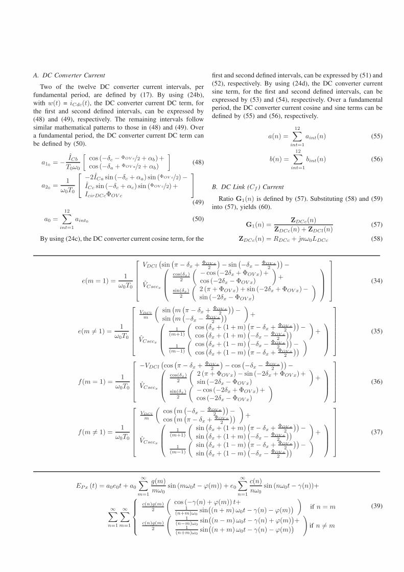
voltage with a low enough Total Harmonic Distortion (THD)
so that dedicated AC side filtering equipment is not required
[9], [12], [13]. The overall efficiency of a HVDC-MMC station
is approximately 99% [14].
This paper focuses on the Alternate Arm Converter (AAC),
which is a type of modular multilevel VSC that has been
proposed for HVDC transmission applications. The AAC was
developed in order to provide a number of advantages over
its predecessor – the MMC – such as improved attributes for
handling DC side faults and requiring fewer sub-modules with
a smaller capacitance [15]–[19]. The AAC was first published
in 2010 [20] and was then initially discussed further in [21],
relating to the original “short-overlap” mode of operation
(“overlap” state angular duration of typically 15-18). To date,
the AAC is yet to seek a commercial application because the
research and development phase is still ongoing. A 20 MW
AAC simulation model was reported to have an efficiency of
98.85% in [22].
In [17], [18], the sizing of the sub-module capacitors
in the AAC and MMC were compared by analyses and
then validated by simulations. In order to have a continuous
analytical AAC model, without requiring Fourier analysis,
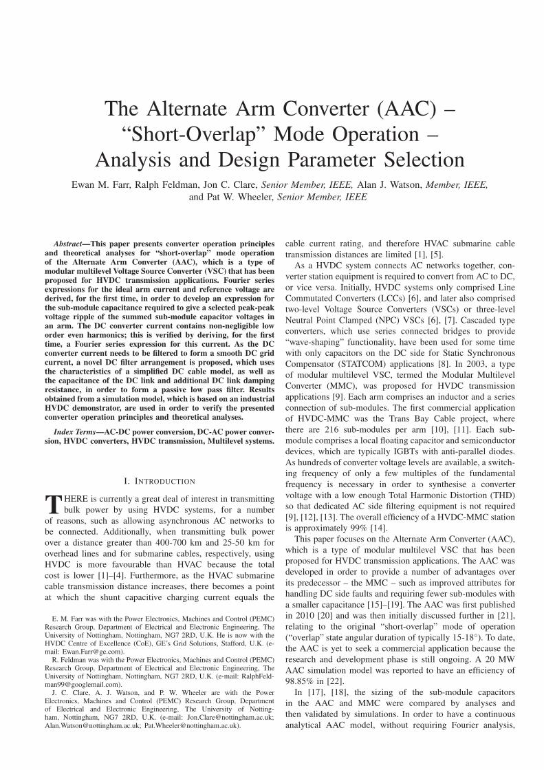
Fig. 1. Alternate Arm Converter (AAC) schematic
each arm was assumed to conduct the entire AC converter
current for half a fundamental period. In fact, during the
two “overlap” states per fundamental period, each arm in a
phase-leg conducts half the AC converter current, as well as
a DC side circulating current. The results revealed that the
AAC sub-module capacitance can be approximately half that
of the MMC in order to give the same maximum peak-peak
sub-module capacitor voltage deviation, around the real and
reactive power operation envelope. This is beneficial because
the physical size and weight of a sub-module is dominated by
the sub-module capacitor [20]. Additionally, when compared
to an equivalently rated MMC, the number of sub-modules
required by the AAC is typically between 30-40% fewer [19].
In previous work for “short-overlap” mode operation [15],
[16], [22]–[24], the DC link capacitor, and a parallel connected
inductor and resistor located between the DC link and the
external DC connection, were used in order to form a smooth
DC grid current, from a DC converter current which contains
non-negligible low order even harmonics. This DC filter
arrangement has the advantage of being ideally lossless, due
to the resistor being connected in parallel with the inductor.
However, when a HVDC link is connected to the DC filter, as
opposed to being connected to a stiff DC voltage source, the
characteristics of the HVDC link will dominate the DC filter
characteristics.
An alternative “extended-overlap” mode of operation for
the AAC was proposed in [25], [26] and was utilised in
[27]. By using an “overlap” state angular duration of 60,
a continuous DC current conduction path is available, with
respect to the DC side. This benefits the AAC by ideally
eliminating the DC converter current ripple, thereby easing
DC side filtering requirements. When operating with only
a fundamental secondary-side converter voltage component,
extending the “overlap” state duration increases the required
voltage rating of the series connection of sub-modules in each
arm. As the nominal sub-module capacitor voltage is usually
already limited by the capacitor and semiconductor device
voltage ratings, increasing the number of sub-modules per arm
negatively impacts the cost and efficiency of the converter.
However, adding a zero sequence component to the secondary-
side converter voltages, which is not present on the primary-
side due to using a wye-delta transformer, reduces the required
voltage rating of the series connection of sub-modules in each
arm by “flattening” the secondary-side converter voltage zero-
crossings, at the expense of increased secondary-side AC to
ground voltage stress and increased director switch voltage
rating, when compared to an AAC operating in the “short-
overlap” mode [19]. The number of sub-modules required for
“extended-overlap” operation with zero sequence injection is
ideally equal to that for “short-overlap” operation without zero
sequence injection, whereas the director switch voltage rating
is 59% higher for “extended-overlap” operation [19]. Note
that, the zero sequence voltages which are typically applied
in “extended-overlap” mode or in conventional VSCs have
the effect of “flattening” the secondary-side converter voltage
zero-crossings or the peaks and troughs, respectively [19],
[28]. However, their purpose is the same – the maximum
fundamental converter voltage which can be synthesised is
increased, for given ratings.
This paper presents a detailed analysis of the AAC in “short-
overlap” mode operation so that the selection of key design
parameters can be made. The considered parameters are the
sub-module capacitance and the parameters of a novel DC
side filter arrangement (noting that the DC side filter is an
important consideration for “short-overlap” mode operation).
The analytical approach taken to derive a continuous expres-
sion for the summed sub-module capacitor energy in an arm,
in order to then find the sub-module capacitance required for
a selected peak-peak voltage ripple, also lends itself well to
deriving a continuous expression for the DC converter current,
which is then used to design and analyse the proposed DC side
filter arrangement.
The remainder of this paper is organised as follows. In
Section II, the AAC topology is described and converter
operation, for the case when operating without zero sequence
voltage injection in the “short-overlap” mode, is explained.
The Conseil International des Grands Reseaux Electriques
(CIGRE) DC grid test system is summarised in Section III
in order to justify the selection of the relevant parameters
and test cases. By deriving, for the first time, Fourier series
expressions for the ideal arm current and reference voltage,
an expression for the sub-module capacitance required to
give a selected peak-peak voltage ripple of the summed sub-
module capacitor voltages in an arm is developed in Section
IV. In Section V, a Fourier series expression for the DC
converter current is derived, for the first time, in order to
verify that this current contains non-negligible low order even
harmonics. Furthermore, as the DC converter current needs
to be filtered in order to form a smooth DC grid current,
a novel DC filter arrangement is proposed, where a passive
low pass filter is formed by the characteristics of a simplified
DC cable model, as well as the capacitance of the DC link
and additional DC link damping resistance. As implementing
a full switching simulation model of the CIGRE DC grid
test system would not have been feasible, a relatively small
scale HVDC demonstrator is described in Section VI, which
is used as the simulation exemplar. The per unit values of the
CIGRE DC grid test system and of the HVDC demonstrator
are equal, where possible. In Section VII, the results obtained
from the AAC simulation model are used in order to validate
the presented converter operation principles and theoretical
analyses. Finally, conclusions are drawn in Section VIII.
II. CONVERTER TOPOLOGY AND OPERATION
The AAC is illustrated in Fig. 1. Each arm comprises an
inductor, a series connection of H-bridge sub-modules and
a director switch. The maximum director switch blocking
voltage, VSWmax, equals VDCl/2 + V refCsecx
− NsmVCAPnom
(see Figs. 2 and 3). In a HVDC system, each director switch
can be formed by a series connection of IGBTs with anti-
parallel diodes so that the required director switch blocking
voltage can be reached.
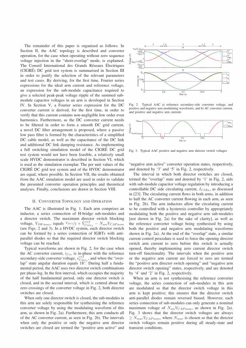
Typical waveforms are shown in Fig. 2, for the case when
the AC converter current, iCx, is in-phase with the reference
secondary-side converter voltage, vrefCsecx, and when the “over-
lap” state angular duration equals 18. During half a funda-
mental period, the AAC uses two director switch combinations
per phase-leg. In the first interval, which occupies the majority
of the half fundamental period, only one director switch is
closed, and in the second interval, which is centred about the
zero crossings of the converter voltage in Fig. 2, both director
switches are closed.
When only one director switch is closed, the sub-modules in
this arm are solely responsible for synthesising the reference
converter voltage by using the modulating waveform of this
arm, as shown in Fig. 2a). Furthermore, this arm conducts all
of the AC converter current, as seen in Fig. 2b). The intervals
when only the positive or only the negative arm director
switches are closed are termed the “positive arm active” and
vCsec
ref
vSMp
ref
vSMn
ref
iCx
iPx
iNx
0 T/4 T/2 3T/4 T
a)
b)
VDCl 2/+
-
NsmVCAPnom
+ CsecrefV
VDCl 2/
CsecrefV-
0
Time (s)
Volt
age
(V)
0
ICx+
ICx-
Curr
ent
(A)
x
x
x
1 1
ICIRx
VDCl 2/ CsecrefV-
x
x
x
3 35 24
Fig. 2. Typical AAC a) reference secondary-side converter voltage, andpositive and negative arm modulating waveforms, and b) AC converter current,and positive and negative arm currents
vSWp
vSWn
x
x
0 T/4 T/2 3T/4 T
Time (s)
Vo
lta
ge
(V)
VCAPnomNmar
0
VSWmax
Fig. 3. Typical AAC positive and negative arm director switch voltages
“negative arm active” converter operation states, respectively,
and denoted by ‘3’ and ‘5’ in Fig. 2, respectively.
The interval in which both director switches are closed,
termed the “overlap” state and denoted by ‘1’ in Fig. 2, aids
with sub-module capacitor voltage regulation by introducing a
controllable DC side circulating current, ICIRx, as discussed
in [23]. The circulating current flows in both arms, in addition
to half the AC converter current flowing in each arm, as seen
in Fig. 2b). The arm inductors allow the circulating current
to be controlled with a hysteresis controller by appropriately
modulating both the positive and negative arm sub-modules
[not shown in Fig. 2a) for the sake of clarity], as well as
the reference converter voltage being synthesised by using
both the positive and negative arm modulating waveforms
shown in Fig. 2a). At the end of the “overlap” state, a similar
current control procedure is used to force the opening director
switch arm current to zero before this switch is actually
opened, thereby implementing zero current director switch
turn-off functionality. The intervals when the positive arm
or the negative arm current are forced to zero are termed
the “positive arm director switch opening” and “negative arm
director switch opening” states, respectively, and are denoted
by ‘4’ and ‘2’ in Fig. 2, respectively.
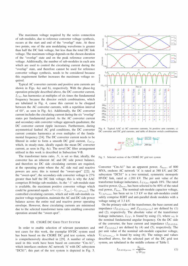
When an arm is not synthesising the reference converter
voltage, the series connection of sub-modules in this arm
are modulated so that the director switch voltage in this
arm is kept positive; this ensures that the director switch
anti-parallel diodes remain reversed biased. However, each
series connection of sub-modules can only generate a nominal
maximum voltage of NsmVCAPnom, as shown in Fig. 2a).
Fig. 3 shows that the director switch voltages are always
≥ NmarVCAPnom, where Nmar is chosen so that the director
switch voltages remain positive during all steady-state and
transient conditions.
The maximum voltage required by the series connection
of sub-modules, due to reference converter voltage synthesis,
occurs at the start and end of the “overlap” state. At these
two points, one of the arm modulating waveforms is greater
than half the DC link voltage, but less than the total DC link
voltage. The maximum voltage depends on the chosen duration
of the “overlap” state and on the peak reference converter
voltage. Additionally, the number of sub-modules in each arm
which are used to control the circulating current during the
“overlap” state, and therefore cannot be used for reference
converter voltage synthesis, needs to be considered because
this requirement further increases the maximum voltage re-
quired.
Typical AC converter currents and positive arm currents are
shown in Figs. 4a) and b), respectively. With the phase-leg
operation principle described above, the DC converter current,
ICdc, has harmonics at multiples of six times the fundamental
frequency because the director switch combinations, which
are tabulated in Fig. 4, cause this current to be chopped
between the AC converter currents, with a repetition interval
of 60, as seen in Fig. 4c). Additionally, the DC converter
current includes the circulating current during the six “overlap”
states per fundamental period. As the AC converter current
and secondary-side converter voltage approach quadrature, the
DC converter current ripple increases. Furthermore, during
asymmetrical faulted AC grid conditions, the DC converter
current contains harmonics at even multiples of the funda-
mental frequency [24]. The DC converter current needs to be
filtered in order to form a smooth DC grid current, IDCg,
which, in steady-state, ideally equals the mean DC converter
current, as seen in Fig. 4c). The novel DC filter arrangement
utilised in this work is described in Subsection V-B.
The transformer turns ratio, N , is set so that, ideally, the
converter has an inherent AC and DC side power balance,
and therefore no DC side circulating currents are required,
at the operating point where the AC side real and reactive
powers are zero; this is termed the “sweet-spot” [22]. At
the “sweet-spot”, the secondary-side converter voltage is 27%
greater than half the DC link voltage; this is why the AAC
comprises H-bridge sub-modules. As the ‘-1’ sub-module state
is available, the maximum positive converter voltage which
could be generated equals +VDCl/2−Nsm (−VCAPnom). The
controlled circulating currents, which aid with sub-module ca-
pacitor voltage regulation, maintain the AC and DC side power
balance across the entire real and reactive power operating
envelope. However, these circulating currents are minimised
due to the selected transformer turns ratio enabling converter
operation around the “sweet-spot”.
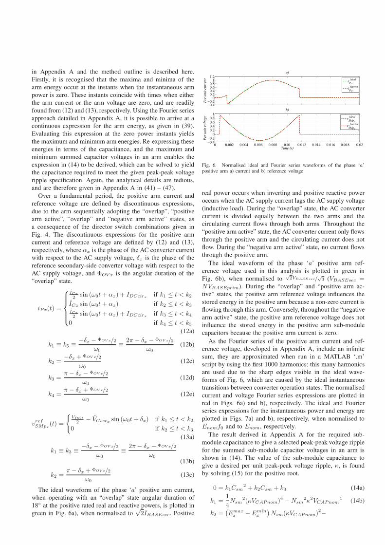
III. CIGRE DC GRID TEST SYSTEM
In order to enable selection of relevant parameters and
test cases for this work, the exemplar HVDC system used
has been based on the CIGRE DC grid test system, which
is comprehensively described in [29]. A number of ratings
used in this work have been based on converter “Cm-A1”,
which interfaces onshore AC network ‘A’ with DC subsystem
“DCS1”; this part of the test system is depicted in Fig. 5.
Fig. 4. Typical AAC a) AC converter currents, b) positive arm currents, c)DC converter and DC grid currents, and table of director switch combinations
Fig. 5. Selected section of the CIGRE DC grid test system
Converter “Cm-A1” has an apparent power, Sbase, of 800
MVA, onshore AC network ‘A’ is rated at 380 kV, and DC
subsystem “DCS1” is a two terminal, symmetric monopole
HVDC link, rated at ±200 kV. The per unit value of the
transformer leakage inductance, LTFpu, equals 18%. The rated
reactive power, Qbase, has been selected to be 40% of the rated
real power, Pbase. The nominal sub-module capacitor voltage,
VCAPnom, has been set to 1.5 kV so that sub-modules could
safely comprise IGBT and anti-parallel diode modules with a
voltage rating of 3.3 kV.
On the primary-side of the transformer, the base current and
impedance (IBASEprim and ZBASEprim) are defined by (1)
and (2), respectively. The absolute value of the transformer
leakage inductance, LTF , is found by using (3), where ω0 is
the nominal fundamental angular frequency. On the DC side
of the converter, the base current and impedance (IBASEdc
and ZBASEdc) are defined by (4) and (5), respectively. The
per unit value of the nominal sub-module capacitor voltage,
VCAPnompu, is found by using (6). The ratings and values
described above, for the selected part of the DC grid test
system, are tabulated in the middle column of Table I.
IBASEprim =Sbase√3VSll
(1)
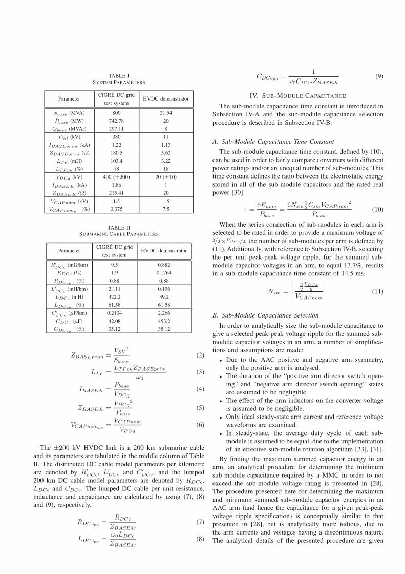
TABLE ISYSTEM PARAMETERS
ParameterCIGRE DC grid
HVDC demonstratortest system
Sbase (MVA) 800 21.54
Pbase (MW) 742.78 20
Qbase (MVAr) 297.11 8
VSll (kV) 380 11
IBASEprim (kA) 1.22 1.13
ZBASEprim (Ω) 180.5 5.62
LTF (mH) 103.4 3.22
LTFpu (%) 18 18
VDCg (kV) 400 (±200) 20 (±10)
IBASEdc (kA) 1.86 1
ZBASEdc (Ω) 215.41 20
VCAPnom (kV) 1.5 1.5
VCAPnompu (%) 0.375 7.5
TABLE IISUBMARINE CABLE PARAMETERS
ParameterCIGRE DC grid
HVDC demonstratortest system
R′
DCc(mΩ/km) 9.5 0.882
RDCc (Ω) 1.9 0.1764
RDCcpu (%) 0.88 0.88
L′
DCc (mH/km) 2.111 0.196
LDCc (mH) 422.2 39.2
LDCcpu (%) 61.58 61.58
C′
DCc(µF/km) 0.2104 2.266
CDCc (µF) 42.08 453.2
CDCcpu (%) 35.12 35.12
ZBASEprim =VSll
2
Sbase
(2)
LTF =LTFpuZBASEprim
ω0(3)
IBASEdc =Pbase
VDCg
(4)
ZBASEdc =VDCg
2
Pbase
(5)
VCAPnompu=
VCAPnom
VDCg
(6)
The ±200 kV HVDC link is a 200 km submarine cable
and its parameters are tabulated in the middle column of Table
II. The distributed DC cable model parameters per kilometre
are denoted by R′DCc, L′
DCc and C′DCc, and the lumped
200 km DC cable model parameters are denoted by RDCc,
LDCc and CDCc. The lumped DC cable per unit resistance,
inductance and capacitance are calculated by using (7), (8)
and (9), respectively.
RDCcpu =RDCc
ZBASEdc
(7)
LDCcpu =ω0LDCc
ZBASEdc
(8)
CDCcpu =1
ω0CDCcZBASEdc
(9)
IV. SUB-MODULE CAPACITANCE
The sub-module capacitance time constant is introduced in
Subsection IV-A and the sub-module capacitance selection
procedure is described in Subsection IV-B.
A. Sub-Module Capacitance Time Constant
The sub-module capacitance time constant, defined by (10),
can be used in order to fairly compare converters with different
power ratings and/or an unequal number of sub-modules. This
time constant defines the ratio between the electrostatic energy
stored in all of the sub-module capacitors and the rated real
power [30].
τ =6Enom
Pbase
=6Nsm
12CsmVCAPnom
2
Pbase
(10)
When the series connection of sub-modules in each arm is
selected to be rated in order to provide a maximum voltage of3/2×VDCg/2, the number of sub-modules per arm is defined by
(11). Additionally, with reference to Subsection IV-B, selecting
the per unit peak-peak voltage ripple, for the summed sub-
module capacitor voltages in an arm, to equal 13.7%, results
in a sub-module capacitance time constant of 14.5 ms.
Nsm =
⌈32VDCg
2
VCAPnom
⌉
(11)
B. Sub-Module Capacitance Selection
In order to analytically size the sub-module capacitance to
give a selected peak-peak voltage ripple for the summed sub-
module capacitor voltages in an arm, a number of simplifica-
tions and assumptions are made:
• Due to the AAC positive and negative arm symmetry,
only the positive arm is analysed.
• The duration of the “positive arm director switch open-
ing” and “negative arm director switch opening” states
are assumed to be negligible.
• The effect of the arm inductors on the converter voltage
is assumed to be negligible.
• Only ideal steady-state arm current and reference voltage
waveforms are examined.
• In steady-state, the average duty cycle of each sub-
module is assumed to be equal, due to the implementation
of an effective sub-module rotation algorithm [23], [31].
By finding the maximum summed capacitor energy in an
arm, an analytical procedure for determining the minimum
sub-module capacitance required by a MMC in order to not
exceed the sub-module voltage rating is presented in [28].
The procedure presented here for determining the maximum
and minimum summed sub-module capacitor energies in an
AAC arm (and hence the capacitance for a given peak-peak
voltage ripple specification) is conceptually similar to that
presented in [28], but is analytically more tedious, due to
the arm currents and voltages having a discontinuous nature.
The analytical details of the presented procedure are given
in Appendix A and the method outline is described here.
Firstly, it is recognised that the maxima and minima of the
arm energy occur at the instants when the instantaneous arm
power is zero. These instants coincide with times when either
the arm current or the arm voltage are zero, and are readily
found from (12) and (13), respectively. Using the Fourier series
approach detailed in Appendix A, it is possible to arrive at a
continuous expression for the arm energy, as given in (39).
Evaluating this expression at the zero power instants yields
the maximum and minimum arm energies. Re-expressing these
energies in terms of the capacitance, and the maximum and
minimum summed capacitor voltages in an arm enables the
expression in (14) to be derived, which can be solved to yield
the capacitance required to meet the given peak-peak voltage
ripple specification. Again, the analytical details are tedious,
and are therefore given in Appendix A in (41) – (47).
Over a fundamental period, the positive arm current and
reference voltage are defined by discontinuous expressions,
due to the arm sequentially adopting the “overlap”, “positive
arm active”, “overlap” and “negative arm active” states, as
a consequence of the director switch combinations given in
Fig. 4. The discontinuous expressions for the positive arm
current and reference voltage are defined by (12) and (13),
respectively, where αx is the phase of the AC converter current
with respect to the AC supply voltage, δx is the phase of the
reference secondary-side converter voltage with respect to the
AC supply voltage, and ΦOV x is the angular duration of the
“overlap” state.
iPx(t) =
ICx
2 sin (ω0t+ αx) + IDCcirx if k1 ≤ t < k2
ICx sin (ω0t+ αx) if k2 ≤ t < k3ICx
2 sin (ω0t+ αx) + IDCcirx if k3 ≤ t < k4
0 if k4 ≤ t < k5(12a)
k1 ≡ k5 ≡ −δx − ΦOV x/2
ω0≡ 2π − δx − ΦOV x/2
ω0(12b)
k2 =−δx + ΦOV x/2
ω0(12c)
k3 =π − δx − ΦOV x/2
ω0(12d)
k4 =π − δx + ΦOV x/2
ω0(12e)
vrefSMpx(t) =
VDCl
2 − VCsecx sin (ω0t+ δx) if k1 ≤ t < k2
0 if k2 ≤ t < k3(13a)
k1 ≡ k3 ≡ −δx − ΦOV x/2
ω0≡ 2π − δx − ΦOV x/2
ω0(13b)
k2 =π − δx + ΦOV x/2
ω0(13c)
The ideal waveform of the phase ‘a’ positive arm current,
when operating with an “overlap” state angular duration of
18 at the positive rated real and reactive powers, is plotted in
green in Fig. 6a), when normalised to√2IBASEsec. Positive
Fig. 6. Normalised ideal and Fourier series waveforms of the phase ‘a’positive arm a) current and b) reference voltage
real power occurs when inverting and positive reactive power
occurs when the AC supply current lags the AC supply voltage
(inductive load). During the “overlap” state, the AC converter
current is divided equally between the two arms and the
circulating current flows through both arms. Throughout the
“positive arm active” state, the AC converter current only flows
through the positive arm and the circulating current does not
flow. During the “negative arm active” state, no current flows
through the positive arm.
The ideal waveform of the phase ‘a’ positive arm ref-
erence voltage used in this analysis is plotted in green in
Fig. 6b), when normalised to√2VBASEsec/
√3 (VBASEsec =
NVBASEprim). During the “overlap” and “positive arm ac-
tive” states, the positive arm reference voltage influences the
stored energy in the positive arm because a non-zero current is
flowing through this arm. Conversely, throughout the “negative
arm active” state, the positive arm reference voltage does not
influence the stored energy in the positive arm sub-module
capacitors because the positive arm current is zero.
As the Fourier series of the positive arm current and ref-
erence voltage, developed in Appendix A, include an infinite
sum, they are approximated when run in a MATLAB ‘.m’
script by using the first 1000 harmonics; this many harmonics
are used due to the sharp edges visible in the ideal wave-
forms of Fig. 6, which are caused by the ideal instantaneous
transitions between converter operation states. The normalised
current and voltage Fourier series expressions are plotted in
red in Figs. 6a) and b), respectively. The ideal and Fourier
series expressions for the instantaneous power and energy are
plotted in Figs. 7a) and b), respectively, when normalised to
Enomf0 and to Enom, respectively.
The result derived in Appendix A for the required sub-
module capacitance to give a selected peak-peak voltage ripple
for the summed sub-module capacitor voltages in an arm is
shown in (14). The value of the sub-module capacitance to
give a desired per unit peak-peak voltage ripple, κ, is found
by solving (15) for the positive root.
0 = k1Csm2 + k2Csm + k3 (14a)
k1 =1
4Nsm
2(κVCAPnom)4 −Nsm
2κ2VCAPnom4 (14b)
k2 =(Emax
x − Eminx
)Nsm(κVCAPnom)
2−
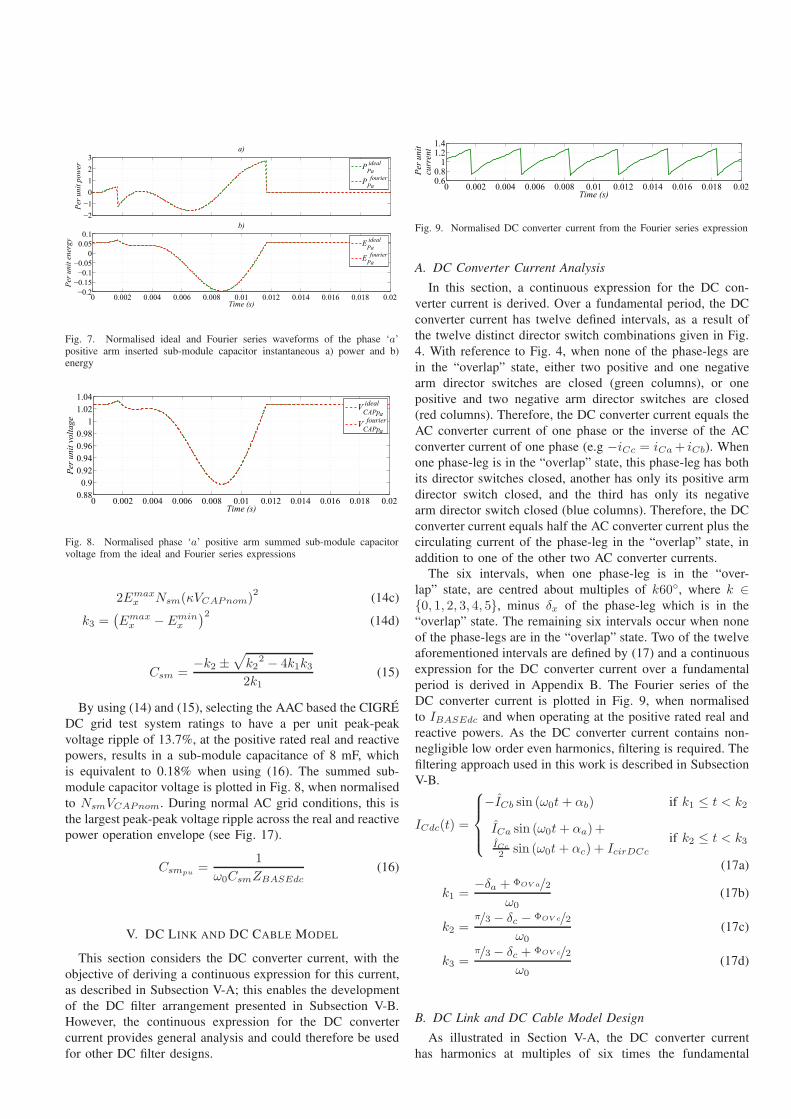
Fig. 7. Normalised ideal and Fourier series waveforms of the phase ‘a’positive arm inserted sub-module capacitor instantaneous a) power and b)energy
Fig. 8. Normalised phase ‘a’ positive arm summed sub-module capacitorvoltage from the ideal and Fourier series expressions
2Emaxx Nsm(κVCAPnom)
2(14c)
k3 =(Emax
x − Eminx
)2(14d)
Csm =−k2 ±
√
k22 − 4k1k3
2k1(15)
By using (14) and (15), selecting the AAC based the CIGRE
DC grid test system ratings to have a per unit peak-peak
voltage ripple of 13.7%, at the positive rated real and reactive
powers, results in a sub-module capacitance of 8 mF, which
is equivalent to 0.18% when using (16). The summed sub-
module capacitor voltage is plotted in Fig. 8, when normalised
to NsmVCAPnom. During normal AC grid conditions, this is
the largest peak-peak voltage ripple across the real and reactive
power operation envelope (see Fig. 17).
Csmpu=
1
ω0CsmZBASEdc
(16)
V. DC LINK AND DC CABLE MODEL
This section considers the DC converter current, with the
objective of deriving a continuous expression for this current,
as described in Subsection V-A; this enables the development
of the DC filter arrangement presented in Subsection V-B.
However, the continuous expression for the DC converter
current provides general analysis and could therefore be used
for other DC filter designs.
Fig. 9. Normalised DC converter current from the Fourier series expression
A. DC Converter Current Analysis
In this section, a continuous expression for the DC con-
verter current is derived. Over a fundamental period, the DC
converter current has twelve defined intervals, as a result of
the twelve distinct director switch combinations given in Fig.
4. With reference to Fig. 4, when none of the phase-legs are
in the “overlap” state, either two positive and one negative
arm director switches are closed (green columns), or one
positive and two negative arm director switches are closed
(red columns). Therefore, the DC converter current equals the
AC converter current of one phase or the inverse of the AC
converter current of one phase (e.g −iCc = iCa+ iCb). When
one phase-leg is in the “overlap” state, this phase-leg has both
its director switches closed, another has only its positive arm
director switch closed, and the third has only its negative
arm director switch closed (blue columns). Therefore, the DC
converter current equals half the AC converter current plus the
circulating current of the phase-leg in the “overlap” state, in
addition to one of the other two AC converter currents.
The six intervals, when one phase-leg is in the “over-
lap” state, are centred about multiples of k60, where k ∈0, 1, 2, 3, 4, 5, minus δx of the phase-leg which is in the
“overlap” state. The remaining six intervals occur when none
of the phase-legs are in the “overlap” state. Two of the twelve
aforementioned intervals are defined by (17) and a continuous
expression for the DC converter current over a fundamental
period is derived in Appendix B. The Fourier series of the
DC converter current is plotted in Fig. 9, when normalised
to IBASEdc and when operating at the positive rated real and
reactive powers. As the DC converter current contains non-
negligible low order even harmonics, filtering is required. The
filtering approach used in this work is described in Subsection
V-B.
ICdc(t) =
−ICb sin (ω0t+ αb) if k1 ≤ t < k2
ICa sin (ω0t+ αa)+ICc
2 sin (ω0t+ αc) + IcirDCc
if k2 ≤ t < k3
(17a)
k1 =−δa + ΦOV a/2
ω0(17b)
k2 =π/3 − δc − ΦOV c/2
ω0(17c)
k3 =π/3 − δc + ΦOV c/2
ω0(17d)
B. DC Link and DC Cable Model Design
As illustrated in Section V-A, the DC converter current
has harmonics at multiples of six times the fundamental
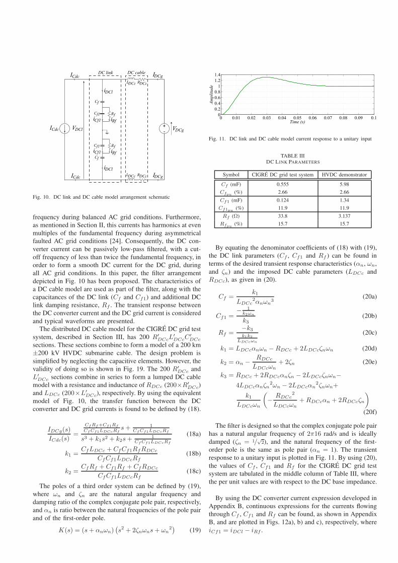
Fig. 10. DC link and DC cable model arrangement schematic
frequency during balanced AC grid conditions. Furthermore,
as mentioned in Section II, this currents has harmonics at even
multiples of the fundamental frequency during asymmetrical
faulted AC grid conditions [24]. Consequently, the DC con-
verter current can be passively low-pass filtered, with a cut-
off frequency of less than twice the fundamental frequency, in
order to form a smooth DC current for the DC grid, during
all AC grid conditions. In this paper, the filter arrangement
depicted in Fig. 10 has been proposed. The characteristics of
a DC cable model are used as part of the filter, along with the
capacitances of the DC link (Cf and Cf1) and additional DC
link damping resistance, Rf . The transient response between
the DC converter current and the DC grid current is considered
and typical waveforms are presented.
The distributed DC cable model for the CIGRE DC grid test
system, described in Section III, has 200 R′DCcL
′DCcC
′DCc
sections. These sections combine to form a model of a 200 km
±200 kV HVDC submarine cable. The design problem is
simplified by neglecting the capacitive elements. However, the
validity of doing so is shown in Fig. 19. The 200 R′DCc and
L′DCc sections combine in series to form a lumped DC cable
model with a resistance and inductance of RDCc (200×R′DCc)
and LDCc (200×L′DCc), respectively. By using the equivalent
model of Fig. 10, the transfer function between the DC
converter and DC grid currents is found to be defined by (18).
IDCg(s)
ICdc(s)=
CfRf+Cf1Rf
CfCf1LDCcRfs+ 1
CfCf1LDCcRf
s3 + k1s2 + k2s+1
CfCf1LDCcRf
(18a)
k1 =CfLDCc + CfCf1RfRDCc
CfCf1LDCcRf
(18b)
k2 =CfRf + Cf1Rf + CfRDCc
CfCf1LDCcRf
(18c)
The poles of a third order system can be defined by (19),
where ωn and ζn are the natural angular frequency and
damping ratio of the complex conjugate pole pair, respectively,
and αn is ratio between the natural frequencies of the pole pair
and of the first-order pole.
K(s) = (s+ αnωn)(s2 + 2ζnωns+ ωn
2)
(19)
Fig. 11. DC link and DC cable model current response to a unitary input
TABLE IIIDC LINK PARAMETERS
Symbol CIGRE DC grid test system HVDC demonstrator
Cf (mF) 0.555 5.98
Cfpu (%) 2.66 2.66
Cf1 (mF) 0.124 1.34
Cf1pu (%) 11.9 11.9
Rf (Ω) 33.8 3.137
Rfpu (%) 15.7 15.7
By equating the denominator coefficients of (18) with (19),
the DC link parameters (Cf , Cf1 and Rf ) can be found in
terms of the desired transient response characteristics (αn, ωn,
and ζn) and the imposed DC cable parameters (LDCc and
RDCc), as given in (20).
Cf =k1
LDCc2αnωn
3(20a)
Cf1 =− 1
k2ωn
k3(20b)
Rf =−k3k1k2
LDCcωn
(20c)
k1 = LDCcαnωn −RDCc + 2LDCcζnωn (20d)
k2 = αn − RDCc
LDCcωn
+ 2ζn (20e)
k3 = RDCc + 2RDCcαnζn − 2LDCcζnωn−4LDCcαnζn
2ωn − 2LDCcαn2ζnωn+
k1LDCcωn
(
− RDCc2
LDCcωn
+RDCcαn + 2RDCcζn
)
(20f)
The filter is designed so that the complex conjugate pole pair
has a natural angular frequency of 2π16 rad/s and is ideally
damped (ζn = 1/√2), and the natural frequency of the first-
order pole is the same as pole pair (αn = 1). The transient
response to a unitary input is plotted in Fig. 11. By using (20),
the values of Cf , Cf1 and Rf for the CIGRE DC grid test
system are tabulated in the middle column of Table III, where
the per unit values are with respect to the DC base impedance.
By using the DC converter current expression developed in
Appendix B, continuous expressions for the currents flowing
through Cf , Cf1 and Rf can be found, as shown in Appendix
B, and are plotted in Figs. 12a), b) and c), respectively, where
iCf1 = iDCl − iRf .
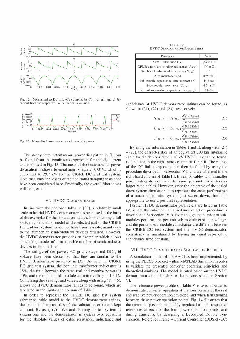
Fig. 12. Normalised a) DC link (Cf ) current, b) Cf1 current, and c) Rf
current from the respective Fourier series expressions
Fig. 13. Normalised instantaneous and mean Rf power
The steady-state instantaneous power dissipation in Rf can
be found from the continuous expression for the Rf current
and is plotted in Fig. 13. The mean of the instantaneous power
dissipation is shown to equal approximately 0.004%, which is
equivalent to 29.7 kW for the CIGRE DC grid test system.
Note that, only the losses of the additional damping resistance
have been considered here. Practically, the overall filter losses
will be greater.
VI. HVDC DEMONSTRATOR
In line with the approach taken in [32], a relatively small
scale industrial HVDC demonstrator has been used as the basis
of the exemplar for the simulation studies. Implementing a full
switching simulation model of the selected part of the CIGRE
DC grid test system would not have been feasible, mainly due
to the number of semiconductor devices required. However,
the HVDC demonstrator provides an exemplar which allows
a switching model of a manageable number of semiconductor
devices to be simulated.
The ratings of the power, AC grid voltage and DC grid
voltage have been chosen so that they are similar to the
HVDC demonstrator presented in [32]. As with the CIGRE
DC grid test system, the per unit transformer inductance is
18%, the ratio between the rated real and reactive powers is
40%, and the nominal sub-module capacitor voltage is 1.5 kV.
Combining these ratings and values, along with using (1) – (6),
allows the HVDC demonstrator ratings to be found, which are
tabulated in the right-hand column of Table I.
In order to represent the CIGRE DC grid test system
submarine cable model at the HVDC demonstrator ratings,
the per unit characteristics of the submarine cable are kept
constant. By using (7) – (9), and defining the test system as
system one and the demonstrator as system two, equations
for the absolute values of cable resistance, inductance and
TABLE IVHVDC DEMONSTRATOR PARAMETERS
Parameter Value
XFMR turns ratio (N )√3× 1.4
XFMR equivalent winding resistance (RTF ) 100 mΩ
Number of sub-modules per arm (Nsm) 10
Arm inductance (L) 0.25 mH
Sub-module capacitance time constant (τ ) 14.5 ms
Sub-module capacitance (Csm) 4.31 mF
Per unit sub-module capacitance (Csmpu ) 3.69%
capacitance at HVDC demonstrator ratings can be found, as
shown in (21), (22) and (23), respectively.
RDCc2 = RDCc1ZBASEdc2
ZBASEdc1(21)
LDCc2 = LDCc1ZBASEdc2
ZBASEdc1(22)
CDCc2 = CDCc1ZBASEdc1
ZBASEdc2(23)
By using the information in Tables I and II, along with (21)
– (23), the characteristics of an equivalent 200 km submarine
cable for the demonstrator ±10 kV HVDC link can be found,
as tabulated in the right-hand column of Table II. The ratings
of the DC link components can then be found by using the
procedure described in Subsection V-B and are tabulated in the
right-hand column of Table III. In reality, cables with a smaller
power rating do not have the same per unit parameters as
larger rated cables. However, since the objective of the scaled
down system simulation is to represent the exact performance
of a much larger rated system, just scaled down, then it is
appropriate to use a per unit representation.
Further HVDC demonstrator parameters are listed in Table
IV, where the sub-module capacitance selection procedure is
described in Subsection IV-B. Even though the number of sub-
modules per arm, the per unit sub-module capacitor voltage,
and the per unit sub-module capacitance are different between
the CIGRE DC test system and the HVDC demonstrator,
consistency is maintained by having an equal sub-module
capacitance time constant.
VII. HVDC DEMONSTRATOR SIMULATION RESULTS
A simulation model of the AAC has been implemented, by
using the PLECS blockset within MATLAB Simulink, in order
to validate the presented converter operating principles and
theoretical analyses. The model is rated based on the HVDC
demonstrator exemplar, due to the reasons stated in Section
VI.
The reference power profile of Table V is used in order to
demonstrate converter operation at the four corners of the real
and reactive power operation envelope, and when transitioning
between these power operation points. Fig. 14 illustrates that
the measured powers are suitably regulated to their respective
references at each of the four power operation points, and
during transients, by designing a Decoupled Double Syn-
chronous Reference Frame – Current Controller (DDSRF-CC)
TABLE VSIMULATION MODEL REFERENCE POWER PROFILE
Time (s) P ref (MW) Qref (MVAr)
0 – 0.5 +20 -8
0.5 – 0.6 +20 -8 ⇒ +8
0.6 – 1.1 +20 +8
1.1 – 1.3 +20 ⇒ -20 +8
1.3 – 1.8 -20 +8
1.8 – 1.9 -20 +8 ⇒ -8
1.9 – 2.4 -20 -8
Fig. 14. Simulation results of the reference and measured a) real and b)reactive powers
[33], based on an AC side equivalent circuit model [34], [35].
Fig. 15 shows the steady-state AC supply voltages, syn-
thesised secondary-side converter voltages, and AC supply
currents, over one fundamental period, when the reference
real and reactive powers are set to +20 MW and +8 MVAr,
respectively.
The steady-state phase-leg ‘a’ positive and negative arm
currents and series connections of sub-module voltages are
shown in Fig. 16. By inspecting Fig. 16a), the arm currents
can be seen to follow the description given in Section II. When
an arm director switch is closed, the secondary-side converter
voltage is synthesised by the series connection of sub-modules
in this arm, as shown in Fig. 16b).
The circulating current is controlled by using the hysteresis
Fig. 15. Simulation results of the steady-state a) supply voltages, b)synthesised secondary-side converter voltages, and c) supply currents whenP ref = +20 MW and Qref = +8 MVAr
Fig. 16. Simulation results of the steady-state phase-leg ‘a’ positive andnegative arm a) currents and b) series connections of sub-module voltageswhen P ref = +20 MW and Qref = +8 MVAr
Fig. 17. Simulation results of the phase-leg ‘a’ positive and negative armsummed sub-module capacitor voltages
controller discussed in [23]. During “overlap”, at least one
sub-module in each arm is not synthesising the secondary-side
converter voltage. These sub-modules can therefore be used
by the hysteresis controller. Practically, the indices of these
sub-modules are written to FPGA registers, by a DSP, at the
sub-module rotation frequency. During “overlap”, the upper
and lower thresholds for the circulating current controller are
written to FPGA registers, at the DSP sampling frequency. The
FPGA calculates the circuiting current, directly from the A2D
converter registers corresponding to the positive and negative
arm currents, which are triggered at a frequency limited by the
A2D conversion duration. The FPGA executes a state machine
which has the circulating current as an input, along with the
sub-module indices and the controller thresholds. The outputs
are the sub-module states required to keep the circulating
current within its thresholds.
Fig. 17 shows the sum of the positive arm and the sum
of negative arm sub-module capacitor voltages for phase-leg
‘a’, over the reference power profile. The maximum steady-
state peak-peak voltage ripple of the summed sub-module
capacitor voltages in each arm is seen to occur when operating
at the rated positive real and reactive power. During this case,
maximum and minimum voltages are approximately 15.54 kV
and 13.43 kV, respectively, giving a peak-peak voltage ripple
of approximately 14%; this ripple is similar to 13.7% specified
in Subsection IV-B.
Fig. 18 shows the DC converter current, DC grid current,
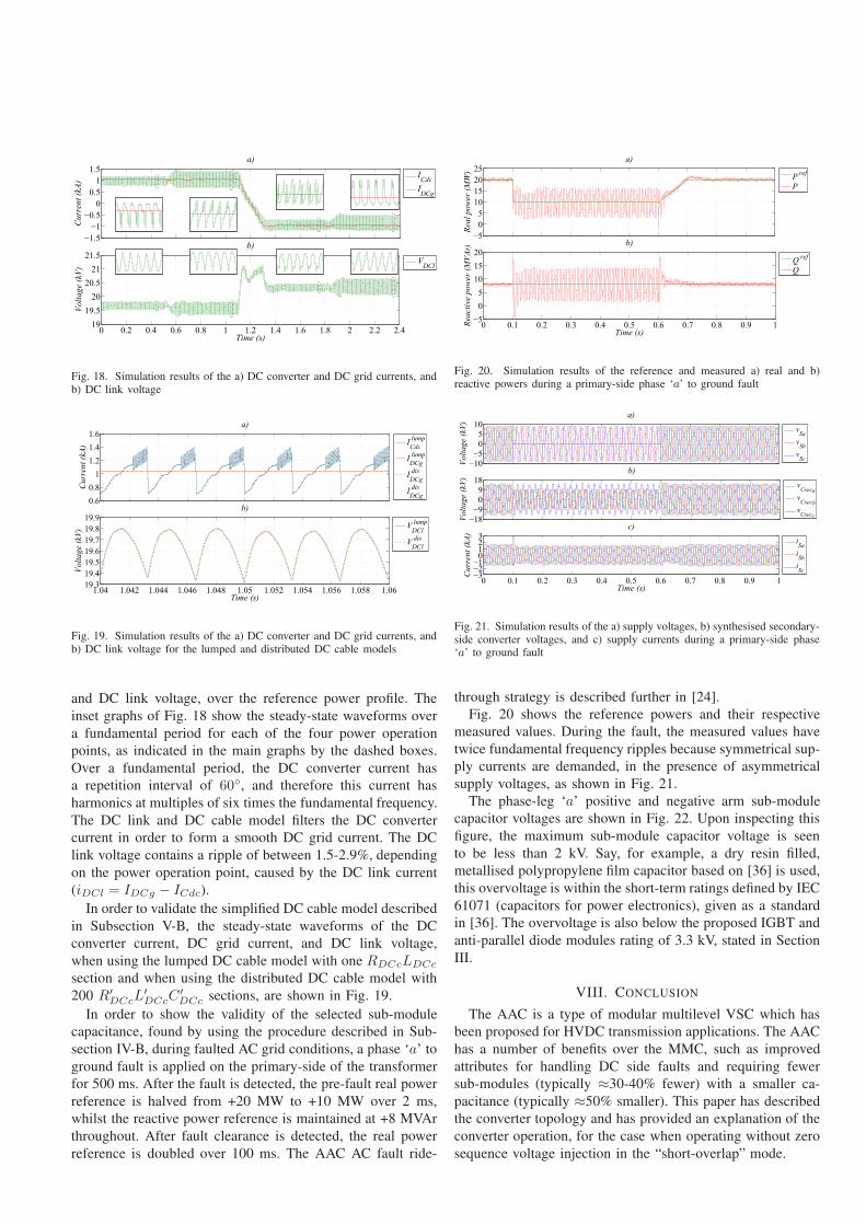
Fig. 18. Simulation results of the a) DC converter and DC grid currents, andb) DC link voltage
Fig. 19. Simulation results of the a) DC converter and DC grid currents, andb) DC link voltage for the lumped and distributed DC cable models
and DC link voltage, over the reference power profile. The
inset graphs of Fig. 18 show the steady-state waveforms over
a fundamental period for each of the four power operation
points, as indicated in the main graphs by the dashed boxes.
Over a fundamental period, the DC converter current has
a repetition interval of 60, and therefore this current has
harmonics at multiples of six times the fundamental frequency.
The DC link and DC cable model filters the DC converter
current in order to form a smooth DC grid current. The DC
link voltage contains a ripple of between 1.5-2.9%, depending
on the power operation point, caused by the DC link current
(iDCl = IDCg − ICdc).
In order to validate the simplified DC cable model described
in Subsection V-B, the steady-state waveforms of the DC
converter current, DC grid current, and DC link voltage,
when using the lumped DC cable model with one RDCcLDCc
section and when using the distributed DC cable model with
200 R′DCcL
′DCcC
′DCc sections, are shown in Fig. 19.
In order to show the validity of the selected sub-module
capacitance, found by using the procedure described in Sub-
section IV-B, during faulted AC grid conditions, a phase ‘a’ to
ground fault is applied on the primary-side of the transformer
for 500 ms. After the fault is detected, the pre-fault real power
reference is halved from +20 MW to +10 MW over 2 ms,
whilst the reactive power reference is maintained at +8 MVAr
throughout. After fault clearance is detected, the real power
reference is doubled over 100 ms. The AAC AC fault ride-
Fig. 20. Simulation results of the reference and measured a) real and b)reactive powers during a primary-side phase ‘a’ to ground fault
Fig. 21. Simulation results of the a) supply voltages, b) synthesised secondary-side converter voltages, and c) supply currents during a primary-side phase‘a’ to ground fault
through strategy is described further in [24].
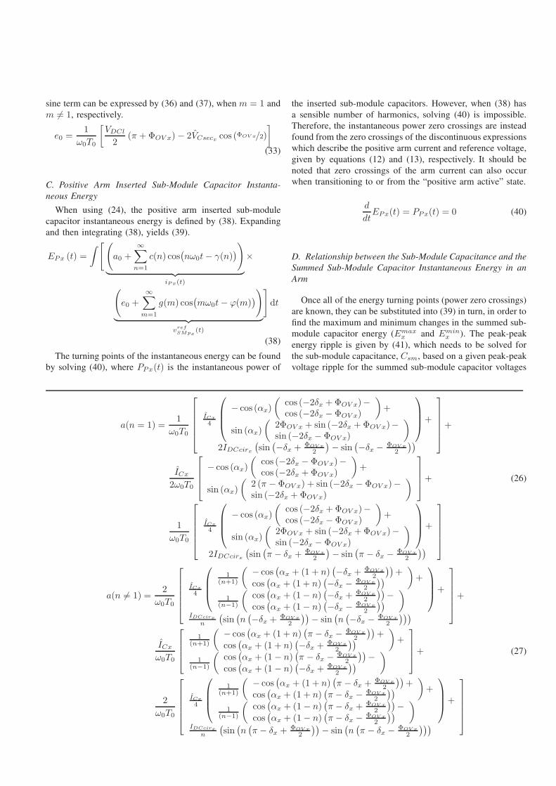
Fig. 20 shows the reference powers and their respective
measured values. During the fault, the measured values have
twice fundamental frequency ripples because symmetrical sup-
ply currents are demanded, in the presence of asymmetrical
supply voltages, as shown in Fig. 21.
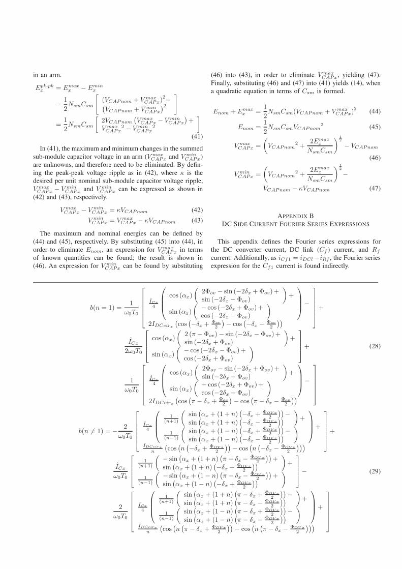
The phase-leg ‘a’ positive and negative arm sub-module
capacitor voltages are shown in Fig. 22. Upon inspecting this
figure, the maximum sub-module capacitor voltage is seen
to be less than 2 kV. Say, for example, a dry resin filled,
metallised polypropylene film capacitor based on [36] is used,
this overvoltage is within the short-term ratings defined by IEC
61071 (capacitors for power electronics), given as a standard
in [36]. The overvoltage is also below the proposed IGBT and
anti-parallel diode modules rating of 3.3 kV, stated in Section
III.
VIII. CONCLUSION
The AAC is a type of modular multilevel VSC which has
been proposed for HVDC transmission applications. The AAC
has a number of benefits over the MMC, such as improved
attributes for handling DC side faults and requiring fewer
sub-modules (typically ≈30-40% fewer) with a smaller ca-
pacitance (typically ≈50% smaller). This paper has described
the converter topology and has provided an explanation of the
converter operation, for the case when operating without zero
sequence voltage injection in the “short-overlap” mode.
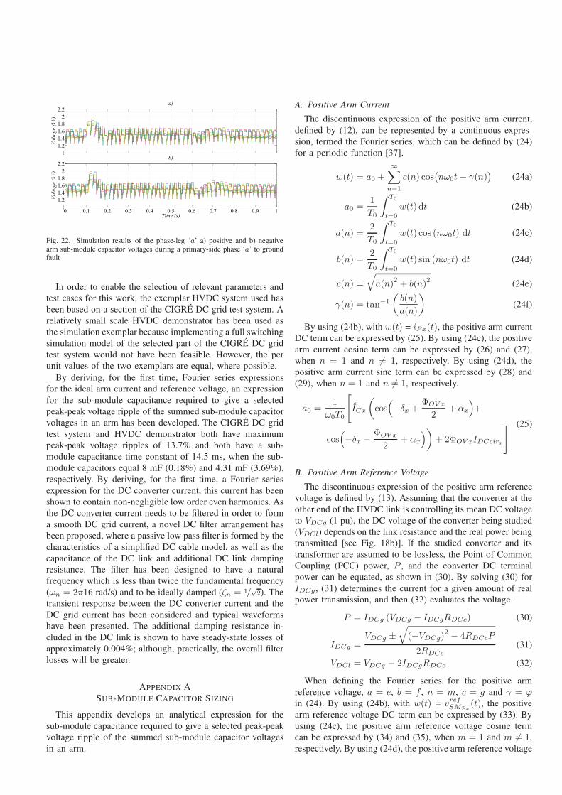
Fig. 22. Simulation results of the phase-leg ‘a’ a) positive and b) negativearm sub-module capacitor voltages during a primary-side phase ‘a’ to groundfault
In order to enable the selection of relevant parameters and
test cases for this work, the exemplar HVDC system used has
been based on a section of the CIGRE DC grid test system. A
relatively small scale HVDC demonstrator has been used as
the simulation exemplar because implementing a full switching
simulation model of the selected part of the CIGRE DC grid
test system would not have been feasible. However, the per
unit values of the two exemplars are equal, where possible.
By deriving, for the first time, Fourier series expressions
for the ideal arm current and reference voltage, an expression
for the sub-module capacitance required to give a selected
peak-peak voltage ripple of the summed sub-module capacitor
voltages in an arm has been developed. The CIGRE DC grid
test system and HVDC demonstrator both have maximum
peak-peak voltage ripples of 13.7% and both have a sub-
module capacitance time constant of 14.5 ms, when the sub-
module capacitors equal 8 mF (0.18%) and 4.31 mF (3.69%),
respectively. By deriving, for the first time, a Fourier series
expression for the DC converter current, this current has been
shown to contain non-negligible low order even harmonics. As
the DC converter current needs to be filtered in order to form
a smooth DC grid current, a novel DC filter arrangement has
been proposed, where a passive low pass filter is formed by the
characteristics of a simplified DC cable model, as well as the
capacitance of the DC link and additional DC link damping
resistance. The filter has been designed to have a natural
frequency which is less than twice the fundamental frequency
(ωn = 2π16 rad/s) and to be ideally damped (ζn = 1/√2). The
transient response between the DC converter current and the
DC grid current has been considered and typical waveforms
have been presented. The additional damping resistance in-
cluded in the DC link is shown to have steady-state losses of
approximately 0.004%; although, practically, the overall filter
losses will be greater.
APPENDIX A
SUB-MODULE CAPACITOR SIZING
This appendix develops an analytical expression for the
sub-module capacitance required to give a selected peak-peak
voltage ripple of the summed sub-module capacitor voltages
in an arm.
A. Positive Arm Current
The discontinuous expression of the positive arm current,
defined by (12), can be represented by a continuous expres-
sion, termed the Fourier series, which can be defined by (24)
for a periodic function [37].
w(t) = a0 +
∞∑
n=1
c(n) cos(nω0t− γ(n)
)(24a)
a0 =1
T0
∫ T0
t=0
w(t) dt (24b)
a(n) =2
T0
∫ T0
t=0
w(t) cos (nω0t) dt (24c)
b(n) =2
T0
∫ T0
t=0
w(t) sin (nω0t) dt (24d)
c(n) =
√
a(n)2 + b(n)2 (24e)
γ(n) = tan−1
(b(n)
a(n)
)
(24f)
By using (24b), with w(t) = iPx(t), the positive arm current
DC term can be expressed by (25). By using (24c), the positive
arm current cosine term can be expressed by (26) and (27),
when n = 1 and n 6= 1, respectively. By using (24d), the
positive arm current sine term can be expressed by (28) and
(29), when n = 1 and n 6= 1, respectively.
a0 =1
ω0T0
[
ICx
(
cos(
−δx +ΦOV x
2+ αx
)
+
cos(
−δx − ΦOV x
2+ αx
))
+ 2ΦOV xIDCcirx
] (25)
B. Positive Arm Reference Voltage
The discontinuous expression of the positive arm reference
voltage is defined by (13). Assuming that the converter at the
other end of the HVDC link is controlling its mean DC voltage
to VDCg (1 pu), the DC voltage of the converter being studied
(VDCl) depends on the link resistance and the real power being
transmitted [see Fig. 18b)]. If the studied converter and its
transformer are assumed to be lossless, the Point of Common
Coupling (PCC) power, P , and the converter DC terminal
power can be equated, as shown in (30). By solving (30) for
IDCg , (31) determines the current for a given amount of real
power transmission, and then (32) evaluates the voltage.
P = IDCg (VDCg − IDCgRDCc) (30)
IDCg =VDCg ±
√
(−VDCg)2 − 4RDCcP
2RDCc
(31)
VDCl = VDCg − 2IDCgRDCc (32)
When defining the Fourier series for the positive arm
reference voltage, a = e, b = f , n = m, c = g and γ = ϕin (24). By using (24b), with w(t) = vrefSMpx
(t), the positive
arm reference voltage DC term can be expressed by (33). By
using (24c), the positive arm reference voltage cosine term
can be expressed by (34) and (35), when m = 1 and m 6= 1,
respectively. By using (24d), the positive arm reference voltage
sine term can be expressed by (36) and (37), when m = 1 and
m 6= 1, respectively.
e0 =1
ω0T0
[VDCl
2(π +ΦOV x)− 2VCsecx cos (ΦOV x/2)
]
(33)
C. Positive Arm Inserted Sub-Module Capacitor Instanta-
neous Energy
When using (24), the positive arm inserted sub-module
capacitor instantaneous energy is defined by (38). Expanding
and then integrating (38), yields (39).
EPx (t) =
∫[(
a0 +
∞∑
n=1
c(n) cos(nω0t− γ(n)
)
)
︸ ︷︷ ︸
iPx(t)
×
(
e0 +
∞∑
m=1
g(m) cos(mω0t− ϕ(m)
)
)
︸ ︷︷ ︸
vref
SMpx(t)
]
dt
(38)
The turning points of the instantaneous energy can be found
by solving (40), where PPx(t) is the instantaneous power of
the inserted sub-module capacitors. However, when (38) has
a sensible number of harmonics, solving (40) is impossible.
Therefore, the instantaneous power zero crossings are instead
found from the zero crossings of the discontinuous expressions
which describe the positive arm current and reference voltage,
given by equations (12) and (13), respectively. It should be
noted that zero crossings of the arm current can also occur
when transitioning to or from the “positive arm active” state.
d
dtEPx(t) = PPx(t) = 0 (40)
D. Relationship between the Sub-Module Capacitance and the
Summed Sub-Module Capacitor Instantaneous Energy in an
Arm
Once all of the energy turning points (power zero crossings)
are known, they can be substituted into (39) in turn, in order to
find the maximum and minimum changes in the summed sub-
module capacitor energy (Emaxx and Emin
x ). The peak-peak
energy ripple is given by (41), which needs to be solved for
the sub-module capacitance, Csm, based on a given peak-peak
voltage ripple for the summed sub-module capacitor voltages
a(n = 1) =1
ω0T0
ICx
4
− cos (αx)
(cos (−2δx +ΦOV x)−cos (−2δx − ΦOV x)
)
+
sin (αx)
(2ΦOV x + sin (−2δx +ΦOV x)−sin (−2δx − ΦOV x)
)
+
2IDCcirx
(sin(−δx + ΦOV x
2
)− sin
(−δx − ΦOV x
2
))
+
ICx
2ω0T0
− cos (αx)
(cos (−2δx − ΦOV x)−cos (−2δx +ΦOV x)
)
+
sin (αx)
(2 (π − ΦOV x) + sin (−2δx − ΦOV x)−sin (−2δx + ΦOV x)
)
+
1
ω0T0
ICx
4
− cos (αx)
(cos (−2δx +ΦOV x)−cos (−2δx − ΦOV x)
)
+
sin (αx)
(2ΦOV x + sin (−2δx +ΦOV x)−sin (−2δx − ΦOV x)
)
+
2IDCcirx
(sin(π − δx + ΦOV x
2
)− sin
(π − δx − ΦOV x
2
))
(26)
a(n 6= 1) =2
ω0T0
ICx
4
1(n+1)
(− cos
(αx + (1 + n)
(−δx + ΦOV x
2
))+
cos(αx + (1 + n)
(−δx − ΦOV x
2
))
)
+
1(n−1)
(cos(αx + (1− n)
(−δx + ΦOV x
2
))−
cos(αx + (1− n)
(−δx − ΦOV x
2
))
)
+
IDCcirx
n
(sin(n(−δx + ΦOV x
2
))− sin
(n(−δx − ΦOV x
2
)))
+
ICx
ω0T0
1(n+1)
(− cos
(αx + (1 + n)
(π − δx − ΦOV x
2
))+
cos(αx + (1 + n)
(−δx + ΦOV x
2
))
)
+
1(n−1)
(cos(αx + (1− n)
(π − δx − ΦOV x
2
))−
cos(αx + (1− n)
(−δx + ΦOV x
2
))
)
+
2
ω0T0
ICx
4
1(n+1)
(− cos
(αx + (1 + n)
(π − δx + ΦOV x
2
))+
cos(αx + (1 + n)
(π − δx − ΦOV x
2
))
)
+
1(n−1)
(cos(αx + (1− n)
(π − δx + ΦOV x
2
))−
cos(αx + (1− n)
(π − δx − ΦOV x
2
))
)
+
IDCcirx
n
(sin(n(π − δx + ΦOV x
2
))− sin
(n(π − δx − ΦOV x
2
)))
(27)
in an arm.
Epk-pkx = Emax
x − Eminx
=1
2NsmCsm
[
(VCAPnom + V maxCAPx)
2−(VCAPnom + V min
CAPx
)2
]
=1
2NsmCsm
[2VCAPnom
(V maxCAPx − V min
CAPx
)+
V maxCAPx
2 − V minCAPx
2
]
(41)
In (41), the maximum and minimum changes in the summed
sub-module capacitor voltage in an arm (VmaxCAPx and V min
CAPx)
are unknowns, and therefore need to be eliminated. By defin-
ing the peak-peak voltage ripple as in (42), where κ is the
desired per unit nominal sub-module capacitor voltage ripple,
V maxCAPx − Vmin
CAPx and V minCAPx can be expressed as shown in
(42) and (43), respectively.
V maxCAPx − V min
CAPx = κVCAPnom (42)
V minCAPx = V max
CAPx − κVCAPnom (43)
The maximum and nominal energies can be defined by
(44) and (45), respectively. By substituting (45) into (44), in
order to eliminate Enom, an expression for V maxCAPx in terms
of known quantities can be found; the result is shown in
(46). An expression for V minCAPx can be found by substituting
(46) into (43), in order to eliminate VmaxCAPx, yielding (47).
Finally, substituting (46) and (47) into (41) yields (14), when
a quadratic equation in terms of Csm is formed.
Enom + Emaxx =
1
2NsmCsm(VCAPnom + V max
CAPx)2
(44)
Enom =1
2NsmCsmVCAPnom
2 (45)
V maxCAPx =
(
VCAPnom2 +
2Emaxx
NsmCsm
) 1
2
− VCAPnom
(46)
V minCAPx =
(
VCAPnom2 +
2Emaxx
NsmCsm
) 1
2
−
VCAPnom − κVCAPnom (47)
APPENDIX B
DC SIDE CURRENT FOURIER SERIES EXPRESSIONS
This appendix defines the Fourier series expressions for
the DC converter current, DC link (Cf ) current, and Rf
current. Additionally, as iCf1 = iDCl− iRf , the Fourier series
expression for the Cf1 current is found indirectly.
b(n = 1) =1
ω0T0
ICx
4
cos (αx)
(2Φov − sin (−2δx +Φov)+sin (−2δx − Φov)
)
+
sin (αx)
(− cos (−2δx +Φov)+cos (−2δx − Φov)
)
−
2IDCcirx
(cos(−δx +
Φov
2
)− cos
(−δx − Φov
2
))
+
ICx
2ω0T0
cos (αx)
(2 (π − Φov)− sin (−2δx − Φov)+sin (−2δx +Φov)
)
+
sin (αx)
(− cos (−2δx − Φov)+cos (−2δx +Φov)
)
+
1
ω0T0
ICx
4
cos (αx)
(2Φov − sin (−2δx +Φov)+sin (−2δx − Φov)
)
+
sin (αx)
(− cos (−2δx +Φov)+cos (−2δx − Φov)
)
−
2IDCcirx
(cos(π − δx + Φov
2
)− cos
(π − δx − Φov
2
))
(28)
b(n 6= 1) = − 2
ω0T0
ICx
4
1(n+1)
(sin(αx + (1 + n)
(−δx + ΦOV x
2
))−
sin(αx + (1 + n)
(−δx − ΦOV x
2
))
)
+
1(n−1)
(sin(αx + (1− n)
(−δx + ΦOV x
2
))−
sin(αx + (1− n)
(−δx − ΦOV x
2
))
)
+
IDCcirx
n
(cos(n(−δx + ΦOV x
2
))− cos
(n(−δx − ΦOV x
2
)))
+
ICx
ω0T0
1(n+1)
(− sin
(αx + (1 + n)
(π − δx − ΦOV x
2
))+
sin(αx + (1 + n)
(−δx + ΦOV x
2
))
)
+
1(n−1)
(− sin
(αx + (1− n)
(π − δx − ΦOV x
2
))+
sin(αx + (1− n)
(−δx + ΦOV x
2
))
)
−
2
ω0T0
ICx
4
1(n+1)
(sin(αx + (1 + n)
(π − δx + ΦOV x
2
))−
sin(αx + (1 + n)
(π − δx − ΦOV x
2
))
)
+
1(n−1)
(sin(αx + (1− n)
(π − δx + ΦOV x
2
))−
sin(αx + (1− n)
(π − δx − ΦOV x
2
))
)
+
IDCcirx
n
(cos(n(π − δx + ΦOV x
2
))− cos
(n(π − δx − ΦOV x
2
)))
(29)
A. DC Converter Current
Two of the twelve DC converter current intervals, per
fundamental period, are defined by (17). By using (24b),
with w(t) = iCdc(t), the DC converter current DC term, for
the first and second defined intervals, can be expressed by
(48) and (49), respectively. The remaining intervals follow
similar mathematical patterns to those in (48) and (49). Over
a fundamental period, the DC converter current DC term can
be defined by (50).
a10 = − ICb
T0ω0
[cos (−δc − ΦOV c/2 + αb)+cos (−δa + ΦOV a/2 + αb)
]
(48)
a20 =1
ω0T0
−2ICa sin (−δc + αa) sin (ΦOV c/2)−ICc sin (−δc + αc) sin (ΦOV c/2)+IcirDCcΦOV c
(49)
a0 =12∑
int=1
aint0 (50)
By using (24c), the DC converter current cosine term, for the
first and second defined intervals, can be expressed by (51) and
(52), respectively. By using (24d), the DC converter current
sine term, for the first and second defined intervals, can be
expressed by (53) and (54), respectively. Over a fundamental
period, the DC converter current cosine and sine terms can be
defined by (55) and (56), respectively.
a(n) =12∑
int=1
aint(n) (55)
b(n) =
12∑
int=1
bint(n) (56)
B. DC Link (Cf ) Current
Ratio G1(n) is defined by (57). Substituting (58) and (59)
into (57), yields (60).
G1(n) =ZDCc(n)
ZDCc(n) + ZDCl(n)(57)
ZDCc(n) = RDCc + nω0LDCc (58)
e(m = 1) =1
ω0T0
VDCl
(sin(π − δx + ΦOV x
2
)− sin
(−δx − ΦOV x
2
))−
VCsecx
cos(δx)2
(− cos (−2δx +ΦOV x)+cos (−2δx − ΦOV x)
)
+
sin(δx)2
(2 (π +ΦOV x) + sin (−2δx +ΦOV x)−sin (−2δx − ΦOV x)
)
(34)
e(m 6= 1) =1
ω0T0
VDCl
m
(sin(m(π − δx + ΦOV x
2
))−
sin(m(−δx − ΦOV x
2
))
)
+
VCsecx
1(m+1)
(cos(δx + (1 +m)
(π − δx + ΦOV x
2
))−
cos(δx + (1 +m)
(−δx − ΦOV x
2
))
)
+
1(m−1)
(cos(δx + (1−m)
(−δx − ΦOV x
2
))−
cos(δx + (1−m)
(π − δx + ΦOV x
2
))
)
(35)
f(m = 1) =1
ω0T0
−VDCl
(cos(π − δx + ΦOV x
2
)− cos
(−δx − ΦOV x
2
))−
VCsecx
cos(δx)2
(2 (π +ΦOV x)− sin (−2δx +ΦOV x)+sin (−2δx − ΦOV x)
)
+
sin(δx)2
(− cos (−2δx +ΦOV x) +cos (−2δx − ΦOV x)
)
(36)
f(m 6= 1) =1
ω0T0
VDCl
m
(cos(m(−δx − ΦOV x
2
))−
cos(m(π − δx + ΦOV x
2
))
)
+
VCsecx
1(m+1)
(sin(δx + (1 +m)
(π − δx + ΦOV x
2
))−
sin(δx + (1 +m)
(−δx − ΦOV x
2
))
)
+
1(m−1)
(sin(δx + (1−m)
(π − δx + ΦOV x
2
))−
sin(δx + (1−m)
(−δx − ΦOV x
2
))
)
(37)
EPx (t) = a0e0t+ a0
∞∑
m=1
g(m)
mω0sin (mω0t− ϕ(m)) + e0
∞∑
n=1
c(n)
nω0sin (nω0t− γ(n))+
∞∑
n=1
∞∑
m=1
c(n)g(m)2
(cos (−γ(n) + ϕ(m)) t+
1(n+m)ω0
sin((n+m)ω0t− γ(n)− ϕ(m)
)
)
if n = m
c(n)g(m)2
(1
(n−m)ω0
sin((n−m)ω0t− γ(n) + ϕ(m)
)+
1(n+m)ω0
sin((n+m)ω0t− γ(n)− ϕ(m)
)
)
if n 6= m
(39)
ZDCl(n) =(CfRf + Cf1Rf ) nω0 + 1
CfCf1Rf (nω0)2+ Cf nω0
(59)
G1(n) =k4(nω0)
3+ k5(nω0)
2+ k6 nω0
k1(nω0)3+ k2(nω0)
2+ k3nω0 + 1
(60a)
k1 = CfCf1LDCcRf (60b)
k2 = CfLDCc + CfCf1RfRDCc (60c)
k3 = CfRf + Cf1Rf + CfRDCc (60d)
k4 = CfCf1LDCcRf (60e)
k5 = CfLDCc + CfCf1RfRDCc (60f)
k6 = CfRDCc (60g)
The DC link current DC term is found by using (61).
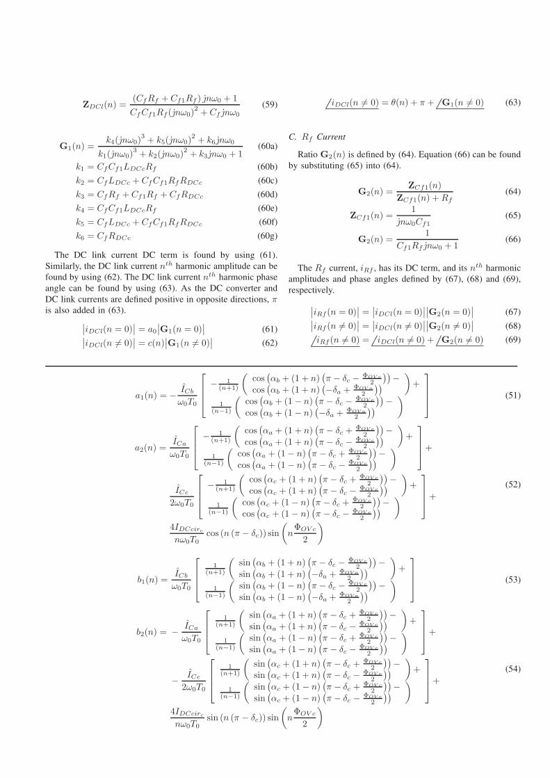
Similarly, the DC link current nth harmonic amplitude can be
found by using (62). The DC link current nth harmonic phase
angle can be found by using (63). As the DC converter and
DC link currents are defined positive in opposite directions, πis also added in (63).
∣∣iDCl(n = 0)
∣∣ = a0
∣∣G1(n = 0)
∣∣ (61)
∣∣iDCl(n 6= 0)
∣∣ = c(n)
∣∣G1(n 6= 0)
∣∣ (62)
iDCl(n 6= 0) = θ(n) + π + G1(n 6= 0) (63)
C. Rf Current
Ratio G2(n) is defined by (64). Equation (66) can be found
by substituting (65) into (64).
G2(n) =ZCf1(n)
ZCf1(n) +Rf
(64)
ZCf1(n) =1
nω0Cf1(65)
G2(n) =1
Cf1Rf nω0 + 1(66)
The Rf current, iRf , has its DC term, and its nth harmonic
amplitudes and phase angles defined by (67), (68) and (69),
respectively.
∣∣iRf (n = 0)
∣∣ =
∣∣iDCl(n = 0)
∣∣∣∣G2(n = 0)
∣∣ (67)
∣∣iRf (n 6= 0)
∣∣ =
∣∣iDCl(n 6= 0)
∣∣∣∣G2(n 6= 0)
∣∣ (68)
iRf (n 6= 0) = iDCl(n 6= 0) + G2(n 6= 0) (69)
a1(n) = − ICb
ω0T0
− 1(n+1)
(cos(αb + (1 + n)
(π − δc − ΦOV c
2
))−
cos(αb + (1 + n)
(−δa +
ΦOV a
2
))
)
+
1(n−1)
(cos(αb + (1− n)
(π − δc − ΦOV c
2
))−
cos(αb + (1− n)
(−δa +
ΦOV a
2
))
)
(51)
a2(n) =ICa
ω0T0
− 1(n+1)
(cos(αa + (1 + n)
(π − δc +
ΦOV c
2
))−
cos(αa + (1 + n)
(π − δc − ΦOV c
2
))
)
+
1(n−1)
(cos(αa + (1− n)
(π − δc +
ΦOV c
2
))−
cos(αa + (1− n)
(π − δc − ΦOV c
2
))
)
+
ICc
2ω0T0
− 1(n+1)
(cos(αc + (1 + n)
(π − δc +
ΦOV c
2
))−
cos(αc + (1 + n)
(π − δc − ΦOV c
2
))
)
+
1(n−1)
(cos(αc + (1− n)
(π − δc +
ΦOV c
2
))−
cos(αc + (1− n)
(π − δc − ΦOV c
2
))
)
+
4IDCcirc
nω0T0cos (n (π − δc)) sin
(
nΦOV c
2
)
(52)
b1(n) =ICb
ω0T0
1(n+1)
(sin(αb + (1 + n)
(π − δc − ΦOV c
2
))−
sin(αb + (1 + n)
(−δa +
ΦOV a
2
))
)
+
1(n−1)
(sin(αb + (1− n)
(π − δc − ΦOV c
2
))−
sin(αb + (1− n)
(−δa +
ΦOV a
2
))
)
(53)
b2(n) = − ICa
ω0T0
1(n+1)
(sin(αa + (1 + n)
(π − δc +
ΦOV c
2
))−
sin(αa + (1 + n)
(π − δc − ΦOV c
2
))
)
+
1(n−1)
(sin(αa + (1− n)
(π − δc +
ΦOV c
2
))−
sin(αa + (1− n)
(π − δc − ΦOV c
2
))
)
+
− ICc
2ω0T0
1(n+1)
(sin(αc + (1 + n)
(π − δc +
ΦOV c
2
))−
sin(αc + (1 + n)
(π − δc − ΦOV c
2
))
)
+
1(n−1)
(sin(αc + (1− n)
(π − δc +
ΦOV c
2
))−
sin(αc + (1− n)
(π − δc − ΦOV c
2
))
)
+
4IDCcirc
nω0T0sin (n (π − δc)) sin
(
nΦOV c
2
)
(54)
ACKNOWLEDGMENT
The authors would like to sincerely thank the HVDC Centre
of Excellence (CoE), GE’s Grid Solutions, Stafford, U.K.
(formerly Alstom Grid) for technical discussions and for the
financial assistance provided towards experimental work. They
would also like to sincerely thank the Center for Power
Electronics Systems (CPES), Virginia Polytechnic Institute
and State University (Virginia Tech), Blacksburg, VA, USA
for their expertise contribution towards this paper.
REFERENCES
[1] J. Arrillaga, Y. H. Liu, and N. R. Watson, Flexible Power Transmission:
The HVDC Options. Wiley-IEEE Press, 2007.[2] V. K. Sood, HVDC and FACTS Controllers: Applications of Static
Converters in Power Systems. Springer, 2004.[3] F. Moreno, M. Merlin, D. Trainer, K. Dyke, and T. Green, “Control
of an alternate arm converter connected to a star transformer,” inPower Electronics and Applications (EPE’14-ECCE Europe), 2014 16th
European Conference on, pp. 1–10, Aug. 2014.[4] C. Kim, V. Sood, G. Jang, S. Lim, and S. Lee, HVDC Transmission:
Power Conversion Applications in Power Systems. Wiley-IEEE Press,2009.
[5] J. Arrillaga, High Voltage Direct Current Transmission. The Institutionof Electrical Engineers, 2nd ed., 1998.
[6] K. Eriksson, “Operational experience of HVDC LightTM ,” in AC-DC
Power Transmission, 2001. Seventh International Conference on (Conf.
Publ. No. 485), pp. 205–210, Nov. 2001.[7] B. Jacobson, Y. Jiang-hfner, P. Rey, G. Asplund, M. Jeroense,
A. Gustafsson, and M. Bergkvist, “HVDC With Voltage Source Con-verters and Extruded Cables for up To ±300 KV and 1000 MW,” inCIGRE, 2009.
[8] J. D. Ainsworth, M. Davies, P. J. Fitz, K. E. Owen, and D. R. Trainer,“Static VAr compensator (STATCOM) based on single-phase chaincircuit converters,” IEE Proceedings - Generation, Transmission and
Distribution, vol. 145, pp. 381–386, Jul. 1998.[9] A. Lesnicar and R. Marquardt, “An innovative modular multilevel
converter topology suitable for a wide power range,” in Power Tech
Conference Proceedings, 2003 IEEE Bologna, vol. 3, pp. 1–6, June2003.
[10] H.-J. Knaak, “Modular multilevel converters and HVDC/FACTS: Asuccess story,” in Power Electronics and Applications (EPE 2011),
Proceedings of the 2011-14th European Conference on, pp. 1–6, Aug.2011.
[11] P. Le-Huy, P. Giroux, and J.-C. Soumagne, “Real-Time Simulation ofModular Multilevel Converters for Network Integration Studies,” inInternational Conference on Power Systems Transients (IPST 2011),June 2011.
[12] J. Rodriguez, J.-S. Lai, and F. Z. Peng, “Multilevel inverters: a surveyof topologies, controls, and applications,” Industrial Electronics, IEEE
Transactions on, vol. 49, pp. 724–738, Aug. 2002.
[13] S. Allebrod, R. Hamerski, and R. Marquardt, “New transformerless,scalable Modular Multilevel Converters for HVDC-transmission,” inPower Electronics Specialists Conference, 2008. PESC 2008. IEEE,pp. 174–179, June 2008.
[14] C. Oates and C. Davidson, “A comparison of two methods of estimatinglosses in the Modular Multi-Level Converter,” in Power Electronics
and Applications (EPE 2011), Proceedings of the 2011-14th European
Conference on, pp. 1–10, Aug. 2011.
[15] R. Feldman, A. Watson, J. Clare, P. Wheeler, D. Trainer, and R. Crookes,“DC fault ride-through capability and statcom operation of a hybridvoltage source converter arrangement for HVDC power transmissionand reactive power compensation,” in Power Electronics, Machines and
Drives (PEMD 2012), 6th IET International Conference on, pp. 1–5,March 2012.
[16] R. Feldman, E. Farr, A. Watson, J. Clare, P. Wheeler, D. Trainer, andR. Crookes, “DC fault ride-through capability and STATCOM operationof a HVDC hybrid voltage source converter,” Generation, Transmission
& Distribution, IET, vol. 8, pp. 114–120, Jan. 2014.
[17] M. Merlin, T. Green, P. Mitcheson, F. Moreno, K. Dyke, and D. Trainer,“Cell capacitor sizing in modular multilevel converters and hybridtopologies,” in Power Electronics and Applications (EPE’14-ECCE
Europe), 2014 16th European Conference on, pp. 1–10, Aug. 2014.
[18] M. Merlin and T. Green, “Cell capacitor sizing in multilevel converters:cases of the modular multilevel converter and alternate arm converter,”Power Electronics, IET, vol. 8, no. 3, pp. 350–360, 2015.
[19] F.J.Moreno, M. Merlin, D. Trainer, T. Green, and K. Dyke, “Zero phasesequence voltage injection for the alternate arm converter,” in AC and
DC Power Transmission, 11th IET International Conference on, pp. 1–6,Feb. 2015.
[20] D. Trainer, C. Davidson, C. Oates, N.M., Macleod, D. Critchley, andR. Crookes, “A New Hybrid Voltage-sourced Converter for HVDCPower Transmission,” in CIGRE, Aug. 2010.
[21] M. Merlin, T. Green, P. Mitcheson, D. Trainer, D. Critchley, andR. Crookes, “A new hybrid multi-level Voltage-Source Converter withDC fault blocking capability,” in AC and DC Power Transmission, 2010.
ACDC. 9th IET International Conference on, pp. 1–5, Oct. 2010.[22] M. Merlin, T. Green, P. Mitcheson, D. Trainer, R. Critchley, W. Crookes,
and F. Hassan, “The Alternate Arm Converter: A New Hybrid MultilevelConverter With DC-Fault Blocking Capability,” Power Delivery, IEEE
Transactions on, vol. 29, pp. 310–317, Feb. 2014.[23] E. Farr, R. Feldman, A. Watson, J. Clare, and P. Wheeler, “A sub-
module capacitor voltage balancing scheme for the Alternate ArmConverter (AAC),” in Power Electronics and Applications (EPE), 2013
15th European Conference on, pp. 1–10, Sept. 2013.[24] E. Farr, R. Feldman, A. Watson, R. Burgos, J. Clare, P. Wheeler, and
D. Boroyevich, “Alternate Arm Converter (AAC) operation under faultedAC-grid conditions,” in Power Electronics, Machines and Drives (PEMD
2014), 7th IET International Conference on, pp. 1–6, April 2014.[25] S. Fekriasl, M. M. C. Merlin, T. C. Green, K. Dyke, F. J. Moreno Munoz,
O. F. Jasim, and B. Masoud, “Improvements in or relating to thecontrol of converters.” http://www.freepatentsonline.com/EP2884653A1.html, June 2015. EP Patent App. EP2884653.
[26] D. Trainer, T. Green, M. Merlin, and D. Soto-Sanchez, “Converter.”https://www.google.com.ar/patents/EP2727234A1?cl=en, May 2014. EPPatent App. EP20,110,728,832.
[27] P. D. Judge, G. Chaffey, P. Clemow, M. M. Merlin, and T. C. Green,“Hardware Testing of the Alternate Arm Converter Operating in itsExtended Overlap Mode,” in International High Voltage Direct Current
2015 Conference (HVDC 2015), Oct. 2015.[28] K. Ilves, S. Norrga, L. Harnefors, and H. P. Nee, “On Energy Storage
Requirements in Modular Multilevel Converters,” IEEE Transactions on
Power Electronics, vol. 29, pp. 77–88, Jan. 2014.[29] T. K. Vrana, S. Dennetiere, Y. Yanga, J. Jardini, D. Jovcic, and H. Saad,
“The CIGRE B4 DC Grid Test System,” CIGRE, Oct. 2013.[30] M. Hagiwara and H. Akagi, “PWM control and experiment of modular
multilevel converters,” in Power Electronics Specialists Conference,
2008. PESC 2008. IEEE, pp. 154–161, June 2008.[31] G. Adam, O. Anaya-Lara, G. Burt, D. Telford, B. Williams, and
J. McDonald, “Modular multilevel inverter: Pulse width modulation andcapacitor balancing technique,” Power Electronics, IET, vol. 3, pp. 702–715, Sept. 2010.
[32] C. C. Davidson, A. C. Lancaster, A. J. Totterdell, and C. D. M. Oates, “A24 MW level voltage source converter demonstrator to evaluate differentconverter topologies,” in CIGRE, 2012.
[33] R. Teodorescu, M. Liserre, and P. Rodriguez, Grid Converters for
Photovoltaic and Wind Power Systems. John Wiley & Sons, Inc., 2011.[34] A. Yazdani and R. Iravani, Voltage-Sourced Converters in Power Sys-
tems: Modeling, Control, and Applications. Wiley-IEEE Press, 2010.[35] J. Wang, E. Farr, R. Burgos, D. Boroyevich, R. Feldman, A. Watson,
J. Clare, and P. Wheeler, “State-space switching model of modularmultilevel converters,” in Control and Modeling for Power Electronics
(COMPEL), 2013 IEEE 14th Workshop on, pp. 1–10, June 2013.[36] Vishay, “Power Electronic Capacitors (PEC) – Rectangular.” http://www.
vishay.com/docs/13020/dcmkprectangular.pdf, 2017. [Online; accessed23-June-2017].
[37] J. W. Nilsson and S. Riedel, Electric Circuits. Prentice Hall, 9th ed.,2010.
Ewan M. Farr received the M.Eng. (Hons.) de-gree and the Ph.D. degree, for his work on theAlternate Arm Converter (AAC), both in electricaland electronic engineering from the University ofNottingham, Nottingham, U.K., in 2011 and 2016,respectively. From 2012 to 2013, he was a VisitingScholar in the Center for Power Electronics Systems(CPES), Virginia Polytechnic Institute and StateUniversity (Virginia Tech), Blacksburg, VA, USA.From 2015 to 2016, he was a Research Fellow in thePower Electronics, Machines and Control (PEMC)
Research Group at the University of Nottingham, Nottingham, U.K. In 2016,he joined the HVDC Centre of Excellence (CoE) at GE’s Grid Solutions,Stafford, U.K., where he is currently an Emerging Technologies Engineerin the Research and Technology Department. His research interests includecontrol and modulation for HVDC converters.
Ralph Feldman received the Ph.D. degree in elec-trical engineering for his work on induction ma-chine standard efficiency tests from the Universityof Nottingham, Nottingham, U.K., in 2007. From2007 to 2016, he worked at the University of Not-tingham, Nottingham, U.K., as a Research Fellowin the Power Electronics, Machines and Control(PEMC) Research Group. His research interests in-clude power-converter topologies and HVDC trans-mission systems.
Jon C. Clare was born in Bristol, U.K., in 1957.He received the B.Sc. and Ph.D. degrees in electricalengineering from the University of Bristol, Bristol,U.K. From 1984 to 1990, he was a Research As-sistant and a Lecturer at the University of Bristol,where he was involved in teaching and researchon power electronic systems. Since 1990, he hasbeen with the Power Electronics, Machines andControl (PEMC) Research Group at the Universityof Nottingham, Nottingham, U.K., where he is cur-rently Professor of Power Electronics and Head of
Research Group. His research interests include power electronic convertertopologies, modulation and control strategies, and power conversion systems.
Alan J. Watson received the M.Eng. (Hons.) de-gree in electronic engineering from the Universityof Nottingham, Nottingham, U.K. in 2004 beforepursuing the Ph.D. degree in Power Electronics,also at the University of Nottingham, Nottingham,U.K. In 2008, he became a Research Fellow in thePower Electronics Machines and Control (PEMC)Research Group, working on the UNIFLEX project(http://www.eee.nott.ac.uk/uniflex/). Since 2008, hehas worked on several projects in the area of highpower electronics including high power resonant
converters, high voltage power supplies, and multilevel converters for gridconnected applications such as HVDC and FACTS. In 2012, he was promotedto Senior Research Fellow before becoming a Lecturer in High PowerElectronics in 2013. His research interests include the development and controlof advanced high power conversion topologies for industrial applications,future energy networks, and VSC-HVDC.
Pat W. Wheeler received the B.Eng. (Hons.) degreein 1990 from the University of Bristol, Bristol,U.K. He received the Ph.D. degree in electricalengineering for his work on matrix converters fromthe University of Bristol, Bristol, U.K. in 1994. In1993, he moved to the University of Nottingham,Nottingham, U.K. and worked as a Research Assis-tant in the Department of Electrical and ElectronicEngineering. In 1996, he became a Lecturer in thePower Electronics, Machines and Control (PEMC)Research Group at the University of Nottingham,
Nottingham, U.K. Since January 2008, he has been a Full Professor in thesame research group. He is currently Head of the Department of Electricaland Electronic Engineering at the University of Nottingham, Nottingham, U.K.He is an IEEE PELs “Member at Large” and an IEEE PELs DistinguishedLecturer. He has published 400 academic publications in leading internationalconferences and journals.
Recommended