10/11/2017
1
LFoundry S.r.l. All rights reserved.
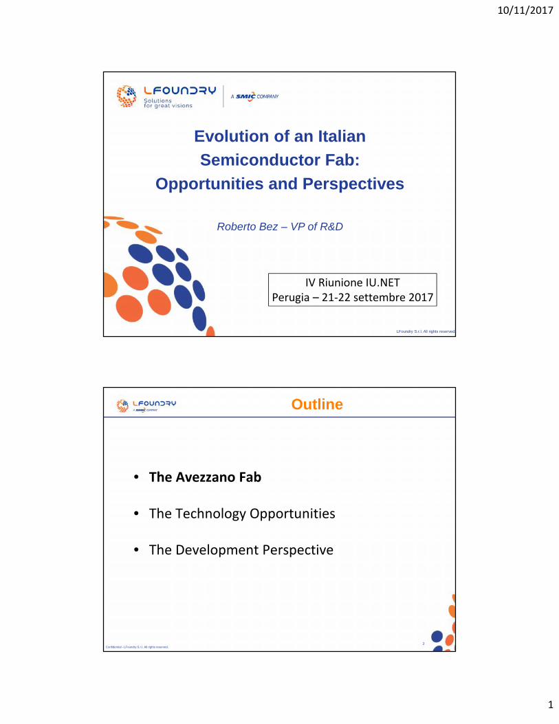
Evolution of an ItalianSemiconductor Fab:
Opportunities and Perspectives
Roberto Bez – VP of R&D
IV Riunione IU.NETPerugia – 21-22 settembre 2017
Confidential - LFoundry S.r.l. All rights reserved.2
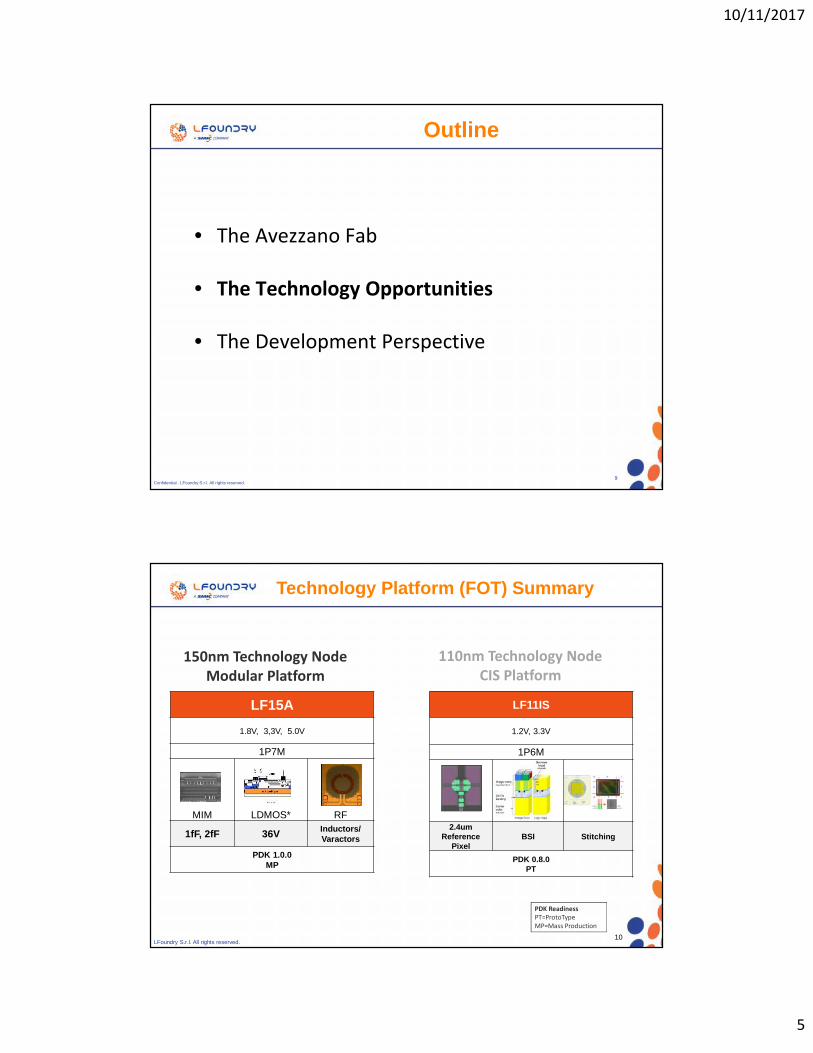
Outline
• The Avezzano Fab
• The Technology Opportunities
• The Development Perspective
10/11/2017
2
LFoundry S.r.l. All rights reserved.3
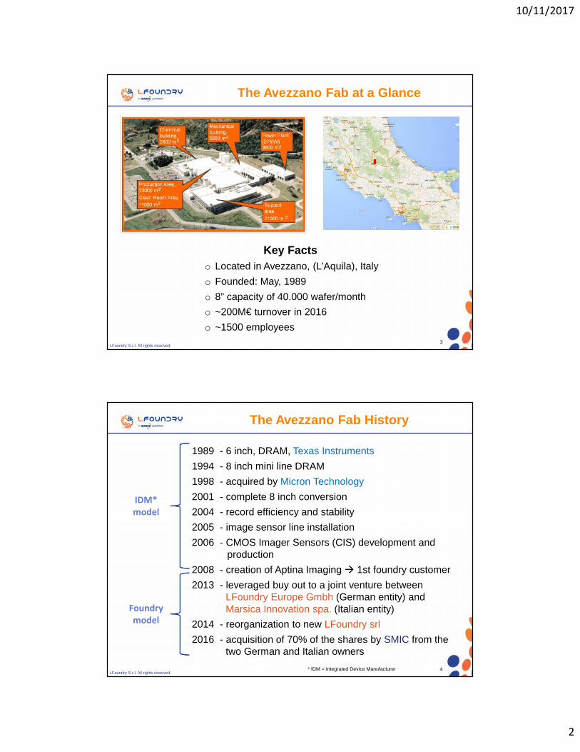
The Avezzano Fab at a Glance
Key Factso Located in Avezzano, (L’Aquila), Italyo Founded: May, 1989o 8” capacity of 40.000 wafer/montho ~200M€ turnover in 2016o ~1500 employees
LFoundry S.r.l. All rights reserved.4
The Avezzano Fab History
1989 - 6 inch, DRAM, Texas Instruments1994 - 8 inch mini line DRAM1998 - acquired by Micron Technology2001 - complete 8 inch conversion2004 - record efficiency and stability2005 - image sensor line installation2006 - CMOS Imager Sensors (CIS) development and
production2008 - creation of Aptina Imaging 1st foundry customer2013 - leveraged buy out to a joint venture between
LFoundry Europe Gmbh (German entity) andMarsica Innovation spa. (Italian entity)
2014 - reorganization to new LFoundry srl2016 - acquisition of 70% of the shares by SMIC from the
two German and Italian owners
IDM*model
Foundrymodel
* IDM = Integrated Device Manufacturer
10/11/2017
3
LFoundry S.r.l. All rights reserved.5
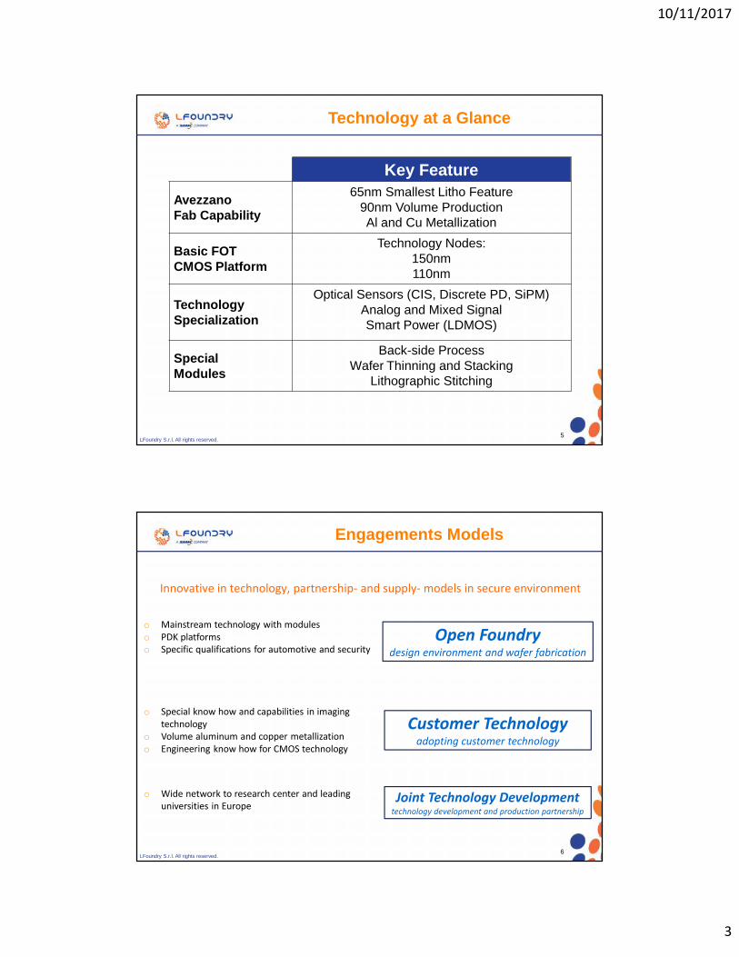
Technology at a Glance
Key FeatureAvezzanoFab Capability
65nm Smallest Litho Feature90nm Volume ProductionAl and Cu Metallization
Basic FOTCMOS Platform
Technology Nodes:150nm110nm
TechnologySpecialization
Optical Sensors (CIS, Discrete PD, SiPM)Analog and Mixed SignalSmart Power (LDMOS)
SpecialModules
Back-side ProcessWafer Thinning and Stacking
Lithographic Stitching
LFoundry S.r.l. All rights reserved.6
Engagements Models
Innovative in technology, partnership- and supply- models in secure environment
o Mainstream technology with moduleso PDK platformso Specific qualifications for automotive and security
o Special know how and capabilities in imagingtechnology
o Volume aluminum and copper metallizationo Engineering know how for CMOS technology
o Wide network to research center and leadinguniversities in Europe
Open Foundrydesign environment and wafer fabrication
Customer Technologyadopting customer technology
Joint Technology Developmenttechnology development and production partnership
10/11/2017
4
LFoundry S.r.l. All rights reserved.7
Foundry Prototyping Services
Flexible Manufacturing options
Full Mask Set• Full flexibility in timing and volume
• Reasonable NRE* cost
MLM (Multi Layer Mask)• Full flexibility in timing for small
volume production
• Significantly reduced NRE costs
MPW (Multi Project Wafer)• Ideal solution for prototyping and
low volume production
• Lowest NRE costs
Full mask
MLM
MPW
* NRE = Not Recurring Engineering
LFoundry S.r.l. All rights reserved.8
Probe & Analytics Service
Full equipped Laboratory for internaland external Failure Analysis7 Days/week, 08-20 shift coverage
Failure Analysis Lab
Focus Ion Beams2 x Dual Beam FEI Strata 235
Scanning Electron Microscopes2 x Hitachi 47001 x Hitachi 4800 (with EDX)2 x FEI Nova-600 Nanosem
Chemical Laboratory (Incoming Quality)
Provide analytical and material competences tomeet products and operations requirements.
Wafer Level Reliability Equipment
… more services available
TEM/STEM:TECNAI G2 F30 S-Twin equipped withLorentz Lens, Bi-prism. EELS andEDX detector. Holography, Tomography
Probe AreaIn House electrical testing enable fast feedbackabout the quality and yield of products7 Days/week, 24h shift coveragePCM (Process control monitor)Memory Tester (DRAM/SRAM)Mixed Signal TesterImager testing
10/11/2017
5
Confidential - LFoundry S.r.l. All rights reserved.9
Outline
• The Avezzano Fab
• The Technology Opportunities
• The Development Perspective
LFoundry S.r.l. All rights reserved.10
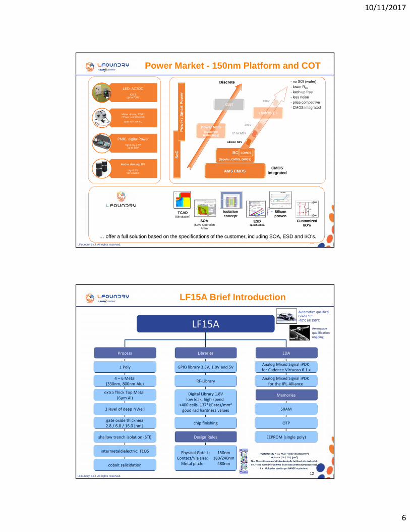
Technology Platform (FOT) Summary
LF11IS
1.2V, 3.3V
1P6M
2.4umReference
PixelBSI Stitching
PDK 0.8.0PT
LF15A1.8V, 3,3V, 5.0V
1P7M
MIM LDMOS* RF
1fF, 2fF 36V Inductors/Varactors
PDK 1.0.0MP
150nm Technology NodeModular Platform
110nm Technology NodeCIS Platform
PDK ReadinessPT=ProtoTypeMP=Mass Production
10/11/2017
6
LFoundry S.r.l. All rights reserved.11
Power Market - 150nm Platform and COT
LED, AC2DCIGBT
up to 700V
Motor driver, POE*(*Power over Ethernet)
up to 80V, low Ron
PMIC, digital PowerVg=3.3V / 5V
up to 80V
Audio, Analog, RF
Vg=3.3Vfull isolation
Discrete
SoC
CMOSintegrated
Power MOS(customer
technology)
IGBT
BCD(Bipolar, CMOS, DMOS)
AMS CMOS
LDMOS
LDMOS 2.0
silicon 60V
1st Si 120V
800V
300V
Pow
er /
Smar
t Pow
er
… offer a full solution based on the specifications of the customer, including SOA, ESD and I/O’s.… offer a full solution based on the specifications of the customer, including SOA, ESD and I/O’s.
TCAD(Simulation)
SOA(Save Operation
Area)
ESDspecification
0 5 10 15 20 250
0.5
1
1.5
2
2.5
3TLP IV
TLP
Cur
rent
(A)
TLP Voltage (V)10-9 10-8 10-7 10-6 10-5 10-4
Leak Current (A)
Spots
gbnld8_w90m15_rgs10k\s1gbnld8_w90m15_rgs20k\s1gbnld8_w90m15_rgs50k\s1gbnld8_w90m15_rgs100k\s1gbnld8_w90m15_rgs200k\s1
0 5 10 15 20 250
0.5
1
1.5
2
2.5
3TLP IV
TLP
Cur
rent
(A)
TLP Voltage (V)10-9 10-8 10-7 10-6 10-5 10-4
Leak Current (A)
Spots
gbnld8_w90m15_rgs10k\s1gbnld8_w90m15_rgs20k\s1gbnld8_w90m15_rgs50k\s1gbnld8_w90m15_rgs100k\s1gbnld8_w90m15_rgs200k\s1
CustomizedI/O’s
Isolationconcept
Siliconproven
- no SOI (wafer)- lower Ron
- latch up free- less noise- price competitive- CMOS integrated
LFoundry S.r.l. All rights reserved.12
LF15A Brief Introduction
* GateDensity = (1 / NCS) * 1000 [kGates/mm²]NCS = 4 x (TA / TTC) [µm²]
TA = The entire area of all standardcells (without physical cells).TTC = The number of all MOS in all cells (without physical cells).
4 x : Multiplier used to get NAND2 equivalent.
Process
LF15ALF15A
Libraries
GPIO library 3.3V, 1.8V and 5VGPIO library 3.3V, 1.8V and 5V
4 – 6 Metal(330nm, 800nm Alu)
4 – 6 Metal(330nm, 800nm Alu)
1 Poly1 Poly
RF-LibraryRF-Library
Digital Library 1.8Vlow leak, high speed
>400 cells, 137*kGates/mm²good rad hardness values
Digital Library 1.8Vlow leak, high speed
>400 cells, 137*kGates/mm²good rad hardness values
intermetaldielectric: TEOSintermetaldielectric: TEOS
cobalt salicidationcobalt salicidation
extra Thick Top Metal(6µm Al)
extra Thick Top Metal(6µm Al)
EDA
2 level of deep NWell2 level of deep NWell
gate oxide thickness2.8 / 6.8 / 16.0 [nm]gate oxide thickness2.8 / 6.8 / 16.0 [nm]
shallow trench isolation (STI)shallow trench isolation (STI)
Analog Mixed Signal iPDKfor Cadence Virtuoso 6.1.xAnalog Mixed Signal iPDKfor Cadence Virtuoso 6.1.x
Analog Mixed Signal iPDKfor the IPL-Alliance
Analog Mixed Signal iPDKfor the IPL-Alliance
OTPOTP
EEPROM (single poly)EEPROM (single poly)
SRAMSRAM
chip finishingchip finishing
Physical Gate L: 150nmContact/Via size: 180/240nm
Metal pitch: 480nm
Physical Gate L: 150nmContact/Via size: 180/240nm
Metal pitch: 480nm
Memories
Design Rules
Automotive qualifiedGrade “0”-40°C till 150°C
Aerospacequalificationongoing
10/11/2017
7
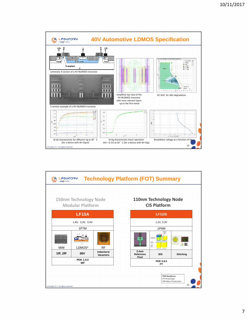
LFoundry S.r.l. All rights reserved.13
40V Automotive LDMOS Specification
schematic X-section of a HV-NLDMOS transistor
X-section example of a HV-NLDMOS transistor
simplified top view of theHV-NLDMOS transistor
with most relevant layersup to the first metal
Id-Vd characteristic for different Vg at 30°C(for a device with W=10µm)
Id-Vg characteristic linear operation(Vd = 0.1V) at 30°C (for a device with W=10µ)
Breakdown voltage as a function of Vg
HC-SOA for Idlin degradation
LFoundry S.r.l. All rights reserved.14
Technology Platform (FOT) Summary
LF11IS
1.2V, 3.3V
1P6M
2.4umReference
PixelBSI Stitching
PDK 0.8.0PT
LF15A1.8V, 3,3V, 5.0V
1P7M
MIM LDMOS* RF
1fF, 2fF 36V Inductors/Varactors
PDK 1.0.0MP
150nm Technology NodeModular Platform
110nm Technology NodeCIS Platform
PDK ReadinessPT=ProtoTypeMP=Mass Production
10/11/2017
8
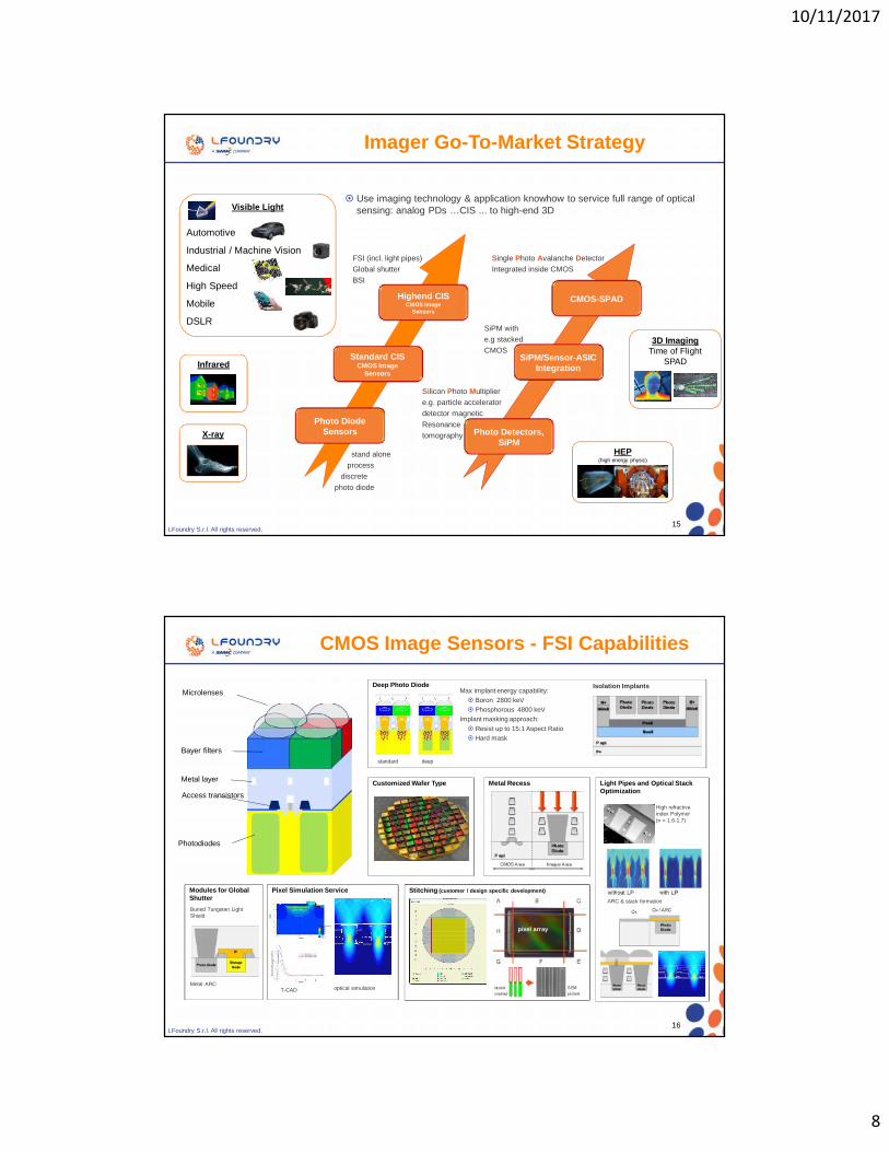
LFoundry S.r.l. All rights reserved.15
Imager Go-To-Market Strategy
InfraredInfrared
Visible Light
Automotive
Industrial / Machine Vision
Medical
High Speed
Mobile
DSLR
Visible Light
Automotive
Industrial / Machine Vision
Medical
High Speed
Mobile
DSLR
X-rayX-rayPhoto Diode
Sensors
Highend CISCMOS Image
Sensors
Photo Detectors,SiPM
Standard CISCMOS Image
Sensors
CMOS-SPAD
SiPM/Sensor-ASICIntegration
Silicon Photo Multipliere.g. particle acceleratordetector magneticResonancetomography
stand aloneprocess
discretephoto diode
Single Photo Avalanche DetectorIntegrated inside CMOS
FSI (incl. light pipes)Global shutterBSI
SiPM withe.g stackedCMOS
HEP(high energy physic)
HEP(high energy physic)
3D ImagingTime of Flight
SPAD
3D ImagingTime of Flight
SPAD
Use imaging technology & application knowhow to service full range of opticalsensing: analog PDs …CIS ... to high-end 3D
LFoundry S.r.l. All rights reserved.16
CMOS Image Sensors - FSI Capabilities
Metal RecessMetal Recess
Stitching (customer / design specific development)
wafer map
Stitching (customer / design specific development)
wafer map
Customized Wafer TypeCustomized Wafer Type
Deep Photo DiodeDeep Photo Diode
Pixel Simulation ServicePixel Simulation Service
Light Pipes and Optical StackOptimizationLight Pipes and Optical StackOptimization
Microlenses
Bayer filters
Photodiodes
Access transistors
Metal layer
Max implant energy capability: Boron 2800 keV Phosphorous 4800 keV
Implant masking approach: Resist up to 15:1 Aspect Ratio Hard mask
pixel array
standard deep
optical simulation
High refractiveindex Polymer(n = 1.6-1.7)
ARC & stack formation
T-CAD
Isolation Implants
Modules for GlobalShutterModules for GlobalShutterBuried Tungsten LightShield
Metal ARC
10/11/2017
9
Confidential - LFoundry S.r.l. All rights reserved.17
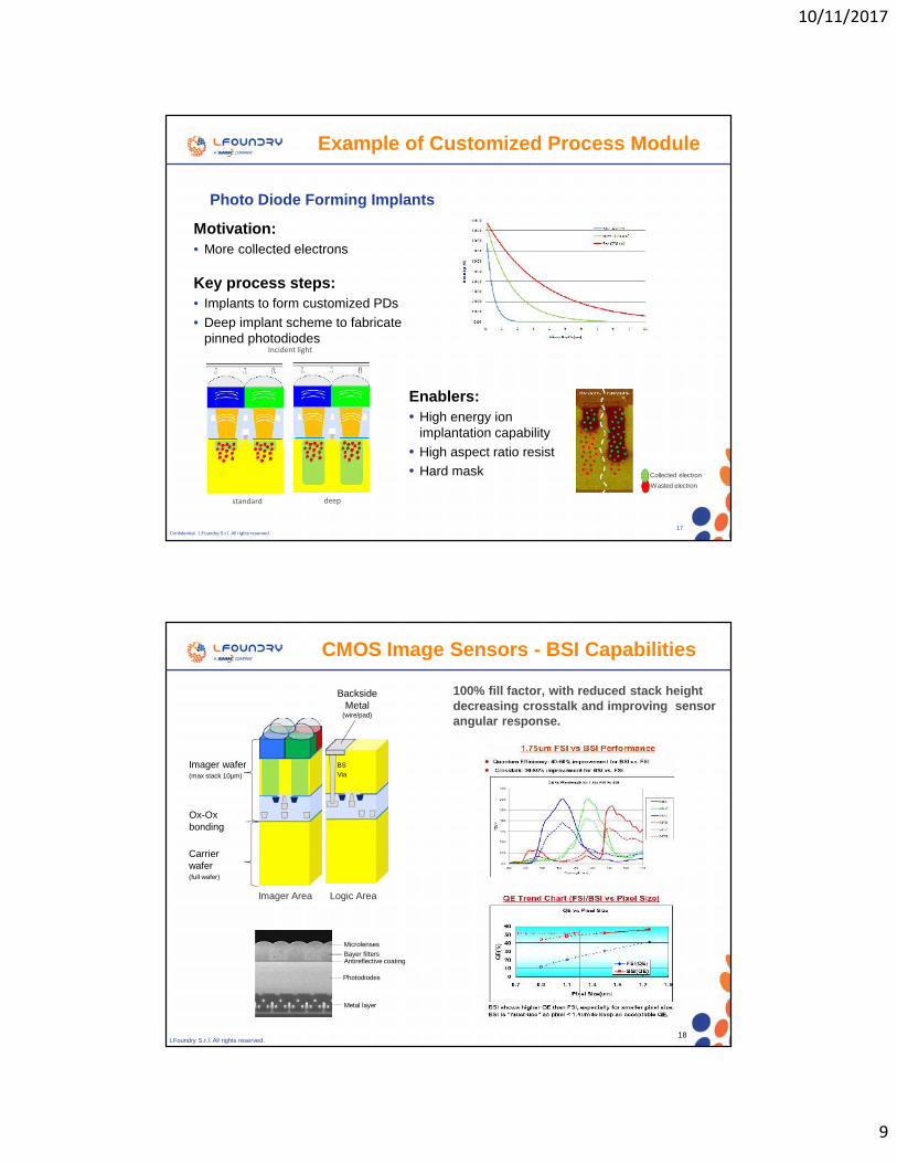
Example of Customized Process Module
Photo Diode Forming Implants
Motivation:• More collected electrons
Key process steps:• Implants to form customized PDs• Deep implant scheme to fabricate
pinned photodiodesIncident light
standard deep
Enablers:• High energy ion
implantation capability• High aspect ratio resist• Hard mask Collected electron
Wasted electron
LFoundry S.r.l. All rights reserved.18
CMOS Image Sensors - BSI Capabilities
Imager wafer(max stack 10µm)
Ox-Oxbonding
Carrierwafer(full wafer)
Imager Area Logic Area
MicrolensesBayer filters
Photodiodes
Metal layer
Antireflective coating
BSVia
BacksideMetal
(wire/pad)
100% fill factor, with reduced stack heightdecreasing crosstalk and improving sensorangular response.
10/11/2017
10
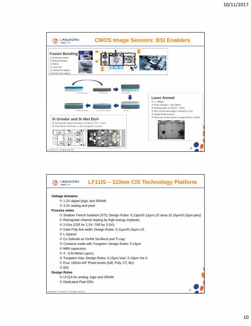
LFoundry S.r.l. All rights reserved.19
CMOS Image Sensors: BSI Enablers
DEVICE WAFER (CIS) CARRIER WAFER WAFER BONDING
BACKSIDE PROCESSING DEVICE WAFER THINNING PAIR FLIP
Laser Anneal l = 308nm; Pulse duration = 160-180ns; Melting depth at 2J/cm2 = 70nm 95% of thermal budget is limited to 3 μm Single Wafer process Max size of laser beam on stage 20mm x 20mmSi Grinder and Si Wet Etch
Post grinder Silicon thickness: 20-30um (TTV < 3 um) Final Silicon Thickness: 2-4um (3 sigma < 0.2um)
Fusion Bonding1) Cleaning module2) Plasma Module3) Robot4) Load Port5) Optical Pre-aligner6) Smart View aligner
Confidential - LFoundry S.r.l. All rights reserved.20
LF11IS – 110nm CIS Technology Platform
Voltage domains 1.2V digital (logic and SRAM) 3.3V analog and pixel
Process notes Shallow Trench Isolation (STI); Design Rules: 0.13µm/0.13µm L/S array (0.15µm/0.15µm pery) Retrograde channel doping by high-energy implants; 2-Gox (22Å for 1.2V; 70Å for 3.3V); Gate Poly line width: Design Rules: 0.11µm/0.15µm L/S L-Spacer Co Salicide w/ Ox/Nit Sa-Block and Ti cap; Contacts made with Tungsten; Design Rules: 0.14µm MIM capacitors; 4 - 6 Al Metal Layers; Tungsten Vias; Design Rules: 0.15µm Via1; 0.19µm Via X Four 193nm ArF Photo levels (Diff, Poly, CT, M1) BSI
Design Rules LF11A for analog, logic and SRAM Dedicated Pixel DRs
10/11/2017
11
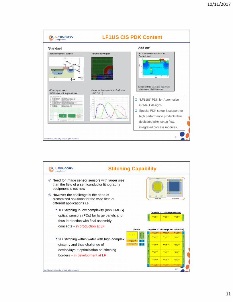
Confidential - LFoundry S.r.l. All rights reserved.21
LF11IS CIS PDK Content
“LF11IS” PDK for Automotive
Grade 1 designs
Special PDK setup & support for
high performance products thru
dedicated pixel setup flow,
integrated process modules, …
Confidential - LFoundry S.r.l. All rights reserved.22
Stitching Capability
Need for image sensor sensors with larger sizethan the field of a semiconductor lithographyequipment is not new
However the challenge is the need ofcustomized solutions for the wide field ofdifferent applications i.e.
• 1D Stitching in low complexity (non CMOS)optical sensors (PDs) for large panels andthus interaction with final assemblyconcepts – in production at LF
• 2D Stitching within wafer with high complexcircuitry and thus challenge ofdevice/layout optimization on stitchingborders – in development at LF
10/11/2017
12
Confidential - LFoundry S.r.l. All rights reserved.23
Outline
• The Avezzano Fab
• The Technology Opportunities
• The Development Perspective
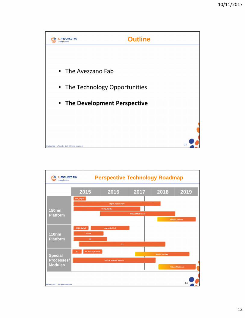
LFoundry S.r.l. All rights reserved.24
2015 2016 2017 2018 2019
150nmPlatform
110nmPlatform
SpecialProcesses/Modules
Perspective Technology Roadmap
24
New BS Devices
AMS, Digital
BCD (LDMOS)
BCD (LDMOS Gen2)
HighT, Automotive
eFlash
HV
AMS, Digital Low-cost eFlash
CIS
BSIWafer Stacking
BS Thinning & Metal
Optical Sensors, Sensors
Silicon Photonics
10/11/2017
13
LFoundry S.r.l. All rights reserved.25
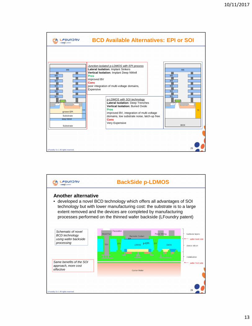
BCD Available Alternatives: EPI or SOI
BOX
TI
M1
M2
M3
M4
M5
M6
grown EPI
Substrate
M1
M2
M3
M4
M5
M6
Substrate
SNK
deep NWell
Junction-isolated p-LDMOS with EPI processLateral Isolation: Implant SinkersVertical Isolation: Implant Deep NWellProsimproved BVConspoor integration of multi-voltage domains,Expensive
p-LDMOS with SOI technologyLateral Isolation: Deep TrenchesVertical Isolation: Buried OxideProsimproved BV, integration of multi-voltagedomains, low substrate noise, latch-up freeConsVery Expensive
LFoundry S.r.l. All rights reserved.26
BackSide p-LDMOS
n+
p-EPI
Schematic of novelBCD technologyusing wafer backsideprocessing
Same benefits of the SOIapproach, more costeffective
Another alternative• developed a novel BCD technology which offers all advantages of SOI
technology but with lower manufacturing cost: the substrate is to a largeextent removed and the devices are completed by manufacturingprocesses performed on the thinned wafer backside (LFoundry patent)
10/11/2017
14
Confidential - LFoundry S.r.l. All rights reserved.27
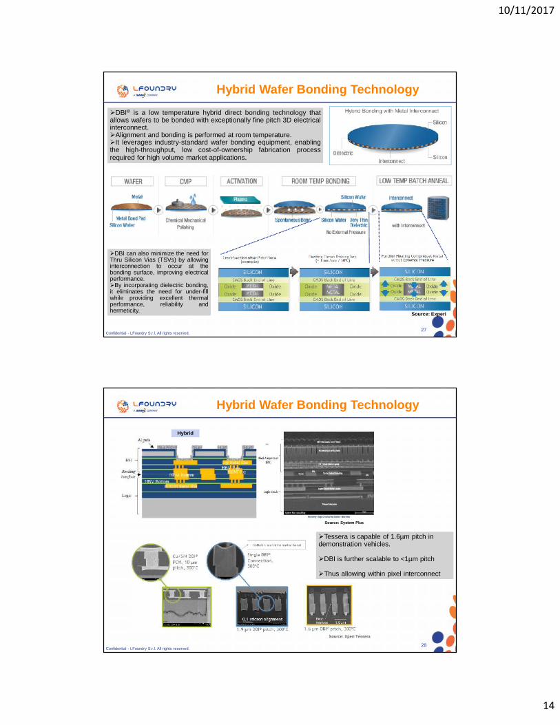
Hybrid Wafer Bonding TechnologyDBI® is a low temperature hybrid direct bonding technology thatallows wafers to be bonded with exceptionally fine pitch 3D electricalinterconnect.Alignment and bonding is performed at room temperature.It leverages industry-standard wafer bonding equipment, enablingthe high-throughput, low cost-of-ownership fabrication processrequired for high volume market applications.
DBI can also minimize the need forThru Silicon Vias (TSVs) by allowinginterconnection to occur at thebonding surface, improving electricalperformance.By incorporating dielectric bonding,it eliminates the need for under-fillwhile providing excellent thermalperformance, reliability andhermeticity. Source: Experi
Confidential - LFoundry S.r.l. All rights reserved.28
Hybrid Wafer Bonding Technology
Hybrid
Source: Xperi Tessera
Tessera is capable of 1.6µm pitch indemonstration vehicles.
DBI is further scalable to <1µm pitch
Thus allowing within pixel interconnect
Source: System Plus
10/11/2017
15
LFoundry S.r.l. All rights reserved.29
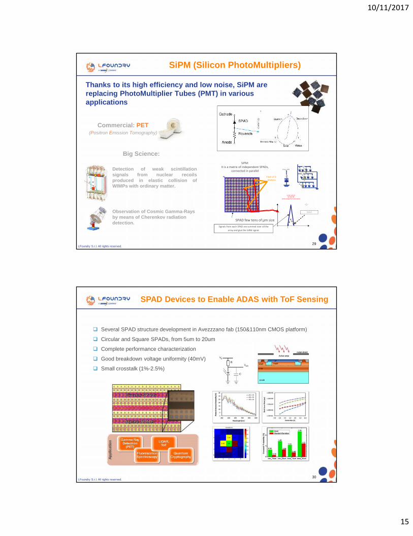
SiPM (Silicon PhotoMultipliers)
Thanks to its high efficiency and low noise, SiPM arereplacing PhotoMultiplier Tubes (PMT) in variousapplications
Commercial: PET(Positron Emission Tomography)
Observation of Cosmic Gamma-Raysby means of Cherenkov radiationdetection.
Big Science:
Detection of weak scintillationsignals from nuclear recoilsproduced in elastic collision ofWIMPs with ordinary matter.
SiPM:It is a matrix of independent SPADs,
connected in parallel
SPAD few tens of µm size
V=VBD+OV
Flash of 3photons
Q=Q1+Q2+Q3Q1=Q2=Q3
(same charge from each event)
signa
l
Photon arrival time
3Xelementary
pulse
Signals from each SPAD are summed over all thearray and give the SiPM signal.
Elementary pulseSingle SPAD fired
LFoundry S.r.l. All rights reserved.30
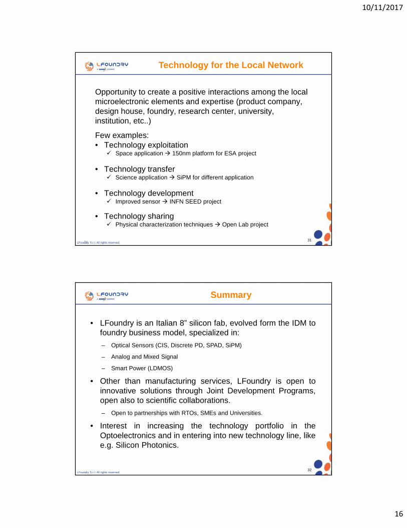
Several SPAD structure development in Avezzzano fab (150&110nm CMOS platform)
Circular and Square SPADs, from 5um to 20um
Complete performance characterization
Good breakdown voltage uniformity (40mV)
Small crosstalk (1%-2.5%)
SPAD Devices to Enable ADAS with ToF Sensing
10/11/2017
16
LFoundry S.r.l. All rights reserved.31
Technology for the Local Network
31
Opportunity to create a positive interactions among the localmicroelectronic elements and expertise (product company,design house, foundry, research center, university,institution, etc..)
Few examples:• Technology exploitation Space application 150nm platform for ESA project
• Technology transfer Science application SiPM for different application
• Technology development Improved sensor INFN SEED project
• Technology sharing Physical characterization techniques Open Lab project
LFoundry S.r.l. All rights reserved.32
Summary
• LFoundry is an Italian 8” silicon fab, evolved form the IDM tofoundry business model, specialized in:– Optical Sensors (CIS, Discrete PD, SPAD, SiPM)
– Analog and Mixed Signal
– Smart Power (LDMOS)
• Other than manufacturing services, LFoundry is open toinnovative solutions through Joint Development Programs,open also to scientific collaborations.– Open to partnerships with RTOs, SMEs and Universities.
• Interest in increasing the technology portfolio in theOptoelectronics and in entering into new technology line, likee.g. Silicon Photonics.
Recommended