Error Canceling Low Voltage SAR-ADC
by
Jianping Wen
A Thesis
submitted to
Oregon State University
in partial fulfillment ofthe requirements for the
degree of
Master of Science
Completed July 26, 2000Commencement June 2001
ACKNOWLEDGMENTS
I would like to express my sincere and deep appreciation to my academic advi-
sors, Dr. Gabor C. Temes and Dr. Un-Ku Moon, for the research project and excellent
academic environment they provided for me. I have been honored and privileged to
have worked under their supervision. Without their warm encouragement and aca-
demic guidance as well as their generous support, it would be impossible for me to
complete the work presented in this thesis.
Special thanks are extended to Dr. Byung-Moo Min for his competent expertise
in circuit design that greatly helped me in the transistor level implementations of the
designed A/D converter. The author also wants to thank Dr. Kyoung-Rok Cho for
the valuable discussion on digital circuit design.
I would like to express my appreciation to Dr. John T. Stonick for many enlight-
ening discussions and comments on my research during our regular weekly research
group meetings.
I also would like to thank Prof. Robert J. Schultz for taking time out of his busy
schedule to serve as the Graduate Council Representative of my committee.
Many thanks, also, to Mr. Jose Silva for his kind help with his wonderful skills in
various CAD tools. Without his help, I could not be able to complete my thesis now
but I would still be exploring the details of those necessary CAD tools for my design.
I wish to thank my colleagues in our research group, Mr. Tetsuya Kajita, Mr.
Mustafa Keskin, Dr. Peter Kiss and Mr. Dong-Yang Chang, for discussions on vari-
ous technical issues on this research project.

I wish to express my thanks to National Semiconductor Corporation for their
financial support to this project and their facilities for fabricating the prototype chip
of this thesis.
Finally, I would like to dedicate this thesis to my wife, Lichun Jia, and my daugh-
ter, Xueyin Wen. I would not be able to finish this thesis without the support of my
loving family.
TABLE OF CONTENTSPage
Chapter 1: Introduction 1
1.1 Motivation . . . . . . . . . . . . . . . . . . . . . . . . . . . . . . . 1
1.2 Thesis Structure . . . . . . . . . . . . . . . . . . . . . . . . . . . . 3
Chapter 2: Mismatch Error Cancellation Algorithm 5
2.1 Conceptual Operation of a Successive Approximation ADC . . . . . 5
2.2 Circuit Non-idealities . . . . . . . . . . . . . . . . . . . . . . . . . 6
2.3 A Novel Capacitor Mismatch Error Cancellation Technique for SwitchedCapacitor SAR – ADC . . . . . . . . . . . . . . . . . . . . . . . . 7
2.4 Improvement of Mismatch Error Cancellation Algorithm . . . . . . 16
Chapter 3: Predictive Correlated Triple Sampling (CTS) 22
3.1 Introduction . . . . . . . . . . . . . . . . . . . . . . . . . . . . . . 22
3.2 Theoretical Analysis of The Switched Capacitor SAR – ADC . . . . 243.2.1 Initial Charges Introduced by Sampling . . . . . . . . . . . 243.2.2 Charge Domain Analysis of Normal Converting Cycles . . . 273.2.3 Calculation of Harmonic Distortion after CDS Compensation 313.2.4 Discussion and Conclusion . . . . . . . . . . . . . . . . . . 32
3.3 Improvement of Predictive CDS in SC SAR – ADC . . . . . . . . . 33
3.4 Verification of Predictive CTS by SWITCAP Simulations of SAR –ADC . . . . . . . . . . . . . . . . . . . . . . . . . . . . . . . . . . 36
Chapter 4: Design of A 1.8V Switched Capacitor SAR – ADC 40
4.1 Introduction . . . . . . . . . . . . . . . . . . . . . . . . . . . . . . 40
4.2 Design Specifications . . . . . . . . . . . . . . . . . . . . . . . . . 40
4.3 Analog Component Design . . . . . . . . . . . . . . . . . . . . . . 42
4.4 Digital Component Design . . . . . . . . . . . . . . . . . . . . . . 50

TABLE OF CONTENTS (Continued)Page
4.4.1 Clock Generator . . . . . . . . . . . . . . . . . . . . . . . . 524.4.2 Finite State Machine . . . . . . . . . . . . . . . . . . . . . 56
4.5 Full Chip Simulation . . . . . . . . . . . . . . . . . . . . . . . . . 57
Chapter 5: Summary and Future Work 61
5.1 Summary . . . . . . . . . . . . . . . . . . . . . . . . . . . . . . . 61
5.2 Plan of Future Work . . . . . . . . . . . . . . . . . . . . . . . . . . 62
Bibliography 63
LIST OF FIGURESFigure Page
2.1 General successive approximation ADC . . . . . . . . . . . . . . . 6
2.2 Circuit of 16 - bit switched-capacitor SAR - A/D converter . . . . . 9
2.3 Circuits of switch setting 1 through switch setting 4 . . . . . . . . . 10
2.4 Circuits of switch setting 5 through switch setting 8 . . . . . . . . . 11
2.5 Circuits of switch setting 9 through switch setting 12 . . . . . . . . 12
2.6 Circuits of switch setting 13 and switch setting 14 . . . . . . . . . . 13
2.7 Mismatch error cancellation for ADD/ADD operation . . . . . . . . 14
3.1 Demonstration of input signal sampling . . . . . . . . . . . . . . . 25
3.2 Demonstration of normal converting cycles . . . . . . . . . . . . . 27
3.3 Harmonic distortion caused by op-amp non-ideality still exists afternormal CDS . . . . . . . . . . . . . . . . . . . . . . . . . . . . . . 31
3.4 predictive CTS operation . . . . . . . . . . . . . . . . . . . . . . . 35
3.5 Output spectrum of a SAR–ADC with predictive CDS, op-amp , no mismatch and parasitic . . . . . . . . . . . 36
3.6 Output spectrum of a SAR–ADC with predictive CTS, op-amp , no mismatch and parasitic . . . . . . . . . . . 37
3.7 Output spectrum of a SAR–ADC with predictive CDS. op-amp , mismatch and parasitic exist . . . . . . . . . . 37
3.8 Output spectrum of a SAR–ADC with predictive CTS. op-amp , mismatch and parasitic exist . . . . . . . . . . 38
4.1 Modification of circuit from normal predictive CDS to double pre-dictive CDS . . . . . . . . . . . . . . . . . . . . . . . . . . . . . . 42
4.2 Implementation of the comparator . . . . . . . . . . . . . . . . . . 43
4.3 Two stage class A/AB operational amplifier . . . . . . . . . . . . . 44
4.4 Bias circuit of the operational amplifier . . . . . . . . . . . . . . . 44
LIST OF FIGURES (Continued)Figure Page
4.5 Switched capacitor common mode feedback circuit . . . . . . . . . 44
4.6 Typical frequency response of the two stage class A/AB operationalamplifier . . . . . . . . . . . . . . . . . . . . . . . . . . . . . . . . 46
4.7 Pre-amplifier of comparator . . . . . . . . . . . . . . . . . . . . . . 47
4.8 Bias circuit of the pre-amplifier of comparator . . . . . . . . . . . . 47
4.9 Comparator latch . . . . . . . . . . . . . . . . . . . . . . . . . . . 48
4.10 NMOS switch-on resistance varies with switch size . . . . . . . . . 49
4.11 CMOS switch-on resistance with different switch sizes vary withsettling voltage . . . . . . . . . . . . . . . . . . . . . . . . . . . . 49
4.12 CMOS switch-on transconductances and . . . . . . . . . . 51
4.13 CMOS switch-on transconductance . . . . 51
4.14 Top level of digital block relative to analog block of the SC SAR–ADC 52
4.15 Timing diagram of the clock generator . . . . . . . . . . . . . . . . 53
4.16 Circuit implementation of clock generator . . . . . . . . . . . . . . 55
4.17 State transition diagram of SAR – ADC . . . . . . . . . . . . . . . 56
4.18 Circuit implementation of state machine . . . . . . . . . . . . . . . 58
4.19 Output spectrum of the switched capacitor SAR – ADC by full chipsimulation . . . . . . . . . . . . . . . . . . . . . . . . . . . . . . . 59
4.20 Layout of the switched-capacitor successive approximation ADC . . 60
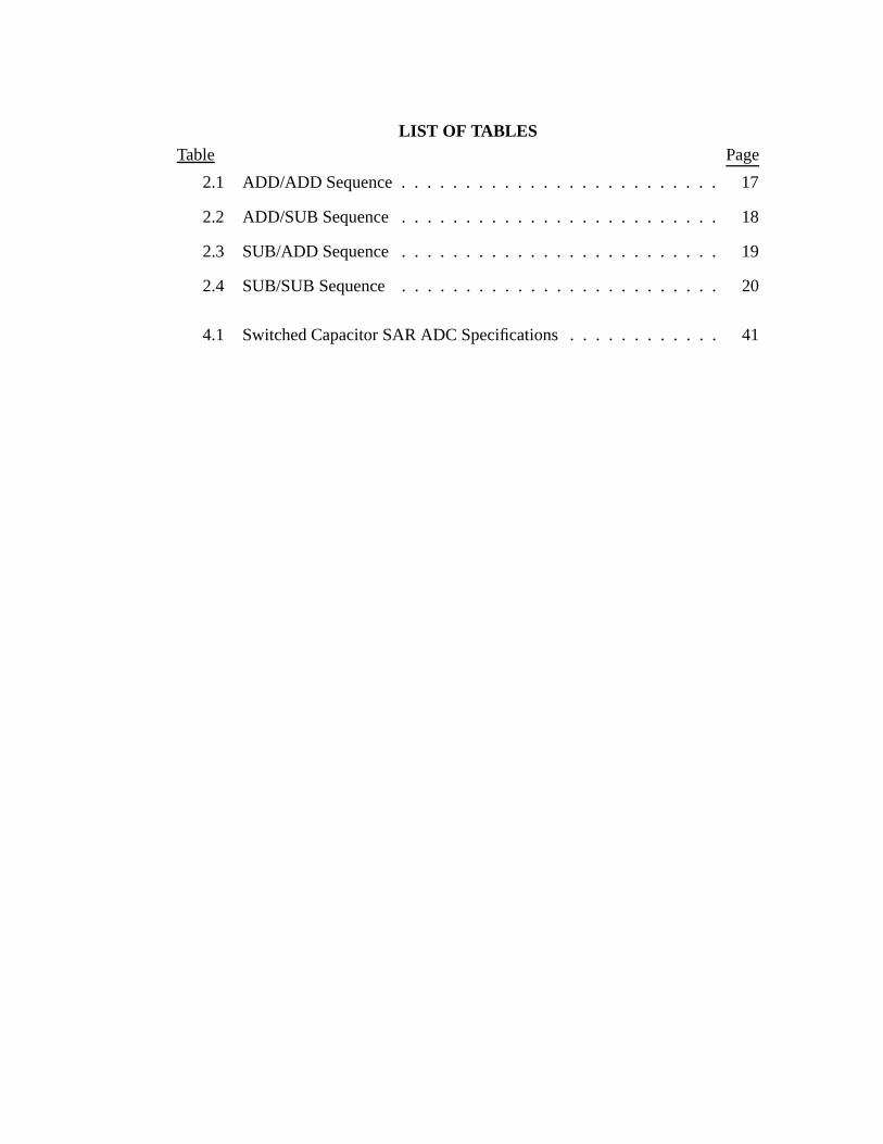
LIST OF TABLESTable Page
2.1 ADD/ADD Sequence . . . . . . . . . . . . . . . . . . . . . . . . . 17
2.2 ADD/SUB Sequence . . . . . . . . . . . . . . . . . . . . . . . . . 18
2.3 SUB/ADD Sequence . . . . . . . . . . . . . . . . . . . . . . . . . 19
2.4 SUB/SUB Sequence . . . . . . . . . . . . . . . . . . . . . . . . . 20
4.1 Switched Capacitor SAR ADC Specifications . . . . . . . . . . . . 41
ERROR CANCELING LOW VOLTAGE SAR-ADC
Chapter 1
Introduction
1.1 Motivation
Signal processing is one of the major incentives to the fast development of electronic
circuits. With the tremendous advancement of modern VLSI technology, people are
able to build more and more complex digital circuits on a single chip to realize signal
processing that is conventionally achieved by analog circuits, because digital circuit
has advantages over its analog counterpart in several aspects such as much lower
noise sensitivity, excellent signal regenerating capability. and it is easier to realize
design and test automation as well. However, the object of signal processing - phys-
ical signals of the real world are always in analog form. Therefore, to facilitate the
extensive DSP functions in the digital domain, interfaces between analog and digi-
tal blocks are omnipresent in all modern mixed signal processing integrated circuits.
Analog to digital data converters are among the major components in the interfaces.
There are three conceptually distinct operations that are performed sequentially
by an A/D converter [17]: (1) It samples a continuous-valued, continuous-time ana-
log signal; (2) it quantizes the sampled signal to a finite number of levels; (3) it assign
a digital code to the related quantized level. With this sequence of operations, any
physical signal, no matter if it is mechanical, thermal, optical, acoustical, or magnet-
ical, once it has been transformed into electrical signal by a proper sensor, it can be
2
converted into digital signal by an A/D converter and processed conveniently with
powerful digital signal processing components, out of which various useful informa-
tion can be extracted.
There are many approaches to realizing the analog-to-digital conversion. Some of
these techniques, such as flash and pipeline [10] A/D converters trade off accuracy for
speed. On the other end of the scale the highest accuracy is realized by oversampling
A/D converters [13, 15], which have high tolerance to technological imperfections
and component parameter variations but low conversion speed and high power con-
sumption. The compromise between conversion speed and accuracy is achieved by
Nyquist rate A/D converters such as algorithmic [9, 11] and successive approximate
A/D converters, which have moderate speed and moderate precision.
Switched capacitor circuits have become popular because of their good linear-
ity and dynamic range. Naturally, switched capacitor techniques are also applied
to Nyquist rate A/D converters. However, if the conversions are realized by simple
charge transfer between ratio-matched capacitors, as it did in the work of McCha-
rles, et al. [11] as an early algorithmic A/D converter, the conversion accuracy will
be fundamentally limited by the ratio accuracy. To overcome this problem, several
circuit configurations have been proposed which perform the cyclic conversion in a
capacitor ratio independent manner [8, 9, 20, 23]. In those approaches the conver-
sion speed was sacrificed for ratio-independent property substantially. For instance,
6 clock cycles were needed for each bit’s conversion in the design of Li, et al. [9]
compared to 2 clocks in [11]. The approach proposed by Onodera, et al. [14] was
able to decrease the number of clocks down to 3 for each bit. A further improve-
ment for conversion speed without losing the ratio-independent feature was realized
by Zheng, et al. [26], where a fully differential circuit structure was used and only 2
clocks were needed for each bit’s conversion, which has the same conversion speed

3
as that of the ratio-dependent structure proposed by McCharles, et al. [11].
Similar to switched-capacitor algorithmic ADC, another type of Nyquist rate
ADC – switched- capacitor successive approximation ADC also suffers from capac-
itor mismatch errors. Apart from developing a ratio-independent circuit structure,
mismatch-shaping techniques ([1, 3, 19]) can be used to decrease the error. The ap-
proach proposed by Rombouts, et al. [18] realized the first order error cancellation,
where a nearly distortion-free converter is obtained by employing additional signal
processing with the cost of two fold increase of conversion time. To further improve
the switched capacitor successive approximation ADC, a novel mismatch error can-
celing algorithm was proposed by Zheng, et al. [27], where only 50% of conversion
time is needed to eliminate the first order mismatch error. As the continuation of
this research, this thesis aims to improve the proposed algorithm and realize the cir-
cuit on a chip, which will be the test vehicle for the proposed circuitry for further
improvement.
1.2 Thesis Structure
Chapter 2 describes the principle of successive approximate A/D converters, and gen-
eral considerations of circuit non-ideality in realizing a switched capacitor successive
A/D converter. Based on the detailed charge domain analysis of the ADC operations,
an improvement of the algorithm proposed by Zheng, et al. [27] is provided by trac-
ing the error charge free capacitor. To summarize the complete algorithm, 4 tables
4
representing the detailed operational sequences of the ADC to be designed are pro-
vided at the end of this chapter.
Chapter 3 studies the characteristics of the predictive correlated double sampling
technique in switched capacitor successive approximation ADC. A detailed theoret-
ical analyze of the operations of the proposed SC SAR–ADC is given. MATLAB
simulations based on the theoretical results show that the conventional predictive
CDS is not adequate to achieve high resolution SC SAR–ADC. The subtle difference
in signal processing manners between predictive CDS in SC SAR-ADC and other ap-
plications is discussed. Further more, the predictive correlated triple sampling (CTS)
technique is proposed to improve the inadequacy of predictive CDS in SAR–ADC,
and this improvement is verified by SWITCAP simulations.
Chapter 4 gives the detailed design of the proposed SC SAR–ADC with National
Semiconductor low voltage technology. Transistor level full chip simulation is given
at the end of this chapter.
Chapter 5 summarizes the work of this thesis and the plan of future work.
5
Chapter 2
Mismatch Error Cancellation Algorithm
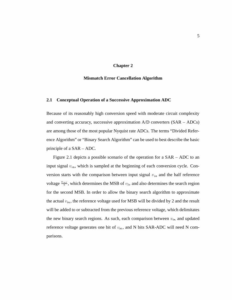
2.1 Conceptual Operation of a Successive Approximation ADC
Because of its reasonably high conversion speed with moderate circuit complexity
and converting accuracy, successive approximation A/D converters (SAR – ADCs)
are among those of the most popular Nyquist rate ADCs. The terms “Divided Refer-
ence Algorithm” or “Binary Search Algorithm” can be used to best describe the basic
principle of a SAR – ADC.
Figure 2.1 depicts a possible scenario of the operation for a SAR – ADC to an
input signal , which is sampled at the beginning of each conversion cycle. Con-
version starts with the comparison between input signal and the half reference
voltage
, which determines the MSB of and also determines the search region
for the second MSB. In order to allow the binary search algorithm to approximate
the actual , the reference voltage used for MSB will be divided by 2 and the result
will be added to or subtracted from the previous reference voltage, which delimitates
the new binary search regions. As such, each comparison between and updated
reference voltage generates one bit of , and N bits SAR-ADC will need N com-
parisons.
6
SARS/H
DAC
Analog Input
Digital Output
V(k)
k2 4 5 6 7 8 9 10 11 1210 3
FIGURE 2.1: General successive approximation ADC
2.2 Circuit Non-idealities
Obviously, the above description is based on the ideal operation of a general SAR
ADC. In real circuits, the “divided by two” operation to the reference voltage can
be realized in various ways. In case of a switched capacitor circuit, it is normally
implemented by sharing reference charge with two matched capacitors, as described
in the paper by Zheng et al. [27]. Therefore any mismatch error between the two
capacitors used to share charge will have a direct impact on the linearity of the overall
converter.
Besides the capacitor mismatch error, there are other circuit non-idealities. In
the low voltage design context, it is difficult to obtain high op-amp gain, thus circuit
imperfection caused by op-amp finite gain is inevitable. Other non-avoidable circuit
7
non idealities include op-amp offset voltage, parasitic capacitances, charge injection
and clock feedthrough, etc. The following is a brief description of a novel technique
proposed by Zheng [25] to cope with above circuit imperfection.
2.3 A Novel Capacitor Mismatch Error Cancellation Technique for SwitchedCapacitor SAR – ADC
A novel capacitor mismatch error cancellation technique for switched capacitor SAR
– ADC has been proposed by Zheng [25]. With this technique, the first order ca-
pacitor mismatch error is virtually eliminated at the cost of increasing by 50% the
data conversion time. This is less than that required in a capacitance ratio inde-
pendent cyclic A/D converter, where typically 100% additional conversion time is
needed compared to the ideal operation. With this technique, not only the capaci-
tance mismatch error has been cancelled, op-amp finite gain and offset voltage are
also compensated by the application of the correlated double sampling (CDS) tech-
nique. Through the proper path arrangement of charge transfer in a fully differential
structure, the influence of top plate parasitic capacitances are also suppressed.
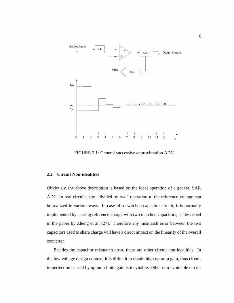
Since there are 16 capacitors in the ADC core, in order to describe the operation
more clearly, it is convenient to have a method for the systematic identification of
each capacitor. The following convention will be used for the identifying subscripts
of the capacitors:
First subscript:
i or int — denotes an integrating capacitor;
r or ref — denotes a capacitor which stores a reference charge;
s or sig — denotes a signal capacitor, which shares charge with reference ca-

8
pacitor;
e or err — denotes an error charge capacitor for CDS compensation.
Second subscript:
1 — denotes capacitors connected to the inverting input side of the fully differ-
ential op-amp;
2 — denotes capacitors connected to the non-inverting input side of the fully
differential op-amp.
Third subscript:
D or DAC — denotes CDS error charge capacitors of the op-amp;
C or Comp — denotes CDS error charge capacitors of the comparator;
p(predicting) — denotes capacitors used in predicting phase (of CDS opera-
tion);
c(converting) — denotes capacitors used in converting phase (of CDS opera-
tion).
Then, the 16 capacitors in the circuit are
9
S04
S11
S12
S17
S13
S19
S21
S23
S35
S39 S4
1
S43
S45
S47
S46
S44
S37
S20
S16
S22
S24
S15
S49
S51
S52
S54
S53
S59
S61
S65
S66
S62
S67
S68
S72
S64
S42
S18
S36
S38
S40
S50
S60
S48
S29
S05
S09
S07
S03
S55
S57
S63
S69
S70
S71
S08
S32
S31
S10
S30
S58
S56
N01
N03
N09
N05
N07
N08
N04
N02
N14
N16
N20
N19
N13
N15
N21
N23
N22
N24
N29
N31
N25
N27
N30
N32
N26
N28
N33
N34
N36
N38
N35
N37
N39
N40
S02
S01
N10
S14
S06
N06
S28
S27
N17
N18
S26
S25
N11
N12
+
FIG
UR
E2.
2:C
ircu
itof
16-
bits
witc
hed-
capa
cito
rSA
R-
A/D
conv
erte
r
10
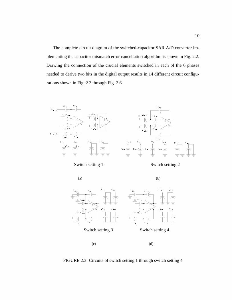
The complete circuit diagram of the switched-capacitor SAR A/D converter im-
plementing the capacitor mismatch error cancellation algorithm is shown in Fig. 2.2.
Drawing the connection of the crucial elements switched in each of the 6 phases
needed to derive two bits in the digital output results in 14 different circuit configu-
rations shown in Fig. 2.3 through Fig. 2.6.
Switch setting 1
(a)
Switch setting 2
(b)
Switch setting 3
(c)
Switch setting 4
(d)
FIGURE 2.3: Circuits of switch setting 1 through switch setting 4
11
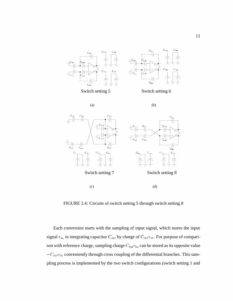
Switch setting 5
(a)
Switch setting 6
(b)
Switch setting 7
(c)
Switch setting 8
(d)
FIGURE 2.4: Circuits of switch setting 5 through switch setting 8
Each conversion starts with the sampling of input signal, which stores the input
signal in integrating capacitor by charge of . For purpose of compari-
son with reference charge, sampling charge can be stored as its opposite value
conveniently through cross coupling of the differential branches. This sam-
pling process is implemented by the two switch configurations (switch setting 1 and
12
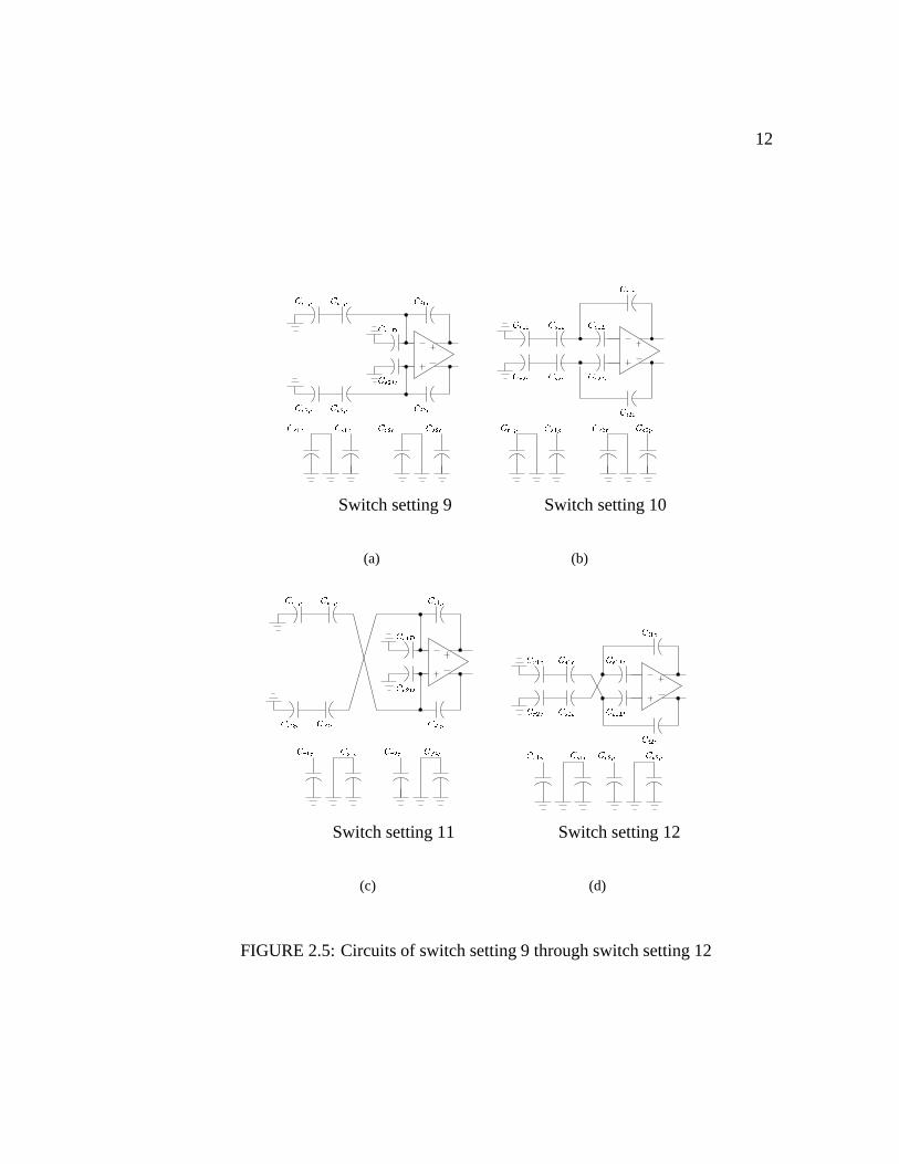
Switch setting 9
(a)
Switch setting 10
(b)
Switch setting 11
(c)
Switch setting 12
(d)
FIGURE 2.5: Circuits of switch setting 9 through switch setting 12
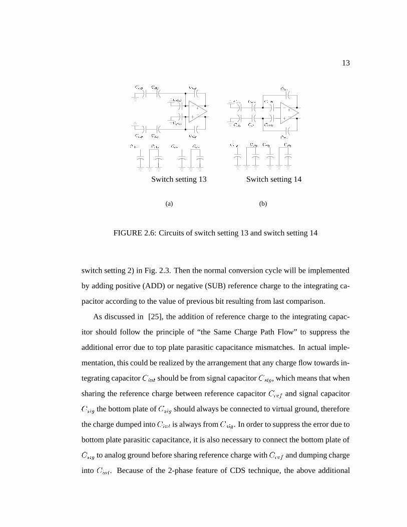
13
Switch setting 13
(a)
Switch setting 14
(b)
FIGURE 2.6: Circuits of switch setting 13 and switch setting 14
switch setting 2) in Fig. 2.3. Then the normal conversion cycle will be implemented
by adding positive (ADD) or negative (SUB) reference charge to the integrating ca-
pacitor according to the value of previous bit resulting from last comparison.
As discussed in [25], the addition of reference charge to the integrating capac-
itor should follow the principle of “the Same Charge Path Flow” to suppress the
additional error due to top plate parasitic capacitance mismatches. In actual imple-
mentation, this could be realized by the arrangement that any charge flow towards in-
tegrating capacitor should be from signal capacitor , which means that when
sharing the reference charge between reference capacitor and signal capacitor
the bottom plate of should always be connected to virtual ground, therefore
the charge dumped into is always from . In order to suppress the error due to
bottom plate parasitic capacitance, it is also necessary to connect the bottom plate of
to analog ground before sharing reference charge with and dumping charge
into . Because of the 2-phase feature of CDS technique, the above additional

14
FIGURE 2.7: Mismatch error cancellation for ADD/ADD operation
15
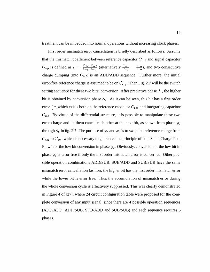
treatment can be imbedded into normal operations without increasing clock phases.
First order mismatch error cancellation is briefly described as follows. Assume
that the mismatch coefficient between reference capacitor and signal capacitor
is defined as
(alternatively
), and two consecutive
charge dumping (into ) is an ADD/ADD sequence. Further more, the initial
error-free reference charge is assumed to be on . Then Fig. 2.7 will be the switch
setting sequence for these two bits’ conversion. After predictive phase , the higher
bit is obtained by conversion phase . As it can be seen, this bit has a first order
error , which exists both on the reference capacitor and integrating capacitor
. By virtue of the differential structure, it is possible to manipulate these two
error charge and let them cancel each other at the next bit, as shown from phase
through in fig. 2.7. The purpose of and is to swap the reference charge from
to , which is necessary to guarantee the principle of “the Same Charge Path
Flow” for the low bit conversion in phase . Obviously, conversion of the low bit in
phase is error free if only the first order mismatch error is concerned. Other pos-
sible operation combinations ADD/SUB, SUB/ADD and SUB/SUB have the same
mismatch error cancellation fashion: the higher bit has the first order mismatch error
while the lower bit is error free. Thus the accumulation of mismatch error during
the whole conversion cycle is effectively suppressed. This was clearly demonstrated
in Figure 4 of [27], where 24 circuit configuration table were proposed for the com-
plete conversion of any input signal, since there are 4 possible operation sequences
(ADD/ADD, ADD/SUB, SUB/ADD and SUB/SUB) and each sequence requires 6
phases.
16
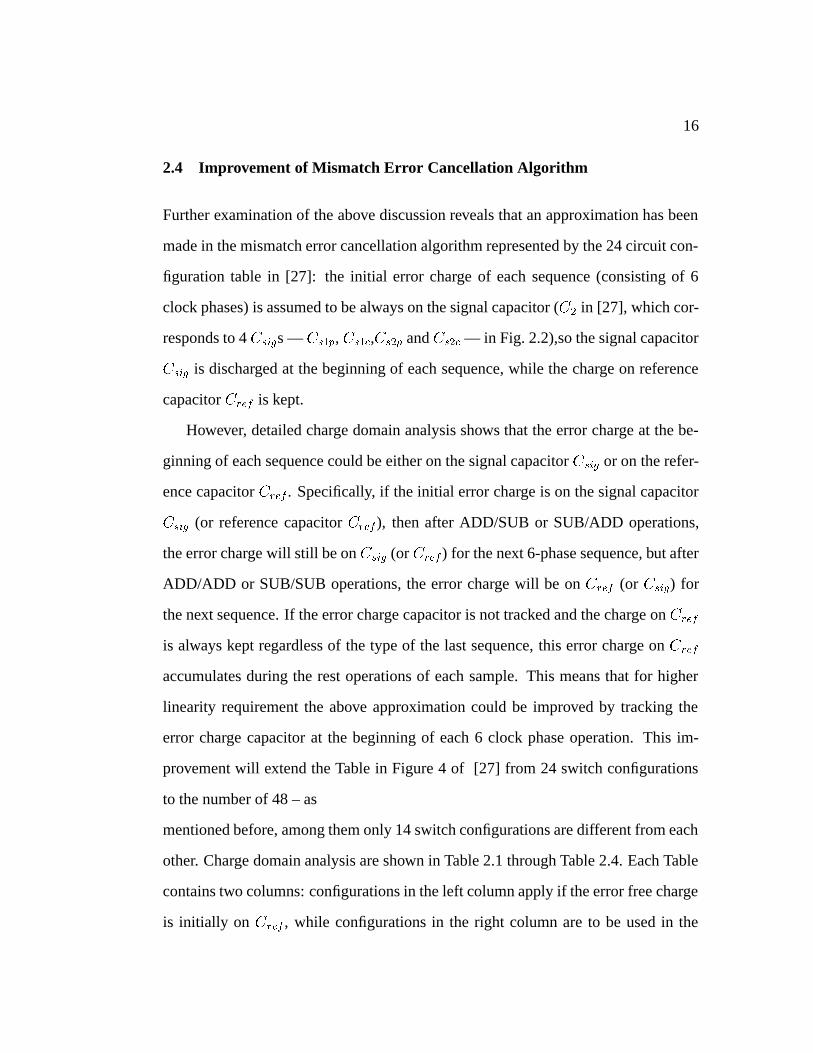
2.4 Improvement of Mismatch Error Cancellation Algorithm
Further examination of the above discussion reveals that an approximation has been
made in the mismatch error cancellation algorithm represented by the 24 circuit con-
figuration table in [27]: the initial error charge of each sequence (consisting of 6
clock phases) is assumed to be always on the signal capacitor ( in [27], which cor-
responds to 4 s — , , and — in Fig. 2.2),so the signal capacitor
is discharged at the beginning of each sequence, while the charge on reference
capacitor is kept.
However, detailed charge domain analysis shows that the error charge at the be-
ginning of each sequence could be either on the signal capacitor or on the refer-
ence capacitor . Specifically, if the initial error charge is on the signal capacitor
(or reference capacitor ), then after ADD/SUB or SUB/ADD operations,
the error charge will still be on (or ) for the next 6-phase sequence, but after
ADD/ADD or SUB/SUB operations, the error charge will be on (or ) for
the next sequence. If the error charge capacitor is not tracked and the charge on
is always kept regardless of the type of the last sequence, this error charge on
accumulates during the rest operations of each sample. This means that for higher
linearity requirement the above approximation could be improved by tracking the
error charge capacitor at the beginning of each 6 clock phase operation. This im-
provement will extend the Table in Figure 4 of [27] from 24 switch configurations
to the number of 48 – as
mentioned before, among them only 14 switch configurations are different from each
other. Charge domain analysis are shown in Table 2.1 through Table 2.4. Each Table
contains two columns: configurations in the left column apply if the error free charge
is initially on , while configurations in the right column are to be used in the
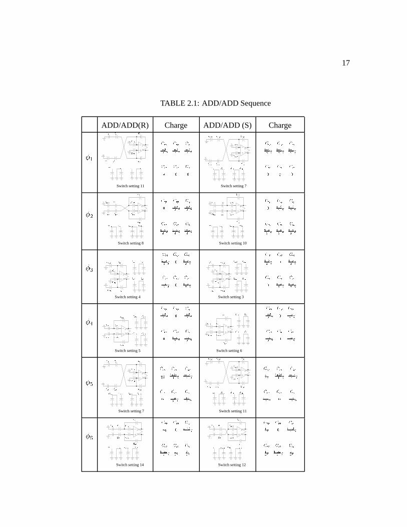
17
TABLE 2.1: ADD/ADD Sequence
ADD/ADD(R) Charge ADD/ADD (S) Charge
Switch setting 11
Switch setting 7
Switch setting 8
Switch setting 10
Switch setting 4
Switch setting 3
Switch setting 5
Switch setting 6
Switch setting 7
Switch setting 11
Switch setting 14
Switch setting 12
18
TABLE 2.2: ADD/SUB Sequence
ADD/SUB(R) Charge ADD/SUB (S) Charge
Switch setting 11
Switch setting 7
Switch setting 8
Switch setting 10
Switch setting 3
Switch setting 4
Switch setting 6
Switch setting 5
Switch setting 13
Switch setting 9
Switch setting 14
Switch setting 12

19
TABLE 2.3: SUB/ADD Sequence
SUB/ADD(R) Charge SUB/ADD (S) Charge
Switch setting 13
Switch setting 9
Switch setting 10
Switch setting 8
Switch setting 3
Switch setting 4
Switch setting 6
Switch setting 5
Switch setting 11
Switch setting 7
Switch setting 12
Switch setting 14

20
TABLE 2.4: SUB/SUB Sequence
SUB/SUB(R) Charge SUB/SUB (S) Charge
Switch setting 13
Switch setting 9
Switch setting 10
Switch setting 8
Switch setting 4
Switch setting 3
Switch setting 5
Switch setting 6
Switch setting 9
Switch setting 13
Switch setting 12
Switch setting 14

21
sequence if the error free charge is initially on . Notice that in these tables two
mismatch coefficients have been used: is for conversion phase related capacitors
and is for prediction phase related capacitors.
22
Chapter 3
Predictive Correlated Triple Sampling (CTS)
3.1 Introduction
As discussed in chapter 2, circuit non-idealities exist in any switched capacitor cir-
cuit, such as op-amp finite gain and offset voltage, parasitic capacitances, signal de-
pendent charge injection, and nonlinear charge/voltage characteristics of the capaci-
tors, etc. These circuit non-idealities cause nonlinear distortions in the performance
of switched capacitor circuits. Since a low voltage switched capacitor SAR - ADC is
to be designed in this thesis and it is difficult to obtain very high op-amp gain in the
normal signal range, finite gain and offset voltage must be of concern.
The correlated double sampling (CDS) technique [2, 4, 5, 7, 12, 21, 22, 24] is
well known and widely used in switched capacitor circuits, such as SC S/H and delay
stages, integrators, equalizers and amplifiers. It is proved that this technique can be
used in switched capacitor circuit to effectively suppress nonlinear distortions thus
the technique has been imbedded into the design of the switched capacitor SAR –
ADC in this thesis. The essence of predictive CDS adopted into the design described
in chapter 2 is that during the predictive phase, voltage deviation of virtual ground
due to finite gain and offset voltage from analog ground is stored in error capacitor
, and in the conversion phase this error charge will be kept and bring the “pivot”
of charge transfer between signal capacitor and integrating capacitor to a
voltage value closer to the analog ground, or the charge transfer “pivot” exhibits less
23
voltage deviation from analog ground than op-amp virtual ground does, which en-
sures more ideal charge transfer between and hence less distortion after the
signal passes the designed SC stage. There is a subtle difference between the appli-
cations of CDS in the above mentioned SC circuits and in successive approximation
ADC. For the normal applications of CDS in SC circuits such as S/H and integra-
tor stages, signal passes the designed SC stage once, higher order errors after CDS
compensation is negligible compared to the magnitude of processed signal itself. But
in case of SAR – ADC, the processed signal is the reference voltage that passes the
designed integrating stage (behaves as an internal DAC) repeatedly, any small error
after normal CDS compensation will be accumulated and amplified (according to
the capacitance ratio) N times (number of bits generated by the ADC). On the other
hand, the processed signal itself (the reference voltage) is halved each time it passes
the integrating stage, therefore the error left over after CDS compensation in SAR –
ADC may not be negligible compared to the processed signal and causes significant
nonlinear distortions.
This chapter starts from the theoretical analysis of the operation of the designed
switched capacitor SAR – ADC described in chapter 2 and shows that the normal pre-
dictive CDS is not good enough for high resolution SAR – ADCs. Then an improve-
ment of the predictive CDS is proposed based on the operation of normal predictive
CDS. SWITCAP simulations of the SAR – ADC given in chapter 2 are performed
to verify this improvement. This new version of the predictive CDS technique – “
24
predictive Correlated Triple Sampling (CTS) technique” – which is proposed and
verified in this chapter, is used in the final design discussed in chapter 4.
3.2 Theoretical Analysis of The Switched Capacitor SAR – ADC
The predictive CDS technique in the switched capacitor SAR – ADC will be explored
in this section under the condition that the only circuit non-idealities are from op-
amp finite gain and offset voltage, while all capacitors have the same value. Data
conversion follows the same switch sequences described in chapter 2, except that
the charge swap procedures ( and ) between high bit and low bit conversion are
omitted. As mentioned in chapter 2, and transfer charge either from signal
capacitor to the reference capacitor or vice versa to guarantee the “same
path charge flow” principle. Obviously this charge transfer is not complete because
of voltage deviation of op-amp virtual ground from analog ground. Since it is difficult
to mathematically track the direction of charge transfer, this analysis simply assumes
that this charge transfer is complete and exactly the same amount of reference charge
will be used in the following low bit conversion. However, even with this somewhat
ideal implementation, observable nonlinear distortion still appears.
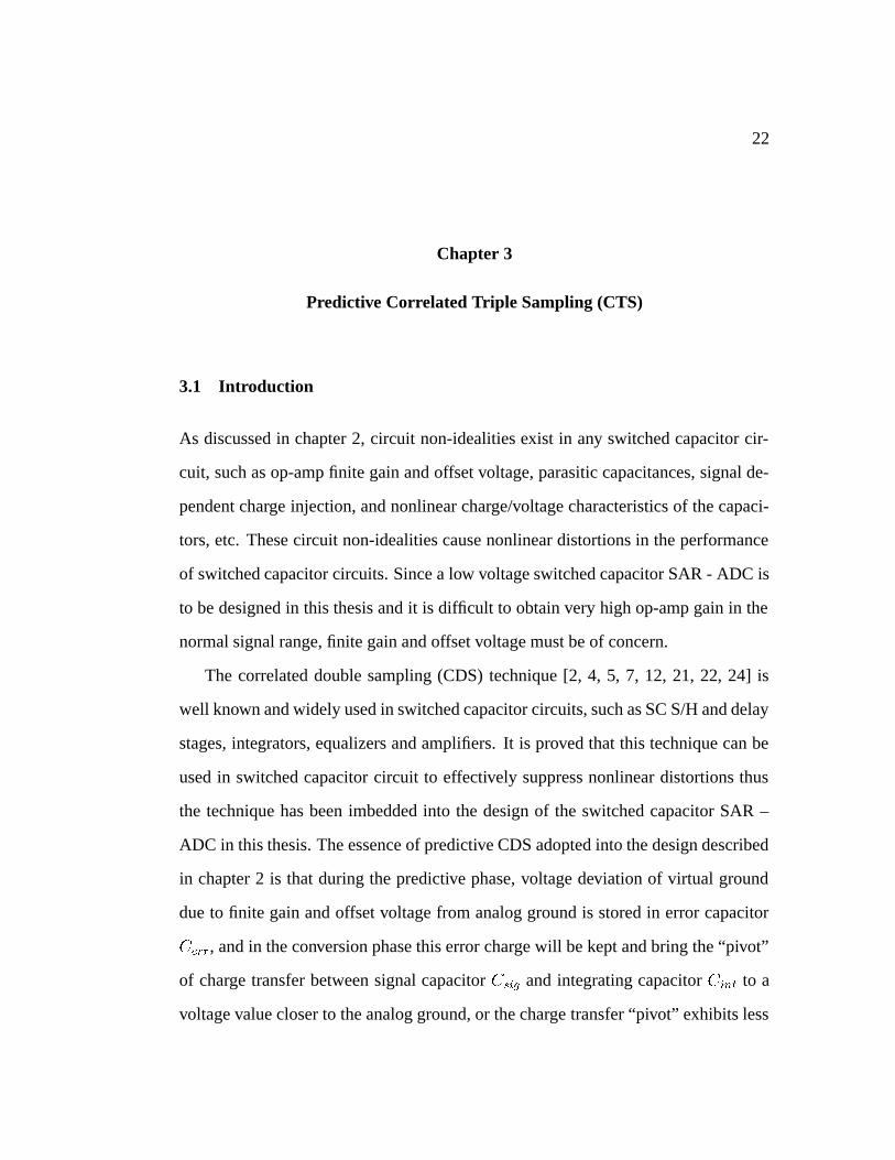
3.2.1 Initial Charges Introduced by Sampling
The sampling of the signal is performed by two switch settings (prediction phase
and actual sampling phase) demonstrated in Fig. 3.1. These two steps bring signal
charge into integrating capacitor and reference charge into reference capacitor .
Notice that the second subscript ‘’ or ‘’ for capacitors is used to denote prediction
phase and conversion phase. Obviously the error capacitor will be charged during
prediction phase because of op-amp finite gain and offset voltage. Equations
25
n
A
(a)
n
A
c
(b)
FIGURE 3.1: Demonstration of input signal sampling
necessary to describe the sampling phase are:
(3.1)
(3.2)
Solving the above two equations and using notation , it is found that
(3.3)
with the assumption ,
(3.4)
and
(3.5)
which gives the error charge on caused by op-amp finite gain and offset voltage,
and charge on integrating capacitor
(3.6)
26
(3.7)
The error charge on will remain unchanged during sampling phase .
Equations necessary to describe the sampling phase are:
(3.8)
(3.9)
Solving the above two equations (with the assumption ), it
is found that
(3.10)
(3.11)
which gives
(3.12)
During sampling phase , reference capacitors and are charged with
reference voltage , which give the initial reference charge
(3.13)
(3.14)
Eq. 3.6, Eq. 3.7, Eq. 3.12, Eq. 3.13 and Eq. 3.14 provide the initial charges in the
circuit for the rest of converting cycles of signal . At the same time, the polarity
of calculated by Eq. 3.10 determines the MSB:
if
otherwise

27
A
n
r
(a)
r
A
n
c
(b)
FIGURE 3.2: Demonstration of normal converting cycles
3.2.2 Charge Domain Analysis of Normal Converting Cycles
With all necessary initial charges in hand, it is possible now to proceed with the
charge domain analysis of the normal converting cycles. Since all converting cycles
repeat the same switch sequence (again for mathematical simplicity two charge swap
phases and of actual implementation in chapter 2 are ignored, as explained
in the last section), it is proper to deal with this problem in an iteration manner.
The following analysis assumes that for the th bit cycle, error charge , reference
charges and , integrating charges and are left over by the bit cycle.
Circuit configurations of both and for normal converting cycles are illustrated
in Fig. 3.2.
It is worth mentioning that Fig. 3.2 is sufficient to represent both cases of direct
coupling and cross coupling in a differential structure described in chapter 2, where
the manner of coupling varies with ADD or SUB operations. Notice that Fig. 3.2
agrees with the direct coupling configuration of [27], which corresponds to a SUB
operation. Mathematical treatment in this analysis for cross coupling is described
28
as following: (1) When the new reference charges and are to be calculated for
cross coupling configuration, it is necessary to flip the signs of the initial error charge
, integrating charges and , while the signs of initial reference charges
and remain unchanged; (2) with the new error charge , integrating charges
and are calculated, and the signs of and should be flipped, while the signs
of , and remain unchanged.
Equations necessary to describe predicting phase are:
(3.15)
(3.16)
(3.17)
Solving the above three equations, using notation and assuming
, it is found that
(3.18)
(3.19)
which gives
(3.20)
(3.21)
(3.22)
29
Note that in the above derivations a sign factor has been introduced
to take care of the cross coupling circuit configuration when an ADD operation is
needed. Here is the value of th bit, which means that if a set
of SUB operation (direct coupling) formula is obtained, while if the above
formula correspond to an ADD operation (cross coupling). The new error charge
on calculated in phase will remain unchanged during converting phase .
Equations necessary to describe the converting phase are:
(3.23)
(3.24)
(3.25)
Solving the above three equations (with the assumption )
and combining solutions Eq. 3.20 through Eq. 3.22 for converting phase , it is
found that
(3.26)
(3.27)
(3.28)

30
Eq. 3.20, Eq. 3.21,Eq. 3.22,Eq. 3.27 and Eq. 3.28 can be used to calculate the
initial charges for the next bit’s converting, while Eq. 3.26 is used to determine the
digital value of present (th) bit:
if
otherwise
The above formula optimistically describes the charge transportation of the ideal
switched capacitor SAR A/D converter described in chapter 2 since the only imper-
fection is caused by opamp non-ideality and the incomplete charge swap phases
and are ignored. It is easy to use above formula of such a converter to analyze
nonlinear distortions caused only by op-amp finite gain and offset voltage after CDS
compensation.
31
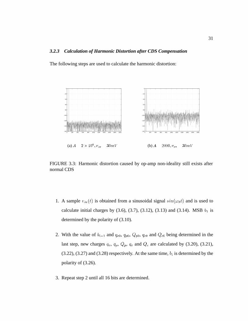
3.2.3 Calculation of Harmonic Distortion after CDS Compensation
The following steps are used to calculate the harmonic distortion:
0 200 400 600 800 1000 1200 1400 1600 1800 2000−160
−140
−120
−100
−80
−60
−40
−20
0
(a)
0 200 400 600 800 1000 1200 1400 1600 1800 2000−160
−140
−120
−100
−80
−60
−40
−20
0
(b)
FIGURE 3.3: Harmonic distortion caused by op-amp non-ideality still exists afternormal CDS
1. A sample is obtained from a sinusoidal signal and is used to
calculate initial charges by (3.6), (3.7), (3.12), (3.13) and (3.14). MSB is
determined by the polarity of (3.10).
2. With the value of and , , , and being determined in the
last step, new charges , , , and are calculated by (3.20), (3.21),
(3.22), (3.27) and (3.28) respectively. At the same time, is determined by the
polarity of (3.26).
3. Repeat step 2 until all 16 bits are determined.

32
4. The decimal representation of this sample is calculated from 16-bit digital out-
put.
5. Go to step 1 for the next sample.
6. Repeat above procedure until 4096 samples are converted which contain 67
bins.
7. FFT calculation is performed for these 4096 samples.
The output spectra of this A/D converter with perfectly matched capacitors are
dipicted in Fig. 3.3.
3.2.4 Discussion and Conclusion
The above theoretical analysis of a switched-capacitor SAR A/D converter with per-
fectly matched capacitors shows that observable harmonic distortion still exists even
when the op-amp finite gain and offset voltage are compensated by the normal CDS
technique. This should be reasonable because even CDS technique decreases virtual
ground voltage dramatically compared to the case without CDS, the voltage of the
virtual ground still exhibits a finite small deviation from the analog ground. Therefore
charge transfers across virtual ground can never be complete, which means that the
division of reference charge will deviate from the ideal factor 1/2 for each bit. This
deviation is negligible for determining the polarity of when integrating charge
is significantly different than zero. However, this deviation, even small for each
bit because of CDS compensation, should accumulate as converting continues. On
the other hand the integrating charge approaches zero as the reference charge is
being halved for each bit. After a certain number of bits’ conversion, the magnitude
33
of will be comparable to the accumulated error and the limit of the converting
resolution is achieved, hence an error code should appear. Because the time when
approaches zero depends on the magnitude of input signal, the above error code is
signal dependent, and appears as harmonic distortion.
3.3 Improvement of Predictive CDS in SC SAR – ADC
The last section reveals that when it is difficult to obtain high gain op-amp, which
is true in case of low voltage design, normal predictive CDS compensation is not
good enough for the high resolution switched capacitor SAR – ADC. However, this
normal predictive CDS technique can be improved with the concept of “Predictive
Correlated Triple Sampling (CTS)” in the context of switched capacitor SAR – ADC,
and this will be explained next.
As mentioned before, the compensation of predictive CDS to op-amp finite gain
and offset voltage happens because the error charge stored on the error capacitor
in the predictive phase brings the “pivot” of the charge transfer in converting phase
closer to the analog ground, which is clearly illustrated in Fig. 3.2. In the predictive
phase , charge transfer “pivot” from to is op-amp virtual ground “”. Due
to op-amp finite gain and offset voltage, voltage of node “” deviates from analog
ground and is stored in as error charge. In converting phase the “pivot” of
charge transfer from to is node “”. As this node in is connected to the
analog ground while the voltage of op-amp virtual ground will not change much
between and and error charge on remains unchanged from to , thus
34
compared to that of node “”, the voltage of node “” is closer to analog ground,
which results in less signal distortion.
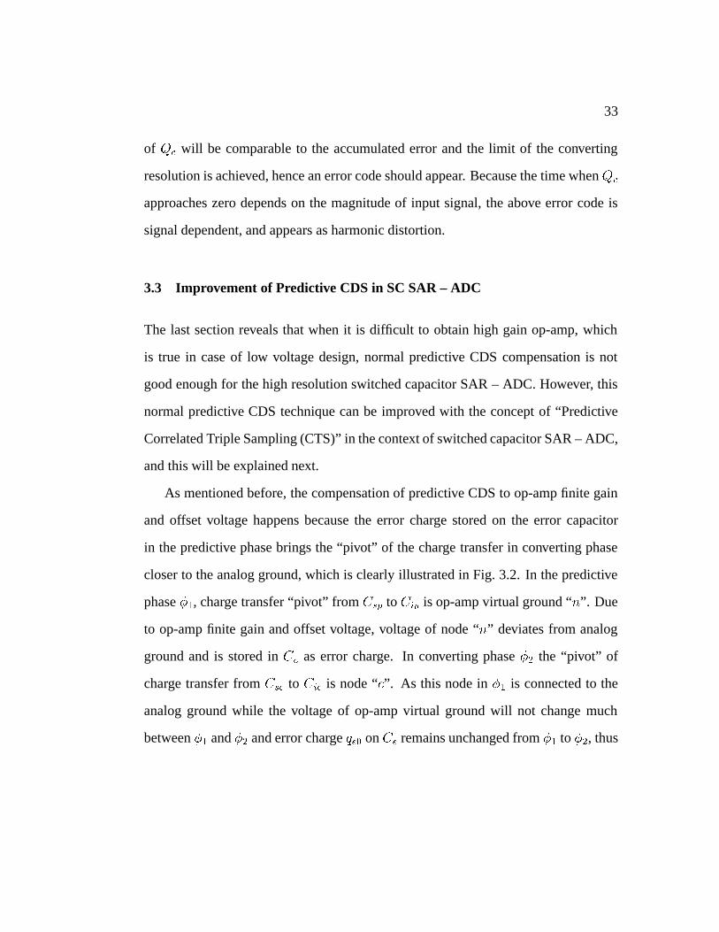
Having understood the above compensation mechanism, it is possible to extend
this mechanism and bring the “pivot” voltage of charge transfer even closer to analog
ground, which is illustrated in Fig. 3.4. Here, three phases have been used to realize
the improved compensation mechanism. In phase , capacitor is charged by er-
ror charge due to op-amp finite gain and offset voltage. This operation is the same as
in the predictive phase of normal predictive CDS except that an additional capacitor
is added and discharged. In phase , node “” is used as the “pivot” of charge
transfer from to , and the small voltage deviation of node “” is stored in .
In phase , node “” is used as the “pivot” of charge transfer from to . With
error charges on both and , voltage of node “” will be closer to the analog
ground than both node “” and node “”. If phase is used in any critical charge
transfer operation while phases and are used in any non-critical ones as predic-
tive operations, then this predictive correlated “triple” sampling (CTS) technique can
increase circuit linearity significantly.
The above predictive CTS inevitably poses a higher burden of clock consumption
to the switched capacitor circuits. Fortunately, in the operation of the successive ap-
proximation ADC it is not necessary to use three phases for all operations. LSB is
the non-critical bit thus and can be used as normal predictive CDS operation
to generate this bit. At the same time the error charge on is refreshed and kept
for and . All bits other than LSB are regarded as critical bits so and are
used as predictive and converting phases respectively to generate those bits. This
arrangement of clock phases will use the same number of clocks as before when nor-
mal predictive CDS technique was used, but higher circuit linearity will be obtained,
as will be shown in the next section by SWITCAP simulations.
35
d c
n
A
d
A
c nd
A
nc
FIGURE 3.4: predictive CTS operation
36
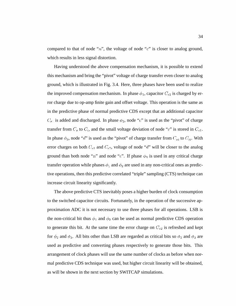
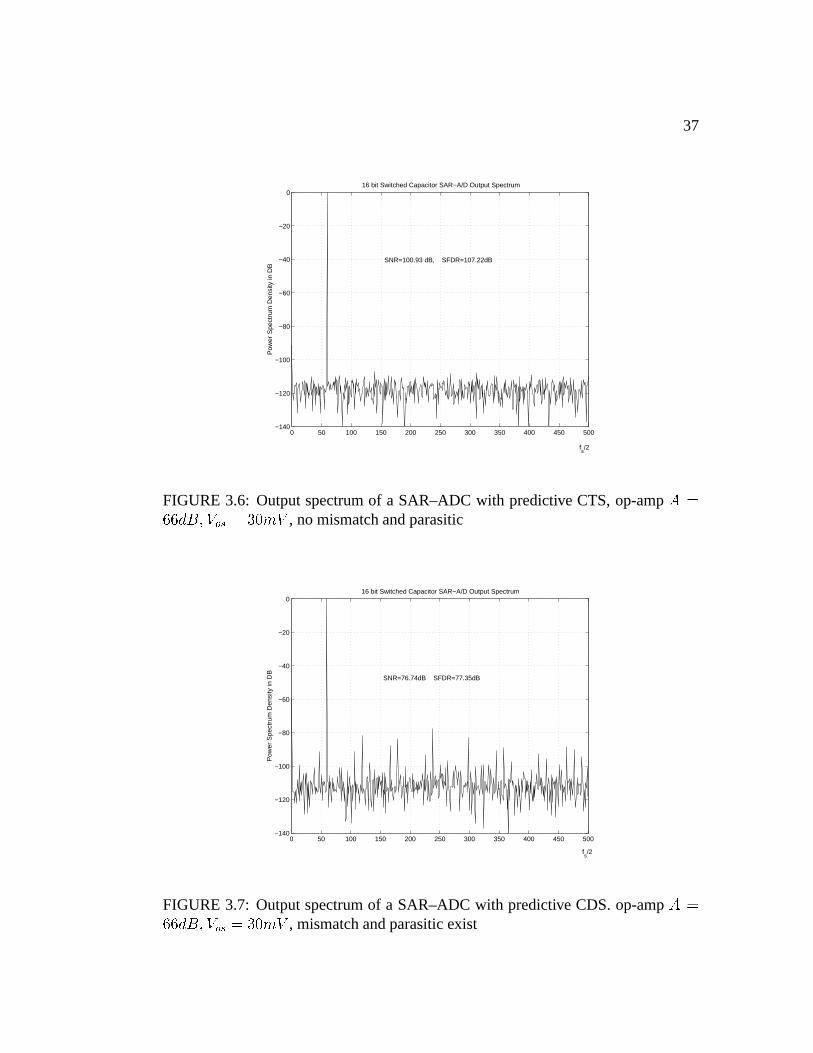
3.4 Verification of Predictive CTS by SWITCAP Simulations of SAR – ADC
SWITCAP simulations have been performed, which compares the improvement of
predictive CTS technique over predictive CDS technique in the operation of SAR –
ADC. Fig. 3.5 shows the output spectrum of the SAR – ADC with predictive CDS
technique, where op-amp gain is 66dB and offset voltage is 30mV. No capacitance
mismatch and parasitic capacitances are included. The same condition is simulated
with predictive CTS technique proposed in this chapter, and the result is shown in
Fig. 3.6.
0 50 100 150 200 250 300 350 400 450 500−140
−120
−100
−80
−60
−40
−20
0
Pow
er S
pect
rum
Den
sity
in D
B
16 bit Switched Capacitor SAR−A/D Output Spectrum
SNR=83.73 dB, SFDR=84.69dB
fs/2
FIGURE 3.5: Output spectrum of a SAR–ADC with predictive CDS, op-amp , no mismatch and parasitic
The improvement of predictive CTS over predictive CDS is obvious: the Signal
to Noise Ratio of 84dB is increased to 101 dB, while the Spur Free Dynamic Range
37
0 50 100 150 200 250 300 350 400 450 500−140
−120
−100
−80
−60
−40
−20
0
Pow
er S
pect
rum
Den
sity
in D
B
16 bit Switched Capacitor SAR−A/D Output Spectrum
SNR=100.93 dB, SFDR=107.22dB
fs/2
FIGURE 3.6: Output spectrum of a SAR–ADC with predictive CTS, op-amp , no mismatch and parasitic
0 50 100 150 200 250 300 350 400 450 500−140
−120
−100
−80
−60
−40
−20
0
Pow
er S
pect
rum
Den
sity
in D
B
16 bit Switched Capacitor SAR−A/D Output Spectrum
SNR=76.74dB SFDR=77.35dB
fs/2
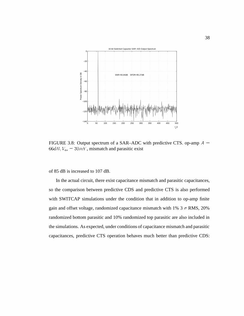
FIGURE 3.7: Output spectrum of a SAR–ADC with predictive CDS. op-amp , mismatch and parasitic exist
38
0 50 100 150 200 250 300 350 400 450 500−140
−120
−100
−80
−60
−40
−20
0
Pow
er S
pect
rum
Den
sity
in D
B
16 bit Switched Capacitor SAR−A/D Output Spectrum
SNR=93.84dB SFDR=95.27dB
fs/2
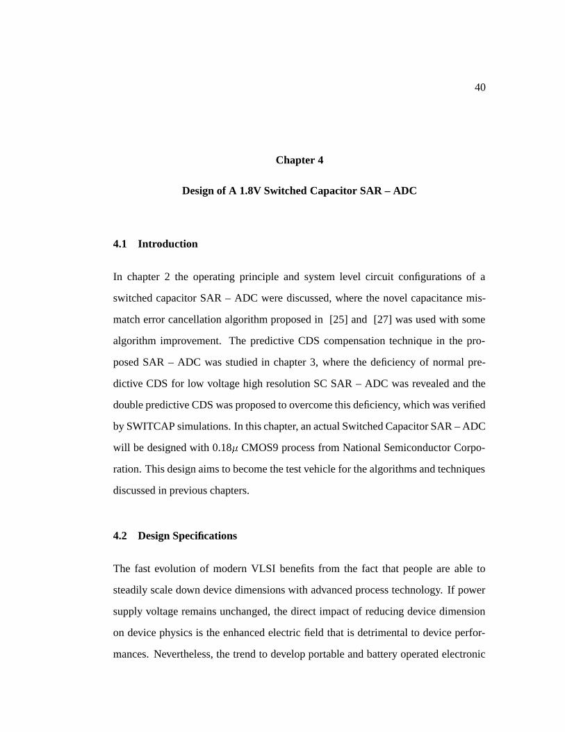
FIGURE 3.8: Output spectrum of a SAR–ADC with predictive CTS. op-amp , mismatch and parasitic exist
of 85 dB is increased to 107 dB.
In the actual circuit, there exist capacitance mismatch and parasitic capacitances,
so the comparison between predictive CDS and predictive CTS is also performed
with SWITCAP simulations under the condition that in addition to op-amp finite
gain and offset voltage, randomized capacitance mismatch with 1% 3 RMS, 20%
randomized bottom parasitic and 10% randomized top parasitic are also included in
the simulations. As expected, under conditions of capacitance mismatch and parasitic
capacitances, predictive CTS operation behaves much better than predictive CDS:

39
the SNR is increased from 76.7dB in Fig. 3.7 to 93.8dB in Fig. 3.8, and SFDR is
increased from 77.4dB in Fig. 3.7 to 95.3dB in Fig. 3.8.
40
Chapter 4
Design of A 1.8V Switched Capacitor SAR – ADC
4.1 Introduction
In chapter 2 the operating principle and system level circuit configurations of a
switched capacitor SAR – ADC were discussed, where the novel capacitance mis-
match error cancellation algorithm proposed in [25] and [27] was used with some
algorithm improvement. The predictive CDS compensation technique in the pro-
posed SAR – ADC was studied in chapter 3, where the deficiency of normal pre-
dictive CDS for low voltage high resolution SC SAR – ADC was revealed and the
double predictive CDS was proposed to overcome this deficiency, which was verified
by SWITCAP simulations. In this chapter, an actual Switched Capacitor SAR – ADC
will be designed with 0.18 CMOS9 process from National Semiconductor Corpo-
ration. This design aims to become the test vehicle for the algorithms and techniques
discussed in previous chapters.
4.2 Design Specifications
The fast evolution of modern VLSI benefits from the fact that people are able to
steadily scale down device dimensions with advanced process technology. If power
supply voltage remains unchanged, the direct impact of reducing device dimension
on device physics is the enhanced electric field that is detrimental to device perfor-
mances. Nevertheless, the trend to develop portable and battery operated electronic

41
instruments requires low power consumption electronics. Therefore low power sup-
ply voltage is a natural choice in modern IC designs to meet above requirements. In
this design 1.8V is chosen as the power supply voltage, which is supported by 0.18
CMOS9 process of National Semiconductor Corporation.
Another target of this design is high resolution, which is chosen as 95dB of dy-
namic range. This aim requires very small kT/C noise from switched capacitor circuit
and determines the lower limit of capacitors used in the circuit. The peak to peak sig-
nal voltage of 1V is used in this design, thus a unit capacitance of 16pF will satisfy
this resolution.
The following table summarizes all parameter specifications of this SAR – ADC.
TABLE 4.1: Switched Capacitor SAR ADC Specifications
Parameter Specification
power supply voltage 1.8V
dynamic range 95 dB
peak to peak input signal swing 1V
input signal bandwidth 0 20kHz
clock frequency 1.4 MHz
technology NSC 0.18 CMOS9 process
The design of this SAR – ADC consists of two blocks: analog components and
42
digital control block for switch clocks. These are described in the following sections.
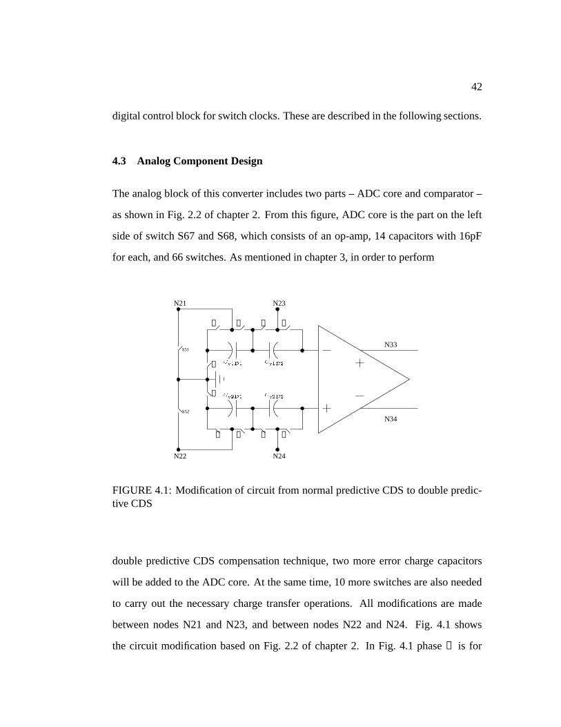
4.3 Analog Component Design
The analog block of this converter includes two parts – ADC core and comparator –
as shown in Fig. 2.2 of chapter 2. From this figure, ADC core is the part on the left
side of switch S67 and S68, which consists of an op-amp, 14 capacitors with 16pF
for each, and 66 switches. As mentioned in chapter 3, in order to perform
➁
➁
N33
N34
➀
➀
➀ ➀
➀➀
➁
S52
S51
N22
N21
N24
N23
➁
FIGURE 4.1: Modification of circuit from normal predictive CDS to double predic-tive CDS
double predictive CDS compensation technique, two more error charge capacitors
will be added to the ADC core. At the same time, 10 more switches are also needed
to carry out the necessary charge transfer operations. All modifications are made
between nodes N21 and N23, and between nodes N22 and N24. Fig. 4.1 shows
the circuit modification based on Fig. 2.2 of chapter 2. In Fig. 4.1 phase ➀ is for
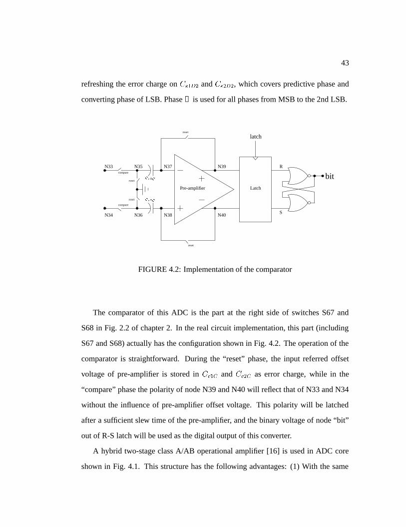
43
refreshing the error charge on and , which covers predictive phase and
converting phase of LSB. Phase ➁ is used for all phases from MSB to the 2nd LSB.
compare
compare
reset
reset
reset
reset
N36 N38
N35 N37 N39
N40N34
N33
Pre-amplifier Latch
latch
R
bit
S
FIGURE 4.2: Implementation of the comparator
The comparator of this ADC is the part at the right side of switches S67 and
S68 in Fig. 2.2 of chapter 2. In the real circuit implementation, this part (including
S67 and S68) actually has the configuration shown in Fig. 4.2. The operation of the
comparator is straightforward. During the “reset” phase, the input referred offset
voltage of pre-amplifier is stored in and as error charge, while in the
“compare” phase the polarity of node N39 and N40 will reflect that of N33 and N34
without the influence of pre-amplifier offset voltage. This polarity will be latched
after a sufficient slew time of the pre-amplifier, and the binary voltage of node “bit”
out of R-S latch will be used as the digital output of this converter.
A hybrid two-stage class A/AB operational amplifier [16] is used in ADC core
shown in Fig. 4.1. This structure has the following advantages: (1) With the same
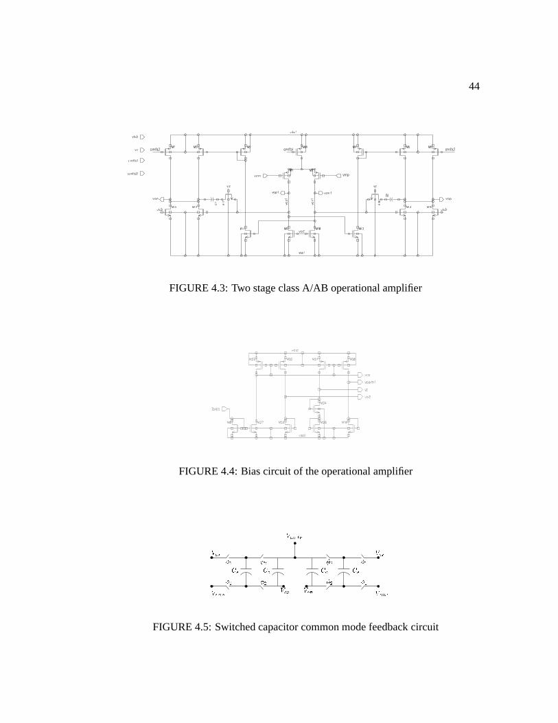
44
FIGURE 4.3: Two stage class A/AB operational amplifier
FIGURE 4.4: Bias circuit of the operational amplifier
FIGURE 4.5: Switched capacitor common mode feedback circuit

45
non-dominant pole frequency, the output branch current is only about half of that of a
two stage class A structure, therefore it consumes less power than a two stage class A
op-amp, this advantage is more obvious in low-speed applications; (2) PSRR is better
than two stage class A; (3)it has a larger signal swing compared to the folded cascode
topology, and this is critical in low voltage design. Fig. 4.3 shows the detailed struc-
ture of this op-amp. Fig. 4.4 is its bias circuit. From Fig. 4.3 it can be seen that bias of
the second stage is determined by the output common mode voltage of the first stage.
A current mirror is used to ensure the “push and pull” operation for the differential
input signal, however, this also cancels the influence of the first stage common mode
voltage on the second stage common mode voltage, which means that two separate
common mode voltage feedback circuits are needed for two stages. The split of tran-
sistors in the output branches is to improve the phase margin of the common mode
feed back loop and adjust the output common mode voltage. The switched capacitor
common mode feedback circuit is used in both stages of this op-amp and is shown
in Fig. 4.5. Capacitances in Fig. 4.5 will affect the phase margin of the op-amp, and
they are determined by simulations of 14 switch configurations described in chapter
2. Even the Bode plot varies somewhat from switch setting to switch setting, the

46
typical one of the op-amp is shown in Fig. 4.6.
101
102
103
104
105
106
107
108
−200
−150
−100
−50
0
50
100
Frequency (Hz)
Pha
se(d
eg),
Gai
n(dB
)
Gain
Phase
FIGURE 4.6: Typical frequency response of the two stage class A/AB operationalamplifier
Fig. 4.7 shows the circuit for the pre-amplifier used in the comparator. This is
a normal folded cascode amplifier, and its bias circuit is shown in Fig. 4.8. The
common mode feedback circuit of this folded cascode pre-amplifier has the same
structure as Fig. 4.5.
The latch circuit in Fig. 4.2 is shown in Fig. 4.9. When the latch signal is low, M2
and M3 work in the triode region while M4 and M5 are cut off. This serves to clear
the memory of the latch and isolate the output status from the input signal. Since
both and (port and in Fig. 4.9) are set to high when the latch signal is
low, M6 and M7 are turned on thus the input differential signal reaches the drains of
these two transistors. When latch signal becomes high, M2 and M3 are turned off
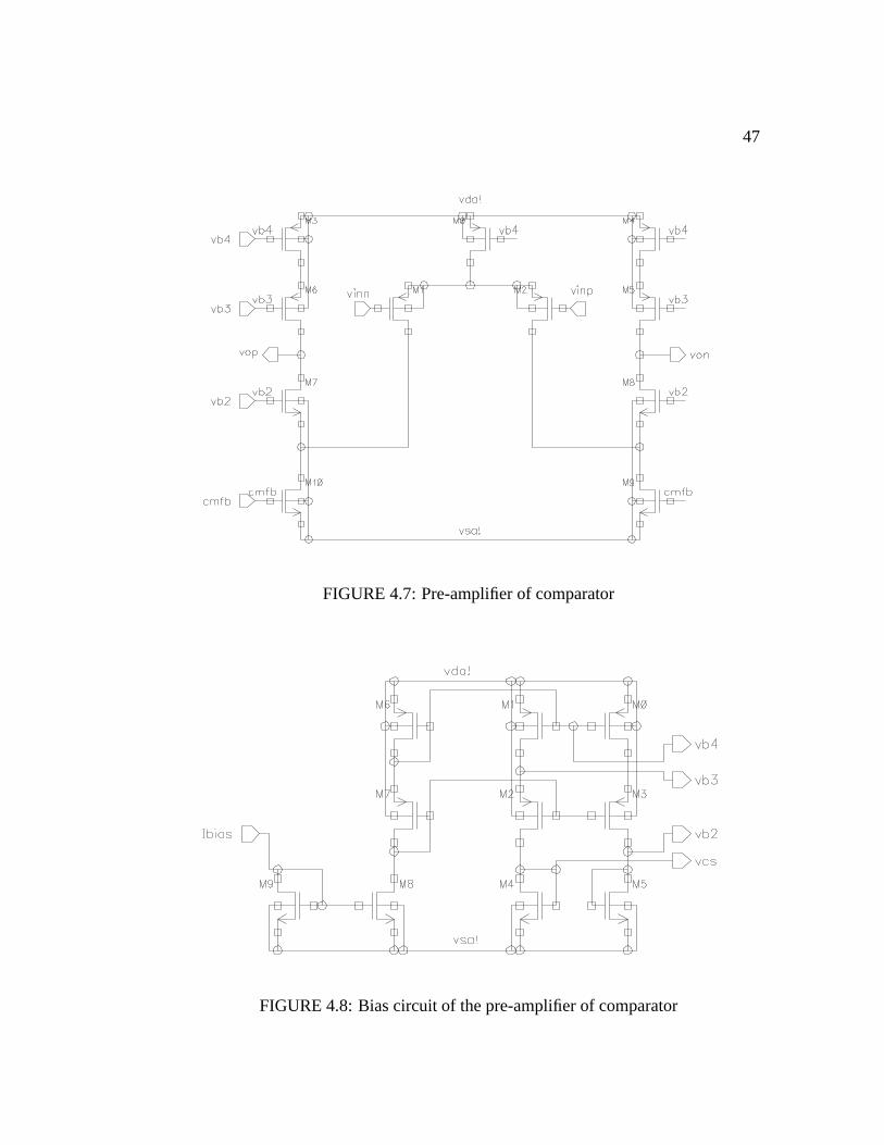
47
FIGURE 4.7: Pre-amplifier of comparator
FIGURE 4.8: Bias circuit of the pre-amplifier of comparator
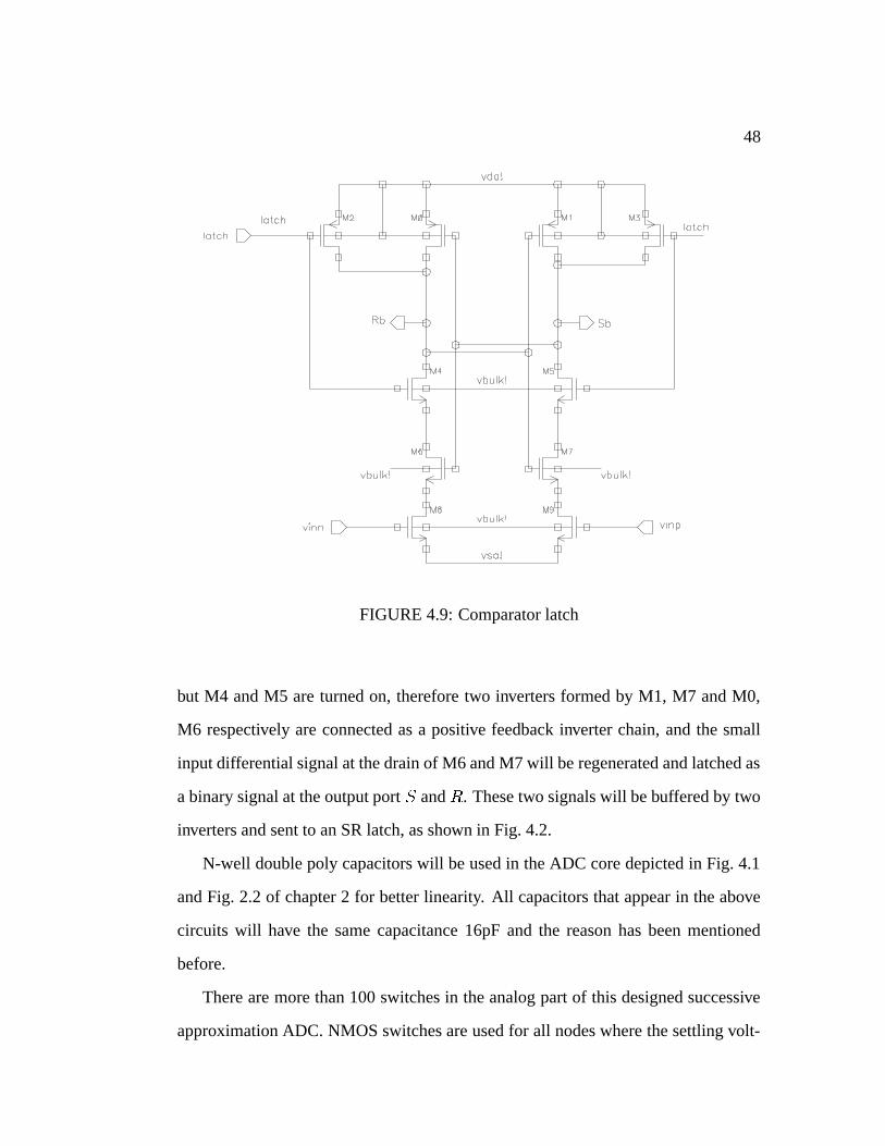
48
FIGURE 4.9: Comparator latch
but M4 and M5 are turned on, therefore two inverters formed by M1, M7 and M0,
M6 respectively are connected as a positive feedback inverter chain, and the small
input differential signal at the drain of M6 and M7 will be regenerated and latched as
a binary signal at the output port and . These two signals will be buffered by two
inverters and sent to an SR latch, as shown in Fig. 4.2.
N-well double poly capacitors will be used in the ADC core depicted in Fig. 4.1
and Fig. 2.2 of chapter 2 for better linearity. All capacitors that appear in the above
circuits will have the same capacitance 16pF and the reason has been mentioned
before.
There are more than 100 switches in the analog part of this designed successive
approximation ADC. NMOS switches are used for all nodes where the settling volt-
49
0 1 2 3 4 5 6 7 8 9 100
500
1000
1500
2000
2500
3000
3500
4000
Channel Width (µ m)
Sw
itch−
on R
esis
tanc
e (Ω
) at
Sig
nal V
olta
ge 0
.9V
FIGURE 4.10: NMOS switch-on resistance varies with switch size
0 0.2 0.4 0.6 0.8 1 1.2 1.4 1.6 1.80
500
1000
1500
2000
2500
Signal Voltage (V)
Sw
itch−
On
Res
ista
nce
(Ω)
0.5 µ
1.0µ
1.5µ
2.0µ
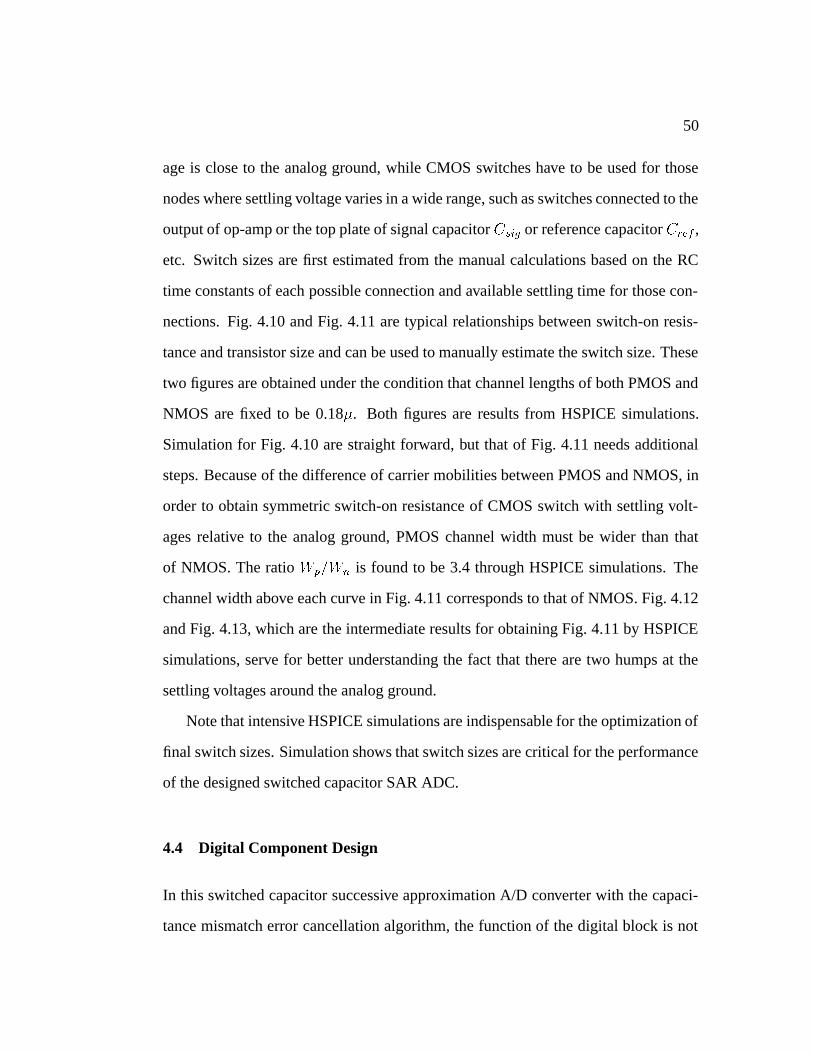
FIGURE 4.11: CMOS switch-on resistance with different switch sizes vary withsettling voltage
50
age is close to the analog ground, while CMOS switches have to be used for those
nodes where settling voltage varies in a wide range, such as switches connected to the
output of op-amp or the top plate of signal capacitor or reference capacitor ,
etc. Switch sizes are first estimated from the manual calculations based on the RC
time constants of each possible connection and available settling time for those con-
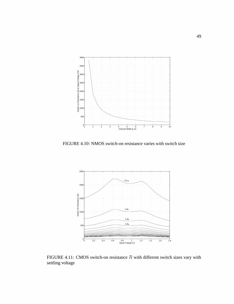
nections. Fig. 4.10 and Fig. 4.11 are typical relationships between switch-on resis-
tance and transistor size and can be used to manually estimate the switch size. These
two figures are obtained under the condition that channel lengths of both PMOS and
NMOS are fixed to be 0.18. Both figures are results from HSPICE simulations.
Simulation for Fig. 4.10 are straight forward, but that of Fig. 4.11 needs additional
steps. Because of the difference of carrier mobilities between PMOS and NMOS, in
order to obtain symmetric switch-on resistance of CMOS switch with settling volt-
ages relative to the analog ground, PMOS channel width must be wider than that
of NMOS. The ratio is found to be 3.4 through HSPICE simulations. The
channel width above each curve in Fig. 4.11 corresponds to that of NMOS. Fig. 4.12
and Fig. 4.13, which are the intermediate results for obtaining Fig. 4.11 by HSPICE
simulations, serve for better understanding the fact that there are two humps at the
settling voltages around the analog ground.
Note that intensive HSPICE simulations are indispensable for the optimization of
final switch sizes. Simulation shows that switch sizes are critical for the performance
of the designed switched capacitor SAR ADC.
4.4 Digital Component Design
In this switched capacitor successive approximation A/D converter with the capaci-
tance mismatch error cancellation algorithm, the function of the digital block is not

51
0 0.2 0.4 0.6 0.8 1 1.2 1.4 1.6 1.8 20
0.002
0.004
0.006
0.008
0.01
0.012
0.014
0.016
Signal Voltage (V)
g ds fo
r P
MO
S a
nd N
MO
S (
1/Ω
)
gdsn
gdsp
0.5µ
1.0µ 1.5µ
2.0µ
10.0µ
FIGURE 4.12: CMOS switch-on transconductances and
0 0.2 0.4 0.6 0.8 1 1.2 1.4 1.6 1.8 20
0.002
0.004
0.006
0.008
0.01
0.012
0.014
0.016
Signal Voltage (V)
g dsn +
gds
p for
CM
OS
(1/
Ω)
0.5µ 1.0µ 1.5µ
2.0µ
10.0µ
FIGURE 4.13: CMOS switch-on transconductance

52
only a clock generator that produces periodic non-overlap clock signals, but also a
finite state machine that produces the non-periodic sequential logic control signal to
realize the algorithm. The top level of the digital block is shown in Fig. 4.14.
Analog Input
Generator
Clock
Non-overlap Phases
Conversion Status Signals
State
Machine
Switch Control Signals
16 bits Parallel Output
Reset
External Clock
bit
Block
Analog
FIGURE 4.14: Top level of digital block relative to analog block of the SC SAR–ADC
4.4.1 Clock Generator
The timing diagram of all clock signals is shown in Fig. 4.15. Driven by the external
master clock, a two-phase non-overlap clock and are generated by circuit
introduced in [6]. Signal “clearF” starts the conversion of a new sample. This signal
is necessary to reset the flag of the state machine that traces the error charge free
capacitor, as described in chapter 2. At the beginning of each sample, the error free
capacitor must be reset to . Another function of signal “clearF” is to gate and
and generate and for predictive phase and actual sampling phase to sample
the input signal. Signal “Refresh” marks two phases of predictive CDS operation
of the LSB, which corresponds to phase ➀ in Fig. 4.1. Its invert signal “ ”
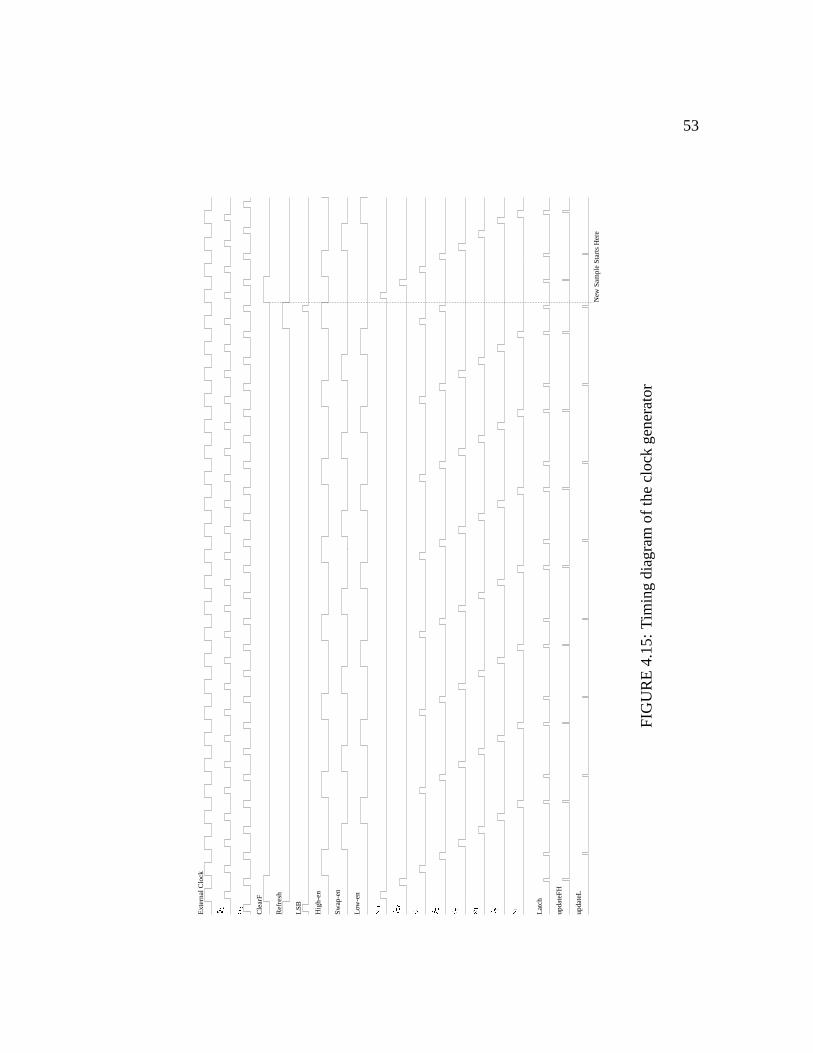
53
Ext
erna
lClo
ck
Cle
arF
Ref
resh
LSB
Hig
h-en
New
Sam
ple
Star
tsH
ere
Swap
-en
Low
-en
upda
teL
upda
teFH
Lat
ch
FIG
UR
E4.
15:
Tim
ing
diag
ram
ofth
ecl
ock
gene
rato
r
54
corresponds to phase ➁ in the same figure. Signal “LSB” is created by “Refresh” and
, which is necessary to discharge the relevant capacitors for preparing to sample
the next input signal. As shown in Fig. 4.15, each sample needs 23 external clock
periods, therefore a counter is needed.
MSB is generated by sampling phases and . Because of the operational
difference between sampling and normal conversion, these two phases are separated
from normal 6-phase conversion sequences. This leads to a non-periodic clock struc-
ture for through , as shown in Fig. 4.15, however, this reduces the number of
clocks needed for each sample. Otherwise 27 clocks are needed for each sample,
among them 3 clocks are wasted to maintain the periodic 6-phase clock structure.
In order to obtain the non-periodic 6-phase clock structure, 3 internal clock enve-
lope signals “High en”, “Swap en” and “Low en” are generated from the counter.
These envelope signals will be used to gate the normal non-overlap 2-phase clocks
and . Specifically, and are gated by “High en” to generate and , by
“Swap en” to generate and , by “Low en” to generate and .
“Latch” signal is generated at the end of phases , and for latching the
results of the comparator. After a short delay for binary signal regeneration in the
latch of Fig. 4.2, output “bit” of the comparator is updated either as the higher bit by
signal “updateFH” or the lower bit by signal “updateL”.
Conversion status signals “clearF”, “Refresh”, “LSB”, “Latch”, “updateFH” and
“updateL” may be directly used by switches in the analog block, while phase clock
signals , , , , , , and must be gated by state machine to generate
proper switch clocks for the algorithm discussed in chapter 2 and chapter 3. The state
machine is discussed in the following section.
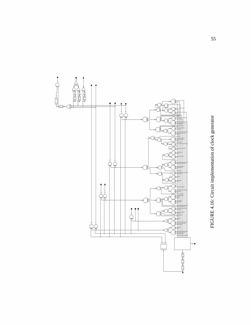
The circuit implementation of the clock generator is shown in Fig. 4.16.
55
FIG
UR
E4.
16:
Cir
cuit
impl
emen
tatio
nof
cloc
kge
nera
tor
56
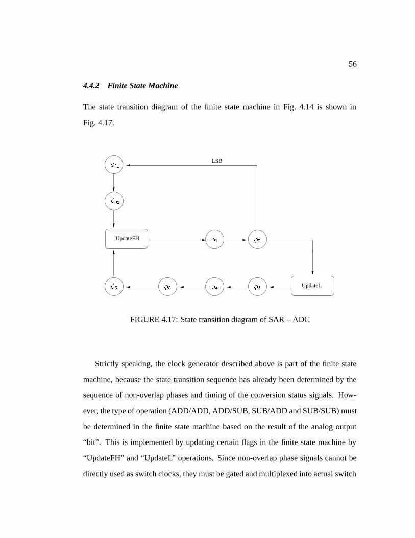
4.4.2 Finite State Machine
The state transition diagram of the finite state machine in Fig. 4.14 is shown in
Fig. 4.17.
UpdateL
LSB
UpdateFH
FIGURE 4.17: State transition diagram of SAR – ADC
Strictly speaking, the clock generator described above is part of the finite state
machine, because the state transition sequence has already been determined by the
sequence of non-overlap phases and timing of the conversion status signals. How-
ever, the type of operation (ADD/ADD, ADD/SUB, SUB/ADD and SUB/SUB) must
be determined in the finite state machine based on the result of the analog output
“bit”. This is implemented by updating certain flags in the finite state machine by
“UpdateFH” and “UpdateL” operations. Since non-overlap phase signals cannot be
directly used as switch clocks, they must be gated and multiplexed into actual switch
57
clocks by this finite state machine.
Circuit implementation of the state machine is shown in Fig. 4.18.
In order to eliminate signal dependent charge injection, switches connected to
the signal voltage dependent nodes should be closed after other switches are closed.
Therefore short delays are necessary for some switch signals after the finite state
machine.
4.5 Full Chip Simulation
Full chip simulations are performed during the design parameter optimizations. Since
there are a lot of transistors inside digital block, a full transistor level simulation,
which include both analog and digital components, will be too time consuming to be
implemented. Therefore the following approach is used. Digital block is first simu-
lated in the full transistor level by HSPICE. Once the correct control logic has been
verified by transistor level simulations, all gates in digital block will be represented
by proper verilog models. The full chip simulations are then performed by simulator
“spectreSVerilog” inside CADENCE. In simulations the numerical relative tolerance
is , voltage absolute tolerance and current absolute tolerance . The
final simulation result is shown in Fig. 4.19.

58
FIG
UR
E4.
18:
Cir
cuit
impl
emen
tatio
nof
stat
em
achi
ne

59
0 50 100 150 200 250 300 350 400 450 500−140
−120
−100
−80
−60
−40
−20
0
fs/2
Pow
er S
pect
rum
Den
sity
in D
B
SNR=89.3dB, SFDR=91.8dB
FIGURE 4.19: Output spectrum of the switched capacitor SAR – ADC by full chipsimulation
The layout of this chip with National Semiconductor CMOS9 process is shown
in Fig. 4.20.
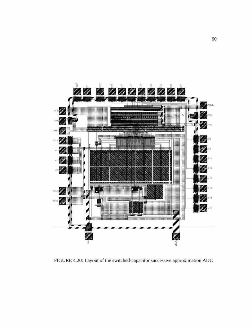
60
FIGURE 4.20: Layout of the switched-capacitor successive approximation ADC
61
Chapter 5
Summary and Future Work
5.1 Summary
The mismatch error canceling algorithm of the switched capacitor successive approx-
imation A/D converter has been improved. Compared to the original algorithm, the
finite state machine of the digital block for switch control is expanded because of the
tracing of the error charge free capacitor, but the error canceling operation becomes
more consistent.
The predictive correlated double sampling technique in the switched capacitor
successive approximation A/D converter was studied theoretically, which revealed
that normal predictive correlated double sampling technique is not adequate to achieve
high resolution SC SAR – ADC. The operational difference of predictive CDS in SC
SAR – ADC from that in other applications were explained. Based on the above
studies, a predictive CTS technique was proposed as an improvement of predictive
CDS in SC SAR – ADC, which was proved efficient by SWITCAP simulations.
A 1.8V switched capacitor SAR – ADC was designed with National Semicon-
ductor CMOS9 technology, which adopted results of above researches. The detailed
transistor level design and its layout were provided. Full chip simulation shows that
the design was successful, and this switched- capacitor ADC was fabricated.

62
5.2 Plan of Future Work
The test board of the designed SC SAR – ADC needs to be designed and fabricated
in order to test the performance of the designed chip. The improvement of this A/D
converter should eventually result in the application of a real product.
63
BIBLIOGRAPHY
[1] R. Adams, K. Nguyen, and K. Sweetland. “A 113 dB SNR Oversampling DACwith Segmented Noise-Shaped Scrambling”. In ISSCC Dig. Tech. Papers, pages62–63, Feb 1998.
[2] K. Haug, G. C. Temes, and K. Martin. “Improved Offset-CompensationSchemes for SC Circuits”. In Proceedings of IEEE International Symposiumon Circuit and Systems, pages 1054–1057, 1984.
[3] L. Hernandez. “Digital Implementation of Mismatch Shaping in OversampledPipeline A/D Converters”. Electron. Lett., vol.34(no.7):pp.616–617, Apr 1998.
[4] Y. Huang, G. C. Temes, and P. Ferguson, Jr. “Experimental Results on ReducedHarmonic Distortion with Correlated Double Sampling”. In Dig. of Symp. VLSICircuits, Jun 1998.
[5] Yunteng Huang. “Design Techniques of High-Performance Switched-CapacitorCircuits in the Presence of Component Imperfections”. PhD thesis, OregonState University, 1997.
[6] David Johns and Ken Martin. “Analog Integrated Circuit Design”. John Wiley& Sons, Inc., 1997.
[7] L. E. Larson and G. C. Temes. “SC Building Blocks with Reduced Sensitivityto Finite Amplifier Gain, Bandwidth and Offset Voltage”. In Proceedings ofIEEE International Symposium on Circuit and Systems, pages 334–338, 1987.
[8] C. C. Lee. “A New Switched-Capacitor Realization for Cyclic Analog-to-Digital Converter”. In Proceedings of IEEE International Symposium on Circuitand Systems, pages 1261–1265, Newport Beach, CA, USA, May 1983.
[9] P. W. Li, M. J. Chin, P. R. Gray, and R. Castello. “A Ratio-Independent Algo-rithmic Analog-to-Digital Conversion Technique”. IEEE Journal of Solid-StateCircuits, vol.19(no.6):pp.828–836, Dec 1984.
[10] K. W. Martin. “A High-Speed, High-Accuracy Pipelined A/D Converter”. InIEEE 15th Asilomar Conf. on Circuits, Systems, and Computers, Nov 1981.
[11] R. H. McCharles, V. A. Saletore, W. C. Black, Jr., and D. A. Hodges. “AnAlgorithmic Analog-to-Digital Converter”. In Int. Solid-State Circuits Conf.,pages 96–97, Philadelphia,PA,USA, Feb 1977.
64
[12] K. Nagaraja, K. Singhal, T. R. Viswanathan, and J. Vlach. “SC Circuits withReduced Sensitivity to Finite Amplifier Gain”. In Proceedings of IEEE Inter-national Symposium on Circuit and Systems, pages 618–621, 1986.
[13] Steven R. Norsworthy, Richard Schreier, and Gabor C. Temes. “Delta-SigmaData Converters – Theory, Design, and Simulation”. IEEE Press, 1997.
[14] Hidetoshi Onodera, Tetsuo Takeishi, and Keikichi Tamaru. “A Cyclic A/DConverter That Does Not Require Ratio-Matched Components”. IEEE Journalof Solid-State Circuits, vol.23(no.1):pp.152–158, Feb 1988.
[15] Vincenzo Peluso, Michiel Steyaert, and Willy Sansen. “Design of Low-VoltageLow-Power CMOS Delta-Sigma A/D Converters”. Kluwer Academic Publish-ers, Boston, 1999.
[16] Shahriar Rabii and Bruce A. Wooley. “A 1.8-V digital-audio sigma-delta modulator in 0.8- CMOS”. IEEE Journal of Solid-State Circuits,vol.32(no.6):pp.783–796, Jun 1997.
[17] B. Razavi. “Principle of Data Conversion System Design”. IEEE Press, 1995.
[18] P. Rombouts and L. Weyten. “A Digital Error-Averaging Technique forPipelined A/D Conversion”. IEEE Transactions on Circuits and Systems II,vol.45(no.9):pp.1321–1323, Sep 1998.
[19] R. Schreier and B. Zhang. “Noise-Shaped Multibit D/A Converter EmployingUnit Elements”. Electron. Lett., vol.31(no.20):pp.1712–1713, Sep 1995.
[20] C. C. Shih and P. R. Gray. “Reference Refreshing Cyclic Analog-to-Digital andDigital-to-Analog Converters”. IEEE Journal of Solid-State Circuits, vol.SC-21:pp.544–554, Aug 1986.
[21] Tao Sun. “Compensation Techniques for Cascaded Delta-Sigma A/D Convert-ers and High-Performance Switched-Capacitor Circuits”. PhD thesis, OregonState University, 1998.
[22] G. Temes, Y. Huang, and P. Ferguson, Jr. “A High-Frequency Track-and-HoldStage with Offset and Gain Compensation”. IEEE Trans. Circuits and Systems- II, vol.42(no.8):pp.559–561, Aug 1995.
[23] K. Watanabe and H. Matsumoto. “Switched-Capacitor Algorithmic Digital-to-Analog and Analog-to-Digital Converters”. In Proceedings of IEEE Interna-tional Symposium on Circuit and Systems, pages 331–332, Kyoto, Japan, May1985.
[24] H. Yoshizawa, Y. Huang, and G.C. Temes. “Improved SC Amplifier with LowSensitivity to Op-amp Imperfections”. Electron. Lett., vol.33(no.5):pp.348–349, Feb 1997.
65
[25] Zhiliang Zheng. “Low Power High Resolution Data Converter in Digital CMOSTechnology”. Master’s thesis, Oregon State University, 1999.
[26] Zhiliang Zheng, Byung-Moo Min, Un-Ku Moon, and Gabor C. Temes. “Ef-ficient Error-Cancelling Algorithmic ADC”. In Proceedings of IEEE Interna-tional Symposium on Circuit and Systems, Geneva, Switzerland, May 2000.
[27] Zhiliang Zheng, Un-Ku Moon, Jesper Steensgaard, Bo Wang, and Gabor C.Temes. “Capacitor Mismatch Cancellation Technique for A Seccessive Aprox-imation A/D Converter”. In Proceedings of IEEE International Symposium onCircuit and Systems, volume vol. 2 of 6, pages II–326–329, May 1999.
Recommended