Electrostatic Field Solver Capable of HandlingDielectrics
A Project Report
Submitted in partial fulfilment of the
requirements for the Degree of
Master of Technology
in
Computational Science
by
Abhishek Kolipaka
Supercomputer Education and Research Centre
Indian Institute of Science
BANGALORE – 560 012
July 13, 2011

i
c©Abhishek Kolipaka
July 13, 2011
All rights reserved

Dedicated to
My Parents
and
all my well–wishers...
Acknowledgements
During my stay at IISc, I have met many wonderful people who finally have become an
integral part of my professional and personal life. I take this opportunity to thank all
those people. Their help, support and guidance, have been invaluable for me.
I thank my project guide Dr. A. K. Mohanty. His problem solving approach accom-
panied with knowledge base and commitment has been a great source of inspiration for
me. Under his guidance not only I have completed my project work, but have also learnt
much which will help me in my future academic and professional life.
I am grateful to Prof. R. Govindrajan, Chairman, Supercomputer Education and
Research Centre , for allowing me to use all the facilities of the department. I also thank
all the faculty and staff members of the department for their assistance.
I would thank my friends Vinay Kumar, Appala Naidu, Sharath, Anwit Roy, and
Vaibhav. I will always cherish their friendship. My interaction with them has taught
me many principles of life. Last but not the least, I would like to render my sincere
gratitude to all those who have directly or indirectly helped in making this happen.
i
Abstract
The aim of the project is to implement a electrostatic 3D BEM package which can be
used in the presence of dielectrics and conductors. This package can be used to deter-
mine electric field and potential at any point in space. It also helps in the visualization
of equipotential surfaces and electric field lines. Its applications include the study of
ion traps. The package allows convenient input specification for the conductors and di-
electrics. The shapes of the electrodes are specified using parametric equations for the
surfaces. For the dielectrics the direction of the outward normal is also specified. On
the conducting electrodes potentials are specified, while for the dielectrics the relative
permittivities are specified.
In addition to fully three-dimensional problems, the package can also solve problems
with axial or two-dimensional geometries. For problems with axial or two-dimensional
symmetries it provides simpler electrode specification and more economical field evalua-
tion.
The package developed has been tested on problems for which analytical results
are known, and the numerical results obtained with BEM are compared with analytical
results to test the accuracy of package. It has been used in the study of various ion traps
including a planar toroidal trap.
ii
Contents
Acknowledgements i
Abstract ii
Keywords v
Notation and Abbreviations vi
1 Introduction 1
1.1 Boundary Element Method . . . . . . . . . . . . . . . . . . . . . . . . . . 11.2 Polarization . . . . . . . . . . . . . . . . . . . . . . . . . . . . . . . . . . 21.3 Electrostatic boundary conditions . . . . . . . . . . . . . . . . . . . . . . 2
2 Methodology 4
2.1 Steps for BEM . . . . . . . . . . . . . . . . . . . . . . . . . . . . . . . . 42.2 2D problem . . . . . . . . . . . . . . . . . . . . . . . . . . . . . . . . . . 62.3 3D problem . . . . . . . . . . . . . . . . . . . . . . . . . . . . . . . . . . 72.4 Axially symmetric 3D problem . . . . . . . . . . . . . . . . . . . . . . . . 92.5 Electric field lines . . . . . . . . . . . . . . . . . . . . . . . . . . . . . . . 12
3 Analtical Solution 14
3.1 Sphere . . . . . . . . . . . . . . . . . . . . . . . . . . . . . . . . . . . . . 143.2 Cylinder . . . . . . . . . . . . . . . . . . . . . . . . . . . . . . . . . . . . 143.3 Uniform electric field . . . . . . . . . . . . . . . . . . . . . . . . . . . . . 15
4 Testcases and results 16
4.1 2D problem . . . . . . . . . . . . . . . . . . . . . . . . . . . . . . . . . . 164.2 3D problem . . . . . . . . . . . . . . . . . . . . . . . . . . . . . . . . . . 174.3 Axially symmetric 3D problem . . . . . . . . . . . . . . . . . . . . . . . . 19
5 Conclusions and Future work 25
5.1 Conclusions . . . . . . . . . . . . . . . . . . . . . . . . . . . . . . . . . . 255.2 Future work . . . . . . . . . . . . . . . . . . . . . . . . . . . . . . . . . . 25
References 26
iii
List of Figures
1.1 Electric field at the boundary between two dielectric . . . . . . . . . . . 3
2.1 Electric field components at the dielectric element i . . . . . . . . . . . . 52.2 Division of boundary into strips . . . . . . . . . . . . . . . . . . . . . . . 72.3 Division of boundary into strips . . . . . . . . . . . . . . . . . . . . . . . 82.4 Dimensions of triangle . . . . . . . . . . . . . . . . . . . . . . . . . . . . 92.5 Axially symmetric 3D objects . . . . . . . . . . . . . . . . . . . . . . . . 92.6 2D representation of 3D axially symmetric objects in ρ - z plane . . . . . 102.7 Field line plot of planar toroidal trap in X-Z plane . . . . . . . . . . . . . 132.8 Field lines plot of sphere kept between two parallel disks in X-Z plane . . 13
4.1 Cylinder kept between conducting plates . . . . . . . . . . . . . . . . . . 164.2 Numerical and analytical electric fields at the center of dielectric cylinder
for various dielectric constants in division into strips . . . . . . . . . . . . 174.3 Error between numerical and analytical electric fields at the center of
dielectric cylinder for various dielectric constants in division into strips . 184.4 Dielectric sphere kept between conducting plates . . . . . . . . . . . . . . 194.5 Numerical and analytical electric fields at the center of dielectric sphere
for various dielectric constants in triangular meshing . . . . . . . . . . . 204.6 Error between numerical and analytical electric fields at the center of
dielectric sphere for various dielectric constants in triangular meshing . . 214.7 Error between numerical and analytical electric fields at the center of
dielectric sphere for various step sizes of dielectric in triangular meshing . 224.8 Dielectric sphere kept between conducting disks . . . . . . . . . . . . . . 224.9 Numerical and analytical electric field at the center of dielectric sphere for
various dielectric constants in ring meshing . . . . . . . . . . . . . . . . . 234.10 Error between numerical and analytical electric field at the center of di-
electric sphere for various dielectric constants in ring meshing . . . . . . 234.11 Numerical and analytical electric field at the center of dielectric sphere for
various step sizes of dielectric in ring meshing . . . . . . . . . . . . . . . 24
iv
Notation and Abbreviations
BVP - Boundary Value Problem.
BEM - Boundary Element Method.
FEM - Finite Element Method.
FDM - Finite Difference Method.
2D - Two Dimensional.
3D - Three Dimensional.
v
Chapter 1
Introduction
1.1 Boundary Element Method
BVP is a problem in which some data is given on the boundary B we need to solve the
problem in boundary B and domain D. Since boundary value problem always does not
have closed form solution due to various complexities, so some numerical techniques are
followed to solve boundary value problem numerically, such as finite element method,
finite difference method, and boundary element method. These methods are different
discretizations of different formulations of identical boundary value problem.
Boundary value problem can be represented in different formulations such as differ-
ential formulation, integral formulation and boundary integral formulation. Differential
formualtion is obtained when local view is adopted and integral formulation is obtained
when global view is adopted. Boundary integral formulation is obtained from tranfor-
mation of differntial formualtion. Differential formulation is called as strong formulation
and integral formulation is called as weak formulation.Boundary element method is a
powerful numerical techinque this is obtained by discretization of boundary value prob-
lem in boundary integral formulation.
In BEM we approximate the solution to a PDE by looking at the solution to the
PDE on the boundary and then use that information to find the solution inside the do-
main. BEM needs descretization only on boundary where as FEM needs descretization
1
Chapter 1. Introduction 2
on entire domain so BEM is very useful incase of infinite boundary problems. Matrix
obtained from BEM are small and dense where as matrix obtained from FEM are large
and sparse. In elecrostatic PDE needs to be solved is Laplace equation subjected to
given boundary conditions.
1.2 Polarization
Dielectric is a material in which all charges are tightly attached to atoms or molecules
they can move only a bit within atom or molecule. Cumulative effects of this microscopic
displacements gives properties of dielectrics. When an atom is placed in electric field
although atom is neutral electrically, but there positive nucleus at center and negative
electron cloud surrounding the atom, due to presence of electric field nucleus is pulled in
the direction of electric field and electron cloud is pushed in the opposite direction, this
creates a small electric dipole is induced on atom, this phenomenon is called stretching.
If electric field strength is sufficiently large it can remove electrons from atom causing
ionization of atom. In some molecules there is built in permanent dipole moment such as
water molecule. When such molecules are placed in electric field this dipoles gets rotated
and alligned in the direction of electric field, this phenomenon is called rotation. When a
dielectric is placed in electric field due to stretching and rotation all microscopic dipoles
points in the direction of electric field and dielectric becomes polarized this phenomenon
is called polorization.
1.3 Electrostatic boundary conditions
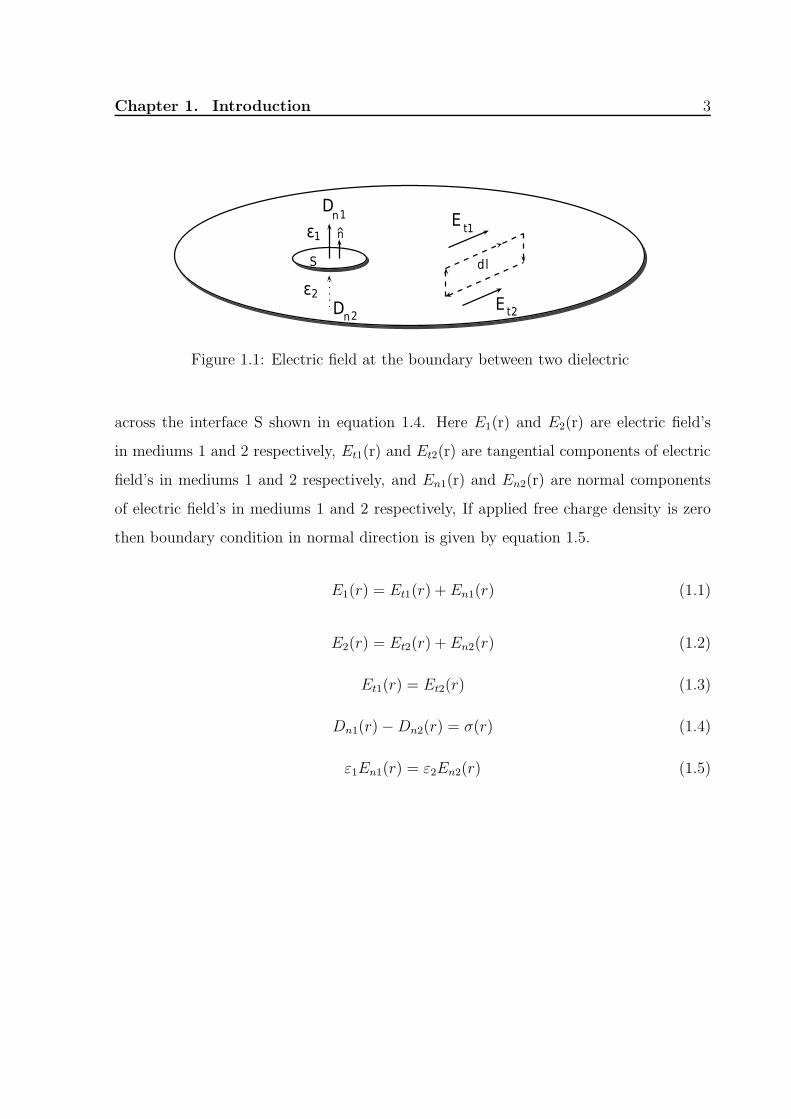
As shown in fig1.1, S is the interface separating two dielectrics with permitivites ε1
and ε2 at any point r belongs to S the electric field vector can be decomposed into
tangential Et(r) and normal En(r) components. The tangential component of electric
field is contiuous across the the interface S shown in equation 1.3. Normal component
of electric displacement (D = εE) is discontinuous by applied surface charge density
Chapter 1. Introduction 3
Figure 1.1: Electric field at the boundary between two dielectric
across the interface S shown in equation 1.4. Here E1(r) and E2(r) are electric field’s
in mediums 1 and 2 respectively, Et1(r) and Et2(r) are tangential components of electric
field’s in mediums 1 and 2 respectively, and En1(r) and En2(r) are normal components
of electric field’s in mediums 1 and 2 respectively, If applied free charge density is zero
then boundary condition in normal direction is given by equation 1.5.
E1(r) = Et1(r) + En1(r) (1.1)
E2(r) = Et2(r) + En2(r) (1.2)
Et1(r) = Et2(r) (1.3)
Dn1(r)−Dn2(r) = σ(r) (1.4)
ε1En1(r) = ε2En2(r) (1.5)
Chapter 2
Methodology
2.1 Steps for BEM
Data required for BEM computaion are boundary of electrodes, applied potential on
electrodes, boundary of dielectric, normals to the boundary of dielectric, and dielectric
constant. Boundary of electrodes, boundary of dielectric and normals to the boundary
of dielectric are given in parametric form. Since in 3D boundary is surface we need
two parameters to represent the boundary. By applying meshing technique boundary is
divided into basic elements. Different kinds of meshing techniques gives different kinds
of basic elements.
When potential is applied on conductor charge gets devoloped on conductor. To
satisfy electrostatic boundary conditions boundary of dielectric is replaced by charge, to
obtain all the charges Green’s matrix is solved. Green’s matrix is generated from set
of equations obtained by appying boundary conditions such as, for conductors potential
on basic element due to all elements is equal to applied potential. for dielectric ratio of
normal component of electric field inside the dielectric to normal component of electric
field outside the dielectric is equal to dielectric constant. Surface charge density on each
element is assumed to be constant.
Boundary condition on conductor element i can be represented by equation 2.1. Here
Gij is the potential at conductor element i due to unit charge on element j. Gii is
4

Chapter 2. Methodology 5
potential at center of element i due to element i. Vi is applied potential on conductor
element i. qi is charge on element i. qj is charge on element j. NC is the number of basic
elements on all conductors and ND is the number of basic elements on all the dielectrics.
Since there are only NC conductor elements so there will be only NC equations of this
kind.
Giiqi +NC+ND∑
j=1,j 6=i
Gijqj = Vi i = 1 . . .NC (2.1)
Figure 2.1: Electric field components at the dielectric element i
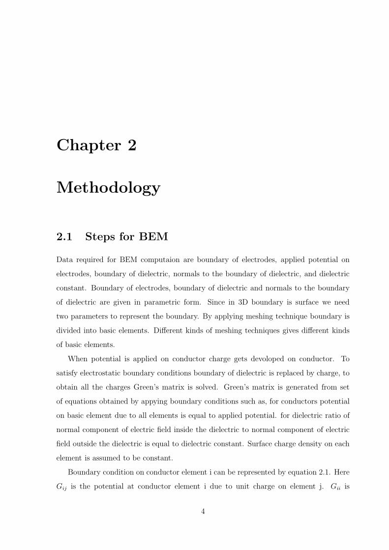
At any dielectric element i electric field can be represented as shown in fig 2.1. Here Ei
is electric field produced by dielectric element i, and n is the unit vector perpendicular to
to the element i having direction from inside the dielectric towards ouside the dielectric.
Einc is the electric field due to all elements along n direction. When boundary condition
is applied on the boundary of dielectric element i it will give equation 2.2.
Ei +1− εr
1 + εrEinc = 0 (2.2)
Chapter 2. Methodology 6
Einc can be written interms of equation 2.3. Here ~Γij is electric field at the center of
dielectric element i due to unit charge at the center of element j. Ei can be written in
terms of equation 2.4, Here Γii electric field at the center of element i due to unit charge
at element i. εr is the dielectric constant of dielectric element i.
Einc =NC+ND∑
j=1,j 6=i
(~Γij .n)qj (2.3)
Ei = Γiiqi (2.4)
Since there are only ND dielectric elements we will get only ND such equations. All
these ND can be represented as equation 2.5. Totally we will get NC + ND equations
which are solved to get charge distibution on boundary of conductors and boundary
of dielectric. Different meshing techniques which are studied are division into strips,
triangular meshing and ring meshing.
Γiiqi +(
1− εr
1 + εr
)NC+ND∑
j=1,j 6=i
(~Γij .n)qj = 0 i = 1 . . .ND (2.5)
2.2 2D problem
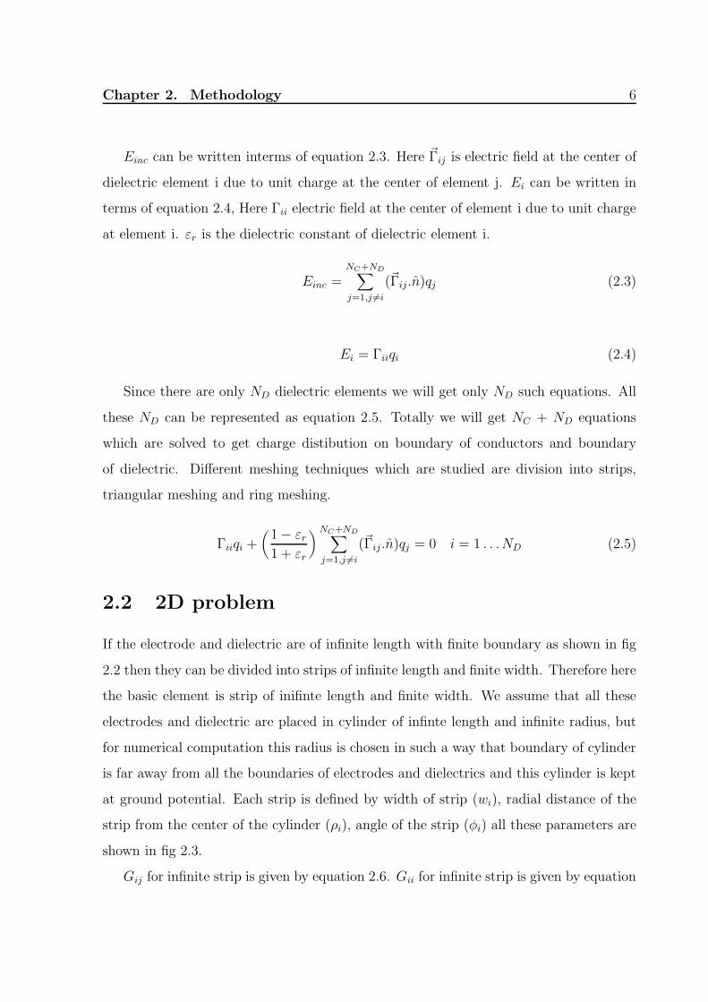
If the electrode and dielectric are of infinite length with finite boundary as shown in fig
2.2 then they can be divided into strips of infinite length and finite width. Therefore here
the basic element is strip of inifinte length and finite width. We assume that all these
electrodes and dielectric are placed in cylinder of infinte length and infinite radius, but
for numerical computation this radius is chosen in such a way that boundary of cylinder
is far away from all the boundaries of electrodes and dielectrics and this cylinder is kept
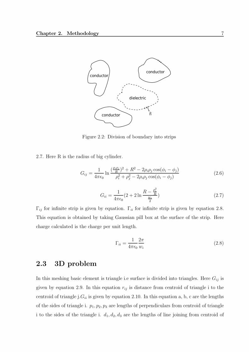
at ground potential. Each strip is defined by width of strip (wi), radial distance of the
strip from the center of the cylinder (ρi), angle of the strip (φi) all these parameters are
shown in fig 2.3.
Gij for infinite strip is given by equation 2.6. Gii for infinite strip is given by equation
Chapter 2. Methodology 7
Figure 2.2: Division of boundary into strips
2.7. Here R is the radius of big cylinder.
Gij =1
4πǫ0ln
(ρiρjR
)2 + R2 − 2ρiρj cos(φi − φj)
ρ2i + ρ2j − 2ρiρj cos(φi − φj)(2.6)
Gii =1
4πǫ0(2 + 2 ln
R−ρ2i
Rwi
2
) (2.7)
Γij for infinite strip is given by equation. Γii for infinite strip is given by equation 2.8.
This equation is obtained by taking Gaussian pill box at the surface of the strip. Here
charge calculated is the charge per unit length.
Γii =1
4πǫ0
2π
wi
(2.8)
2.3 3D problem
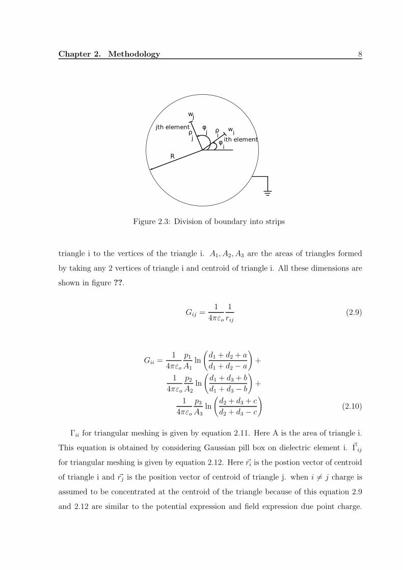
In this meshing basic element is triangle i.e surface is divided into triangles. Here Gij is
given by equation 2.9. In this equation rij is distance from centroid of triangle i to the
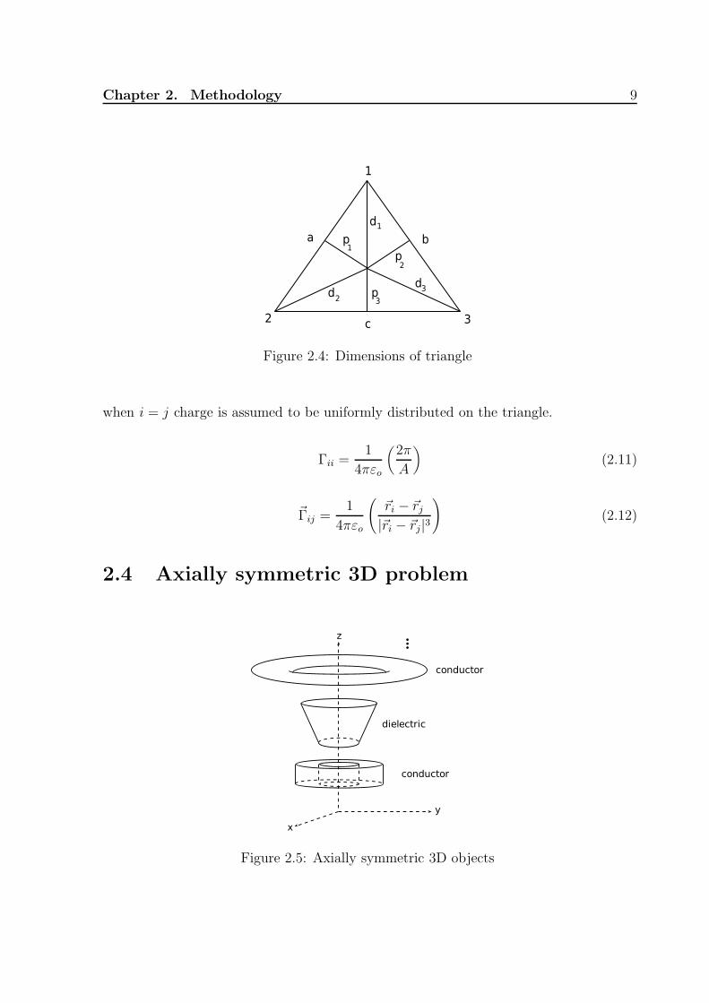
centroid of triangle j.Gii is given by equation 2.10. In this equation a, b, c are the lengths
of the sides of triangle i. p1, p2, p3 are lengths of perpendiculars from centroid of triangle
i to the sides of the triangle i. d1, d2, d3 are the lengths of line joining from centroid of
Chapter 2. Methodology 8
Figure 2.3: Division of boundary into strips
triangle i to the vertices of the triangle i. A1, A2, A3 are the areas of triangles formed
by taking any 2 vertices of triangle i and centroid of triangle i. All these dimensions are
shown in figure ??.
Gij =1
4πεo
1
rij(2.9)
Gii =1
4πεo
p1
A1
ln
(
d1 + d2 + a
d1 + d2 − a
)
+
1
4πεo
p2
A2
ln
(
d1 + d3 + b
d1 + d3 − b
)
+
1
4πεo
p3
A3
ln
(
d2 + d3 + c
d2 + d3 − c
)
(2.10)
Γii for triangular meshing is given by equation 2.11. Here A is the area of triangle i.
This equation is obtained by considering Gaussian pill box on dielectric element i. ~Γij
for triangular meshing is given by equation 2.12. Here ~ri is the postion vector of centroid
of triangle i and ~rj is the position vector of centroid of triangle j. when i 6= j charge is
assumed to be concentrated at the centroid of the triangle because of this equation 2.9
and 2.12 are similar to the potential expression and field expression due point charge.
Chapter 2. Methodology 9
Figure 2.4: Dimensions of triangle
when i = j charge is assumed to be uniformly distributed on the triangle.
Γii =1
4πεo
(
2π
A
)
(2.11)
~Γij =1
4πεo
(
~ri − ~rj
|~ri − ~rj|3
)
(2.12)
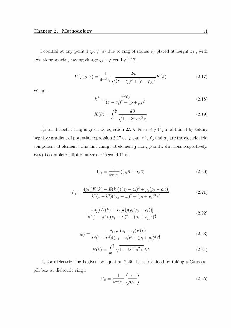
2.4 Axially symmetric 3D problem
Figure 2.5: Axially symmetric 3D objects
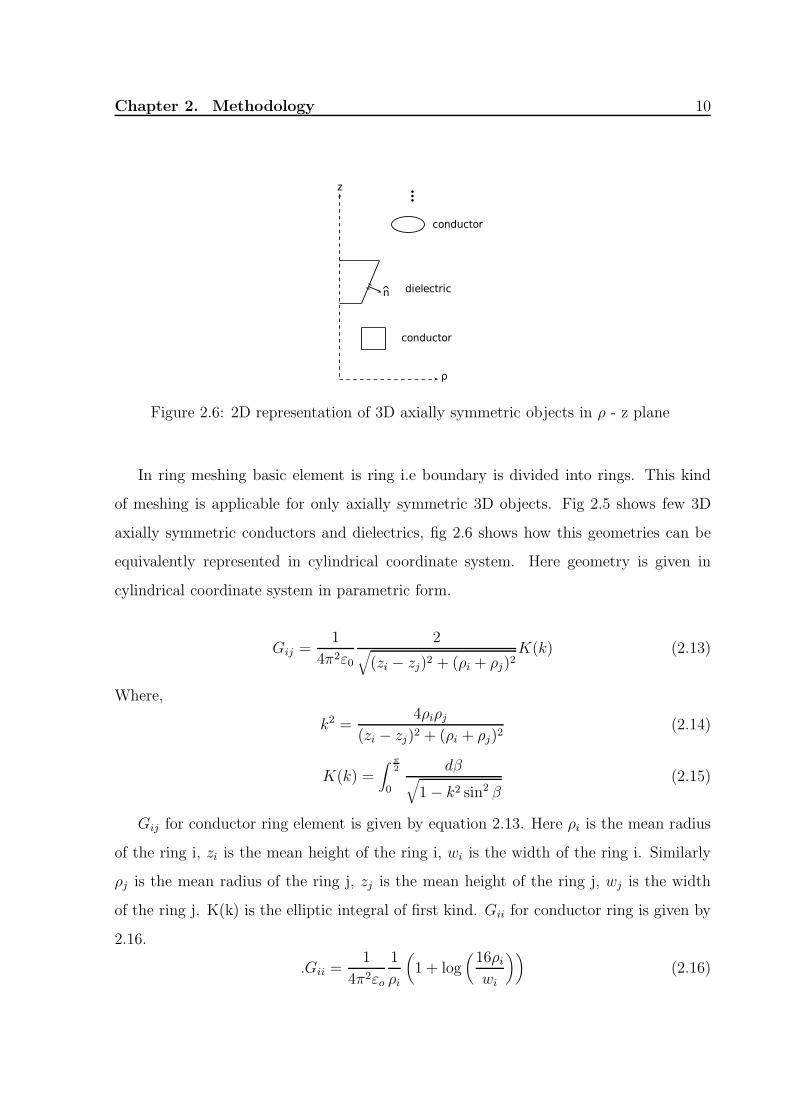
Chapter 2. Methodology 10
Figure 2.6: 2D representation of 3D axially symmetric objects in ρ - z plane
In ring meshing basic element is ring i.e boundary is divided into rings. This kind
of meshing is applicable for only axially symmetric 3D objects. Fig 2.5 shows few 3D
axially symmetric conductors and dielectrics, fig 2.6 shows how this geometries can be
equivalently represented in cylindrical coordinate system. Here geometry is given in
cylindrical coordinate system in parametric form.
Gij =1
4π2ε0
2√
(zi − zj)2 + (ρi + ρj)2K(k) (2.13)
Where,
k2 =4ρiρj
(zi − zj)2 + (ρi + ρj)2(2.14)
K(k) =∫ π
2
0
dβ√
1− k2 sin2 β(2.15)
Gij for conductor ring element is given by equation 2.13. Here ρi is the mean radius
of the ring i, zi is the mean height of the ring i, wi is the width of the ring i. Similarly
ρj is the mean radius of the ring j, zj is the mean height of the ring j, wj is the width
of the ring j. K(k) is the elliptic integral of first kind. Gii for conductor ring is given by
2.16.
.Gii =1
4π2εo
1
ρi
(
1 + log(
16ρiwi
))
(2.16)
Chapter 2. Methodology 11
Potential at any point P(ρ, φ, z) due to ring of radius ρj placed at height zj , with
axis along z axis , having charge qj is given by 2.17.
V (ρ, φ, z) =1
4π2ε0
2qj√
(z − zj)2 + (ρ+ ρj)2K(k) (2.17)
Where,
k2 =4ρρj
(z − zj)2 + (ρ+ ρj)2(2.18)
K(k) =∫ π
2
0
dβ√
1− k2 sin2 β(2.19)
~Γij for dielectric ring is given by equation 2.20. For i 6= j ~Γij is obtained by taking
negative gradient of potential expression 2.17 at (ρi, φi, zi), fij and gij are the electric field
component at element i due unit charge at element j along ρ and z dirctions respectively.
E(k) is complete elliptic integral of second kind.
~Γij =1
4π2εo(fij ρ+ gij z) (2.20)
fij =4ρj [(K(k)− E(k))((zj − zi)
2 + ρj(ρj − ρi))]
k2(1− k2)((zj − zi)2 + (ρi + ρj)2)5
2
(2.21)
−4ρj [(K(k) + E(k))(ρi(ρj − ρi))]
k2(1− k2)((zj − zi)2 + (ρi + ρj)2)5
2
(2.22)
gij =−8ρiρj(zj − zi)E(k)
k2(1− k2)((zj − zi)2 + (ρi + ρj)2)5
2
(2.23)
E(k) =∫ π
2
0
√
1− k2 sin2 βdβ (2.24)
Γii for dielectric ring is given by equation 2.25. Γii is obtained by taking a Gaussian
pill box at dielectric ring i.
Γii =1
4π2ε0
(
π
ρiwi
)
(2.25)
Chapter 2. Methodology 12
2.5 Electric field lines
One of the uses of this simulator is visualization of electric field lines, to get the electric
field lines the required data given by the user is boundary in which field lines needs to
be plotted, number of divisions along each boundary, termination criteria, and step size.
Each boundary is divided into number of divisions specified by the user to get the points
on the boundary, plotting of electric field lines starts from the points on the boundary.
At first a point on the boundary is taken and electric field is calculated at that
point, and the next point is obtained by moving distance of step size in the electric field
direction, if this next point lies in the boundary then this process is repeated, if this
next point lies out of the boundary then process is terminated, and the same process is
started from next boundary point and this whole process is done for all the boundary
points, all these points obtained are stored in a file and plotted to get electric field lines.
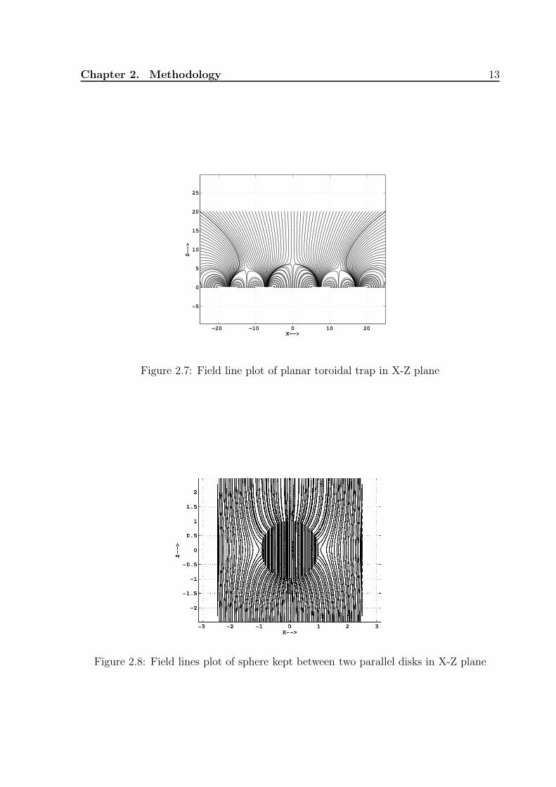
Fig 2.7 shows electric field lines of planar toroidal trap , on X-Z planes with the trap
kept on X-Y plane, since this is an axially symmetric structure electric field line graph
along any plane passing through Z axis will be same, by looking at the field lines we can
see approximately where the electric field is zero, this is approximate trapping point and
this is useful to give as initial point in the searching for exact trapping point.
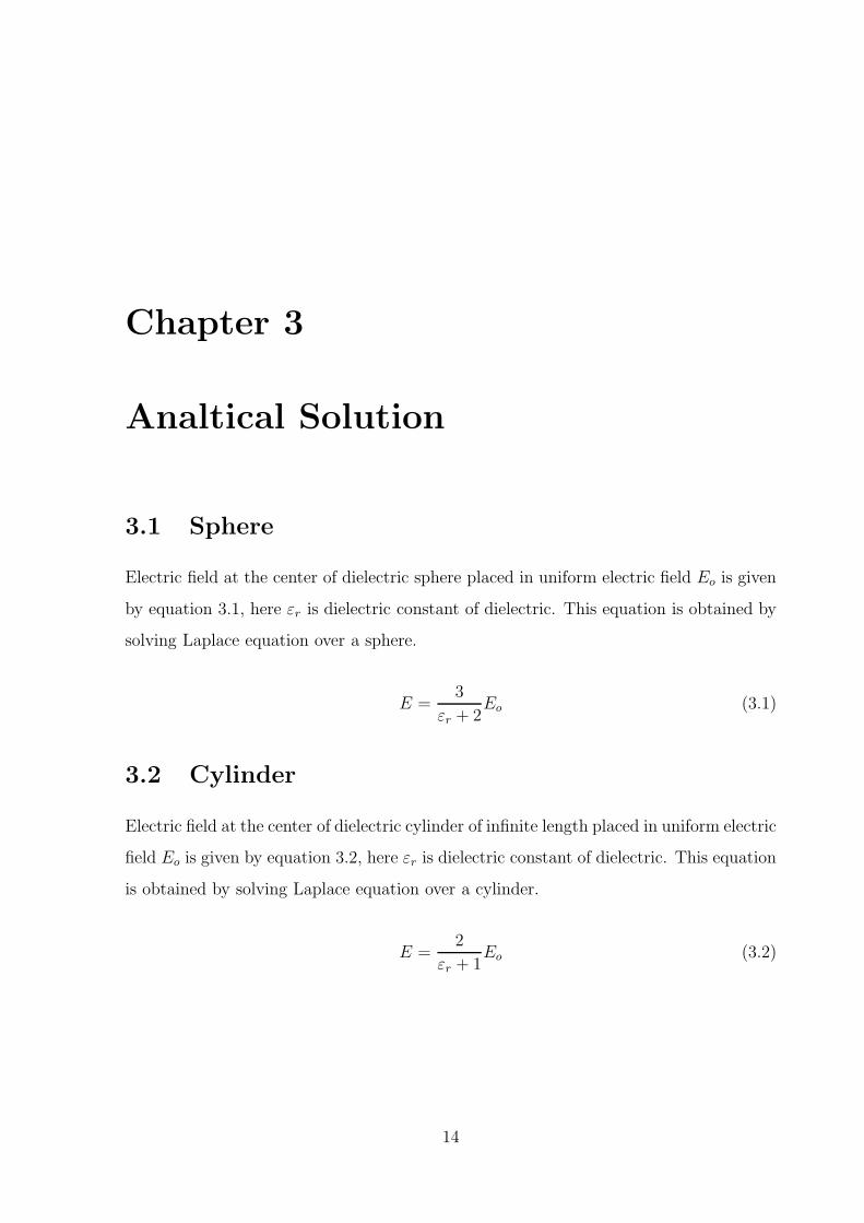
Fig 2.8 shows electric field lines of dielectric sphere kept between two parallel circular
disks with axis of sphere and disks along Z axis and graph is plotted in X-Z plane.
Chapter 2. Methodology 13
−20 −10 0 10 20
−5
0
5
10
15
20
25
X−−>
Z−
−>
Figure 2.7: Field line plot of planar toroidal trap in X-Z plane
Figure 2.8: Field lines plot of sphere kept between two parallel disks in X-Z plane
Chapter 3
Analtical Solution
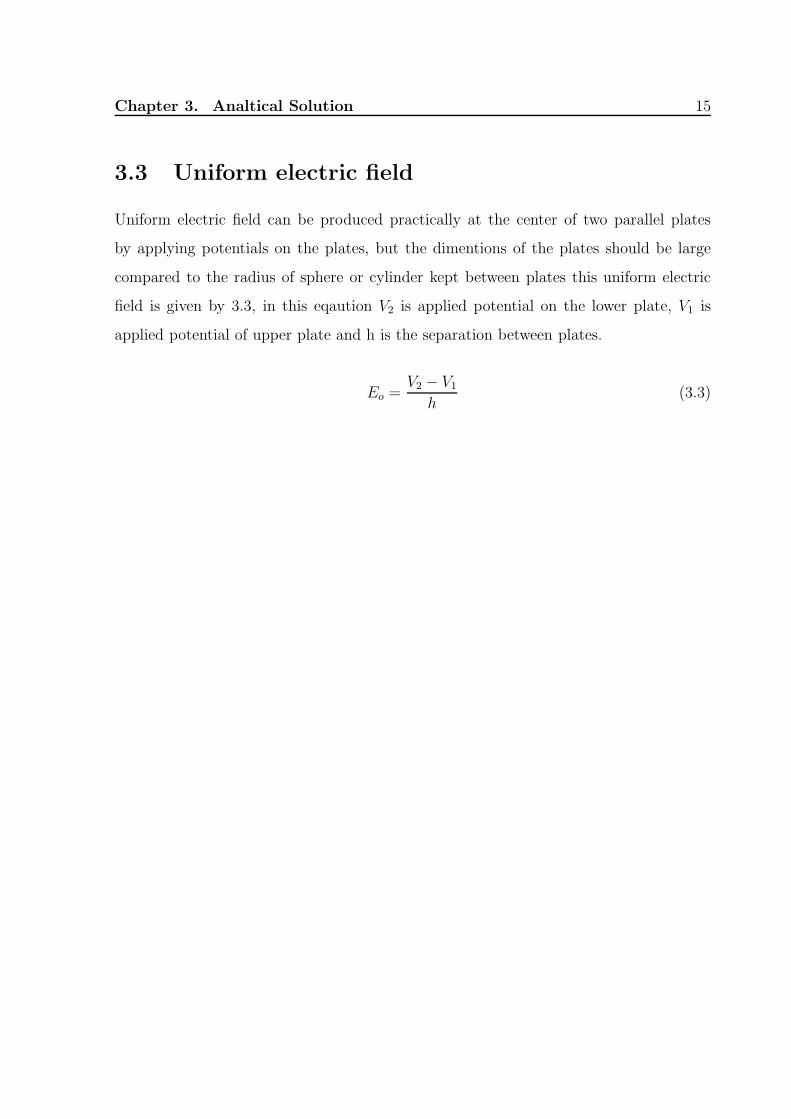
3.1 Sphere
Electric field at the center of dielectric sphere placed in uniform electric field Eo is given
by equation 3.1, here εr is dielectric constant of dielectric. This equation is obtained by
solving Laplace equation over a sphere.
E =3
εr + 2Eo (3.1)
3.2 Cylinder
Electric field at the center of dielectric cylinder of infinite length placed in uniform electric
field Eo is given by equation 3.2, here εr is dielectric constant of dielectric. This equation
is obtained by solving Laplace equation over a cylinder.
E =2
εr + 1Eo (3.2)
14
Chapter 3. Analtical Solution 15
3.3 Uniform electric field
Uniform electric field can be produced practically at the center of two parallel plates
by applying potentials on the plates, but the dimentions of the plates should be large
compared to the radius of sphere or cylinder kept between plates this uniform electric
field is given by 3.3, in this eqaution V2 is applied potential on the lower plate, V1 is
applied potential of upper plate and h is the separation between plates.
Eo =V2 − V1
h(3.3)
Chapter 4
Testcases and results
4.1 2D problem
Model problem for testing code for division into strips is infinite length dielectric cylinder
kept between infinite length and finite width parallel plates, to have uniform electric field
at the center of cylinder, separation between plates and width of the plates are chosen
to be large compared to the radius of cylinder. This structure is shown in figure 4.1.
Figure 4.1: Cylinder kept between conducting plates
Fig 4.2 shows comparison between numerically obtained electric field and analytically
obtained electric field at the center of dielectric cylinder of infinite length kept between
parallel plates of infinte length finite width, for different dielectric constants. Here width
of plates chosen to of 10 units and separation between plates chosen to be 1 unit, each
plate is divided into 200 strips. radius of dielectric cylinder is chosen to be 0.05 units it
16
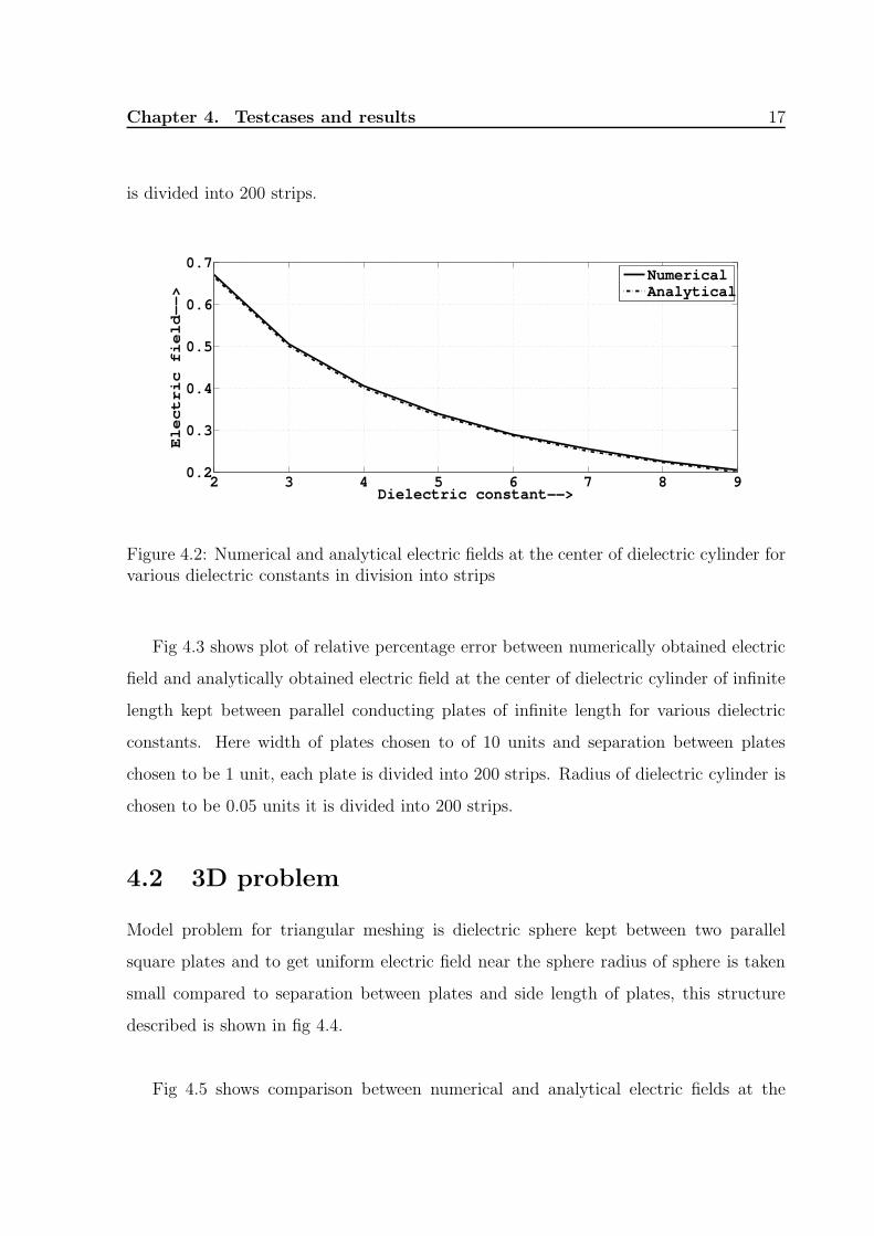
Chapter 4. Testcases and results 17
is divided into 200 strips.
2 3 4 5 6 7 8 90.2
0.3
0.4
0.5
0.6
0.7
Dielectric constant−−>
Ele
ctr
ic f
ield
−−
>
NumericalAnalytical
Figure 4.2: Numerical and analytical electric fields at the center of dielectric cylinder forvarious dielectric constants in division into strips
Fig 4.3 shows plot of relative percentage error between numerically obtained electric
field and analytically obtained electric field at the center of dielectric cylinder of infinite
length kept between parallel conducting plates of infinite length for various dielectric
constants. Here width of plates chosen to of 10 units and separation between plates
chosen to be 1 unit, each plate is divided into 200 strips. Radius of dielectric cylinder is
chosen to be 0.05 units it is divided into 200 strips.
4.2 3D problem
Model problem for triangular meshing is dielectric sphere kept between two parallel
square plates and to get uniform electric field near the sphere radius of sphere is taken
small compared to separation between plates and side length of plates, this structure
described is shown in fig 4.4.
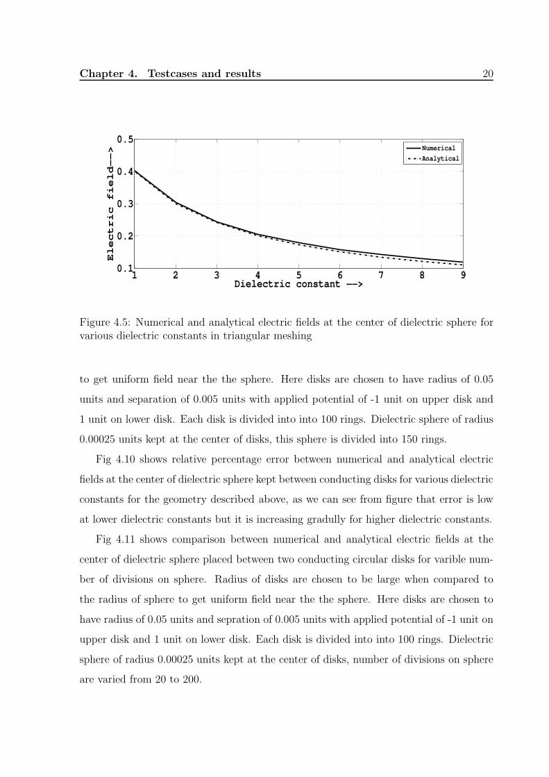
Fig 4.5 shows comparison between numerical and analytical electric fields at the

Chapter 4. Testcases and results 18
2 3 4 5 6 7 8 9−2.5
−2
−1.5
−1
−0.5
Dielectric constant−−>
Re
lative
err
or(
%)−
−>
Figure 4.3: Error between numerical and analytical electric fields at the center of dielec-tric cylinder for various dielectric constants in division into strips
center of dielectric sphere placed between two conducting plates for various dielectric
constants. Here plates chosen are square having side length of 100 units and separation
of 5 units with applied potential of -1 unit on upper plate an 1 unit on lower plate. Each
plate is divided into 30 units along each parameter and points obtained are joined with
triangles. Dielectric sphere of radius 0.25 units kept at the center of plates, this sphere is
divided into 20 units along each parameter and points obtained are joined with triangles.
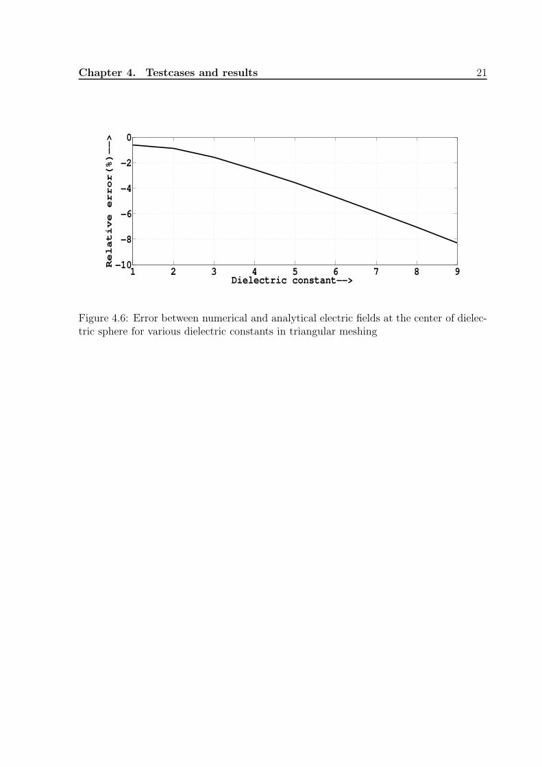
Fig 4.6 shows relative percentage error between numerical and analytical electric
fields at the center of dielectric sphere kept between square plates for various dielectric
constants for the geometry described above, as we can see from figure that error is low
at lower dielectric constants but it is increasing gradully for higher dielectric constants.
Fig 4.7 shows relative percentage error between numerical and analytical electric
fields at the center of dielectric sphere kept between square plates for variable number of
divisions on the dielectric sphere. Here goemetry chosen for plates is square having side
length of 100 units and sepration of 5 units with applied potential of -1 unit on upper
plate an 1 unit on lower plate. Each plate is divided into 30 units along each parameter
Chapter 4. Testcases and results 19
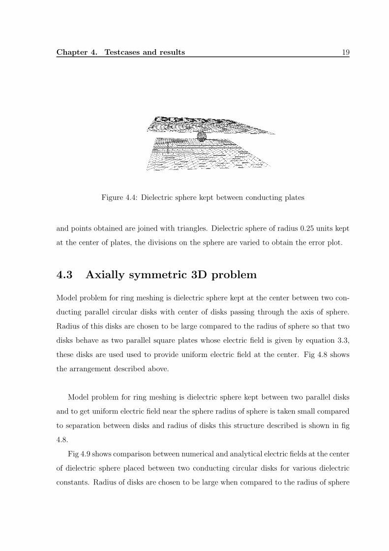
Figure 4.4: Dielectric sphere kept between conducting plates
and points obtained are joined with triangles. Dielectric sphere of radius 0.25 units kept
at the center of plates, the divisions on the sphere are varied to obtain the error plot.
4.3 Axially symmetric 3D problem
Model problem for ring meshing is dielectric sphere kept at the center between two con-
ducting parallel circular disks with center of disks passing through the axis of sphere.
Radius of this disks are chosen to be large compared to the radius of sphere so that two
disks behave as two parallel square plates whose electric field is given by equation 3.3,
these disks are used used to provide uniform electric field at the center. Fig 4.8 shows
the arrangement described above.
Model problem for ring meshing is dielectric sphere kept between two parallel disks
and to get uniform electric field near the sphere radius of sphere is taken small compared
to separation between disks and radius of disks this structure described is shown in fig
4.8.
Fig 4.9 shows comparison between numerical and analytical electric fields at the center
of dielectric sphere placed between two conducting circular disks for various dielectric
constants. Radius of disks are chosen to be large when compared to the radius of sphere
Chapter 4. Testcases and results 20
1 2 3 4 5 6 7 8 90.1
0.2
0.3
0.4
0.5
Dielectric constant −−>
Ele
ctr
ic f
ield
−−
>
Numerical
Analytical
Figure 4.5: Numerical and analytical electric fields at the center of dielectric sphere forvarious dielectric constants in triangular meshing
to get uniform field near the the sphere. Here disks are chosen to have radius of 0.05
units and separation of 0.005 units with applied potential of -1 unit on upper disk and
1 unit on lower disk. Each disk is divided into into 100 rings. Dielectric sphere of radius
0.00025 units kept at the center of disks, this sphere is divided into 150 rings.
Fig 4.10 shows relative percentage error between numerical and analytical electric
fields at the center of dielectric sphere kept between conducting disks for various dielectric
constants for the geometry described above, as we can see from figure that error is low
at lower dielectric constants but it is increasing gradully for higher dielectric constants.
Fig 4.11 shows comparison between numerical and analytical electric fields at the
center of dielectric sphere placed between two conducting circular disks for varible num-
ber of divisions on sphere. Radius of disks are chosen to be large when compared to
the radius of sphere to get uniform field near the the sphere. Here disks are chosen to
have radius of 0.05 units and sepration of 0.005 units with applied potential of -1 unit on
upper disk and 1 unit on lower disk. Each disk is divided into into 100 rings. Dielectric
sphere of radius 0.00025 units kept at the center of disks, number of divisions on sphere
are varied from 20 to 200.
Chapter 4. Testcases and results 21
1 2 3 4 5 6 7 8 9−10
−8
−6
−4
−2
0
Dielectric constant−−>
Re
lative
err
or(
%)−
−>
Figure 4.6: Error between numerical and analytical electric fields at the center of dielec-tric sphere for various dielectric constants in triangular meshing
Chapter 4. Testcases and results 22
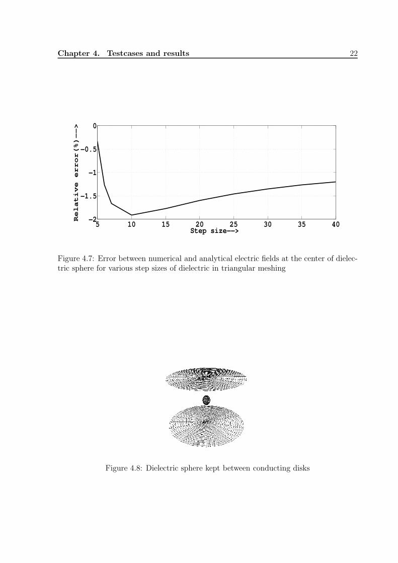
5 10 15 20 25 30 35 40−2
−1.5
−1
−0.5
0
Step size−−>
Re
lative
err
or(
%)−
−>
Figure 4.7: Error between numerical and analytical electric fields at the center of dielec-tric sphere for various step sizes of dielectric in triangular meshing
Figure 4.8: Dielectric sphere kept between conducting disks

Chapter 4. Testcases and results 23
1 2 3 4 5 6 7 8 9100
200
300
400
500
Dielectric constant−−>
Ele
ctr
ic fie
ld−
−>
NumericalAnalytical
Figure 4.9: Numerical and analytical electric field at the center of dielectric sphere forvarious dielectric constants in ring meshing
1 2 3 4 5 6 7 8 9−8
−6
−4
−2
0
Dielectric constant−−>
Re
lative
err
or(
%)−
−>
Figure 4.10: Error between numerical and analytical electric field at the center of dielec-tric sphere for various dielectric constants in ring meshing
Chapter 4. Testcases and results 24
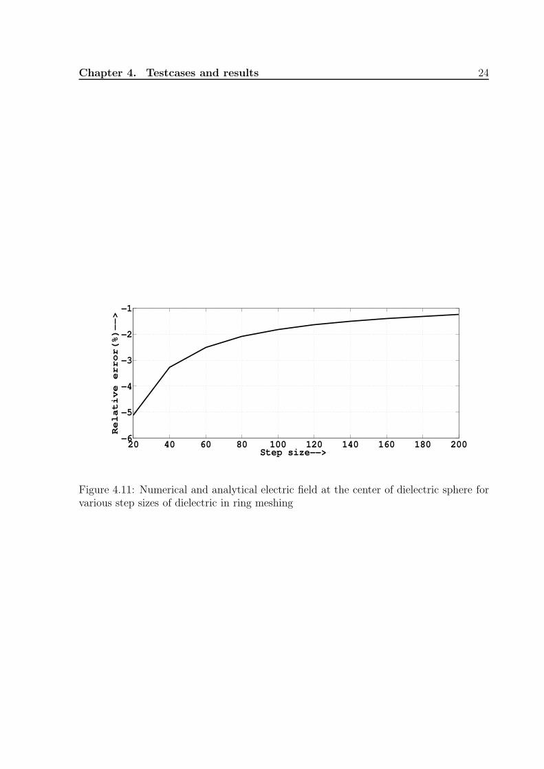
20 40 60 80 100 120 140 160 180 200−6
−5
−4
−3
−2
−1
Step size−−>
Re
lative
err
or(
%)−
−>
Figure 4.11: Numerical and analytical electric field at the center of dielectric sphere forvarious step sizes of dielectric in ring meshing
Chapter 5
Conclusions and Future work
5.1 Conclusions
Ring meshing is observed to give less error when compared to triangular meshing, size of
matrix obtained in case of ring meshing is very less when compared to triangular meshing
so computation time is very less using ring meshing, but ring meshing can be applied to
only axially symmetric objects, so in case of axially symmetric objects ring meshing is
efficient and triangular meshing is useful in case of any 3D objects.
5.2 Future work
Implementation of code to handle floating electrodes can be included, efficient imple-
mentation of obtaining potential and electric field at any point in case of perturbation
in the boundary of electrodes, obtaining capacitance if certain electrodes potential and
boundaries are given.
25
References
[1] D. J. Griffiths, Introduction to Electrodynamics, Prentice-Hall inc 1999, Third Edi-
tion.
[2] E. Kreyszig, Avanced Engineering Mathematics, John Wiley Sons inc 1999, Eighth
Edition.
[3] W. H. Arfken G.B, Mathematical Methods For Physicists, 2005.
[4] O.D.Kellog, Foundations in potential theory, Frederick Ungar Publishing Company,
1929.
[5] W. R.Smythe, Static and Dynamic Electricity, McGraw-Hill Book Company, July
1950, Second Edition.
[6] E. Weber, Electromagnetic Fields: Theory and Applications, New York: John Wiley
Sons, 1950.
[7] C. Brebbia and J. Dominguez, Boundary Elements An Introductory Course, 1998.
[8] P. K. Banerjee, The Boundary Element Methods in Engineering, McGraw-Hill Book
Company, 1994.
[9] A. Krishnaveni, R. Neeraj Kumar Verma, A. G. Menon, and A. K. Mohanty, Numer-
ical observation of preferred directionality in ion ejection from stretched rectilinear
ion traps, International Journal of Mass Spectrometry, vol. 275, pp. 1120, 2008.
26

REFERENCES 27
[10] P. Tallapragada, A. K. Mohanty, A. Chatterjee, and A. G. Menon, Geometry opti-
mization of axially symmetric ion traps, International Journal of Mass Spectrometry,
vol. 264, pp. 3852, 2007.
Recommended