1
Huntsville, AL Chapter
Electrostatic Discharge –
The Phenomena, Design Guidance and
Testing for Improving Product Immunity
Huntsville, Alabama
January 15, 2009
Huntsville, AL Chapter
The ESD Phenomena
Causes, Characteristics and Effects
Design Guidance
Equipment Construction and PCB Layout
Testing Considerations
Processes, Facilities and Equipment
Summary - Q & A
Agenda

2
Huntsville, AL Chapter
Electromagnetic Interference Model
Source
Path Victim
Phenomena
Huntsville, AL Chapter
Why concern ourselves with Electrostatic Discharge in the first
place?
Effects range from Nuisance to Catastrophic
Reliability and Time to Market
Electromagnetically Compatible Environment
Phenomena

3
Huntsville, AL ChapterPhenomena
Huntsville, AL Chapter
Electrostatic Discharge is described as the abrupt release of
static charge from one object to another.
When materials are brought into contact with one another and
separated one material will release charge (electrons) while the
other will accept this charge.
The tendency to accept or release charge is dependant on
many factors – including type of material, method and duration
of contact.
Once a charged surface is brought into proximity or contact with
another surface that is of lower resistance to ground a sudden
and intense transfer of energy will occur.
Phenomena

4
Huntsville, AL Chapter
Typical Triboelectric Series
POSITIVE
1. Air
2. Human Skin
3. Asbestos
4. Glass
5. Mica
6. Human Hair
7. Nylon
8. Wool
9. Fur
10. Lead
11. Silk
12. Aluminum
13. Paper
14. Cotton
15. Wood
16. Steel
17. Sealing Wax
18. Hard Rubber
19. Mylar
20. Epoxy Glass
21. Nickel, Copper
22. Brass, Silver
23. Gold, Platinum
24. Polystyrene Foam
25. Acrylic
26. Polyester
27. Celluloid
28. Orlon
29. Polyurethane Foam
30. Polyethylene
31. Polypropylene
32. PVC (vinyl)
33. Silicon
34. Teflon
NEGATIVE
Phenomena
Huntsville, AL Chapter
Fast rise time, intense
peak with relatively
short duration.
Can be many amps of
current with very high
voltages
Typical ESD Voltage Levels
Means of Generation10-25%
RH
65-90%
RH
Walking across carpet 35,000V 1,500V
Walking across vinyl tile 12,000V 250V
Worker at bench 6,000V 100V
Poly bag picked up from bench 20,000V 1,200V
Chair with urethane foam 18,000V 1,500V
Phenomena

5
Huntsville, AL Chapter
Effects of ESD –
Conduction – Currents flowing through circuitry causing
breakdown and failure.
Secondary Arcing – Currents flowing through circuitry as a
result of proximity to initial arc
Capacitive and Inductive coupling (E/H-Field) – Fields are
produced as a result of current flowing through discharge
path; these fields induce voltage and currents into adjacent
circuitry through coupling
Phenomena
Huntsville, AL Chapter
Conduction and Secondary Arcing–
Assumptions:
10nH/cm of inductance on circuit trace
1 cm trace
10A of current in 1ns of time
Leads to 100V/cm of voltage along the trace
V=L dI/dT
5pf of capacitance from signal trace to return path (ground)
1000 V charge in 1 ns
Leads to 5A of current injected on the signal
I = C dV/dT
Phenomena

6
Huntsville, AL Chapter
Fields Example –
Phenomena
Huntsville, AL Chapter
Capacitive and Inductive Coupling –
Introduction of a 2kV ESD event into a test fixture resonant
cavity
Differential mode Common mode
Phenomena

7
Huntsville, AL Chapter
Effects on Hardware –
Performance
Data errors, loss of stored data
Loss of Sync
Change of state
Reset, loss of power
Damage
Phenomena
Huntsville, AL Chapter
Approach for EMI resolution –
Logical, systematic and consistent evaluation
Prevent the occurrence of the ESD Event
Removal or reduction of the coupling path
Increasing the inherent immunity of the product
Source
Path Victim
Design

8
Huntsville, AL Chapter
Prevent Occurrence – Control Products and Handling
Design
Huntsville, AL Chapter
33% of the problem solved, right? – So now what …?
Removal or reduction of the coupling path
Increasing the inherent Immunity of the product
Mechanical/Construction
PCB layout
Component Selection and placement
Testing Considerations
Design

9
Huntsville, AL Chapter
General –
Susceptibility to an ESD event can have a variety of
sources not always related to the product
Start with the big picture and narrow the search
Examine the nature of the failure for indicators of the
source
Changes that exist from one product to another – new
products, product revisions or devices
Strive for repeatable processes to reduce ‘false’ failures
A proper grounding scheme is the basic tool for ESD
Immunity
Design
Huntsville, AL Chapter
Mechanical/Construction issues –
Planned, Low impedance path - Route away from sensitive
circuitry or cabling as much as possible – use distance to your
advantage
Wider is better – High Frequency energy takes the path of least
inductance - on the outer portion of the conductor (skin effect).
Increasing the available surface area will improve the path
performance
Dependable Ground connections – Clips, Mounting holes, stand-
offs and long support tabs
Plastic housings or lack of Earth Ground connections require
special consideration
Design

10
Huntsville, AL Chapter
Mechanical/Construction issues –
Masking of painted mating surfaces including mounting tabs and
screw holes (DB9 connectors) –allow for maximum misalignment
in assembly
Protect Displays (LCD/LED) or other with Mylar film or with
distance – recess displays.
Use of Light pipes or other non-conductive materials may be used
to provide isolation of potentially sensitive circuitry
This may have some advantages in material costs both in the
construction material and less parts required for filtering
Protect other components near the faceplate or surfaces where
charge may be present – switches, reset buttons etc…use of filter
components
Design
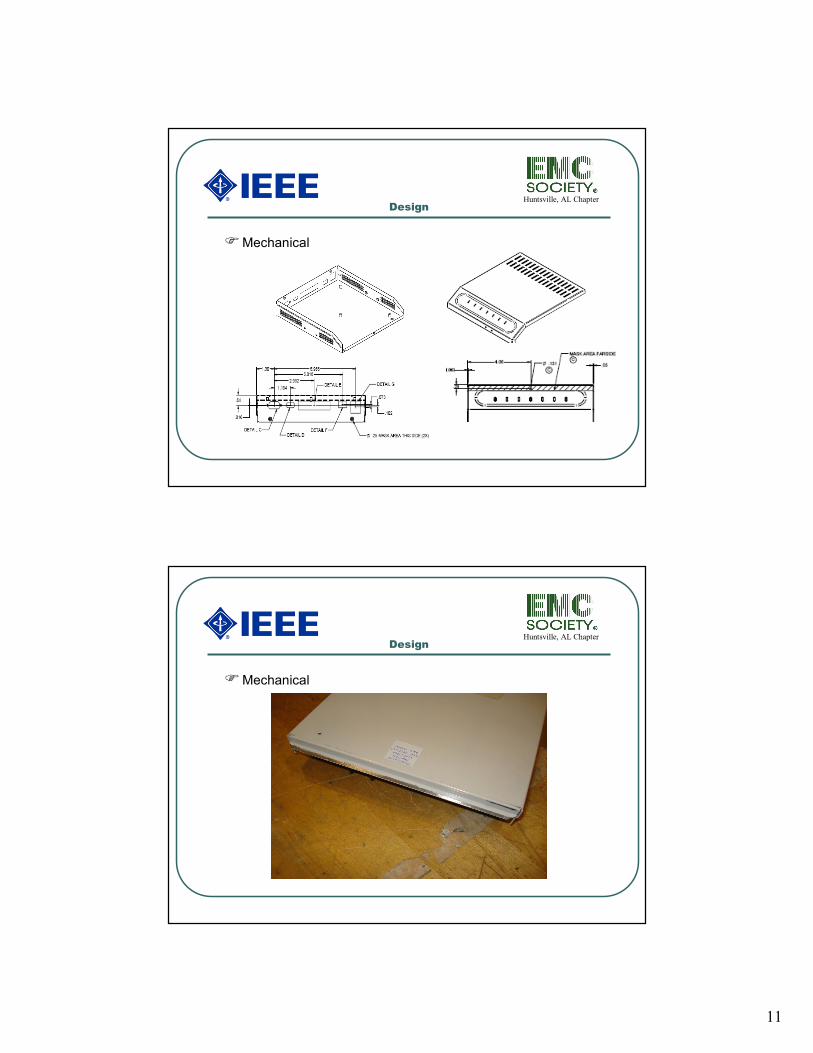
Huntsville, AL Chapter
Mechanical
Design
11
Huntsville, AL Chapter
Mechanical
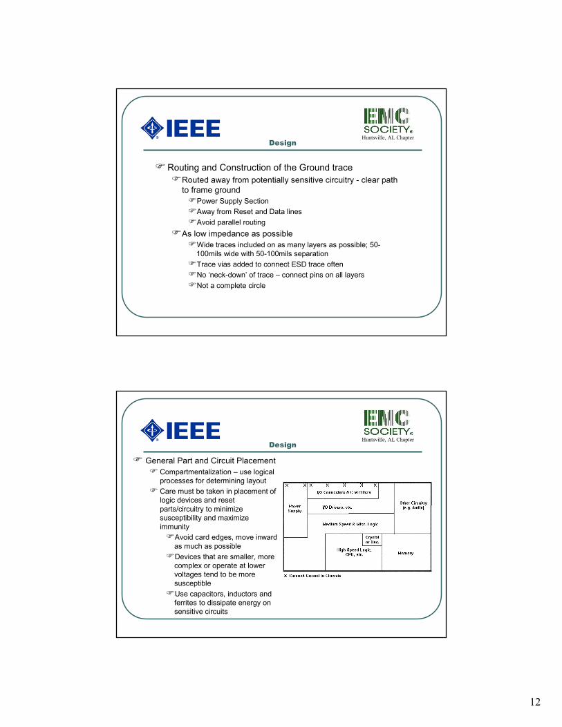
Design
Huntsville, AL Chapter
Mechanical
Design
12
Huntsville, AL Chapter
Routing and Construction of the Ground trace
Routed away from potentially sensitive circuitry - clear path
to frame ground
Power Supply Section
Away from Reset and Data lines
Avoid parallel routing
As low impedance as possible
Wide traces included on as many layers as possible; 50-
100mils wide with 50-100mils separation
Trace vias added to connect ESD trace often
No ‘neck-down’ of trace – connect pins on all layers
Not a complete circle
Design
Huntsville, AL Chapter
General Part and Circuit Placement
Compartmentalization – use logical
processes for determining layout
Care must be taken in placement of
logic devices and reset
parts/circuitry to minimize
susceptibility and maximize
immunity
Avoid card edges, move inward
as much as possible
Devices that are smaller, more
complex or operate at lower
voltages tend to be more
susceptible
Use capacitors, inductors and
ferrites to dissipate energy on
sensitive circuits
Design

13
Huntsville, AL Chapter
– Discharge path routing/clearance
Design
Huntsville, AL Chapter
Reset Circuitry
Use simple routing
Close to logic inputs
Use short traces, route with 1st priority after clock lines or
other critical nets
Away from faceplates, board edges and static discharge path
- avoid parallel routing
Avoid crossing moats in planes – large voltage swings can
occur during ESD events
Operate off the highest voltage possible – lower voltage
circuits tend to be more sensitive to ESD
Use capacitors (typically .1uf) on each reset line ferrites
may be used in addition for particularly sensitive parts.
Design

14
Huntsville, AL Chapter
– Reset Circuitry
Design
Huntsville, AL Chapter
Critical nets and Debug Circuitry
Avoid routing critical traces parallel to Frame Ground
(Discharge path)
Faceplates, chassis surfaces are part of Frame Ground
Proper spacing
Use 90 degree angle for placement
Debug Circuitry/Header connectors
Great for development – can be painful in testing
Mind part placement rules for location of Debug headers
Remove debug headers from test samples – energy can
couple to leads
Use no load 0 ohm resistors at sources to eliminate
stubs on board – keep in mind for other nets; test points
etc…
Design

15
Huntsville, AL Chapter
Clock/Critical Net routing
Design
Huntsville, AL Chapter
- Debug Header
Design

16
Huntsville, AL Chapter
Ground and Power Planes
Digital Ground planes and Power planes may serve as shields or
insulators from ESD
More Power and Ground fill available results in lower overall
inductance – voltages developed by ESD will be lower and more
easily dissipated – wider is still better
Taking advantage of imbedded capacitance by having well
coupled Power and Ground planes will not only improve high
frequency emissions - overall ESD performance should be
improved. A great deal of High Frequency energy is produced in
an ESD event
Planes should be recessed as much as possible from potentially
charged surfaces, mounting holes, connections or intended
discharge path
Design
Huntsville, AL Chapter
– Plane Clearance
Design

17
Huntsville, AL Chapter
IEC EN 61000-4-2
Describes testing and measurement techniques for
Commercial Electrostatic Discharge Immunity Tests
Defines a variety of parameters including:
Test Equipment
Physical arrangement of Equipment Under Test, Support
Equipment and cabling
Laboratory conditions for testing
Conduct of the test
Testing
Huntsville, AL Chapter
Test Equipment –
Variety of shapes,
sizes and
manufacturers
Intended to simulate
the Human Body
Model (and others)
Most commonly
150pf/330Ω +10%
Require calibration and
proper use
Testing

18
Huntsville, AL Chapter
Comparison of 61000-4-2 waveform to measured
waveform
Testing
Huntsville, AL Chapter
ESD testing is easily affected by outside influences –
Tolerances associated with test equipment
Test setup anomalies including:
Improper bonding/test arrangement
Improper application of Discharges
Temperature and Humidity
Testing

19
Huntsville, AL Chapter
Things Mama didn’t tell
us -
Table-top testing
Bleed resistors
Insulating Material
Coupling of cables to
table top
Testing
Huntsville, AL ChapterTesting
More things Mama didn’t
tell us -
Floor-standing testing
Arrangement of
Generator return cable
EUT cable arrangement
Don’t hold the VCP with
your hand!

20
Huntsville, AL Chapter
Approach for Debug – Who Me?
Setup issues associated with the Equipment under
Test and Associated Support Equipment (Could be
the Test Lab – I’m off the hook)
Setup issues associated the test generation side of
things including Climatic conditions (those Lab guys
again)
OK – I guess it’s the product
Since we’ve already followed all the rules what next?
Testing
Huntsville, AL Chapter
Since we’re looking at the product now – start painting
with a wide brush
Evaluate for deviations from the design guidelines – verify
and mitigate if possible
Consider Software/Functionality issues
Examine the characteristics of the problem
Isolate Operationally – software/hardware/other
Isolate Physically
Probe position – discharge application
Near field probing using decreasing levels
Once sensitive circuits are located, treat accordingly
Leave Rube Goldberg modifications in place until the problem
is solved then back out changes individually for effect
Testing

21
Huntsville, AL Chapter
Summary –
Begin with sound design and installation practices
If you’re still in trouble the use of a logical, systematic
and consistent evaluation of all of the possible
contributing factors will eventually drill down to the
root cause
Given the characteristics of the problem, start with a
wide perspective
Don’t give up -
???
Summary – Q & A
Huntsville, AL Chapter
Noise Reduction Techniques In Electronic Systems
2nd Edition, 1998. By Henry W. Ott
Introduction to Electromagnetic Compatibility, 2nd Edition, 2006. By Clayton R.
Paul
Engineering Electromagnetic Compatibility, 2nd Edition, 2001. By V. Prasad
Kodali
IEC 61000-4-2 Ed 1.1, 1995-05 Electromagnetic Compatibility (EMC) – Part 4-2:
Testing and Measurement Techniques – Electrostatic discharge immunity test
“Modeling of Electromagnetic Interference Induced by Electrostatic Discharge
(ESD) Inside Resonant Structures” Graziano Cerri, Member, IEEE, Roberto De
Leo, Valter Mariani Primiani, Member, IEEE, and Stefano Pennesi
http://www.dsmith.org
http://www.esda.org/
References
Recommended