URRENT
ENSORSCS
ELECTRONICS COMPONENTS

Content
Group network map ・・・・・・・・・・・・・・・・・・・・・・・・・ 1
Outline / Applications / Features / Applications map / Guide map ・・・・・・・・・・・・・・・・・・・・・・・・・ 2
Circuit system / Application notes / Part numbering system / Methods of electrical characterization and measurement
・・・・・・・・・・・・・・・・・・・・・・・・・ 6
Important Notice ・・・・・・・・・・・・・・・・・・・・・・・・・ 9
According to UL508 standard and CSA C22.2 No.14 standard ・・・・・・・・・・・・・・・・・・・・・・・・・ 10
Data sheetF-Series, L-Series, S-Series ・・・・・・・・・・・・・・・・・・・・・・・・・ 15
CURRENT SENSORS Content 1/1 2 1602

●■▲Tamura Europe Limited (U.K.)●Tamura Kaken (U.K.) Ltd. ●▲Tamura Corporation
of America
●■▲Tamura Electronics(Malaysia) SDN.BHD.
●■▲Tamura Chemical Korea Co.,Ltd.
●■●●Tamura Corporation of Korea
■▲Tamura Electronics(Shenzhen) Co.,Ltd.
●▲Tamura Power Technology Co., Ltd.
●■▲ Shanghai Xiangle Tamura Electro Chemical Industry Co., Ltd.
●Tamura Kaken(Malaysia) SDN.BHD.
●Tamura Kaken Corp.,U.S.A.
●Telepart-Tamura Industria E ComercioLTDA.
■ Tamura Seiko Electronics(Changshu) Co., Ltd.
■●Tamura Europe LimitedCzech branch
■Tamura Power Technologies de Mexico, S.A., DE C.V.
●●Tamura Corporation (Thailand)Co., Ltd.
●■▲Tamura FA System (Suzhou) Corporation
■Op-Seed Co.,(BD)Ltd.
●Tamura Kaken Tech Co., Ltd.
●■Tamura Kaken(Dongguan) Ltd.
■Tamura ElcomponicsTechnologies Pvt. Ltd.
●● Tamura Corporation Singapore Pte. Ltd.
■▲ Tamura Electronics(Huizhou) Co.,Ltd.
●● Tamura Corporation of Hong Kong Limited
Group Network - Overseas ○: Sales □: Factory △: R&D
●▲● Tamura Corporation ofChina Limited
●:Electronic components●:Electronic chemicals / FA systems ●:Information Equipment ●:General and administrative
●■ Tamura Electronic Material(Tianjin)Co.,Ltd.
■ Hefei Ecriee-Tamura ElectricCo., Ltd.
■ Industria Sul Brazil de Transformadores Ltda.
■ Indusul Industria deTransformadores Ltda.
●Tamura Corporation VietnamCo., Ltd.
Factory and R&D for Current sensor
Group Network - Japan ○: Sales □: Factory △: R&D
●■▲ Tamura CorporationSakado factory
● Tamura CorporationKodama factory
●■▲ Tamura CorporationSayama factory
● Tamura Distribution Center Inc.
■■ Aizu Tamura Corporation ■ Wakayanagi Tamura Corporation
●:Electronic components●:Electronic chemicals / FA systems ●:Information Equipment ●:General and administrative
●●Nagoya sales office
Tamura Corporation● head office/●▲Tokyo factory
▲Tamura CorporationCore-technology center
●●●Osaka sales office
●■▲ Tamura CorporationIruma factory
●■▲ Koha Co., Ltd.
■ Anzen Dengu (Huizhou)Co., Ltd.
Group network map
CURRENT SENSORS Group 1/1 3 1704
Intr
oduc
tion
Flux
gate
sys
tem
O
pen
loop
Cl
osed
loop
1

Outline / Applications / Features
The current sensor is a sensor to measure the current as its name. However, The current is various. There is a current value up to 10k amperes treated in the power plant from 1mA, and the shape of current waves also has AC, DC, and AC + DC. Since a method and a structure the best in each measuring object are different, there are also various current sensors. Tamura supplies the sensor using the Hall-Effect system for measuring the current value from several amperes to several kilo-ampere.
The Hall-Effect current sensor measures the magnetic flux produced in proportion to the primary current without any direct contact with the primary circuit; the combination of the Hall element and magnetic circuit provide excellent solution for measuring AC/ DC current with galvanic isolation and zero insertion loss.The diagram in Figure-1 depicts the Hall current sensor basic principle. The magnetic flux produced in proportion to the primary current, If, induced in the magnetic circuit, passes through the Hall element inserted in the gap of the magnetic circuit resulting in a potential difference, Vh, expressed by the following formula:
Current control and detection of over-current in various types of inverters. Used for general-purpose inverter, various types of power conversion equipment to control and to detect over-current. Also used to measure DC current from the battery.● Various types of inverters (CVCF, vector), Industrial robots,
automation, devices, NC● UPS, Elevator, Laser Cutting Machines, Welding Machines, Various
types of Regulated Power Supply● Solar power generation systems, Wind power systems, Fuel cell
systems
Measurement of DC, AC (kHz range), & complex current (AC+DC). Our current range is 3A to 1500A in various mechanical configurations.● Galvanic isolation with many UL compliant configurations.● Fast response time● High Reliability
Figure-1
Vh = k · Ic · B ····· (1)◦Vh ・・・・・・ Hall voltage
◦K ・・・・・・・ Coefficient of sensibility
◦Ic ・・・・・・・ Control current
◦B ・・・・・・・ Magnetic fluxdensity
The induced Vh is small and is amplified by an amplification circuit.
Outlines
Applications Features
CURRENT SENSORS Outlines 1/1 4 1405
Intr
oduc
tion
Flux
gate
sys
tem
O
pen
loop
Cl
osed
loop
2
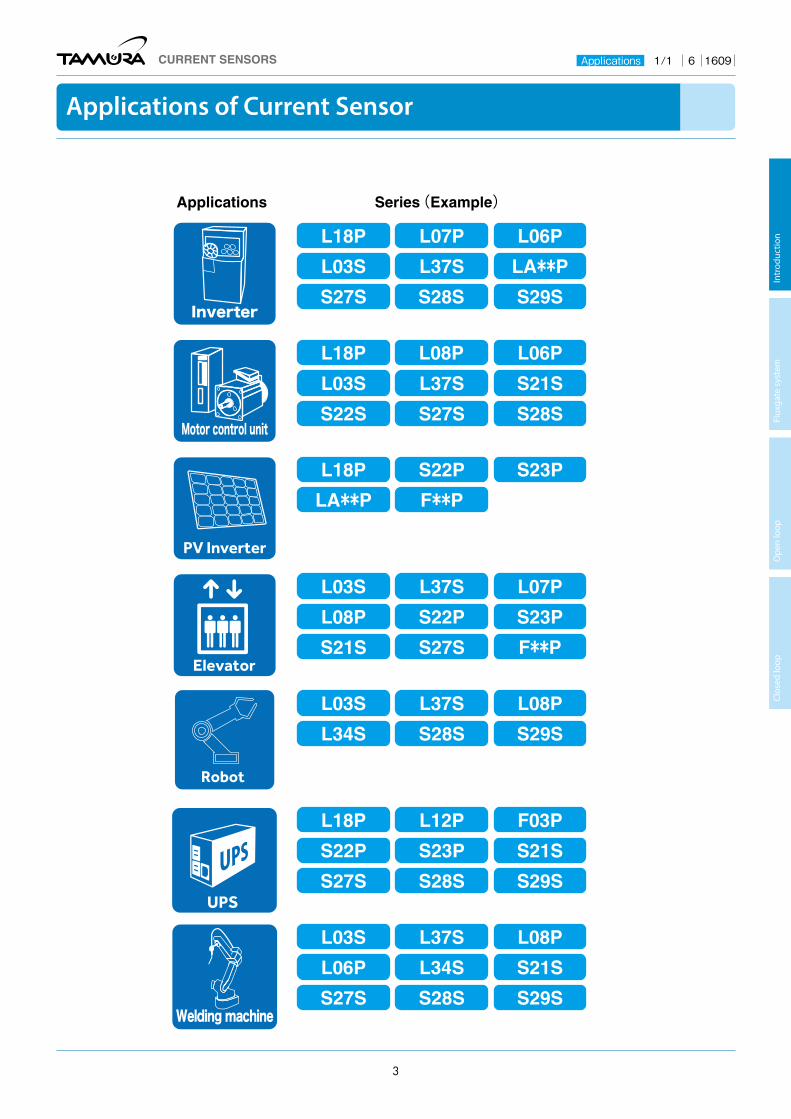
Applications of Current Sensor
Applications Series (Example)
L06P
L37S LA**PL03S
L07PL18P
S28S S29SS27S
S21SL03S L37S
L08P L06PL18P
S28SS22S S27S
S23PL18P S22P
LA**P F**P
L07PL03S L37S
S23PL08P S22P
F**PS21S S27S
L08PL03S L37S
S29SL34S S28S
F03PL18P L12P
S21SS22P S23P
S29SS27S S28S
L08PL03S L37S
S21SL06P L34S
S29SS27S S28SWelding machine
CURRENT SENSORS Applications 1/1 6 1609
Intr
oduc
tion
Flux
gate
sys
tem
O
pen
loop
Cl
osed
loop
3

Current Sensor / Guide map
SERIES Model
Main Specification UL
R/C
Features PageCircuit System
MountingConfiguration
PrimaryConductor
RatedCurrent
PowerVoltage
F01PF01PxxxS05L F01PxxxS05
Fluxgate system On-board Built-in
bus-bar 6~50A +5V ●
• Super precision &High stability• F02P & F03P:With reference
access• F03P:Longer creepage and
clearance distances• Name end“L”;Backward
compatible, Anti-Surge current, Compact
15
F02PF02PxxxS05L F02PxxxS05
F03PF03PxxxS05L F03PxxxS05
F23PF23PxxxS05R
Fluxgate system On-board Built-in
bus-bar 50-100A +5V ● ・Super precision & High stability・With reference access 51
L18P L18PxxxD15-OPSL18PxxxD15L18PxxxD15
Open loop On-boardBuilt-in coil/
bus-bar3~60A
±15V
●
• Low cost • Compact, high performance • Name First “SL18P”; Anti-Sulfurated
(Coating, Anti-Sulfurated re-sistance)• Name end “R”; Rated voltage change
57L18PxxxS05L18PxxxS05R
+5V
L18PxxxS12 +12V
L07P L07PxxxD15
Open loop On-board Built-incoil 3~30A
±15V●
• Low cost • Built-in 2 circuits • Name end “S”;Anti-Sulfurated
(Coating, Anti-Sulfurated resistance)
63L07PxxxD15S
L07PxxxS05 +5V
L12PL12P025D15 Open loop On-board Built-in
coil 25A ±15V • Low cost• Compact 66
L32P L32PxxxS05BFS
Open loop On-board
Built-in bus-bar 50A, 100A
+5V ●• Ferrite core is used.• With reference access• Used Anti-Sulfurated resistance
67L32PxxxS05FS
Through hole□15×8 50~400A
L08P L08PxxxD15
Open loop On-board Through holeφ16
5~200A
±15V• Wide range of applications• Name end“W”;Saturation current up, NC pin is deleted.
68L08PxxxD15W/IPV
50~500A
L01ZL01ZxxxS05 Open loop On-board Through hole
□15×8 50~600A +5V • Wide electrical current range• Compact 71
L37S L37SxxxD15M L37SxxxD15J
Open loop Connector(MOLEX/JST)
Through hole□20.4×10.4 50~600A ±15V ●
• Design for lower dvdt noise• Succession model of L03SxxxD15W
series• Wide electrical current range• Compact
72
L03S L03SxxxD15
Open loop
Connector(MOLEX) Through hole
□20.5×10.5
50~600A±15V
• Wide electrical current range• Compact• Name end"W"; Saturation current up,
Change position of CN (MOLEX or JST)
75L03SxxxD15WML03SxxxD15WJ
Connector(MOLEX/JST) 50~800A
L31SL31SxxxS05FS Open loop Connector
(MOLEX)Through hole□20.5×10.5 50~600A +5V ●
• Wide electrical current range• Ferrite core is used.• With reference access• Used Anti-Sulfurated resistance
77
L06P L06PxxxS05 Open loop On-board Through hole
φ22 300~800A +5V • Wide range of applications• Single power supply type 78
NEW
NEW
CURRENT SENSORS Guide Map 1/2 12 1704
Intr
oduc
tion
Flux
gate
sys
tem
O
pen
loop
Cl
osed
loop
4

SERIES Model
Main Specification UL
R/C
Features PageCircuit System
MountingConfiguration
PrimaryConductor
RatedCurrent
PowerVoltage
L05ZL05Z800S15 Open loop Connector
(JST)
Through hole□20.5×
10.5800A +15V • Wide range of applications
• Single power supply type 79
L34SL34SxxxD15 Open loop Connector
(MOLEX)
Through hole□40.5×
40.5200~1500A ±15V ●
• High-Curent (1500A_max) • Wide electrical current range• Large aperture
80
LA01P(M) LA04P LA01MxxxS05
Open loop
On-board(SMT)
Built-inbus-bar
21~41A*1
+5V
• Open loop - one chip ASIC model• Low profile package(8.5mm on PCB)• High-speed response*1:Measurement current range
81LA01PxxxS05
On-board(Discrete)
35~85A*1
LA04P170S05170A
*1
LA02PLA03P LA02PxxxS03
Open loop On-board(Discrete)
Built-inbus-bar
21~85A*1
+3.3V
●
• Open loop - one chip ASIC model• Creepage distance:13mm• Low profile package(9.2mm on PCB)• High-speed response*1:Measurement current range
96
LA03PxxxS05 +5V
S22P
S22PxxxS05M2S22PxxxS05P
Closed loop On-board Built-in bus-bar 6~25A +5V ●
• Voltage - output type • Name end”M2”; Backward compatible
of normal model, External magnetic field improvement model
• Name end “P”; Short lead model of normal model
106
S23P
S23PxxxD15M2S23PxxxD15M1S23PxxxD15
Closed loop On-board Built-in bus-bar 100A ±15V ●
• High accuracy, High performance• Name end"M2"; Backward compatible,
dv/dt improvement type• Name end"M1": Conversion Ration
1:1000• Conversion Ration - Normal & M2
type are 1:2000
108
S25P S25P050D15XS25P100D15YS25P100D15XS25P150D15Y
Closed loop On-board Through hole□13×8.5 50~150A ±15V ●
• High accuracy, High performance • Conversion Ration 1:1000 (Name
end “X”), 1:2000 (Name end “Y”)111
S21S S21S180D15JN Closed loop Connector
(JST)Through hole
R10 180A ±15V ● • Semicircle aperture• Conversion Ration 1:4000 112
S20SS20S200D15M1 Closed loop Connector
(JST)Through hole
φ20.5 200A ±15V • High accuracy, High performance• Conversion Ration 1:2000 113
S26PS26P200D15Y Closed loop On-board Through hole
□17×11 200A ±15V ● • High accuracy, High performance• Conversion Ration 1:2000 114
S27SS27S300D15YS27S300D15YM
Closed loop Connector(MOLEX)
Through holeφ20 300A ±20V ●
• High accuracy, High performance • Conversion Ration 1:2000 • Connector:MOLEX (2 type)
115
S28SS28S500D24ZS28S500D24ZM
Closed loop Connector(MOLEX)
Through holeφ30 500A ±24V ●
• High-current, High accuracy • Conversion Ration 1:5000 • Connector:MOLEX (2 type)
117
S29SS29S1T0D24ZS29S1T0D24ZMS29S1T0D24ZJ
Closed loop Connector(MOLEX/JST)
Through holeφ38.5 1000A ±24V ●
• High-current, High accuracy • Conversion Ration 1:5000 • Connector:MOLEX (2 type), JST (1 type)
119
CURRENT SENSORS Guide Map 5/2 12 1612
Current Sensor / Guide map
Guide Map 2/2 12 1704
Intr
oduc
tion
Flux
gate
sys
tem
O
pen
loop
Cl
osed
loop
5
Circuit system
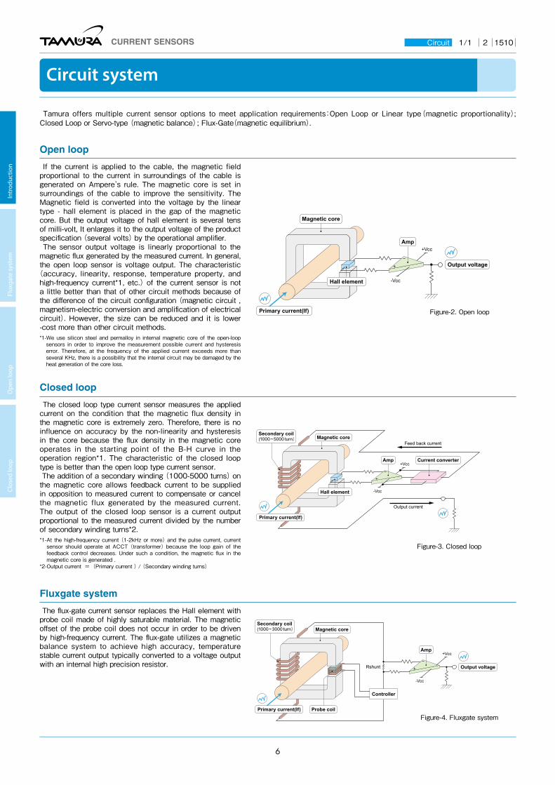
Tamura offers multiple current sensor options to meet application requirements:Open Loop or Linear type(magnetic proportionality); Closed Loop or Servo-type (magnetic balance); Flux-Gate(magnetic equilibrium).
Open loop
If the current is applied to the cable, the magnetic field proportional to the current in surroundings of the cable is generated on Ampere's rule. The magnetic core is set in surroundings of the cable to improve the sensitivity. The Magnetic field is converted into the voltage by the linear type - hall element is placed in the gap of the magnetic core. But the output voltage of hall element is several tens of milli-volt, It enlarges it to the output voltage of the product specification (several volts) by the operational amplifier. The sensor output voltage is linearly proportional to the magnetic flux generated by the measured current. In general, the open loop sensor is voltage output. The characteristic
(accuracy, linearity, response, temperature property, and high-frequency current*1, etc.) of the current sensor is not a little better than that of other circuit methods because of the difference of the circuit configuration (magnetic circuit , magnetism-electric conversion and amplification of electrical circuit). However, the size can be reduced and it is lower -cost more than other circuit methods.*1- We use silicon steel and permalloy in internal magnetic core of the open-loop
sensors in order to improve the measurement possible current and hysteresis error. Therefore, at the frequency of the applied current exceeds more than several KHz, there is a possibility that the internal circuit may be damaged by the heat generation of the core loss.
Figure-2. Open loop
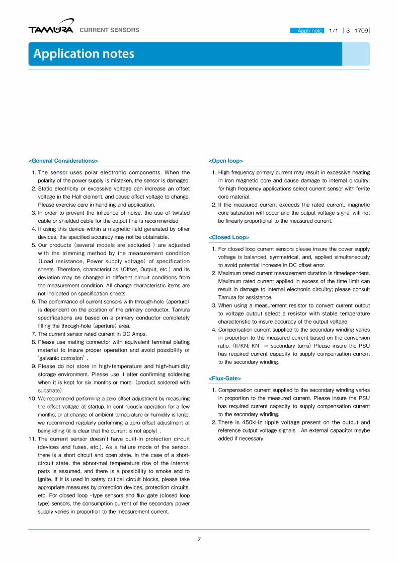
Closed loop
The closed loop type current sensor measures the applied current on the condition that the magnetic flux density in the magnetic core is extremely zero. Therefore, there is no influence on accuracy by the non-linearity and hysteresis in the core because the flux density in the magnetic core operates in the starting point of the B-H curve in the operation region*1. The characteristic of the closed loop type is better than the open loop type current sensor. The addition of a secondary winding (1000-5000 turns) on the magnetic core allows feedback current to be supplied in opposition to measured current to compensate or cancel the magnetic flux generated by the measured current. The output of the closed loop sensor is a current output proportional to the measured current divided by the number of secondary winding turns*2. *1- At the high-frequency current (1-2kHz or more) and the pulse current, current
sensor should operate at ACCT (transformer) because the loop gain of the feedback control decreases. Under such a condition, the magnetic flux in the magnetic core is generated .
*2-Output current = (Primary current ) / (Secondary winding turns)
Figure-3. Closed loop
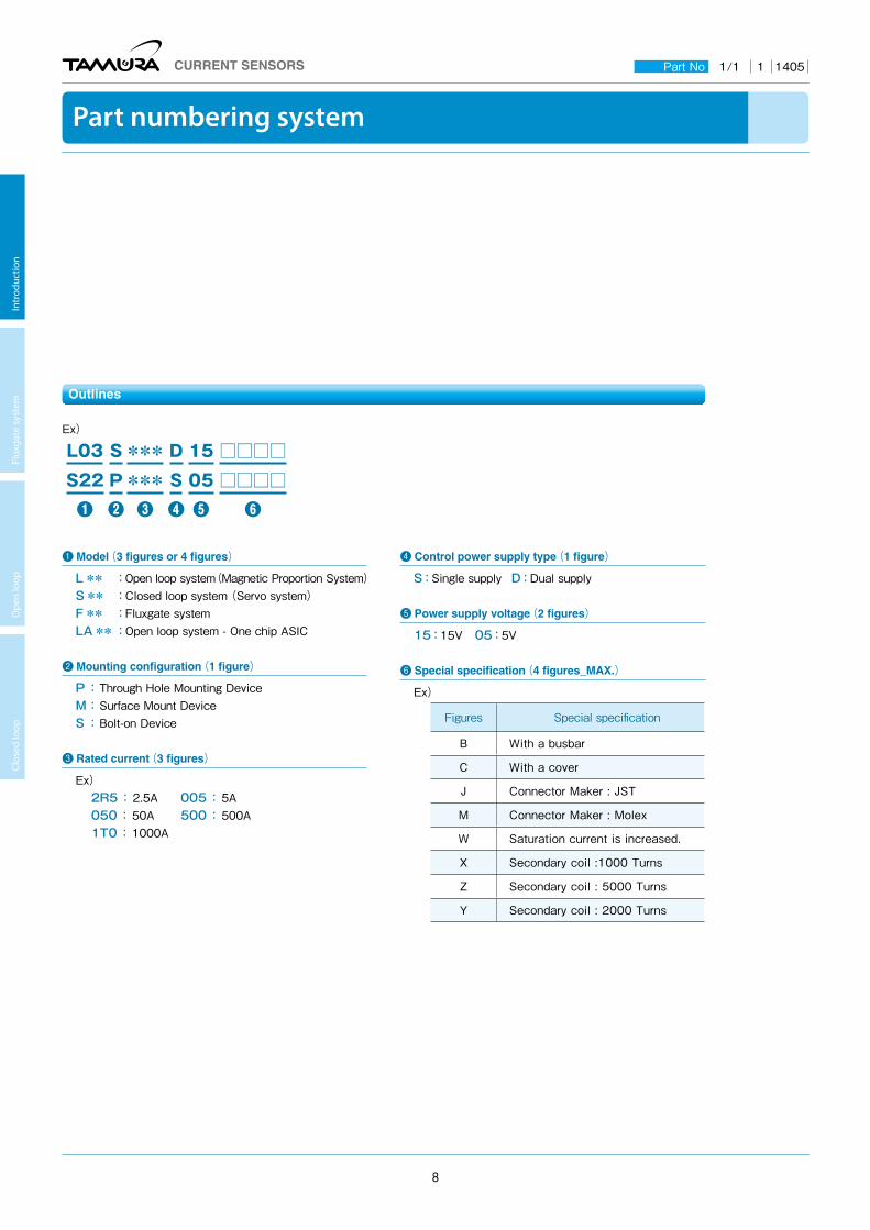
Fluxgate system
The flux-gate current sensor replaces the Hall element with probe coil made of highly saturable material. The magnetic offset of the probe coil does not occur in order to be driven by high-frequency current. The flux-gate utilizes a magnetic balance system to achieve high accuracy, temperature stable current output typically converted to a voltage output with an internal high precision resistor.
Figure-4. Fluxgate system
CURRENT SENSORS Circuit 1/1 2 1510
Intr
oduc
tion
Flux
gate
sys
tem
O
pen
loop
Cl
osed
loop
6
Application notes
<General Considerations>
1. The sensor uses polar electronic components. When the polarity of the power supply is mistaken, the sensor is damaged.
2. Static electricity or excessive voltage can increase an offset voltage in the Hall element, and cause offset voltage to change. Please exercise care in handling and application.
3. In order to prevent the influence of noise, the use of twisted cable or shielded cable for the output line is recommended
4. If using this device within a magnetic field generated by other devices, the specified accuracy may not be obtainable.
5. Our products (several models are excluded ) are adjusted with the trimming method by the measurement condition
(Load resistance, Power supply voltage) of specification sheets. Therefore, characteristics (Offset, Output, etc.) and its deviation may be changed in different circuit conditions from the measurement condition. All change characteristic items are not indicated on specification sheets.
6. The performance of current sensors with through-hole (aperture) is dependent on the position of the primary conductor. Tamura specifications are based on a primary conductor completely filling the through-hole (aperture) area.
7. The current sensor rated current in DC Amps.8. Please use mating connector with equivalent terminal plating
material to insure proper operation and avoid possibility of ‘galvanic corrosion’.
9. Please do not store in high-temperature and high-humidity storage environment. Please use it after confirming soldering when it is kept for six months or more. (product soldered with substrate)
10. We recommend performing a zero offset adjustment by measuring the offset voltage at startup. In continuously operation for a few months, or at change of ambient temperature or humidity is large, we recommend regularly performing a zero offset adjustment at being idling (it is clear that the current is not apply).
11. The current sensor doesn't have built-in protection circuit (devices and fuses, etc.). As a failure mode of the sensor, there is a short circuit and open state. In the case of a short-circuit state, the abnor-mal temperature rise of the internal parts is assumed, and there is a possibility to smoke and to ignite. If it is used in safety critical circuit blocks, please take appropriate measures by protection devices, protection circuits, etc. For closed loop –type sensors and flux gate (closed loop type) sensors, the consumption current of the secondary power supply varies in proportion to the measurement current.
<Open loop>
1. High frequency primary current may result in excessive heating in iron magnetic core and cause damage to internal circuitry; for high frequency applications select current sensor with ferrite core material.
2. If the measured current exceeds the rated current, magnetic core saturation will occur and the output voltage signal will not be linearly proportional to the measured current.
<Closed Loop>
1. For closed loop current sensors please insure the power supply voltage is balanced, symmetrical, and, applied simultaneously to avoid potential increase in DC offset error.
2. Maximum rated current measurement duration is timedependent. Maximum rated current applied in excess of the time limit can result in damage to internal electronic circuitry; please consult Tamura for assistance.
3. When using a measurement resistor to convert current output to voltage output select a resistor with stable temperature characteristic to insure accuracy of the output voltage.
4. Compensation current supplied to the secondary winding varies in proportion to the measured current based on the conversion ratio. (If/KN; KN = secondary turns) Please insure the PSU has required current capacity to supply compensation current to the secondary winding.
<Flux-Gate>
1. Compensation current supplied to the secondary winding varies in proportion to the measured current. Please insure the PSU has required current capacity to supply compensation current to the secondary winding.
2. There is 450kHz ripple voltage present on the output and reference output voltage signals . An external capacitor maybe added if necessary.
CURRENT SENSORS Appli note 1/1 3 1709
7
Part numbering system
L03 S***D 15 □□□□S22 P*** S 05 □□□□❶ ❷ ❸ ❹ ❺ ❻
❶ Model (3 figures or 4 figures)
L** :Open loop system (Magnetic Proportion System)S** :Closed loop system (Servo system)F** :Fluxgate systemLA**:Open loop system - One chip ASIC
❷ Mounting configuration (1 figure)
P:Through Hole Mounting DeviceM:Surface Mount DeviceS:Bolt-on Device
❸ Rated current (3 figures)
Ex)2R5:2.5A 005:5A050:50A 500:500A1T0:1000A
❹ Control power supply type (1 figure)
S:Single supply D:Dual supply
❺ Power supply voltage (2 figures)
15:15V 05:5V
❻ Special specification (4 figures_MAX.)
Ex)
Figures Special specification
B With a busbar
C With a cover
J Connector Maker : JST
M Connector Maker : Molex
W Saturation current is increased.
X Secondary coil :1000 Turns
Z Secondary coil : 5000 Turns
Y Secondary coil : 2000 Turns
Ex)
Outlines
CURRENT SENSORS Part No 1/1 1 1405
Intr
oduc
tion
Flux
gate
sys
tem
O
pen
loop
Cl
osed
loop
8
Important Notice
1. The content of this information is subject to change without prior notice for the purpose of improvements, etc. Ensure that you are in possession of the most up-to-date information when using this product.
2. This product is intended to be used in general electronics applications (electric home appliances, business equipment, information equipment, communication terminal equipment, measuring devices, industrial equipment, and so on). This product is neither intended nor warranted for use in following equipment or devices:
Special application (such as for medical devices, transportation equipment, traffic signal control equipment, fire and crime prevention equipment, aeronautics and space devices, nuclear power control, fuel control, in-vehicle equipment, safety devices, and so on) in which extremely high quality and high reliability is required, or if the malfunction or failures of product could be cause loss of human life, bodily injury.
Tamura Corporation shall not be held responsible for any damage incurred by customers or any third party when products are used in special application, unless specifically permitted in this document.
3. Tamura Corporation constantly strives to improve quality and reliability, but malfunction or failures are bound to occur with some probability in current sensor. To ensure that failures do not cause accidents resulting in injury or death, fire accidents, social damage, and so on, users are to thoroughly verify the safety of their designs in devices and/or systems.
4. The operation examples and circuit examples shown in this information are for reference purposes only, and Tamura Corporation disclaims all responsibility for any violations of industrial property rights, intellectual property rights and any other rights owned by Tamura Corporation or third parties that these may entail.
5. The circuit examples and part constants listed in these specifications are provided as reference for the verification of characteristics. The user is to perform design, verification, and judgment under his or her own responsibility, taking into account the various conditions.
6. The products are designed for use in environments where consumer electronics are commonly used. It is not designed for use in special environments such as listed below, and if such use is considered, the user is to perform thorough safety and reliability checks under his/her responsibility.
7. This product is not designed to resist radiation.・ Use in liquids such as water, oil, chemical solutions, or
organic solvents, and use in locations where the product will be exposed to such liquids.
・ Use that involves exposure to direct sunlight, outdoor exposure, or dusty conditions.
・ Use in locations where corrosive gases such as sea winds, Cl2, H2S, NH3, SO2, or NO2, are present. (Some product improves durability)
・ Use in environments with strong static electricity or electromagnetic radiation.
・ Use that involves placing inflammable material next to the product.
・Use of this product either sealed with a resin filling or coated with resin.・Use of water or a water soluble detergent for flux cleaning.・Use in locations where condensation is liable to occur.
8. Do not use or otherwise make available the TAMUTA products or the technology described in this document for any military purposes, including without limitation, for the design, development, use, stockpiling or manufacturing of mass destruction weapons (e.g. nuclear, chemical, or biological weapons or missile technology products). When exporting and re-exporting the products or technology described in this document, you should comply with the applicable export control laws and regulations and follow the procedures required by such laws and regulations including, without limitation, Japan -Foreign Exchange and Foreign Trade Control Law and U.S.- Export Administration Regulations. The TAMURA products and related technology should not be used for or incorporated into any products or systems whose manufacture, use, or sale is prohibited under any applicable domestic or foreign laws or regulations.
9. Please contact your TAMURA sales office for details as to environmental matters such as the RoHS compatibility of Product. Please use TAMURA products in compliance with all applicable laws and regulations that regulate the inclusion or use of controlled substances, including without limitation, the EU RoHS Directive. TAMURA assumes no liability for damages or losses occurring as a result of your noncompliance with applicable laws and regulations.
10. TAMURA assumes no liability for damages or losses incurred by you or third parties as a result of unauthorized use of TAMURA products.
11. This document and any information herein may not be reproduced in whole or in part without prior written permission from TAMURA.
CURRENT SENSORS Notices 1/1 3 1510
Intr
oduc
tion
Flux
gate
sys
tem
O
pen
loop
Cl
osed
loop
9

According to UL508 standard and CSA C22.2 No.14 standard
CURRENT SENSORS UL, CSA 1/7 9 1711
Note> Models F01P; followed by 006, 015, 025 or 050, followed by S05, may be followed by D, or L, may be followed by slash and any numbers
from 01 through 99 or blank. Models F02P; followed by 006, 015, 025 or 050, followed by S05, may be followed by D, L, -P0, -P1, -P2, -P3, -P4,
-P5, -P6, -P7, -P8, -P9, -PA, -PB, -PC, -PD, -PE or -PF, may be followed by slash and any numbers from 01 through 99 or blank. Models F03P;
followed by 006, 015, 025 or 050, followed by S05, may be followed by D, L, -P1, -P2, -P3, -P4, -P5, -P6, -P7, -P8, -P9, -PA, -PB, -PC, -PD, -PE
or -PF, may be followed by slash and any numbers from 01 through 99 or blank, may be prefixed by V.
Power Circuit and Motor-mounted Apparatus - Component
UL FILE No.E243511
Ratings - Environmental
Note: US indicates United States Standard.
CN indicates Canadian National Standard.
Series Model Requirements Evaluated to
(US and/or CN)
F01P F01P∗∗∗S05 USR
F02P F02P∗∗∗S05 USR
F03P F03P∗∗∗S05 USR
F23P F23P∗∗∗S05R USR, CNR
L07P
L07P∗∗∗D15
L07P∗∗∗D15S
L07P∗∗∗S05
USR, CNR
L18P
L18P∗∗∗D15
L18P∗∗∗D15C
L18P∗∗∗D15-OP
L18P∗∗∗D15AH
L18P∗∗∗S05
L18P∗∗∗S05R
L18P∗∗∗S12
SL18P∗∗∗D15
L18P∗∗∗D15AHV
USR, CNR
L31S L31S∗∗∗S05S USR, CNR
L31S∗∗∗S05FS USR
L32P L32P∗∗∗S05(B)FS USR
L34S
L34S∗∗∗D15
L34S∗∗∗D15C
L34S∗∗∗D15T
L34S∗∗∗D15TC
USR, CNR
L37S
L37S∗∗∗D15J
L37S∗∗∗D15M
L37S∗∗∗D15LJ
L37S∗∗∗D15LM
L37S∗∗∗S05J
L37S∗∗∗S05M
USR
LA02P LA02P∗∗∗S03 USR, CNR
LA03P LA03P∗∗∗S05 USR, CNR
Series Model Environmental
Maximum Surrounding Air
Temperature rating
Pollution
Degree
F01P F01P∗∗∗S05 105˚C. 2
F02P F02P∗∗∗S05 105˚C. 2
F03P F03P∗∗∗S05 105˚C. 2
F23P F23P∗∗∗S05R 85˚C. 2
L07P
L07P∗∗∗D15
L07P∗∗∗D15S
L07P∗∗∗S05
80˚C. 2
L18P
L18P∗∗∗D15
L18P∗∗∗D15C
L18P∗∗∗D15-OP
L18P∗∗∗D15AH
L18P∗∗∗S05
L18P∗∗∗S05R
L18P∗∗∗S12
SL18P∗∗∗D15
L18P∗∗∗D15AHV
80˚C. 2
L31S L31S∗∗∗S05S
L31S∗∗∗S05FS 85˚C. 2
L32P L32P∗∗∗S05(B)FS 85˚C. 2
L34S
L34S∗∗∗D15
L34S∗∗∗D15C 80˚C. 2
L34S∗∗∗D15T 105˚C. 2
L37S
L37S∗∗∗D15J
L37S∗∗∗D15M
L37S∗∗∗D15LJ
L37S∗∗∗D15LM
L37S∗∗∗S05J
L37S∗∗∗S05M
85˚C. 2
LA02P LA02P∗∗∗S03 110˚C. 2
LA03P LA03P∗∗∗S05 110˚C. 2

According to UL508 standard and CSA C22.2 No.14 standard
CURRENT SENSORS UL, CSA 2/7 9 1711
Note> Models F01P; followed by 006, 015, 025 or 050, followed by S05, may be followed by D, or L, may be followed by slash and any numbers
from 01 through 99 or blank. Models F02P; followed by 006, 015, 025 or 050, followed by S05, may be followed by D, L, -P0, -P1, -P2, -P3, -P4,
-P5, -P6, -P7, -P8, -P9, -PA, -PB, -PC, -PD, -PE or -PF, may be followed by slash and any numbers from 01 through 99 or blank. Models F03P;
followed by 006, 015, 025 or 050, followed by S05, may be followed by D, L, -P1, -P2, -P3, -P4, -P5, -P6, -P7, -P8, -P9, -PA, -PB, -PC, -PD, -PE
or -PF, may be followed by slash and any numbers from 01 through 99 or blank, may be prefixed by V.
Power Circuit and Motor-mounted Apparatus - Component
UL FILE No.E243511
Ratings - Environmental
Note: US indicates United States Standard.
CN indicates Canadian National Standard.
Series Model Requirements Evaluated to
(US and/or CN)
S21S S21S180D15JN USR, CNR
S22P
S22P∗∗∗S05
S22P∗∗∗S05P
S22P∗∗∗S05M2
USR, CNR
S23P S23P50/100D15 S23P50/100D15M1 S23P50/100D15M2
USR, CNR
S25P S25P∗∗∗D15∗ USR, CNR
S26P S26P200D15Y USR, CNR
S27S S27S300D15Y S27S300D15YM
USR, CNR
S28S S28S500D24Z S28S500D24ZM
USR
S29S S29S1T0D24Z S29S1T0D24ZM S29S1T0D24ZJ
USR
S30S S30S2T0D24Z S30S2T0D24ZM S30S2T0D24ZJ
USR, CNR
Series Model Environmental
Maximum Surrounding Air
Temperature rating
Pollution
Degree
S21S S21S180D15JN 80˚C. 2
S22P
S22P∗∗∗S05
S22P∗∗∗S05P
S22P∗∗∗S05M2
85˚C. 2
S23P S23P50/100D15 S23P50/100D15M1 S23P50/100D15M2
85˚C. 2
S25P S25P∗∗∗D15∗ 85˚C. 2
S26P S26P200D15Y 85˚C. 2
S27S S27S300D15Y S27S300D15YM
85˚C. 2
S28S S28S500D24Z S28S500D24ZM
70˚C. 2
S29S S29S1T0D24Z S29S1T0D24ZM S29S1T0D24ZJ
85˚C. 2
S30S S30S2T0D24Z S30S2T0D24ZM S30S2T0D24ZJ
85˚C. 2
According to UL508 standard and CSA C22.2 No.14 standard
CURRENT SENSORS UL, CSA 3/7 9 1711
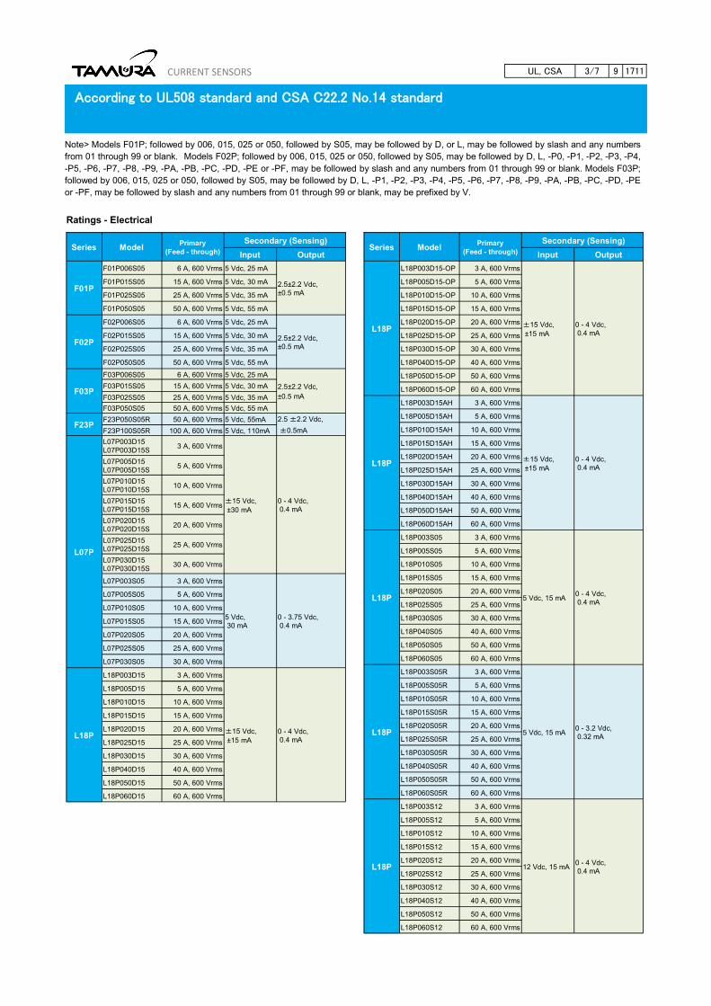
Ratings - Electrical
Series Model Primary
(Feed - through)
Secondary (Sensing)
Input Output
F01P
F01P006S05 6 A, 600 Vrms 5 Vdc, 25 mA
2.5±2.2 Vdc,
±0.5 mA
F01P015S05 15 A, 600 Vrms 5 Vdc, 30 mA
F01P025S05 25 A, 600 Vrms 5 Vdc, 35 mA
F01P050S05 50 A, 600 Vrms 5 Vdc, 55 mA
F02P
F02P006S05 6 A, 600 Vrms 5 Vdc, 25 mA
2.5±2.2 Vdc,
±0.5 mA
F02P015S05 15 A, 600 Vrms 5 Vdc, 30 mA
F02P025S05 25 A, 600 Vrms 5 Vdc, 35 mA
F02P050S05 50 A, 600 Vrms 5 Vdc, 55 mA
F03P F03P006S05 6 A, 600 Vrms 5 Vdc, 25 mA
2.5±2.2 Vdc,
±0.5 mA F03P015S05 15 A, 600 Vrms 5 Vdc, 30 mA
F03P025S05 25 A, 600 Vrms 5 Vdc, 35 mA
F03P050S05 50 A, 600 Vrms 5 Vdc, 55 mA
F23P F23P050S05R 50 A, 600 Vrms 5 Vdc, 55mA 2.5 ±2.2 Vdc,
±0.5mA F23P100S05R 100 A, 600 Vrms 5 Vdc, 110mA
L07P
L07P003D15
L07P003D15S 3 A, 600 Vrms
±15 Vdc,
±30 mA
0 - 4 Vdc,
0.4 mA
L07P005D15
L07P005D15S 5 A, 600 Vrms
L07P010D15
L07P010D15S 10 A, 600 Vrms
L07P015D15
L07P015D15S 15 A, 600 Vrms
L07P020D15
L07P020D15S 20 A, 600 Vrms
L07P025D15
L07P025D15S 25 A, 600 Vrms
L07P030D15
L07P030D15S 30 A, 600 Vrms
L07P003S05 3 A, 600 Vrms
5 Vdc,
30 mA
0 - 3.75 Vdc,
0.4 mA
L07P005S05 5 A, 600 Vrms
L07P010S05 10 A, 600 Vrms
L07P015S05 15 A, 600 Vrms
L07P020S05 20 A, 600 Vrms
L07P025S05 25 A, 600 Vrms
L07P030S05 30 A, 600 Vrms
L18P
L18P003D15 3 A, 600 Vrms
±15 Vdc,
±15 mA
0 - 4 Vdc,
0.4 mA
L18P005D15 5 A, 600 Vrms
L18P010D15 10 A, 600 Vrms
L18P015D15 15 A, 600 Vrms
L18P020D15 20 A, 600 Vrms
L18P025D15 25 A, 600 Vrms
L18P030D15 30 A, 600 Vrms
L18P040D15 40 A, 600 Vrms
L18P050D15 50 A, 600 Vrms
L18P060D15 60 A, 600 Vrms
Series Model Primary
(Feed - through)
Secondary (Sensing)
Input Output
L18P
L18P003D15-OP 3 A, 600 Vrms
±15 Vdc,
±15 mA
0 - 4 Vdc,
0.4 mA
L18P005D15-OP 5 A, 600 Vrms
L18P010D15-OP 10 A, 600 Vrms
L18P015D15-OP 15 A, 600 Vrms
L18P020D15-OP 20 A, 600 Vrms
L18P025D15-OP 25 A, 600 Vrms
L18P030D15-OP 30 A, 600 Vrms
L18P040D15-OP 40 A, 600 Vrms
L18P050D15-OP 50 A, 600 Vrms
L18P060D15-OP 60 A, 600 Vrms
L18P
L18P003D15AH 3 A, 600 Vrms
±15 Vdc,
±15 mA
0 - 4 Vdc,
0.4 mA
L18P005D15AH 5 A, 600 Vrms
L18P010D15AH 10 A, 600 Vrms
L18P015D15AH 15 A, 600 Vrms
L18P020D15AH 20 A, 600 Vrms
L18P025D15AH 25 A, 600 Vrms
L18P030D15AH 30 A, 600 Vrms
L18P040D15AH 40 A, 600 Vrms
L18P050D15AH 50 A, 600 Vrms
L18P060D15AH 60 A, 600 Vrms
L18P
L18P003S05 3 A, 600 Vrms
5 Vdc, 15 mA 0 - 4 Vdc,
0.4 mA
L18P005S05 5 A, 600 Vrms
L18P010S05 10 A, 600 Vrms
L18P015S05 15 A, 600 Vrms
L18P020S05 20 A, 600 Vrms
L18P025S05 25 A, 600 Vrms
L18P030S05 30 A, 600 Vrms
L18P040S05 40 A, 600 Vrms
L18P050S05 50 A, 600 Vrms
L18P060S05 60 A, 600 Vrms
L18P
L18P003S05R 3 A, 600 Vrms
5 Vdc, 15 mA 0 - 3.2 Vdc,
0.32 mA
L18P005S05R 5 A, 600 Vrms
L18P010S05R 10 A, 600 Vrms
L18P015S05R 15 A, 600 Vrms
L18P020S05R 20 A, 600 Vrms
L18P025S05R 25 A, 600 Vrms
L18P030S05R 30 A, 600 Vrms
L18P040S05R 40 A, 600 Vrms
L18P050S05R 50 A, 600 Vrms
L18P060S05R 60 A, 600 Vrms
L18P
L18P003S12 3 A, 600 Vrms
12 Vdc, 15 mA 0 - 4 Vdc,
0.4 mA
L18P005S12 5 A, 600 Vrms
L18P010S12 10 A, 600 Vrms
L18P015S12 15 A, 600 Vrms
L18P020S12 20 A, 600 Vrms
L18P025S12 25 A, 600 Vrms
L18P030S12 30 A, 600 Vrms
L18P040S12 40 A, 600 Vrms
L18P050S12 50 A, 600 Vrms
L18P060S12 60 A, 600 Vrms
Note> Models F01P; followed by 006, 015, 025 or 050, followed by S05, may be followed by D, or L, may be followed by slash and any numbers
from 01 through 99 or blank. Models F02P; followed by 006, 015, 025 or 050, followed by S05, may be followed by D, L, -P0, -P1, -P2, -P3, -P4,
-P5, -P6, -P7, -P8, -P9, -PA, -PB, -PC, -PD, -PE or -PF, may be followed by slash and any numbers from 01 through 99 or blank. Models F03P;
followed by 006, 015, 025 or 050, followed by S05, may be followed by D, L, -P1, -P2, -P3, -P4, -P5, -P6, -P7, -P8, -P9, -PA, -PB, -PC, -PD, -PE
or -PF, may be followed by slash and any numbers from 01 through 99 or blank, may be prefixed by V.

According to UL508 standard and CSA C22.2 No.14 standard
CURRENT SENSORS UL, CSA 4/7 9 1711
Ratings - Electrical
Series Model Primary
(Feed - through)
Secondary (Sensing)
Input Output
L18P
SL18P003D15 3 A, 600 Vrms
±15 Vdc,
±15 mA 0 - 4 Vdc,
0.4 mA
SL18P005D15 5 A, 600 Vrms
SL18P010D15 10 A, 600 Vrms
SL18P015D15 15 A, 600 Vrms
SL18P020D15 20 A, 600 Vrms
SL18P025D15 25 A, 600 Vrms
SL18P030D15 30 A, 600 Vrms
SL18P040D15 40 A, 600 Vrms
SL18P050D15 50 A, 600 Vrms
SL18P060D15 60 A, 600 Vrms
L18P
L18P003D15AHV 3 A, 600 Vrms
±15 Vdc,
±15 mA 0 - 4 Vdc,
0.4 mA
L18P005D15AHV 5 A, 600 Vrms
L18P010D15AHV 10 A, 600 Vrms
L18P015D15AHV 15 A, 600 Vrms
L18P020D15AHV 20 A, 600 Vrms
L18P025D15AHV 25 A, 600 Vrms
L18P030D15AHV 30 A, 600 Vrms
L18P040D15AHV 40 A, 600 Vrms
L18P050D15AHV 50 A, 600 Vrms
L18P060D15AHV 60 A, 600 Vrms
L18P003D15C 3 A, 600 Vrms
±15 Vdc,
±15 mA 0 - 4 Vdc,
0.4 mA L18P
L18P005D15C 5 A, 600 Vrms
L18P010D15C 10 A, 600 Vrms
L18P015D15C 15 A, 600 Vrms
L18P020D15C 20 A, 600 Vrms
L18P025D15C 25 A, 600 Vrms
L18P030D15C 30 A, 600 Vrms
L18P040D15C 40 A, 600 Vrms
L18P050D15C 50 A, 600 Vrms
L18P060D15C 60 A, 600 Vrms
L31S
L31S050S05S
L31S050S05FS 50 A, 600 Vrms
5 Vdc,
15 mA 1.875 - 3.125 Vdc,
0.3125 mA
L31S100S05S
L31S100S05FS 100 A, 600 Vrms
L31S200S05S
L31S200S05FS 200 A, 600 Vrms
L31S300S05S
L31S300S05FS 300 A, 600 Vrms
L31S400S05S
L31S400S05FS 400 A, 600 Vrms
L31S500S05S
L31S500S05FS 500 A, 600 Vrms
L31S600S05S
L31S600S05FS 600 A, 600 Vrms
L32P
L32P050S05FS
L32S050S05BFS 50 A, 600 Vrms
5 Vdc,
15 mA
1.875 - 3.125 Vdc,
0.3125 mA
L32P100S05FS
L32P100S05BFS 100 A, 600 Vrms
L32P150S05FS 150 A, 600 Vrms
L32P200S05FS 200 A, 600 Vrms
L32P300S05FS 300 A, 600 Vrms
L32P400S05FS 400 A, 600 Vrms
Series Model Primary
(Feed - through)
Secondary (Sensing)
Input Output
L34S
L34S200D15 L34S200D15C L34S200D15T
L34S200D15TC
200 A, 600 Vrms
±15 Vdc,
±25mA 0 - 4 Vdc, 0.4 mA
L34S300D15 L34S300D15C L34S300D15T
L34S300D15TC
300 A, 600 Vrms
L34S400D15 L34S400D15C L34S400D15T
L34S400D15TC
400 A, 600 Vrms
L34S500D15 L34S500D15C L34S500D15T
L34S500D15TC
500 A, 600 Vrms
L34S600D15 L34S600D15C L34S600D15T
L34S600D15TC
600 A, 600 Vrms
L34S1T0D15 L34S1T0D15C L34S1T0D15T
L34S1T0D15TC
1000 A, 600 Vrms
L34S1T2D15 L34S1T2D15C L34S1T2D15T
L34S1T2D15TC
1200 A, 600 Vrms
L34S1T5D15 L34S1T5D15C L34S1T5D15T
L34S1T5D15TC
1500 A, 600 Vrms
L37S
L37S050D15J L37S050D15M L37S050D15LJ
L37S050D15LM
50 A, 600 Vrms
±15 Vdc,
±25mA 0 - 4 Vdc, 0.4 mA
L37S100D15J L37S100D15M L37S100D15LJ
L37S100D15LM
100 A, 600 Vrms
L37S200D15J L37S200D15M L37S200D15LJ
L37S200D15LM
200 A, 600 Vrms
L37S300D15J L37S300D15M L37S300D15LJ
L37S300D15LM
300 A, 600 Vrms
L37S400D15J L37S400D15M L37S400D15LJ
L37S400D15LM
400 A, 600 Vrms
L37S500D15J L37S500D15M L37S500D15LJ
L37S500D15LM
500 A, 600 Vrms
L37S600S05J L37S600S05M L37S600S05LJ
600 A, 600 Vrms
L37S
L37S050S05J
L37S050S05M 50 A, 600 Vrms
5 Vdc, 20mA 0 - 4 Vdc, 0.4 mA
L37S100S05J
L37S100S05M 100 A, 600 Vrms
L37S200S05J
L37S200S05M 200 A, 600 Vrms
L37S300S05J
L37S300S05M 300 A, 600 Vrms
L37S400S05J
L37S400S05M 400 A, 600 Vrms
L37S500S05J
L37S500S05M 500 A, 600 Vrms
L37S600S05J
L37S600S05M 600 A, 600 Vrms
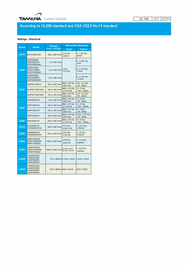
According to UL508 standard and CSA C22.2 No.14 standard
CURRENT SENSORS UL, CSA 5/7 9 1711
Ratings - Electrical
Series Model Primary
(Feed - through)
Secondary (Sensing)
Input Output
S21S S21S180D15JN 180 A, 600 Vrms ±15 Vdc,
±25mA
0 - 1.35 Vdc,
45mA
S22P
S22P006S05 S22P006S05P
S22P006S05M2 6 A, 600 Vrms
5 Vdc,
12.5 mA
0 - 3.125 Vdc,
3mA
S22P015S05 S22P015S05P
S22P015S05M2 15 A, 600 Vrms
0 - 3.125 Vdc,
7.5mA
S22P025S05 S22P025S05P
S22P025S05M2 25 A, 600 Vrms
0 - 3.125 Vdc,
12.5mA
S23P
S23P50/100D15 100 A, 600 Vrms MAX. ±15 Vdc,
±62.5 mA
-2.5 - 2.5 Vdc;
-50 - 50mA
S23P50/100D15M1 100 A, 600 Vrms MAX. ±15 Vdc,
±112.5 mA
-5 - 5 Vdc;
-100 - 100mA
S23P50/100D15M2 100 A, 600 Vrms MAX. ±15 Vdc,
±62.5 mA
-2.5 - 2.5 Vdc;
-50 - 50mA
S25P
S25P050D15X 50 A, 600 Vrms MAX. ±15 Vdc,
±62.5 mA
-5 - 5 Vdc;
-50 - 50mA
S25P100D15X 100 A, 600 Vrms MAX. ±15 Vdc,
±112.5 mA
-5 - 5 Vdc;
-100 - 100mA
S25P100D15Y 100 A, 600 Vrms MAX. ±15 Vdc,
±62.5 mA
-5 - 5 Vdc;
-50 - 50mA
S25P150D15Y 150 A, 600 Vrms MAX. ±15 Vdc,
±87.5 mA
-3.75 - 3.75 Vdc;
-75 - 75mA
S26P S26P200D15Y 200 A, 600 Vrms MAX. ±15 Vdc,
±112.5 mA
-5 - 5 Vdc;
-100 - 100mA
S27S S27S300D15Y
S27S300D15YM 300 A, 600 Vrms
±15 Vdc,
±162.5 mA
0 - ±7.5 Vdc,
±150mA
S28S S28S500D24Z
S28S500D24ZM 500 A, 600 Vrms
±24 Vdc,
±130 mA
0 - ±5 Vdc,
±100mA
S29S S29S1T0D24Z S29S1T0D24ZM
S29S1T0D24ZJ 1000 A, 600 Vrms
±24 Vdc,
±235 mA 0 - ±10 Vdc,
±200mA
S30S S30S2T0D24Z S30S2T0D24ZM
S30S2T0D24ZJ 2000 A, 600 Vrms
24 Vdc, 45 mA; -24 Vdc, -45 mA
0 - ±10 Vdc,
±400mA
LA02P
LA02P021S03 LA02P035S03 LA02P054S03
LA02P085S03
50 A, 480Vac 3.3Vdc, 0.5mA 3.3Vdc, 0.5mA
LA03P
LA03P021S05 LA03P035S05 LA03P054S05
LA03P085S05
50 A, 480Vac 5Vdc, 0.5mA 5Vdc, 0.5mA

According to UL508 standard and CSA C22.2 No.14 standard
CURRENT SENSORS UL, CSA 6/7 9 1711
Note> Models F01P; followed by 006, 015, 025 or 050, followed by S05, may be followed by D, or L, may be followed by slash and any numbers
from 01 through 99 or blank. Models F02P; followed by 006, 015, 025 or 050, followed by S05, may be followed by D, L, -P0, -P1, -P2, -P3, -P4,
-P5, -P6, -P7, -P8, -P9, -PA, -PB, -PC, -PD, -PE or -PF, may be followed by slash and any numbers from 01 through 99 or blank. Models F03P;
followed by 006, 015, 025 or 050, followed by S05, may be followed by D, L, -P1, -P2, -P3, -P4, -P5, -P6, -P7, -P8, -P9, -PA, -PB, -PC, -PD, -PE
or -PF, may be followed by slash and any numbers from 01 through 99 or blank, may be prefixed by V.
CAUTION
Series Model CAUTION / Notice
F01P F01P∗∗∗S05
- / Notice: The maximum temperature at top of case shall not be higher than 110°C and
busbar shall not be higher than 108°C in the end-use product. F02P F02P∗∗∗S05
F03P F03P∗∗∗S05
F23P F23P∗∗∗S05R - / Notice: The devices have been evaluated with the provision of the two cupper conduc-
tor-cum-heat sink as the primary conductor, measured 100 by 85 mm, 0.5 mm thick.
L07P
L07P∗∗∗D15
L07P∗∗∗D15S
L07P∗∗∗S05
- / -
L18P
L18P∗∗∗D15
L18P∗∗∗D15C
L18P∗∗∗D15-OP
L18P∗∗∗D15AH
L18P∗∗∗S05
L18P∗∗∗S05R
L18P∗∗∗S12
SL18P∗∗∗D15
L18P∗∗∗D15AHV
- / -
L31S L31S∗∗∗S05S
L31S∗∗∗S05FS - / Notice: Do not wrap the primary conductor around the core part of the product for pre-
venting to reduce the required Spacings.
L32P L32P∗∗∗S05(B)FS - / Notice: Do not wrap the primary conductor around the core part of the product for pre-
venting to reduce the required Spacings. The maximum temperature at case should not exceed 150˚C by the case’s insulation performance.
L34S
L34S∗∗∗D15
L34S∗∗∗D15C
L34S∗∗∗D15T
L34S∗∗∗D15TC
CAUTION: Do not wrap the primary conductor around the core part of
the product for preventing to reduce the required Spacings. / For models
with suffix T in Temperature Rating designation detailed in NOMENCLATURE for models in L34S series and L34SC series, the maximum temperature of the bus bar (primary con-ductor) shall not exceed 135°C at the end-use application.
L37S
L37S∗∗∗D15J
L37S∗∗∗D15M
L37S∗∗∗D15LJ
L37S∗∗∗D15LM
L37S∗∗∗S05J
L37S∗∗∗S05M
- / Notice: The housing of the female connector provided by the end-product shall be eval-
uated as a barrier under the end-application Standard in the end-use application, in case the clearance and/or the creepage distance do not meet the requirements of the end-application Standard. The maximum temperature of busbar shall not be higher than 102.3°C respectively at the end-use application.
LA02P LA02P∗∗∗S03 - / -
LA03P LA03P∗∗∗S05 - / -
The descriptions are directed from UL.

According to UL508 standard and CSA C22.2 No.14 standard
CURRENT SENSORS UL, CSA 7/7 9 1711
CAUTION
Series Model CAUTION / Notice
S21S S21S180D15JN CAUTION: Do not wrap the primary conductor around the core part of
the product to increase measured current. / -
S22P
S22P∗∗∗S05
S22P∗∗∗S05P
S22P∗∗∗S05M2
- / -
S23P
S23P50/100D15 S23P50/100D15M1 S23P50/100D15M2
CAUTION: Provide two min. 100 by 85 mm, 0.5mm thick cupper con-ductor-cum- heat sink as primary conductor of each side for safe us-age. / Notice : The primary conductor temperature and PCB should not exceed 100˚C by
the temperature regulations of internal parts.
S25P S25P∗∗∗D15∗ CAUTION: Do not wrap the primary conductor around the core part of the product to increase measured current. / -
S26P S26P200D15Y CAUTION: Do not wrap the primary conductor around the core part of the product to increase measured current. / -
S27S S27S300D15Y S27S300D15YM
- / Notice: Do not wrap the primary conductor around the core part of the product for pre-
venting to reduce the required Spacings.
S28S S28S500D24Z S28S500D24ZM
- / Notice: Do not wrap the primary conductor around the core part of the product for pre-
venting to reduce the required Spacings. The maximum temperature at case should not exceed 140˚C by the case’s insulation performance.
S29S
S29S1T0D24Z S29S1T0D24ZM S29S1T0D24ZJ
- / Notice: Do not wrap the primary conductor around the core part of the product for pre-
venting to reduce the required Spacings. The primary conductor temperature should not exceed 95˚C by the temperature regulations of internal parts.
S30S
S30S2T0D24Z S30S2T0D24ZM S30S2T0D24ZJ
- / Notice: These devices have been evaluated with the bus bar cooled by Liquid CPU
cooler, Type ELC-LMR240-BS manufactured by Enermax Technology Corporation. Based on this effect, the temperature of the bus bar was kept at 116.0˚C. Other than this usage, an additional evaluation shall be considered and conducted in the end-use application.
The descriptions are directed from UL.

F01P S05L, F02P S05L, F03P S05L SERIES
Fluxgate system / Voltage-output type, Anti-Surge current, Compact
RoHS
F01PxxxS05L F02PxxxS05L F03PxxxS05L
12.7
3-φ0.9
6-φ1.2
2.54×2=5.0813.4
2.54×2=5.0813.4
2.54×2=5.0810
12.7 12.7 12.7
2.542.54
7.62
1.11
2.542.54
7.62
7.62
2.54
2.54
7.62
2.542.54
1.16
F01PxxxS05LS22PxxxS05
S22PxxxS05M2 F01PxxxS05 S�� ������������
Reduced1�1��� �
Mounting areaThe mounting area has been reduced more than the F01P / F02P / F03PxxxS05 series. However, the F01P / F02P / F03PxxxS05L series series are 100% compatible with the F01P / F02P / F03PxxxS05series in regards to the footprint mounting.
• Backward compatible to F01PxxxS05, F02PxxxS05, F03PxxxS05 Series.• Anti-Surge current (4kAT,8/20uS, single)• Mounting area reduced, however, pin compatibility. Longitudinal dimension reduced.
• Super precision & High stability(Low temperature drift). • Unipolar power voltage; +5V. Rated Current; 6 〜 50A. Multi-range models. MAX_Temp.105℃ . Voltage-output type.• F01PxxxS05L series are designed by the pin compatibility as high- end models of S22PxxxS05M2 series.
Comparison of the main features
Series Features
F01PxxxS05L Without reference access.
F02PxxxS05L With reference access, Ref_in / Ref_out.
F03PxxxS05L With reference access, Ref_in / Ref_out. Higher creepage and clearance distances.
***: Rated Current symbol
SPECIFICATIONS
TypesSpec
Value
F01PxxxS05L F02PxxxS05L F03PxxxS05L
Maximum peak current 4kAT(2kA × 2. Number of primary tunes is two tunes.)
Rated Current If(xxx: Rated Current symbol) 6A(006) / 15A(015) / 25A(025) / 50A(050)
Maximum current( At Vcc=+5V, Ta=+105℃) ± 20A(If=6A) / ± 51A(If=15A) / ± 85A(If=25A) / ± 150A (If=50A)
Existence of reference access No Yes
Number of primary busbar 3pcs 4pcs
Clearance distance,Primary ⇔ Secondary 7.7mm 7.5mm 8.2mm
STANDARDS UL508(file № E243511), EN50178, EN61010-1, EN60950-1
Ambient operating temperature - 40℃ ~ +105℃
The F02P/F03PxxxS05L series also similarly reduces the mounting area.
The above-mentioned comparison tables are the auxiliary data for understanding each series. For details, please confirm the next page or subsequent ones. ▶▶▶
CURRENT SENSORS F01/02/03P S05L 2 16091/1
Intr
oduc
tion
Flux
gate
sys
tem
O
pen
loop
Cl
osed
loop
15

F01P L SERIES
Fluxgate system / Voltage-output type Anti-Surge current, Compact size
RoHS
ABSOLUTE MAXIMUM RATINGS
Parameters Symbol Unit Value Comment
Supply voltage Vcc V 7
Primary conductor temperature ― ℃ 110
ESD(HBM: Human Body Model) ― kV 4 C=100pF,R=1.5kΩ
Maximum peak current
― kAT 4
Current waveform: ・Front time 8µs ・Time to half value 20µs ・single
ISOLATION CHARACTERISTICS
Parameters Symbol Unit Value Comment
lnsulation voltage Vd ― AC4200V,for 1minute(Sensing current 0.5mA) Primary ⇔ Secondary
lnsulation Resistance RIS ― ≧ 500MΩ(at DC500V) Primary ⇔ Secondary
Clearance distance dCi ― 7.7mm(TYP) Primary ⇔ Secondary
Creepage distance dCp ― 7.7mm(TYP) Primary ⇔ Secondary
Case material ― ― UL94 V-0
Comparative Tracking Index;(CTI) CTI V 600
Application example― ― 300V,CAT Ⅲ,PD2
Reinforced isolation,non uniform field according to EN50178,EN61010
― ― 600V,CAT Ⅲ,PD2Reinforced isolation,non uniform field according to EN50178,EN61010
ENVIRONMENTAL AND MECHANICAL CHARACTERISTICS
Parameters Symbol UnitValue
CommentMIN TYP MAX
Ambient operating temperature Ta ℃ - 40 + 105
Ambient storage temperature Ts ℃ - 40 + 105
Mass m g 12
CURRENT SENSORS F01P L 2 14071/5
Intr
oduc
tion
Flux
gate
sys
tem
O
pen
loop
Cl
osed
loop
16

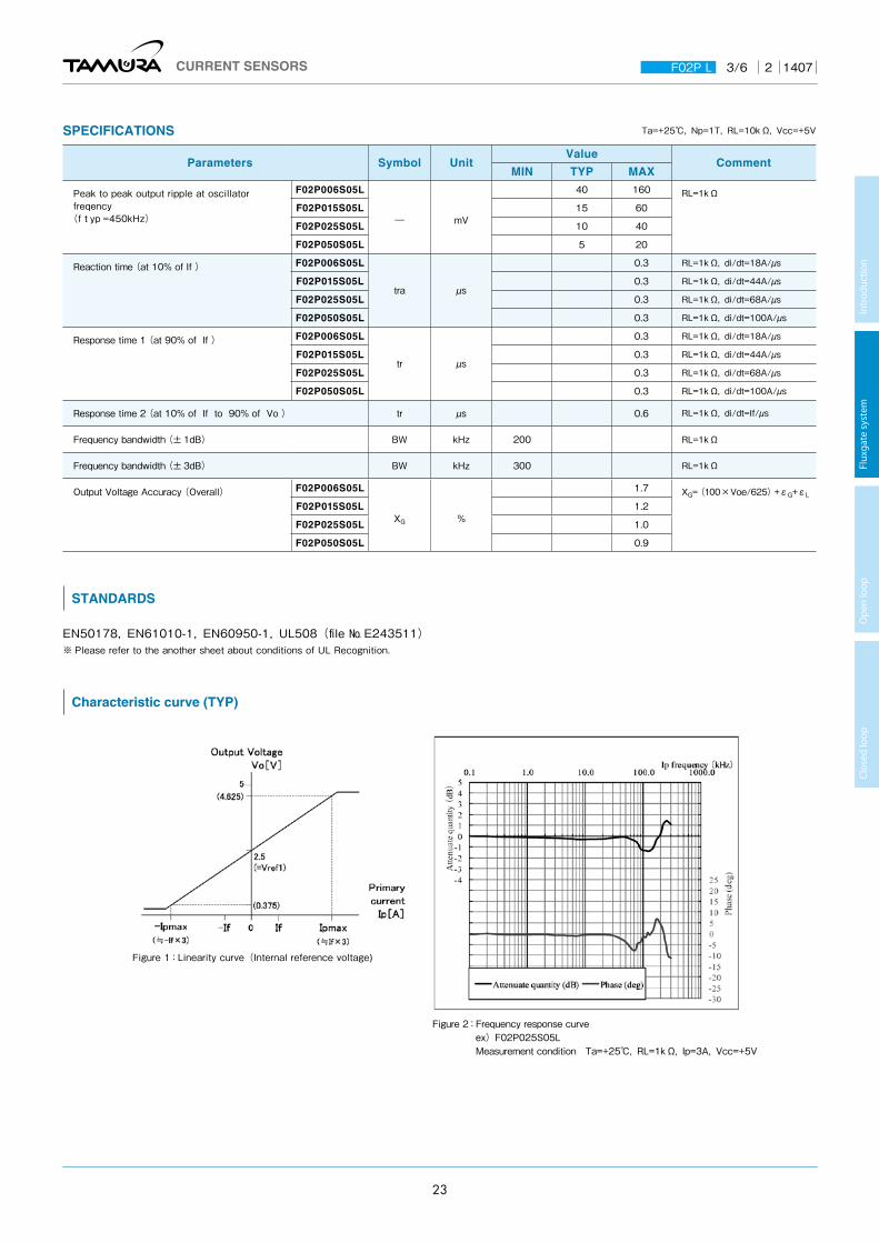
SPECIFICATIONS Ta=+25℃,Np=1T,RL=10kΩ,Vcc=+5V
Parameters Symbol UnitValue
CommentMIN TYP MAX
Rated Current F01P006S05L
If A
6
F01P015S05L 15
F01P025S05L 25
F01P050S05L 50
Maximum current (at Vcc= + 5V,Ta= + 105℃)
F01P006S05L
Ipmax A
- 20 20
F01P015S05L - 51 51
F01P025S05L - 85 85
F01P050S05L - 150 150
Supply Voltage Vcc V 4.75 5.00 5.25
Number of primary turns Np T 1,2,3
Number of secondary turns F01P006S05L
Ns T
1816
F01P015S05L 1737
F01P025S05L 1764
F01P050S05L 1600
Consumption current(at If) F01P006S05L
Icc mA
25 Icc=15 + Ip(mA)/ NsF01P015S05L 30
F01P025S05L 35
F01P050S05L 55
Output voltage Vo V 0.375 4.625
Output voltage(at Ip=0A) Vo V 2.5
Electrical offset voltage*1 F01P006S05L
Voe mV
- 10.40 10.40
F01P015S05L - 7.10 7.10
F01P025S05L - 6.25 6.25
F01P050S05L - 5.80 5.80
Electrical offset current reffered to primary F01P006S05L
Ioe A
- 0.10 0.10
F01P015S05L - 0.17 0.17
F01P025S05L - 0.25 0.25
F01P050S05L - 0.46 0.46
Temperature coefficient of Output voltage(at Ip=0A)
F01P006S05L
TCVo ppm/K
± 10.0 ± 80.0 ppm/K of 2.5V(- 40℃~+ 105℃)F01P015S05L ± 7.5 ± 70.0
F01P025S05L ± 6.5 ± 60.0
F01P050S05L ± 6.0 ± 60.0
Sensitivity(Theoretical value) F01P006S05L
Gth mV/A
104.2 625mV/IfF01P015S05L 41.67
F01P025S05L 25
F01P050S05L 12.5
Sensitivity error εG % - 0.7 0.7
Temperature coefficient of Sensitivity(at Ta= - 40℃~+ 105℃) TCG ppm/K ± 40
Output Linearity εL % - 0.1 0.1
Magnetic offset current reffered to primary(at 10×If) IOM A - 0.1 0.1
Output current noise reffered to primary(at 100Hz ~ 100kHz)
F01P006S05L
Ino µA/(Hz)1/2
36 RL=1kΩF01P015S05L 90
F01P025S05L 150
F01P050S05L 300
*1 Offset voltage value is after removal of core hysteresis.
CURRENT SENSORS F01P L 2 14072/5
Intr
oduc
tion
Flux
gate
sys
tem
O
pen
loop
Cl
osed
loop
17

Characteristic curve TYP
Figure 1:Linearity curve
Figure 2: Frequency response curve ex)F01P025S05L Measurement condition Ta=+25℃,RL=1kΩ,Ip=3A,Vcc=+5V
SPECIFICATIONS Ta=+25℃,Np=1T,RL=10kΩ,Vcc=+5V
Parameters Symbol UnitValue
CommentMIN TYP MAX
Peak to peak output ripple at oscillator freqency(f typ=450kHz)
F01P006S05L
― mV
40 160
RL=1kΩF01P015S05L 15 60
F01P025S05L 10 40
F01P050S05L 5 20
Reaction time(at 10% of If ) F01P006S05L
tra µs
0.3 RL=1kΩ,di/dt=18A/µs
F01P015S05L 0.3 RL=1kΩ,di/dt=44A/µs
F01P025S05L 0.3 RL=1kΩ,di/dt=68A/µs
F01P050S05L 0.3 RL=1kΩ,di/dt=100A/µs
Response time 1(at 90% of If ) F01P006S05L
tr µs
0.3 RL=1kΩ,di/dt=18A/µs
F01P015S05L 0.3 RL=1kΩ,di/dt=44A/µs
F01P025S05L 0.3 RL=1kΩ,di/dt=68A/µs
F01P050S05L 0.3 RL=1kΩ,di/dt=100A/µs
Response time 2(at 10% of If to 90% of Vo ) tr µs 0.6 RL=1kΩ,di/dt=If/µs
Frequency bandwidth(± 1dB) BW kHz 200 RL=1kΩ
Frequency bandwidth(± 3dB) BW kHz 300 RL=1kΩ
Output Voltage Accuracy(Overall) F01P006S05L
XG %
2.5 XG=(100×Voe/625)+εG+εL
F01P015S05L 1.9
F01P025S05L 1.8
F01P050S05L 1.7
STANDARDS
EN50178,EN61010-1,EN60950-1,UL508(file № E243511)※ Please refer to the another sheet about conditions of UL Recognition.
CURRENT SENSORS F01P L 2 14073/5
Intr
oduc
tion
Flux
gate
sys
tem
O
pen
loop
Cl
osed
loop
18

F01P006S05L Derating
F01P025S05L Derating
F01P015S05L Derating
F01P050S05L Derating
Maximum continuous DC primary current
Figure 3:Ip vs Ta for F01P006S05L
Figure 5:Ip vs Ta for F01P025S05L
According to which the following conditions are true the maximum continuous DC primary current plot shows the boundary of the area.
① Ip < Ipmax② Junction temperature Tj < 125℃③ Primary conductor temperature < 110℃④ Resistor power dissipation < 0.5 x rated power
Figure 4:Ip vs Ta for F01P015S05L
Figure 6:Ip vs Ta for F01P050S05L
AC Derating
Frequency derating
Figure 7: Maximum RMS AC primary current/maximum DC primary current vs frequency
SUPPORT DOCUMENTATION
CURRENT SENSORS F01P L 2 14074/5
Intr
oduc
tion
Flux
gate
sys
tem
O
pen
loop
Cl
osed
loop
19
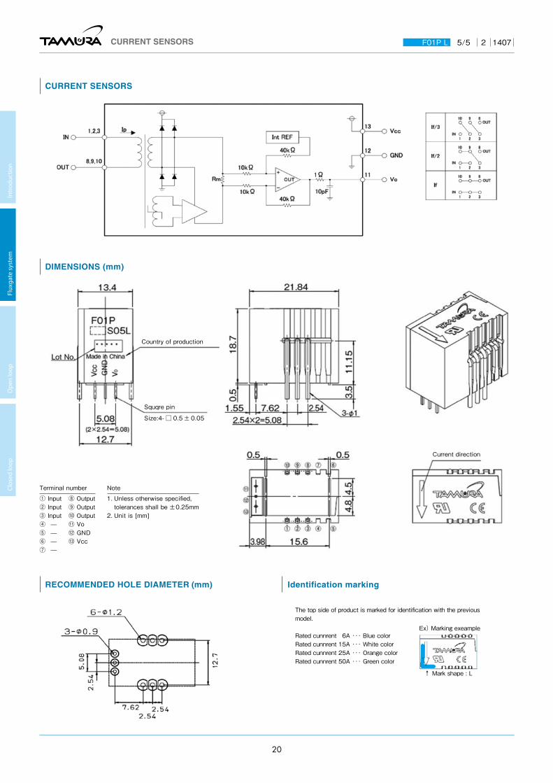
CURRENT SENSORS
Squqre pin
Current direction
Size:4- □ 0.5 ± 0.05
Country of production
Terminal number① Input ⑧ Output② Input ⑨ Output③ Input ⑩ Output④ — ⑪ Vo⑤ — ⑫ GND⑥ — ⑬ Vcc⑦ —
Note1. Unless otherwise specified,
tolerances shall be ±0.25mm2. Unit is [mm]
DIMENSIONS (mm)
The top side of product is marked for identification with the previous model.
Rated cunnrent 6A ・・・ Blue colorRated cunnrent 15A ・・・ White colorRated cunnrent 25A ・・・ Orange color Rated cunnrent 50A ・・・ Green color
Ex) Marking exeample
↑ Mark shape : L
RECOMMENDED HOLE DIAMETER (mm) Identification marking
CURRENT SENSORS F01P L 2 14075/5
Intr
oduc
tion
Flux
gate
sys
tem
O
pen
loop
Cl
osed
loop
20
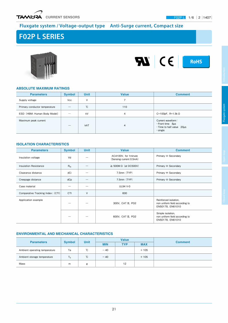
F02P L SERIES
Fluxgate system / Voltage-output type Anti-Surge current, Compact size
ABSOLUTE MAXIMUM RATINGS
Parameters Symbol Unit Value Comment
Supply voltage Vcc V 7
Primary conductor temperature ― ℃ 110
ESD(HBM: Human Body Model) ― kV 4 C=100pF,R=1.5kΩ
Maximum peak current
― kAT 4
Current waveform:・Front time 8µs・Time to half value 20µs・single
ENVIRONMENTAL AND MECHANICAL CHARACTERISTICS
Parameters Symbol UnitValue
CommentMIN TYP MAX
Ambient operating temperature Ta ℃ - 40 + 105
Ambient storage temperature TS ℃ - 40 + 105
Mass m g 12
ISOLATION CHARACTERISTICS
Parameters Symbol Unit Value Comment
lnsulation voltage Vd ― AC4100V,for 1minute(Sensing current 0.5mA)
Primary ⇔ Secondary
lnsulation Resistance RIS ― ≧ 500MΩ(at DC500V) Primary ⇔ Secondary
Clearance distance dCi ― 7.5mm(TYP) Primary ⇔ Secondary
Creepage distance dCp ― 7.5mm(TYP) Primary ⇔ Secondary
Case material ― ― UL94 V-0
Comparative Tracking Index; (CTI) CTI V 600
Application example― ― 300V,CAT Ⅲ,PD2
Reinforced isolation, non uniform field according to EN50178,EN61010
― ― 600V,CAT Ⅲ,PD2Simple isolation, non uniform field according to EN50178,EN61010
RoHS
CURRENT SENSORS F02P L 2 14071/6
Intr
oduc
tion
Flux
gate
sys
tem
O
pen
loop
Cl
osed
loop
21

SPECIFICATIONS Ta=+25℃,Np=1T,RL=10kΩ,Vcc=+5V
Parameters Symbol UnitValue
CommentMIN TYP MAX
Rated Current F02P006S05L
If A
6
F02P015S05L 15
F02P025S05L 25
F02P050S05L 50
Maximum current (at Vcc= + 5V,Ta= + 105℃)
F02P006S05L
Ipmax A
- 20 20
F02P015S05L - 51 51
F02P025S05L - 85 85
F02P050S05L - 150 150
Supply Voltage Vcc V 4.75 5.00 5.25
Number of primary turns Np T 1,2,3
Number of secondary turns F02P006S05L
Ns T
1816
F02P015S05L 1737
F02P025S05L 1764
F02P050S05L 1600
Consumption current (at If) F02P006S05L
Icc mA
25 Icc=15 + Ip(mA)/ NsF02P015S05L 30
F02P025S05L 35
F02P050S05L 55
Internal reference voltage(at Ip=0A) Vref1 V 2.495 2.500 2.505 Ref OUT mode
External reference voltage Vref2 V 0 4 Ref IN mode
Output voltage Vo V 0.375 4.625
Output voltage(at Ip=0A) Vo V Vref1,Vref2
Electrical offset voltage*1 F02P006S05L
Voe mV
- 5.300 5.300
F02P015S05L - 2.210 2.210
F02P025S05L - 1.350 1.350
F02P050S05L - 0.725 0.725
Electrical offset current reffered to primary F02P006S05L
Ioe mA
- 51 51
F02P015S05L - 53 53
F02P025S05L - 54 54
F02P050S05L - 58 58
Temperature coefficient of Internal reference voltage TCVref1 ppm/K ± 5.0 ± 50
Temperature coefficient of Output voltage (at Ip=0A)
F02P006S05L
TCVo ppm/K
± 6.0 ± 14 ppm/K of 2.5V (- 40℃~+ 105℃)F02P015S05L ± 2.3 ± 6
F02P025S05L ± 1.4 ± 4
F02P050S05L ± 0.7 ± 3
Sensitivity(Theoretical value) F02P006S05L
Gth mV/A
104.2 625mV/IfF02P015S05L 41.67
F02P025S05L 25
F02P050S05L 12.5
Sensitivity error εG % - 0.7 0.7
Temperature coefficient of Sensitivity (at Ta= - 40℃〜+ 105℃) TCG ppm/K ± 40
Output Linearity εL % - 0.1 0.1
Magnetic offset current reffered to primary (at 10×If) IOM A - 0.1 0.1
Output current noise reffered to primary (at 100Hz 〜 100kHz) Ino µA/(Hz)1/2 20 RL=1kΩ
*1 Offset voltage value is after removal of core hysteresis.
CURRENT SENSORS F02P L 2 14072/6
Intr
oduc
tion
Flux
gate
sys
tem
O
pen
loop
Cl
osed
loop
22
STANDARDS
EN50178,EN61010-1,EN60950-1,UL508(file № E243511)※ Please refer to the another sheet about conditions of UL Recognition.
Characteristic curve (TYP)
Figure 1:Linearity curve(Internal reference voltage)
Figure 2: Frequency response curve ex)F02P025S05L Measurement condition Ta=+25℃,RL=1kΩ,Ip=3A,Vcc=+5V
SPECIFICATIONS Ta=+25℃,Np=1T,RL=10kΩ,Vcc=+5V
Parameters Symbol UnitValue
CommentMIN TYP MAX
Peak to peak output ripple at oscillator freqency
(f typ=450kHz)
F02P006S05L
― mV
40 160 RL=1kΩF02P015S05L 15 60
F02P025S05L 10 40
F02P050S05L 5 20
Reaction time (at 10% of If ) F02P006S05L
tra µs
0.3 RL=1kΩ,di/dt=18A/µs
F02P015S05L 0.3 RL=1kΩ,di/dt=44A/µs
F02P025S05L 0.3 RL=1kΩ,di/dt=68A/µs
F02P050S05L 0.3 RL=1kΩ,di/dt=100A/µs
Response time 1 (at 90% of If ) F02P006S05L
tr µs
0.3 RL=1kΩ,di/dt=18A/µs
F02P015S05L 0.3 RL=1kΩ,di/dt=44A/µs
F02P025S05L 0.3 RL=1kΩ,di/dt=68A/µs
F02P050S05L 0.3 RL=1kΩ,di/dt=100A/µs
Response time 2 (at 10% of If to 90% of Vo ) tr µs 0.6 RL=1kΩ,di/dt=If/µs
Frequency bandwidth (± 1dB) BW kHz 200 RL=1kΩ
Frequency bandwidth (± 3dB) BW kHz 300 RL=1kΩ
Output Voltage Accuracy (Overall) F02P006S05L
XG %
1.7 XG=(100×Voe/625)+εG+εL
F02P015S05L 1.2
F02P025S05L 1.0
F02P050S05L 0.9
CURRENT SENSORS F02P L 2 14073/6
Intr
oduc
tion
Flux
gate
sys
tem
O
pen
loop
Cl
osed
loop
23

F02P006S05L Derating
F02P025S05L Derating
F02P015S05L Derating
F02P050S05L Derating
SUPPORT DOCUMENTATION
Maximum continuous DC primary current
Figure 3:Ip vs Ta for F02P006S05L
Figure 5:Ip vs Ta for F02P025S05L
According to which the following conditions are true the maximum continuous DC primary current plot shows the boundary of the area.
① Ip < Ipmax② Junction temperature Tj < 125℃③ Primary conductor temperature < 110℃④ Resistor power dissipation < 0.5 x rated power
Figure 4:Ip vs Ta for F02P015S05L
Figure 6:Ip vs Ta for F02P050S05L
AC Derating
Frequency derating
Figure 7: Maximum RMS AC primary current/maximum DC primary current vs frequency
CURRENT SENSORS F02P L 2 14074/6
Intr
oduc
tion
Flux
gate
sys
tem
O
pen
loop
Cl
osed
loop
24

Reference voltage
The Ref pin has two modes Ref IN and Ref OUT:
< Ref OUT mode >The 2.5V internal precision reference is used by the transducer as the reference point for bipolar measurements;
< Ref IN mode >An external reference voltage is connected to the Ref pin; this voltage is specified in the range 0 to 4 V , its voltage is used as the reference voltage at the time of measurement.
-either to source a typical current of (Vref - 2.5)/680,the maximum value will be 2.2mA typ.when Vref2 = 4V.-or to sink a typical current of (2.5 - Vref2)/680,the maximum value will be 3.68mA typ.when Vref2 = 0V.
The following graphs show how the measuring range of each transducer version depends on external reference voltage value Vref2.
F02P006S05L
F02P025S05L
F02P015S05L
F02P050S05L
Upper limit: Ip =- 9.6×Vref2 + 44.4 (Vref2 = 0...4V)
Lower limit: Ip =- 9.6×Vref2 + 3.6 (Vref2 = 0...4V)
Upper limit: Ip = 85 (Vref2 = 0...2.5V) Ip =- 40×Vref2 + 185 (Vref2 = 2.5...4V)
Lower limit: Ip =- 40×Vref2 + 15 (Vref2 = 0...2.5V) Ip =- 85 (Vref2 = 2.5...4V)
Upper limit: Ip = 80 (Vref2 = 0...1.29V) Ip =- 24×Vref2 + 111 (Vref2 = 1.29...4V)
Lower limit: Ip =- 24×Vref2 + 9 (Vref2 = 0...3.7V) Ip =- 80 (Vref2 = 3.7...4V)
Upper limit: Ip = 150 (Vref2 = 0...2.75V) Ip =- 80×Vref2 + 370 (Vref2 = 2.75...4V)
Lower limit: Ip =- 80×Vref2 + 30 (Vref2 = 0...2.25V) Ip =- 150 (Vref2 = 2.25...4V)
If you do not want to use the Ref pin, please unconnected.
CURRENT SENSORS F02P L 2 14075/6
Intr
oduc
tion
Flux
gate
sys
tem
O
pen
loop
Cl
osed
loop
25
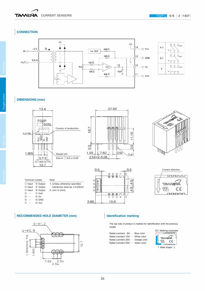
CONNECTION
RECOMMENDED HOLE DIAMETER (mm) Identification marking
The top side of product is marked for identification with the previous model.
Rated cunnrent 6A ・・・ Blue colorRated cunnrent 15A ・・・ White colorRated cunnrent 25A ・・・ Orange color Rated cunnrent 50A ・・・ Green color
Ex) Marking exeample
↑ Mark shape : L
Squqre pin
Current direction
Size:4- □ 0.5 ± 0.05
DIMENSIONS (mm)
Country of production
Terminal number
① Input ⑧ Output② Input ⑨ Output③ Input ⑩ Output④ — ⑪ Vref⑤ — ⑫ Vo⑥ — ⑬ GND⑦ — ⑭ Vcc
Note
1. Unless otherwise specified, tolerances shall be ±0.25mm
2. Unit is [mm]
CURRENT SENSORS F02P L 2 14076/6
Intr
oduc
tion
Flux
gate
sys
tem
O
pen
loop
Cl
osed
loop
26

F03P L SERIES
Fluxgate system / Voltage-output type Anti-Surge current, Compact size
ABSOLUTE MAXIMUM RATINGS
Parameters Symbol Unit Value Comment
Supply voltage Vcc V 7
Primary conductor temperature ― ℃ 110
ESD(HBM: Human Body Model) ― kV 4 C=100pF, R=1.5kΩ
Maximum peak current
― kAT 4
Current waveform:・Front time 8µs ・Time to half value 20µs ・single
ENVIRONMENTAL AND MECHANICAL CHARACTERISTICS
Parameters Symbol UnitValue
CommentMIN TYP MAX
Ambient operating temperature Ta ℃ - 40 + 105
Ambient storage temperature TS ℃ - 40 + 105
Mass m g 12
ISOLATION CHARACTERISTICS
Parameters Symbol Unit Value Comment
lnsulation voltage Vd ― AC4300V,for 1minute(Sensing current 0.5mA) Primary ⇔ Secondary
lnsulation Resistance RIS ― ≧ 500MΩ(at DC500V) Primary ⇔ Secondary
Clearance distance dCi ― 8.2mm(TYP) Primary ⇔ Secondary
Creepage distance dCp ― 8.2mm(TYP) Primary ⇔ Secondary
Case material ― ― UL94 V-0
Comparative Tracking Index;(CTI) CTI V 600
Application example ― ― 300V,CAT Ⅲ,PD2 Reinforced isolation,non uniform field according to EN61010
― ― 600V,CAT Ⅲ,PD2 Reinforced isolation,non uniform field according to EN50178
― ― 1000V,CAT Ⅲ,PD2 Simple isolation,non uniform field according to EN50178
RoHS
CURRENT SENSORS F03P L 2 14071/6
Intr
oduc
tion
Flux
gate
sys
tem
O
pen
loop
Cl
osed
loop
27

SPECIFICATIONS Ta=+25℃,Np=1T,RL=10kΩ,Vcc=+5V
Parameters Symbol UnitValue
CommentMIN TYP MAX
Rated Current F03P006S05L
If A
6
F03P015S05L 15
F03P025S05L 25
F03P050S05L 50
Maximum current F03P006S05L
Ipmax A
- 20 20
F03P015S05L - 51 51
F03P025S05L - 85 85
F03P050S05L - 150 150
Supply Voltage Vcc V 4.75 5.00 5.25
Number of primary turns Np T 1,2,3,4
Number of secondary turns F03P006S05L
Ns T
1816
F03P015S05L 1737
F03P025S05L 1764
F03P050S05L 1600
Consumption current(at If) F03P006S05L
Icc mA
25 Icc = 15 + Ip(mA)/ NsF03P015S05L 30
F03P025S05L 35
F03P050S05L 55
Internal reference voltage(at Ip = 0A) Vref1 V 2.495 2.500 2.505 Ref OUT mode
External reference voltage Vref2 V 0 4 Ref IN mode
Output voltage Vo V 0.375 4.625
Output voltage(at Ip = 0A) Vo V Vref1,Vref2
Electrical offset voltage*1 F03P006S05L
Voe mV
- 5.300 5.300
F03P015S05L - 2.210 2.210
F03P025S05L - 1.350 1.350
F03P050S05L - 0.725 0.725
Electrical offset current reffered to primary F03P006S05L
Ioe mA
- 51 51
F03P015S05L - 53 53
F03P025S05L - 54 54
F03P050S05L - 58 58
Temperature coefficient of Internal reference voltage TCVref1 ppm/K ± 5.0 ± 50
Temperature coefficient of Output voltage(at Ip = 0A)
F03P006S05L
TCVo ppm/K
± 6.0 ± 14 ppm/K of 2.5V(- 40℃~+ 105℃)F03P015S05L ± 2.3 ± 6
F03P025S05L ± 1.4 ± 4
F03P050S05L ± 0.7 ± 3
Sensitivity(Theoretical value) F03P006S05L
Gth mV/A
104.2 625mV/IfF03P015S05L 41.67
F03P025S05L 25
F03P050S05L 12.5
Sensitivity error εG % - 0.7 0.7
Temperature coefficient of Sensitivity(at Ta =- 40℃〜+ 105℃) TCG ppm/K ± 40
Output Linearity(at If) εL % - 0.1 0.1
Magnetic offset current reffered to primary(at 10×If) IOM A - 0.1 0.1
Output current noise reffered to primary(at 100Hz 〜 100kHz) Ino µA/(Hz)1/2 20 RL = 1kΩ
*1 Offset voltage value is after removal of core hysteresis.
CURRENT SENSORS F03P L 2 14072/6
Intr
oduc
tion
Flux
gate
sys
tem
O
pen
loop
Cl
osed
loop
28
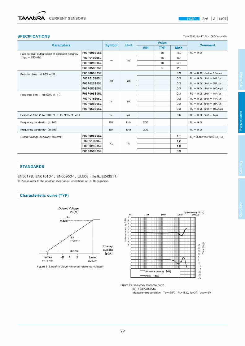
STANDARDS
EN50178,EN61010-1,EN60950-1,UL508(file № E243511)※ Please refer to the another sheet about conditions of UL Recognition.
Characteristic curve (TYP)
Figure 1:Linearity curve(Internal reference voltage)
Figure 2: Frequency response curve ex)F03P025S05L Measurement condition Ta=+25℃,RL=1kΩ,Ip=3A,Vcc=+5V
SPECIFICATIONS Ta=+25℃,Np=1T,RL=10kΩ,Vcc=+5V
Parameters Symbol UnitValue
CommentMIN TYP MAX
Peak to peak output ripple at oscillator freqency(f typ = 450kHz)
F03P006S05L
― mV
40 160 RL = 1kΩ
F03P015S05L 15 60
F03P025S05L 10 40
F03P050S05L 5 20
Reaction time(at 10% of If ) F03P006S05L
tra µs
0.3 RL = 1kΩ,di/dt = 18A/µs
F03P015S05L 0.3 RL = 1kΩ,di/dt = 44A/µs
F03P025S05L 0.3 RL = 1kΩ,di/dt = 68A/µs
F03P050S05L 0.3 RL = 1kΩ,di/dt = 100A/µs
Response time 1(at 90% of If ) F03P006S05L
tr µs
0.3 RL = 1kΩ,di/dt = 18A/µs
F03P015S05L 0.3 RL = 1kΩ,di/dt = 44A/µs
F03P025S05L 0.3 RL = 1kΩ,di/dt = 68A/µs
F03P050S05L 0.3 RL = 1kΩ,di/dt = 100A/µs
Response time 2(at 10% of If to 90% of Vo ) tr µs 0.6 RL = 1kΩ,di/dt = If/µs
Frequency bandwidth(± 1dB) BW kHz 200 RL = 1kΩ
Frequency bandwidth(± 3dB) BW kHz 300 RL = 1kΩ
Output Voltage Accuracy(Overall) F03P006S05L
XG %
1.7 XG=(100×Voe/625)+εG+εL
F03P015S05L 1.2
F03P025S05L 1.0
F03P050S05L 0.9
CURRENT SENSORS F03P L 2 14073/6
Intr
oduc
tion
Flux
gate
sys
tem
O
pen
loop
Cl
osed
loop
29

F03P006S05L Derating
F03P025S05L Derating
F03P015S05L Derating
F03P050S05L Derating
SUPPORT DOCUMENTATION
Maximum continuous DC primary current
Figure 3:Ip vs Ta for F03P006S05L
Figure 5:Ip vs Ta for F03P025S05L
According to which the following conditions are true the maximum continuous DC primary current plot shows the boundary of the area.
① Ip < Ipmax② Junction temperature Tj < 125℃③ Primary conductor temperature < 110℃④ Resistor power dissipation < 0.5 x rated power
Figure 4:Ip vs Ta for F03P015S05L
Figure 6:Ip vs Ta for F03P050S05L
Frequency derating
Figure 7: Maximum RMS AC primary current/maximum DC primary current vs frequency
CURRENT SENSORS F03P L 2 14074/6
Intr
oduc
tion
Flux
gate
sys
tem
O
pen
loop
Cl
osed
loop
30
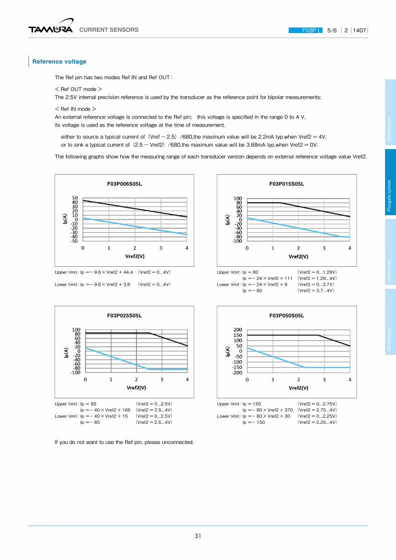
Reference voltage
The Ref pin has two modes Ref IN and Ref OUT:
< Ref OUT mode >The 2.5V internal precision reference is used by the transducer as the reference point for bipolar measurements;
< Ref IN mode > An external reference voltage is connected to the Ref pin; this voltage is specified in the range 0 to 4 V, its voltage is used as the reference voltage at the time of measurement.
-either to source a typical current of(Vref - 2.5)/680,the maximum value will be 2.2mA typ.when Vref2 = 4V.-or to sink a typical current of(2.5 - Vref2)/680,the maximum value will be 3.68mA typ.when Vref2 = 0V.
The following graphs show how the measuring range of each transducer version depends on external reference voltage value Vref2.
F03P006S05L
F03P025S05L
F03P015S05L
F03P050S05L
Upper limit:Ip =- 9.6×Vref2 + 44.4 (Vref2 = 0...4V) Lower limit:Ip =- 9.6×Vref2 + 3.6 (Vref2 = 0...4V)
Upper limit: Ip = 85 (Vref2 = 0...2.5V) Ip =- 40×Vref2 + 185 (Vref2 = 2.5...4V)
Lower limit: Ip =- 40×Vref2 + 15 (Vref2 = 0...2.5V) Ip =- 85 (Vref2 = 2.5...4V)
Upper limit: Ip = 80 (Vref2 = 0...1.29V) Ip =- 24×Vref2 + 111 (Vref2 = 1.29...4V)
Lower limit: Ip =- 24×Vref2 + 9 (Vref2 = 0...3.7V) Ip =- 80 (Vref2 = 3.7...4V)
Upper limit: Ip = 150 (Vref2 = 0...2.75V) Ip =- 80×Vref2 + 370 (Vref2 = 2.75...4V)
Lower limit: Ip =- 80×Vref2 + 30 (Vref2 = 0...2.25V) Ip =- 150 (Vref2 = 2.25...4V)
If you do not want to use the Ref pin, please unconnected.
CURRENT SENSORS F03P L 2 14075/6
Intr
oduc
tion
Flux
gate
sys
tem
O
pen
loop
Cl
osed
loop
31

Squqre pin
Current direction
Size:4- □ 0.5 ± 0.05
DIMENSIONS (mm)
Country of production
Terminal number
① — ⑧ Output② Input ⑨ Output③ Input ⑩ —④ Input ⑪ Vref ⑤ Input ⑫ Vo⑥ Output ⑬ GND⑦ Output ⑭ Vcc
Note
1. Unless otherwise specified, tolerances shall be ±0.25mm
2. Unit is [mm]
CONNECTION
RECOMMENDED HOLE DIAMETER (mm) Identification marking
The top side of product is marked for identification with the previous model.
Rated cunnrent 6A ・・・ Blue colorRated cunnrent 15A ・・・ White colorRated cunnrent 25A ・・・ Orange color Rated cunnrent 50A ・・・ Green color
Ex) Marking exeample
↑ Mark shape : L
CURRENT SENSORS F03P L 2 14076/6
Intr
oduc
tion
Flux
gate
sys
tem
O
pen
loop
Cl
osed
loop
32
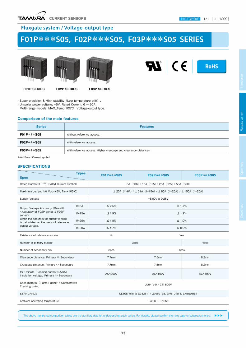
F01P***S05, F02P***S05, F03P***S05 SERIES
Fluxgate system / Voltage-output type
• Super precision & High stability(Low temperature drift). • Unipolar power voltage; +5V. Rated Current; 6 〜 50A. Multi-range models. MAX_Temp.105℃ . Voltage-output type.
Comparison of the main features
Series Features
F01P***S05 Without reference access.
F02P***S05 With reference access.
F03P***S05 With reference access. Higher creepage and clearance distances.
***:Rated Current symbol
F01P SERIES F02P SERIES F03P SERIES
SPECIFICATIONS
TypesSpec
F01P***S05 F02P***S05 F03P***S05
Rated Current If (***: Rated Current symbol) 6A(006) / 15A(015) / 25A(025) / 50A(050)
Maximum current(At Vcc=+5V, Ta=+105℃) ± 20A(If=6A) / ± 51A(If=15A) / ± 85A(If=25A) / ± 150A(If=25A)
Supply Voltage +5.00V ± 0.25V
Output Voltage Accuracy (Overall)<Accuracy of F02P series & F03P series> When the accuracy of output voltage is calculated on the basis of reference output voltage.
If=6A ≦ 2.5% ≦ 1.7%
If=15A ≦ 1.9% ≦ 1.2%
If=25A ≦ 1.8% ≦ 1.0%
If=50A ≦ 1.7% ≦ 0.9%
Existence of reference access No Yes
Number of primary busbar 3pcs 4pcs
Number of secondary pin 3pcs 4pcs
Clearance distance, Primary ⇔ Secondary 7.7mm 7.5mm 8.2mm
Creepage distance, Primary ⇔ Secondary 7.7mm 7.5mm 8.2mm
for 1minute (Sensing current 0.5mA) lnsulation voltage,Primary ⇔ Secondary AC4200V AC4100V AC4300V
Case material (Flame Rating) / Comparative Tracking Index; UL94 V-0 / CTI 600V
STANDARDS UL508(file № E243511),EN50178, EN61010-1, EN60950-1
Ambient operating temperature - 40℃ ~ +105℃
The above-mentioned comparison tables are the auxiliary data for understanding each series. For details, please confirm the next page or subsequent ones. ▶▶▶
RoHS
CURRENT SENSORS F01P/F02P/F03P 1 12091/1
Intr
oduc
tion
Flux
gate
sys
tem
O
pen
loop
Cl
osed
loop
33
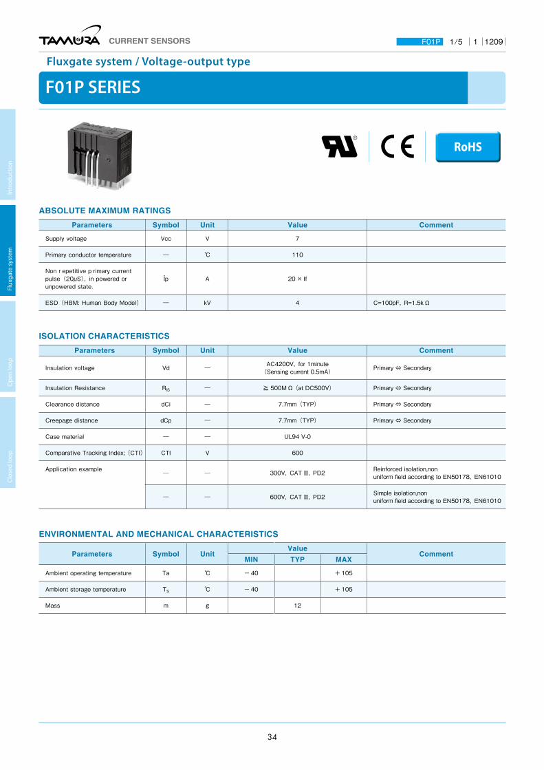
F01P SERIES
Fluxgate system / Voltage-output type
ABSOLUTE MAXIMUM RATINGS
Parameters Symbol Unit Value Comment
Supply voltage Vcc V 7
Primary conductor temperature ― ℃ 110
Non repetitive primary current pulse(20µS),in powered or unpowered state.
Îp A 20 × If
ESD(HBM: Human Body Model) ― kV 4 C=100pF,R=1.5kΩ
ENVIRONMENTAL AND MECHANICAL CHARACTERISTICS
Parameters Symbol UnitValue
CommentMIN TYP MAX
Ambient operating temperature Ta ℃ - 40 + 105
Ambient storage temperature TS ℃ - 40 + 105
Mass m g 12
ISOLATION CHARACTERISTICS
Parameters Symbol Unit Value Comment
lnsulation voltage Vd ― AC4200V,for 1minute(Sensing current 0.5mA) Primary ⇔ Secondary
lnsulation Resistance RIS ― ≧ 500MΩ(at DC500V) Primary ⇔ Secondary
Clearance distance dCi ― 7.7mm(TYP) Primary ⇔ Secondary
Creepage distance dCp ― 7.7mm(TYP) Primary ⇔ Secondary
Case material ― ― UL94 V-0
Comparative Tracking Index; (CTI) CTI V 600
Application example ― ― 300V,CAT Ⅲ,PD2 Reinforced isolation,non uniform field according to EN50178,EN61010
― ― 600V,CAT Ⅲ,PD2 Simple isolation,non uniform field according to EN50178,EN61010
RoHS
CURRENT SENSORS F01P 1 12091/5
Intr
oduc
tion
Flux
gate
sys
tem
O
pen
loop
Cl
osed
loop
34
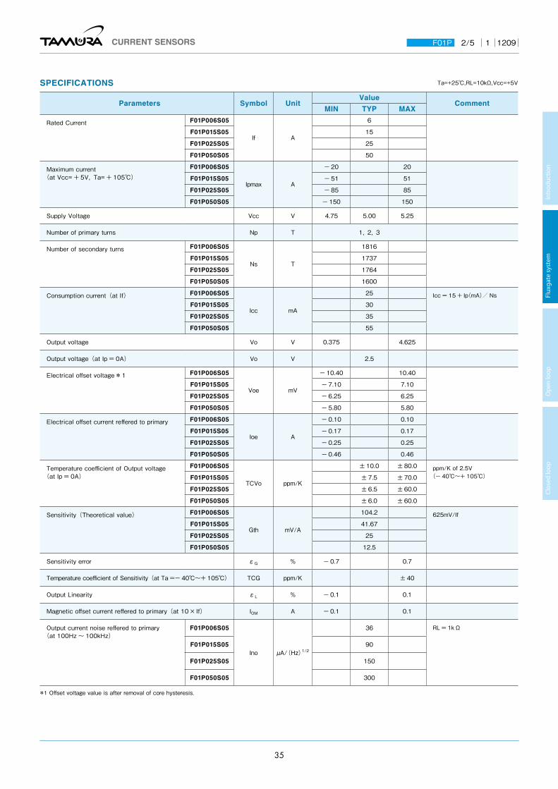
SPECIFICATIONS Ta=+25℃,RL=10kΩ,Vcc=+5V
Parameters Symbol UnitValue
CommentMIN TYP MAX
Rated Current F01P006S05
If A
6
F01P015S05 15
F01P025S05 25
F01P050S05 50
Maximum current(at Vcc= + 5V,Ta= + 105℃)
F01P006S05
Ipmax A
- 20 20
F01P015S05 - 51 51
F01P025S05 - 85 85
F01P050S05 - 150 150
Supply Voltage Vcc V 4.75 5.00 5.25
Number of primary turns Np T 1,2,3
Number of secondary turns F01P006S05
Ns T
1816
F01P015S05 1737
F01P025S05 1764
F01P050S05 1600
Consumption current(at If) F01P006S05
Icc mA
25 Icc = 15 + Ip(mA)/ NsF01P015S05 30
F01P025S05 35
F01P050S05 55
Output voltage Vo V 0.375 4.625
Output voltage(at Ip = 0A) Vo V 2.5
Electrical offset voltage*1 F01P006S05
Voe mV
- 10.40 10.40
F01P015S05 - 7.10 7.10
F01P025S05 - 6.25 6.25
F01P050S05 - 5.80 5.80
Electrical offset current reffered to primary F01P006S05
Ioe A
- 0.10 0.10
F01P015S05 - 0.17 0.17
F01P025S05 - 0.25 0.25
F01P050S05 - 0.46 0.46
Temperature coefficient of Output voltage(at Ip = 0A)
F01P006S05
TCVo ppm/K
± 10.0 ± 80.0 ppm/K of 2.5V(- 40℃~+ 105℃)F01P015S05 ± 7.5 ± 70.0
F01P025S05 ± 6.5 ± 60.0
F01P050S05 ± 6.0 ± 60.0
Sensitivity(Theoretical value) F01P006S05
Gth mV/A
104.2 625mV/IfF01P015S05 41.67
F01P025S05 25
F01P050S05 12.5
Sensitivity error εG % - 0.7 0.7
Temperature coefficient of Sensitivity(at Ta =- 40℃〜+ 105℃) TCG ppm/K ± 40
Output Linearity εL % - 0.1 0.1
Magnetic offset current reffered to primary(at 10×If) IOM A - 0.1 0.1
Output current noise reffered to primary(at 100Hz 〜 100kHz)
F01P006S05
Ino µA/(Hz)1/2
36 RL = 1kΩ
F01P015S05 90
F01P025S05 150
F01P050S05 300
*1 Offset voltage value is after removal of core hysteresis.
CURRENT SENSORS F01P 1 12092/5
Intr
oduc
tion
Flux
gate
sys
tem
O
pen
loop
Cl
osed
loop
35

STANDARDS
EN50178,EN61010-1,EN60950-1,UL508(file № E243511)※ Please refer to the another sheet about conditions of UL Recognition.
Characteristic curve (TYP)
Figure 1:Linearity curve
Figure 2: Frequency response curve ex)F01P025S05 Measurement condition Ta=+25℃,RL=1kΩ,Ip=3A,Vcc=+5V
SPECIFICATIONS Ta=+25℃,RL=10kΩ,Vcc=+5V
Parameters Symbol UnitValue
CommentMIN TYP MAX
Peak to peak output ripple at oscillator freqency(f typ = 450kHz)
F01P006S05
― mV
40 160 RL = 1kΩF01P015S05 15 60
F01P025S05 10 40
F01P050S05 5 20
Reaction time(at 10% of If) F01P006S05
tra µs
0.3 RL = 1kΩ,di/dt = 18A/µs
F01P015S05 0.3 RL = 1kΩ,di/dt = 44A/µs
F01P025S05 0.3 RL = 1kΩ,di/dt = 68A/µs
F01P050S05 0.3 RL = 1kΩ,di/dt = 100A/µs
Response time 1(at 90% of If) F01P006S05
tr µs
0.3 RL = 1kΩ,di/dt = 18A/µs
F01P015S05 0.3 RL = 1kΩ,di/dt = 44A/µs
F01P025S05 0.3 RL = 1kΩ,di/dt = 68A/µs
F01P050S05 0.3 RL = 1kΩ,di/dt = 100A/µs
Response time 2(at 10% of If to 90% of Vo) tr µs 0.6 RL = 1kΩ,di/dt = If/µs
Frequency bandwidth(± 1dB) BW kHz 200 RL = 1kΩ
Frequency bandwidth(± 3dB) BW kHz 300 RL = 1kΩ
Output Voltage Accuracy(Overall) F01P006S05
XG %
2.5 XG =(100×Voe/625)+εG +εL
F01P015S05 1.9
F01P025S05 1.8
F01P050S05 1.7
CURRENT SENSORS F01P 1 12093/5
Intr
oduc
tion
Flux
gate
sys
tem
O
pen
loop
Cl
osed
loop
36
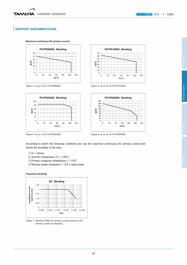
F01P006S05 Derating
F01P025S05 Derating
F01P015S05 Derating
F01P050S05 Derating
Frequency derating
Figure 7: Maximum RMS AC primary current/maximum DC primary current vs frequency
AC Derating
SUPPORT DOCUMENTATION
Maximum continuous DC primary current
Figure 3:Ip vs Ta for F01P006S05
Figure 5:Ip vs Ta for F01P025S05
According to which the following conditions are true the maximum continuous DC primary current plot shows the boundary of the area.
① Ip < Ipmax② Junction temperature Tj < 125℃③ Primary conductor temperature < 110℃④ Resistor power dissipation < 0.5 x rated power
Figure 4:Ip vs Ta for F01P015S05
Figure 6:Ip vs Ta for F01P050S05
CURRENT SENSORS F01P 1 12094/5
Intr
oduc
tion
Flux
gate
sys
tem
O
pen
loop
Cl
osed
loop
37
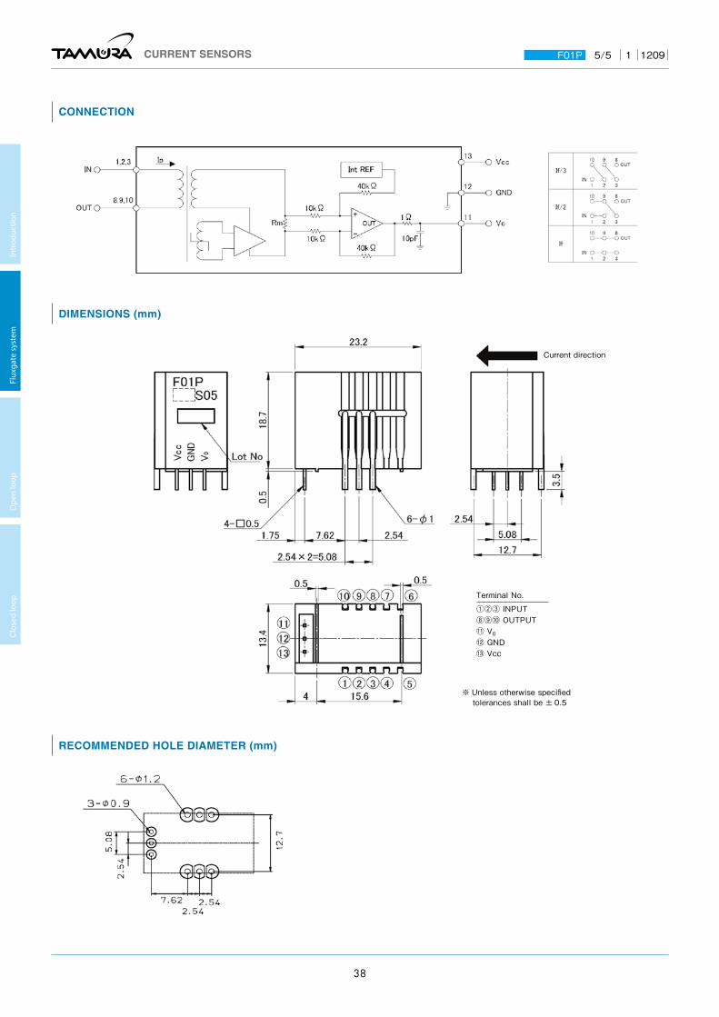
Current direction
DIMENSIONS (mm)
Terminal No.
①②③ INPUT⑧⑨⑩ OUTPUT⑪ V0
⑫ GND⑬ Vcc
※ Unless otherwise specified tolerances shall be ± 0.5
CONNECTION
RECOMMENDED HOLE DIAMETER (mm)
CURRENT SENSORS F01P 1 12095/5
Intr
oduc
tion
Flux
gate
sys
tem
O
pen
loop
Cl
osed
loop
38

F02P SERIES
Fluxgate system / Voltage-output type
ABSOLUTE MAXIMUM RATINGS
Parameters Symbol Unit Value Comment
Supply voltage Vcc V 7
Primary conductor temperature ― ℃ 110
Non repetitive primary current pulse(20µS),in powered or unpowered state.
Îp A 20 × If
ESD(HBM: Human Body Model) ― kV 4 C=100pF,R=1.5kΩ
ENVIRONMENTAL AND MECHANICAL CHARACTERISTICS
Parameters Symbol UnitValue
CommentMIN TYP MAX
Ambient operating temperature Ta ℃ - 40 + 105
Ambient storage temperature TS ℃ - 40 + 105
Mass m g 12
ISOLATION CHARACTERISTICS
Parameters Symbol Unit Value Comment
lnsulation voltage Vd ― AC4100V,for 1minute(Sensing current 0.5mA) Primary ⇔ Secondary
lnsulation Resistance RIS ― ≧ 500MΩ(at DC500V) Primary ⇔ Secondary
Clearance distance dCi ― 7.5mm(TYP) Primary ⇔ Secondary
Creepage distance dCp ― 7.5mm(TYP) Primary ⇔ Secondary
Case material ― ― UL94 V-0
Comparative Tracking Index;(CTI) CTI V 600
Application example ― ― 300V,CAT Ⅲ,PD2 Reinforced isolation,non uniform field according to EN50178,EN61010
― ― 600V,CAT Ⅲ,PD2 Simple isolation,non uniform field according to EN50178,EN61010
RoHS
CURRENT SENSORS F02P 1 12091/6
Intr
oduc
tion
Flux
gate
sys
tem
O
pen
loop
Cl
osed
loop
39

SPECIFICATIONS Ta=+25℃,RL=10kΩ,Vcc=+5V
Parameters Symbol UnitValue
CommentMIN TYP MAX
Rated Current F02P006S05
If A
6
F02P015S05 15
F02P025S05 25
F02P050S05 50
Maximum current(at Vcc= + 5V,Ta= + 105℃)
F02P006S05
Ipmax A
- 20 20
F02P015S05 - 51 51
F02P025S05 - 85 85
F02P050S05 - 150 150
Supply Voltage Vcc V 4.75 5.00 5.25
Number of primary turns Np T 1,2,3
Number of secondary turns F02P006S05
Ns T
1816
F02P015S05 1737
F02P025S05 1764
F02P050S05 1600
Consumption current (at If) F02P006S05
Icc mA
25 Icc = 15 + Ip(mA)/ NsF02P015S05 30
F02P025S05 35
F02P050S05 55
Internal reference voltage(at Ip = 0A) Vref1 V 2.495 2.500 2.505 Ref OUT mode
External reference voltage Vref2 V 0 4 Ref IN mode
Output voltage Vo V 0.375 4.625
Output voltage(at Ip = 0A) Vo V Vref1,Vref2
Electrical offset voltage*1 F02P006S05
Voe mV
- 5.300 5.300
F02P015S05 - 2.210 2.210
F02P025S05 - 1.350 1.350
F02P050S05 - 0.725 0.725
Electrical offset current reffered to primary F02P006S05
Ioe mA
- 51 51
F02P015S05 - 53 53
F02P025S05 - 54 54
F02P050S05 - 58 58
Temperature coefficient of Internal reference voltage TCVref1 ppm/K ± 5.0 ± 50
Temperature coefficient of Output voltage(at Ip = 0A)
F02P006S05
TCVo ppm/K
± 6.0 ± 14 ppm/K of 2.5V(- 40℃~+ 105℃)F02P015S05 ± 2.3 ± 6
F02P025S05 ± 1.4 ± 4
F02P050S05 ± 0.7 ± 3
Sensitivity(Theoretical value) F02P006S05
Gth mV/A
104.2 625mV/IfF02P015S05 41.67
F02P025S05 25
F02P050S05 12.5
Sensitivity error εG % - 0.7 0.7
Temperature coefficient of Sensitivity(at Ta =- 40℃〜+ 105℃) TCG ppm/K ± 40
Output Linearity εL % - 0.1 0.1
Magnetic offset current reffered to primary(at 10×If) IOM A - 0.1 0.1
Output current noise reffered to primary(at 100Hz 〜 100kHz) Ino µA/(Hz)1/2 20 RL = 1kΩ
*1 Offset voltage value is after removal of core hysteresis.
CURRENT SENSORS F02P 1 12092/6
Intr
oduc
tion
Flux
gate
sys
tem
O
pen
loop
Cl
osed
loop
40

STANDARDS
EN50178,EN61010-1,EN60950-1,UL508(file № E243511)※ Please refer to the another sheet about conditions of UL Recognition.
Characteristic curve (TYP)
Figure 1:Linearity curve(Internal reference voltage)
Figure 2: Frequency response curve ex)F02P025S05 Measurement condition Ta=+25℃,RL=1kΩ,Ip=3A,Vcc=+5V
SPECIFICATIONS Ta=+25℃,RL=10kΩ,Vcc=+5V
Parameters Symbol UnitValue
CommentMIN TYP MAX
Peak to peak output ripple at oscillator freqency(f typ = 450kHz)
F02P006S05
― mV
40 160 RL = 1kΩF02P015S05 15 60
F02P025S05 10 40
F02P050S05 5 20
Reaction time(at 10% of If ) F02P006S05
tra µs
0.3 RL = 1kΩ,di/dt = 18A/µs
F02P015S05 0.3 RL = 1kΩ,di/dt = 44A/µs
F02P025S05 0.3 RL = 1kΩ,di/dt = 68A/µs
F02P050S05 0.3 RL = 1kΩ,di/dt = 100A/µs
Response time 1 (at 90% of If ) F02P006S05
tr µs
0.3 RL = 1kΩ,di/dt = 18A/µs
F02P015S05 0.3 RL = 1kΩ,di/dt = 44A/µs
F02P025S05 0.3 RL = 1kΩ,di/dt = 68A/µs
F02P050S05 0.3 RL = 1kΩ,di/dt = 100A/µs
Response time 2 (at 10% of If to 90% of Vo ) tr µs 0.6 RL = 1kΩ,di/dt = If/µs
Frequency bandwidth(± 1dB) BW kHz 200 RL = 1kΩ
Frequency bandwidth(± 3dB) BW kHz 300 RL = 1kΩ
Output Voltage Accuracy(Overall) F02P006S05
XG %
1.7 XG =(100×Voe/625)+εG +εL
F02P015S05 1.2
F02P025S05 1.0
F02P050S05 0.9
CURRENT SENSORS F02P 1 12093/6
Intr
oduc
tion
Flux
gate
sys
tem
O
pen
loop
Cl
osed
loop
41
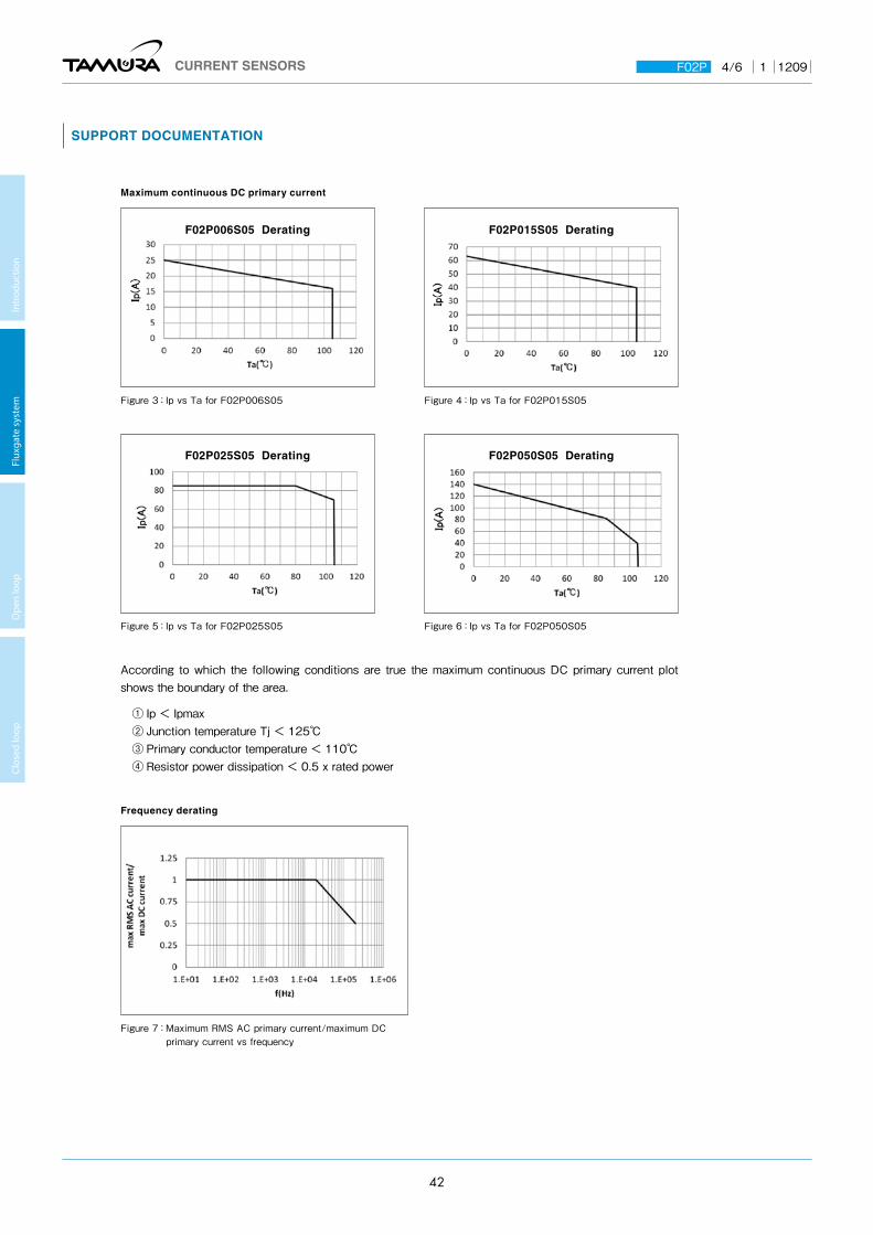
F02P006S05 Derating
F02P025S05 Derating
F02P015S05 Derating
F02P050S05 Derating
SUPPORT DOCUMENTATION
Maximum continuous DC primary current
Figure 3:Ip vs Ta for F02P006S05
Figure 5:Ip vs Ta for F02P025S05
According to which the following conditions are true the maximum continuous DC primary current plot shows the boundary of the area.
① Ip < Ipmax② Junction temperature Tj < 125℃③ Primary conductor temperature < 110℃④ Resistor power dissipation < 0.5 x rated power
Figure 4:Ip vs Ta for F02P015S05
Figure 6:Ip vs Ta for F02P050S05
Frequency derating
Figure 7: Maximum RMS AC primary current/maximum DC primary current vs frequency
CURRENT SENSORS F02P 1 12094/6
Intr
oduc
tion
Flux
gate
sys
tem
O
pen
loop
Cl
osed
loop
42

Reference voltage
The Ref pin has two modes Ref IN and Ref OUT:
< Ref OUT mode >The 2.5V internal precision reference is used by the transducer as the reference point for bipolar measurements;
< Ref IN mode > An external reference voltage is connected to the Ref pin; this voltage is specified in the range 0 to 4 V , its voltage is used as the reference voltage at the time of measurement.
-either to source a typical current of (Vref - 2.5)/680,the maximum value will be 2.2mA typ.when Vref2 = 4V.-or to sink a typical current of (2.5 - Vref2)/680,the maximum value will be 3.68mA typ.when Vref2 = 0V.
The following graphs show how the measuring range of each transducer version depends on external reference voltage value Vref2.
F02P006S05
F02P025S05
F02P015S05
F02P050S05
Upper limit:Ip =- 9.6×Vref2 + 44.4 (Vref2 = 0...4V) Lower limit:Ip =- 9.6×Vref2 + 3.6 (Vref2 = 0...4V)
Upper limit: Ip = 85 (Vref2 = 0...2.5V) Ip =- 40×Vref2 + 185 (Vref2 = 2.5...4V)
Lower limit: Ip =- 40×Vref2 + 15 (Vref2 = 0...2.5V) Ip =- 85 (Vref2 = 2.5...4V)
Upper limit: Ip = 80 (Vref2 = 0...1.29V) Ip =- 24×Vref2 + 111 (Vref2 = 1.29...4V)
Lower limit: Ip =- 24×Vref2 + 9 (Vref2 = 0...3.7V) Ip =- 80 (Vref2 = 3.7...4V)
Upper limit: Ip = 150 (Vref2 = 0...2.75V) Ip =- 80×Vref2 + 370 (Vref2 = 2.75...4V)
Lower limit: Ip =- 80×Vref2 + 30 (Vref2 = 0...2.25V) Ip =- 150 (Vref2 = 2.25...4V)
If you do not want to use the Ref pin, please unconnected.
CURRENT SENSORS F02P 1 12095/6
Intr
oduc
tion
Flux
gate
sys
tem
O
pen
loop
Cl
osed
loop
43

CONNECTION
RECOMMENDED HOLE DIAMETER (mm)
Current direction
DIMENSIONS (mm)
Terminal No.
①②③ INPUT⑧⑨⑩ OUTPUT⑪ Vref⑫ V0
⑬ GND⑭ Vcc
※ Unless otherwise specified tolerances shall be ± 0.5
CURRENT SENSORS F02P 1 12096/6
Intr
oduc
tion
Flux
gate
sys
tem
O
pen
loop
Cl
osed
loop
44
F03P SERIES
Fluxgate system / Voltage-output type
ABSOLUTE MAXIMUM RATINGS
Parameters Symbol Unit Value Comment
Supply voltage Vcc V 7
Primary conductor temperature ― ℃ 110
Non repetitive primary current pulse(20µS),in powered or unpowered state.
Îp A 20 × If
ESD(HBM: Human Body Model) ― kV 4 C=100pF,R=1.5kΩ
ENVIRONMENTAL AND MECHANICAL CHARACTERISTICS
Parameters Symbol UnitValue
CommentMIN TYP MAX
Ambient operating temperature Ta ℃ - 40 + 105
Ambient storage temperature TS ℃ - 40 + 105
Mass m g 12
ISOLATION CHARACTERISTICS
Parameters Symbol Unit Value Comment
lnsulation voltage Vd ― AC4300V,for 1minute(Sensing current 0.5mA) Primary ⇔ Secondary
lnsulation Resistance RIS ― ≧ 500MΩ(at DC500V) Primary ⇔ Secondary
Clearance distance dCi ― 8.2mm(TYP) Primary ⇔ Secondary
Creepage distance dCp ― 8.2mm(TYP) Primary ⇔ Secondary
Case material ― ― UL94 V-0
Comparative Tracking Index;(CTI) CTI V 600
Application example ― ― 300V,CAT Ⅲ,PD2 Reinforced isolation, non uniform field according to EN61010
― ― 600V,CAT Ⅲ,PD2 Reinforced isolation, non uniform field according to EN50178
― ― 1000V,CAT Ⅲ,PD2 Simple isolation, non uniform field according to EN50178
RoHS
CURRENT SENSORS F03P 1 12091/6
Intr
oduc
tion
Flux
gate
sys
tem
O
pen
loop
Cl
osed
loop
45

SPECIFICATIONS Ta=+25℃,Np=1T,RL=10kΩ,Vcc=+5V
Parameters Symbol UnitValue
CommentMIN TYP MAX
Rated Current F03P006S05
If A
6
F03P015S05 15
F03P025S05 25
F03P050S05 50
Maximum current F03P006S05
Ipmax A
- 20 20
F03P015S05 - 51 51
F03P025S05 - 85 85
F03P050S05 - 150 150
Supply Voltage Vcc V 4.75 5.00 5.25
Number of primary turns Np T 1,2,3,4
Number of secondary turns F03P006S05
Ns T
1816
F03P015S05 1737
F03P025S05 1764
F03P050S05 1600
Consumption current (at If) F03P006S05
Icc mA
25 Icc=15+Ip(mA)/NsF03P015S05 30
F03P025S05 35
F03P050S05 55
Internal reference voltage(at Ip=0A) Vref1 V 2.495 2.500 2.505 Ref OUT mode
External reference voltage Vref2 V 0 4 Ref IN mode
Output voltage Vo V 0.375 4.625
Output voltage(at Ip=0A) Vo V Vref1,Vref2
Electrical offset voltage*1 F03P006S05
Voe mV
- 5.300 5.300
F03P015S05 - 2.210 2.210
F03P025S05 - 1.350 1.350
F03P050S05 - 0.725 0.725
Electrical offset current reffered to primary F03P006S05
Ioe mA
- 51 51
F03P015S05 - 53 53
F03P025S05 - 54 54
F03P050S05 - 58 58
Temperature coefficient of Internal reference voltage TCVref1 ppm/K ± 5.0 ± 50
Temperature coefficient of Output voltage (at Ip=0A)
F03P006S05
TCVo ppm/K
± 6.0 ± 14 ppm/K of 2.5V(- 40℃~+ 105℃)F03P015S05 ± 2.3 ± 6
F03P025S05 ± 1.4 ± 4
F03P050S05 ± 0.7 ± 3
Sensitivity(Theoretical value) F03P006S05
Gth mV/A
104.2 625mV/IfF03P015S05 41.67
F03P025S05 25
F03P050S05 12.5
Sensitivity error εG % - 0.7 0.7
Temperature coefficient of Sensitivity(at Ta= - 40℃〜+ 105℃) TCG ppm/K ± 40
Output Linearity(at If) εL % - 0.1 0.1
Magnetic offset current reffered to primary(at 10×If) IOM A - 0.1 0.1
Output current noise reffered to primary(at 100Hz 〜 100kHz) Ino µA/(Hz)1/2 20 RL=1kΩ
*1 Offset voltage value is after removal of core hysteresis.
CURRENT SENSORS F03P 1 12092/6
Intr
oduc
tion
Flux
gate
sys
tem
O
pen
loop
Cl
osed
loop
46

STANDARDS
EN50178,EN61010-1,EN60950-1,UL508(file № E243511)※ Please refer to the another sheet about conditions of UL Recognition.
Figure 2: Frequency response curve ex)F03P025S05L Measurement condition Ta=+25℃,RL=1kΩ,Ip=3A,Vcc=+5V
SPECIFICATIONS Ta=+25℃,Np=1T,RL=10kΩ,Vcc=+5V
Parameters Symbol UnitValue
CommentMIN TYP MAX
Peak to peak output ripple at oscillator freqency(f typ=450kHz)
F03P006S05
― mV
40 160 RL=1kΩ
F03P015S05 15 60
F03P025S05 10 40
F03P050S05 5 20
Reaction time(at 10% of If ) F03P006S05
tra µs
0.3 RL=1kΩ,di/dt=18A/µs
F03P015S05 0.3 RL=1kΩ,di/dt=44A/µs
F03P025S05 0.3 RL=1kΩ,di/dt=68A/µs
F03P050S05 0.3 RL=1kΩ,di/dt=100A/µs
Response time 1 (at 90% of If ) F03P006S05
tr µs
0.3 RL=1kΩ,di/dt=18A/µs
F03P015S05 0.3 RL=1kΩ,di/dt=44A/µs
F03P025S05 0.3 RL=1kΩ,di/dt=68A/µs
F03P050S05 0.3 RL=1kΩ,di/dt=100A/µs
Response time 2 (at 10% of If to 90% of Vo ) tr µs 0.6 RL=1kΩ,di/dt=If/µs
Frequency bandwidth(± 1dB) BW kHz 200 RL=1kΩ
Frequency bandwidth(± 3dB) BW kHz 300 RL=1kΩ
Output Voltage Accuracy(Overall) F03P006S05
XG %
1.7 XG=(100×Voe/625)+εG+εL
F03P015S05 1.2
F03P025S05 1.0
F03P050S05 0.9
Characteristic curve (TYP)
Figure 1:Linearity curve(Internal reference voltage)
CURRENT SENSORS F03P 1 12093/6
Intr
oduc
tion
Flux
gate
sys
tem
O
pen
loop
Cl
osed
loop
47

F03P006S05 Derating
F03P025S05 Derating
F03P015S05 Derating
F03P050S05 Derating
SUPPORT DOCUMENTATION
Maximum continuous DC primary current
Figure 3:Ip vs Ta for F03P006S05
Figure 5:Ip vs Ta for F03P025S05
According to which the following conditions are true the maximum continuous DC primary current plot shows the boundary of the area.
① Ip < Ipmax② Junction temperature Tj < 125℃③ Primary conductor temperature < 110℃④ Resistor power dissipation < 0.5 x rated power
Figure 4:Ip vs Ta for F03P015S05
Figure 6:Ip vs Ta for F03P050S05
Frequency derating
Figure 7: Maximum RMS AC primary current/maximum DC primary current vs frequency
AC Derating
CURRENT SENSORS F03P 1 12094/6
Intr
oduc
tion
Flux
gate
sys
tem
O
pen
loop
Cl
osed
loop
48

Reference voltage
The Ref pin has two modes Ref IN and Ref OUT:
< Ref OUT mode >The 2.5V internal precision reference is used by the transducer as the reference point for bipolar measurements;
< Ref IN mode > An external reference voltage is connected to the Ref pin; this voltage is specified in the range 0 to 4 V, its voltage is used as the reference voltage at the time of measurement.
-either to source a typical current of (Vref - 2.5)/680,the maximum value will be 2.2mA typ.when Vref2 = 4V.-or to sink a typical current of (2.5 - Vref2)/680,the maximum value will be 3.68mA typ.when Vref2 = 0V.
The following graphs show how the measuring range of each transducer version depends on external reference voltage value Vref2.
F03P006S05
F03P025S05
F03P015S05
F03P050S05
Upper limit:Ip =- 9.6×Vref2 + 44.4 (Vref2 = 0...4V) Lower limit:Ip =- 9.6×Vref2 + 3.6 (Vref2 = 0...4V)
Upper limit: Ip = 85 (Vref2 = 0...2.5V) Ip =- 40×Vref2 + 185 (Vref2 = 2.5...4V)
Lower limit: Ip =- 40×Vref2 + 15 (Vref2 = 0...2.5V) Ip =- 85 (Vref2 = 2.5...4V)
Upper limit: Ip = 80 (Vref2 = 0...1.29V) Ip =- 24×Vref2 + 111 (Vref2 = 1.29...4V)
Lower limit: Ip =- 24×Vref2 + 9 (Vref2 = 0...3.7V) Ip =- 80 (Vref2 = 3.7...4V)
Upper limit: Ip = 150 (Vref2 = 0...2.75V) Ip =- 80×Vref2 + 370 (Vref2 = 2.75...4V)
Lower limit: Ip =- 80×Vref2 + 30 (Vref2 = 0...2.25V) Ip =- 150 (Vref2 = 2.25...4V)
If you do not want to use the Ref pin, please unconnected.
CURRENT SENSORS F03P 1 12095/6
Intr
oduc
tion
Flux
gate
sys
tem
O
pen
loop
Cl
osed
loop
49

CONNECTION
RECOMMENDED HOLE DIAMETER (mm)
DIMENSIONS (mm)
Terminal number
②③④⑤ Input ⑥⑦⑧⑨ Output⑪ Vref⑫ Vo⑬ GND⑭ Vcc
※ Unless otherwise specified, tolerances shall be ± 0.5mm
Current direction
CURRENT SENSORS F03P 1 12096/6
Intr
oduc
tion
Flux
gate
sys
tem
O
pen
loop
Cl
osed
loop
50

F23PxxxS05R SERIES
Fluxgate system / Voltage-output type
ABSOLUTE MAXIMUM RATINGS
Parameters Symbol Unit Value Comment
Supply voltage Vcc V 7
Primary conductor temperature ― ℃ 110
ESD(HBM: Human Body Model) ― kV 4 C=150pF,R=330Ω
ENVIRONMENTAL AND MECHANICAL CHARACTERISTICS
Parameters Symbol UnitValue
CommentMIN TYP MAX
Ambient operating temperature Ta ℃ - 40 + 85
Ambient storage temperature TS ℃ - 40 + 85
Mass m g 13
ISOLATION CHARACTERISTICS
Parameters Symbol Unit Value Comment
lnsulation voltage Vd ― AC5000V,for 1minute(Sensing current 0.5mA) Primary ⇔ Secondary
lnsulation Resistance RIS ― ≧ 500MΩ(at DC500V) Primary ⇔ Secondary
Clearance distance dCi ― 11.0mm(MIN) Primary ⇔ Secondary
Creepage distance dCp ― 12.7mm(MIN) Primary ⇔ Secondary
Case material ― ― UL94 V-0
Comparative Tracking Index;(CTI) CTI V 600
Application example― ― 600V,CAT Ⅲ,PD2
Reinforced isolation,non uniform field according to EN50178,IEC61800-5-1
― ― 1000V,CAT Ⅲ,PD2Basic isolation,non uniform field according to EN50178,IEC61800-5-1
RoHS
CURRENT SENSORS F23P 1 17031/6
Intr
oduc
tion
Flux
gate
sys
tem
O
pen
loop
Cl
osed
loop
51

SPECIFICATIONS Ta=+25℃,Np=1T,RL=10kΩ,Vcc=+5V
Parameters Symbol UnitValue
CommentMIN TYP MAX
Rated Current F23P050S05RIf A
50
F23P100S05R 100
Maximum current(at Vcc= + 5V,Ta= + 85℃) F23P050S05RIpmax A
- 150 + 150
F23P100S05R - 200 + 200
Supply Voltage Vcc V 4.75 5.00 5.25
Number of primary turns Np T 1,2,3
Number of secondary turns F23P050S05RNs T
1441
F23P100S05R 1127
Consumption current (at If) F23P050S05RIcc mA
55 Icc=20+If/NsF23P100S05R 110
Internal reference voltage(at Ip=0A) Vref1 V 2.495 2.500 2.505 Ref OUT mode
External reference voltage Vref2 V 0 4 Ref IN mode
Output voltage(at Ip=0A) Vo V Vref1,Vref2
Electrical offset voltage*1 F23P050S05RVoe mV - 2.5 2.5
F23P100S05R
Electrical offset current reffered to primary F23P050S05RIoe mA
- 200 200
F23P100S05R - 400 400
Temperature coefficient of Internal reference voltage TCVref1 ppm/K ± 5.0 ± 50
Temperature coefficient of Output voltage (at Ip=0A)
F23P050S05RTCVo ppm/K ± 3.0 ± 10 ppm/K of 2.5V
(- 40℃~+ 85℃)F23P100S05R
Sensitivity(Theoretical value) F23P050S05RGth mV/A
12.5 625mV(at If)= | Vref - Vout |/IfF23P100S05R 6.25
Sensitivity error εG % - 0.7 0.7
Temperature coefficient of Sensitivity(at Ta= - 40℃〜+ 85℃) TCG ppm/K ± 40
Output Linearity(at If) εL % - 0.1 0.1
External recommended resistance of Vout RL kΩ 10
External recommended capacitance of Vout CL pF 500
*1 Offset voltage value is after removal of core hysteresis.
CURRENT SENSORS F23P 1 17032/6
Intr
oduc
tion
Flux
gate
sys
tem
O
pen
loop
Cl
osed
loop
52
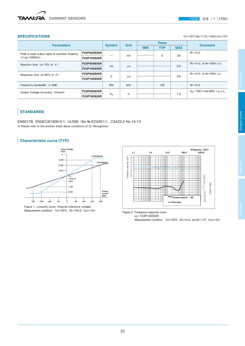
STANDARDS
EN50178,EN(IEC)61800-5-1,UL508(file № E243511),CSA22.2 No.14-13※ Please refer to the another sheet about conditions of UL Recognition.
Figure 2: Frequency response curve ex)F23P100S05R Measurement condition Ta=+25℃,RL=1kΩ,Ip=3A×3T,Vcc=+5V
SPECIFICATIONS Ta=+25℃,Np=1T,RL=10kΩ,Vcc=+5V
Parameters Symbol UnitValue
CommentMIN TYP MAX
Peak to peak output ripple at oscillator freqency(f typ=450kHz)
F23P050S05R― mV 5 20
RL=1kΩ
F23P100S05R
Reaction time(at 10% of If ) F23P050S05Rtra µs 0.5
RL=1kΩ,di/dt=100A/µs
F23P100S05R
Response time (at 90% of If ) F23P050S05Rtr µs 0.5
RL=1kΩ,di/dt=100A/µs
F23P100S05R
Frequency bandwidth(± 3dB) BW kHz 100 RL=1kΩ
Output Voltage Accuracy(Overall) F23P050S05RXG % 1.2
XG=(100×Voe/625)+εG+εL
F23P100S05R
Characteristic curve (TYP)
Figure 1:Linearity curve(Internal reference voltage) Measurement condition Ta=+25℃,RL=10kΩ,Vcc=+5V
CURRENT SENSORS F23P 1 17033/6
Intr
oduc
tion
Flux
gate
sys
tem
O
pen
loop
Cl
osed
loop
53
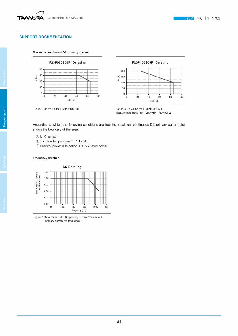
F23P050S05R Derating F23P100S05R Derating
SUPPORT DOCUMENTATION
Maximum continuous DC primary current
Figure 3:Ip vs Ta for F23P050S05R
According to which the following conditions are true the maximum continuous DC primary current plot shows the boundary of the area.
① Ip < Ipmax② Junction temperature Tj < 125℃③ Resistor power dissipation < 0.5 x rated power
Figure 4:Ip vs Ta for F23P100S05RMeasurement condition Vcc=+5V , RL=10kΩ
Frequency derating
Figure 7: Maximum RMS AC primary current/maximum DC primary current vs frequency
AC Derating
CURRENT SENSORS F23P 1 17034/6
Intr
oduc
tion
Flux
gate
sys
tem
O
pen
loop
Cl
osed
loop
54

Reference voltage
The Ref pin has two modes Ref IN and Ref OUT:
< Ref OUT mode >The 2.5V internal precision reference is used by the transducer as the reference point for bipolar measurements;
< Ref IN mode > An external reference voltage is connected to the Ref pin; this voltage is specified in the range 0 to 4 V , its voltage is used as the reference voltage at the time of measurement.
-either to source a typical current of (Vref - 2.5)/680,the maximum value will be 2.2mA typ.when Vref2 = 4V.-or to sink a typical current of (2.5 - Vref2)/680,the maximum value will be 3.68mA typ.when Vref2 = 0V.
The following graphs show how the measuring range of each transducer version depends on external reference voltage value Vref2.
F23P050S05R F23P100S05R
Upper limit: Ip = 150 (Vref2 = 0...2.5V) Ip =- 80×Vref2 + 350 (Vref2 = 2.5...4V)
Lower limit: Ip =- 80×Vref2 + 50 (Vref2 = 0...2.5V) Ip =- 150 (Vref2 = 2.5...4V)
Upper limit: Ip = 200 (Vref2 = 0...2.5V) Ip =- 160×Vref2 + 600 (Vref2 = 2.5...4V)
Lower limit: Ip =- 160×Vref2 + 200 (Vref2 = 0...2.5V) Ip =- 200 (Vref2 = 2.5...4V)
If you do not want to use the Ref pin, please unconnected.
CONNECTION
CURRENT SENSORS F23P 1 17035/6
Intr
oduc
tion
Flux
gate
sys
tem
O
pen
loop
Cl
osed
loop
55

RECOMMENDED HOLE DIAMETER (mm)
DIMENSIONS (mm)
Terminal No.
① Primary input current 1(+)② Primary input current 2(+)③ Primary input current 3(+)④Primary input current 3(-)⑤Primary input current 2(-)⑥Primary input current 1(-)⑦ Vout⑧ Vcc(+5V)⑨ GND⑩ Vref(IN/OUT)
※ Tolerance: ± 0.2 Unit: mm
Current direction
CURRENT SENSORS F23P 1 17036/6
Intr
oduc
tion
Flux
gate
sys
tem
O
pen
loop
Cl
osed
loop
56
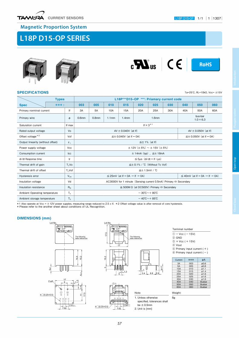
L18P∗∗∗D15-OP
5±1
4±0.
5
14.4
15.2
+–
2-φA
17.5
1.5
±0.3
617
1
3.75
11
2.547.62
L18P∗∗∗D15-OP
5 5.4 8.8 2.8
2.54±0.3
7.62
3
1.3
15.2
1 4±0.
5
+
–
4-□(0.25×0.5)
Current ∗∗∗ φA3A5A10A15A20A25A30A
φ0.6φ0.8φ1.1φ1.4φ1.6φ1.6φ1.6
003005010015020025030
40A Busbar04050A Busbar05060A Busbar060
Lot No. Lot No.
The following, table references
The following, table references
17
17.5
③④
⑤⑥
①② ③④
⑤
⑥
①②
4-□(0.25×0.5)
Current ∗∗∗ φA3A5A10A15A20A25A30A
φ0.6φ0.8φ1.1φ1.4φ1.6φ1.6φ1.6
003005010015020025030
40A Busbar04050A Busbar05060A Busbar060
SPECIFICATIONS Ta=25˚C, RL=10kΩ, Vcc= ±15V
Spec
Types L18P***D15–OP ***: Priamary current code
*** : 003 005 010 015 020 025 030 040 050 060
Primary norminal current If 3A 5A 10A 15A 20A 25A 30A 40A 50A 60A
Primary wire φ 0.6mm 0.8mm 1.1mm 1.4mm 1.6mm bus-bar1.0×6.3
Saturation current If max If×3*1
Rated output voltage Vo 4V ± 0.040V (at If) 4V ± 0.050V (at If)
Offset voltage*2 Vof ≦± 0.040V (at If = 0A) ≦± 0.050V (at If = 0A)
Output linearity (without offset) εL ≦± 1%(at If)
Power supply voltage Vcc ± 12V (± 5%) ~ ± 15V (± 5%)
Consumption current Icc ± 14mA (typ), ≦± 18mA
di/dt Response time tr ≦ 5μs(di/dt = If /μs)
Thermal drift of gain TCVo ≦± 0.1% / ℃(Without Tc Vof)
Thermal drift of offset TCVof ≦± 1.5mV / ℃
Hysteresis error VOH ≦ 25mV (at If = 0A → If → 0A) ≦ 40mV (at If = 0A → If → 0A)
Insulation voltage Vd AC3000V for 1 minute(Sensing current 0.5mA) Primary ⇔ Secondary
Insulation resistance RIS ≧ 500MΩ (at DC500V) Primary ⇔ Secondary
Ambient Operating temperature TA ー 30℃〜+ 80℃
Ambient storage temperature TS ー 40℃〜+ 85℃
*1 Also operate at Vcc = ±12V power supples, measuring range reduced to 2.5 x If. *2 Offset voltage value is after removal of core hysteresis.* Please refer to the another sheet about conditions of UL Recognition.
L18P D15-OP SERIES
Magnetic Proportion System
L18P D15-OP 1 13071/1
DIMENSIONS (mm)
RoHS
Terminal number
① - Vcc ( ー 15V)② GND③ + Vcc ( + 15V)④ Vout⑤ Primary input current ( + )⑥ Primary input current ( ー )
Weight:
8g
Note
1. Unless otherwise specified, tolerances shall be ± 0.5mm
2. Unit is [mm]
CURRENT SENSORS
Intr
oduc
tion
Flux
gate
sys
tem
O
pen
loop
Cl
osed
loop
57

SL18P D15 SERIES
Magnetic Proportion System
SL18P∗∗∗D15
5±1
4±0.
5
14.4
15.2
+–
2-φA
17.5
1.5
±0.3
617
1
3.75
11
2.547.62
SL18P∗∗∗D15
5 5.4 8.8 2.8
2.54±0.3
7.62
3
1.3
15.2
1 4±0.
5
+
–
4-□(0.25×0.5)
Current ∗∗∗ φA3A5A10A15A20A25A30A
φ0.6φ0.8φ1.1φ1.4φ1.6φ1.6φ1.6
003005010015020025030
40A Busbar04050A Busbar05060A Busbar060
Lot No. Lot No.
(The following, table references)
(The following, table references)
17
17.5
③④
⑤⑥
①② ③④
⑤
⑥
①②
4-□(0.25×0.5)
DIMENSIONS
SPECIFICATIONS Ta=25˚C, RL=10kΩ, Vcc=±15V
Spec
Types SL18P***D15***: Priamary current code
*** : 003 005 010 015 020 025 030 040 050 060
Primary norminal current If 3A 5A 10A 15A 20A 25A 30A 40A 50A 60A
Primary wire φ 0.6mm 0.8mm 1.1mm 1.4mm 1.6mm bus-bar1.0×6.3
Saturation current If max If×3*1
Rated output voltage Vo 4V ± 0.040V(at If) 4V ± 0.050V(at If)
Offset voltage*2 Vof ≦± 0.040V(at If = 0A) ≦± 0.050V(at If = 0A)
Output linearity(without offset) εL ≦± 1%(at If)
Power supply voltage Vcc ± 12V(± 5%) ~ ± 15V(± 5%)
Consumption current Icc ± 12mA (typ), ≦ 15mA
di/dt Response time tr ≦ 5µs(di/dt = If /µs)
Thermal drift of gain TCVo ≦± 0.1% / ℃(Without Tc Vof)
Thermal drift of offset TCVof ≦± 1.5mV / ℃
Hysteresis error VOH ≦ 25mV(at If = 0A → If → 0A) ≦ 40mV(at If = 0A → If → 0A)
Insulation voltage Vd AC3000V for 1 minute(Sensing current 0.5mA)Primary ⇔ Secondary
Insulation resistance RIS ≧ 500MΩ (at DC500V)Primary ⇔ Secondary
Ambient Operating temperature TA ー 30℃~+ 80℃
Ambient storage temperature TS ー 40℃~+ 85℃
*1 Also operate at Vcc = ± 12V power supples, measuring range reduced to 2.5 x If. *2 Offset voltage value is after removal of core hysteresis. *Please refer to the another sheet about conditions of UL Recognition. *Anti-Sulfurated (Used resistors : Gold internal Electrodes, PCB coating : HumiSeal®) *Reliability test High Temperature and High Humidity Operation Test (85℃ , 85%RH, 1000h, N=11, Pass)
RoHS Anti-Sulfuratad
Terminal number
① - Vcc ( ー 15V)② GND③ + Vcc ( + 15V)④ Vout⑤ Primary input current ( + )⑥ Primary input current ( ー )
Weight:
8g
Note
1. Unless otherwise specified, tolerances shall be ± 0.5mm
2. Unit is [mm]
CURRENT SENSORS SL18P D15 1 13071/1
Intr
oduc
tion
Flux
gate
sys
tem
O
pen
loop
Cl
osed
loop
58

L18P D15 SERIES
Magnetic Proportion System
RoHS
TAMURA recommends L18P D15-OP seriesas a succession model.
Current ***40A 04050A 05060A 060
5 5.4 8.8 2.8
2.54±0.3
7.62
3
1.3
15.2
The following, table references
Lot No.
* * *
17
17.5
1 4±0.
5
+
-
4
5
6
123
4-□(0.25×0.5)
SPECIFICATIONS Ta=25˚C, RL=10kΩ, Vcc=±15V
TypesSpec
L18P003D15 L18P005D15 L18P010D15 L18P015D15 L18P020D15 L18P025D15 L18P030D15 L18P040D15 L18P050D15 L18P060D15
Primary norminal current If 3A 5A 10A 15A 20A 25A 30A 40A 50A 60A
Primary wire φ 0.6mm 0.8mm 1.1mm 1.4mm 1.6mm bus-bar1.0×6.3
Saturation current If max If×3
Rated output voltage Vo 4V ± 0.040V(at If) 4V ± 0.050V(at If)
Offset voltage Vof ≦± 0.040V (at If = 0A)*1 ≦± 0.050V(at If = 0A)*1
Output linearity (without offset) εL ≦± 1%(at If)
Power supply voltage Vcc ± 15V ± 5%
Consumption current Icc ± 12mA (typ), ≦± 15mA
di/dt Response time tr ≦ 5µs(di/dt = If /µs)
Thermal drift of gain TCVo ≦± 0.1% / ℃(Without Tc Vof)
Thermal drift of offset TCVof ≦± 1.5mV / ℃
Hysteresis error VOH ≦ 25mV(at If = 0A → If → 0A) ≦ 40mV(at If = 0A → If → 0A)
Insulation voltage Vd AC3000V for 1 minute(Sensing current 0.5mA)Primary ⇔ Secondary
Insulation resistance RIS ≧ 500MΩ (at DC500V) Primary ⇔ Secondary
Ambient Operating temperature TA ー 30℃~+ 80℃
Ambient storage temperature TS ー 40℃~+ 85℃
*1 Offset voltage value is after removal of core hysteresis. Please refer to the another sheet about conditions of UL Recognition.
DIMENSIONS (mm)
Current *** φA3A5A10A15A20A25A30A
φ0.6φ0.8φ1.1φ1.4φ1.6φ1.6φ1.6
003005010015020025030
±15
4±0.5
14.4
15.2
6 5+-
3 24
4-□(0.25×0.5)
2-φA
1
17.5
1.5
±0.3
617
1
3.75
11
2.547.62
* * *
The following, table references
Lot No.
Terminal number
1 - Vcc2 GND3 + Vcc4 OUT5 + IN6 - IN
Note
1. Unless otherwise specified, tolerances shall be ±0.5mm
2. Unit is [mm]
Terminal number
1 - Vcc2 GND3 + Vcc4 OUT5 + IN6 - IN
Note
1. Unless otherwise specified, tolerances shall be ±0.5mm
2. Unit is [mm]
CURRENT SENSORS L18P D15 4 13071/1
Intr
oduc
tion
Flux
gate
sys
tem
O
pen
loop
Cl
osed
loop
59

Current *** φAφ0.6φ0.8φ1.1φ1.4φ1.6φ1.6φ1.6
003005010015020025030
3A5A10A15A20A25A30A
4±0.
5
5±1
14.4
15.2
+-
3 24
4-□(0.25×0.5)
2-φA
1
17.5
1.5
6
±0.3
171
3.75
11
2.547.62
6 5
The following, table references
Lot No.
* * *
Current ***40A 04050A 05060A 060
5 5.4 8.8 2.8
2.54 ±0.3
7.62
3
1.3
15.2
The following, table references
Lot No.
* * *
17
17.5
1 4±0.5
+
-
5
6
12344-□(0.25×0.5)
SPECIFICATIONS Ta=25˚C, RL=10kΩ, Vcc= +5V
TypesSpec L18P003S05 L18P005S05 L18P010S05 L18P015S05 L18P020S05 L18P025S05 L18P030S05 L18P040S05 L18P050S05 L18P060S05
Primary norminal current If 3A 5A 10A 15A 20A 25A 30A 40A 50A 60A
Primary wire φ 0.6mm 0.8mm 1.1mm 1.4mm 1.6mm bus-bar1.0×6.3
Saturation current If max If×1.5*1
Rated output voltage Vo Vof + 1.5V ± 0.045V (at If)
Offset voltage Vof Vcc/2 ± 0.035V (at If = 0A)*2
Output linearity (without offset) εL ≦± 1%(at If)
Power supply voltage Vcc + 5V ± 5%
Consumption current Icc ≦ 15mA
di/dt Response time tr ≦ 5µs(di/dt = If /µs)
Thermal drift of gain TCVo ≦± 2.0mV / ℃(Without Tc Vof)
Thermal drift of offset TCVof ≦± 2.0mV / ℃
Hysteresis error VOH ≦ 25mV (at If = 0A → If → 0A)
Insulation voltage Vd AC3000V for 1 minute(Sensing current 0.5mA) Primary ⇔ Sacondary
Insulation resistance RIS ≧ 500MΩ (at DC500V) Primary ⇔ Sacondary
Ambient Operating temperature TA ー 30℃~+ 80℃
Ambient storage temperature TS ー 40℃~+ 85℃
*1 Vcc= + 5.0V (depending on Vcc) *2 Offset voltage value is after removal of core hysteresis. Please refer to the another sheet about conditions of UL Recognition.
DIMENSIONS (mm)
L18P S05 SERIES
Magnetic Proportion System
L18P S05 4 12091/1
Terminal number
1. GND2. GND3. + Vcc4. OUT5. + IN6. - IN
Note
1. Unless otherwise specified, tolerances shall be ±0.5mm
2. Unit is [mm]
RoHS
Terminal number
1. GND2. GND3. + Vcc4. OUT5. + IN6. - IN
Note
1. Unless otherwise specified, tolerances shall be ± 0.5mm
2. Unit is [mm]
CURRENT SENSORS
Intr
oduc
tion
Flux
gate
sys
tem
O
pen
loop
Cl
osed
loop
60

SPECIFICATIONS Ta=25˚C, RL=10kΩ, Vcc= +5V
TypesSpec
L18P003S05R
L18P005S05R
L18P010S05R
L18P015S05R
L18P020S05R
L18P025S05R
L18P030S05R
L18P040S05R
L18P050S05R
L18P060S05R
Primary norminal current If 3A 5A 10A 15A 20A 25A 30A 40A 50A 60A
Primary wire φ 0.6mm 0.8mm 1.1mm 1.4mm 1.6mm bus-bar 1.0×6.3
Saturation current If max If×3
Rated output voltage Vo Vof + 0.625V ± 0.045V(at If)
Offset voltage Vof 2.5V ± 0.035V(at If = 0A)*1
Output linearity (without offset) εL ≦± 1%(at If)
Power supply voltage Vcc + 5V ± 5%
Consumption current Icc ≦ 15mA
di / dt Response time tr ≦ 5μs(di/dt = If /μs)
Thermal drift of gain TCVo ≦± 0.1% / ℃(Without Tc Vof)
Thermal drift of offset TCVof ≦± 1.0mV / ℃
Hysteresis error VOH ≦ 25mV (at If = 0A → If → 0A)
Insulation voltage Vd AC3000V for 1 minute(Sensing current 0.5mA) Primary ⇔ Sacondary
Insulation resistance RIS ≧ 500MΩ (at DC500V) Primary ⇔ Sacondary
Ambient Operating temperature TA ー30℃〜+ 80℃
Ambient storage temperature TS ー 40℃〜+ 85℃
*1 Offset voltage value is after removal of core hysteresis. Please refer to the another sheet about conditions of UL Recognition.
L18P S05R SERIES
Magnetic Proportion System
L18P S05R 3 12031/1
Current φA***φ0.6φ0.8φ1.1φ1.4φ1.6φ1.6φ1.6
003005010015020025030
3A5A10A15A20A25A30A
4±0.5
5±1
14.4
15.2
+-5
2 1
4-□(0.25×0.5)
4 3
2-φA
6
6
±0.3
171
3.75
11
1.5
17.5
2.547.62
The following, table references
Lot No.
* * *
Current ***40A 04050A 05060A 060
2.54±0.3
7.62
5.4 8.8 2.85
+
- 6
1234
5
4-□(0.25×0.5)
The following, table references
Lot No.
* * *
17
17.5
1 4±0.53
1.3
15.2
DIMENSIONS (mm)
Terminal number
1. GND2. GND 3. + Vcc4. OUT5. + IN6. - IN
Terminal number
1. GND2. GND 3. + Vcc4. OUT5. + IN6. - IN
Note
1. Unless otherwise specified, tolerances shall be ± 0.5mm
2. Unit is [mm]
Note
1. Unless otherwise specified, tolerances shall be ± 0.5mm
2. Unit is [mm]
RoHS
CURRENT SENSORS
Intr
oduc
tion
Flux
gate
sys
tem
O
pen
loop
Cl
osed
loop
61
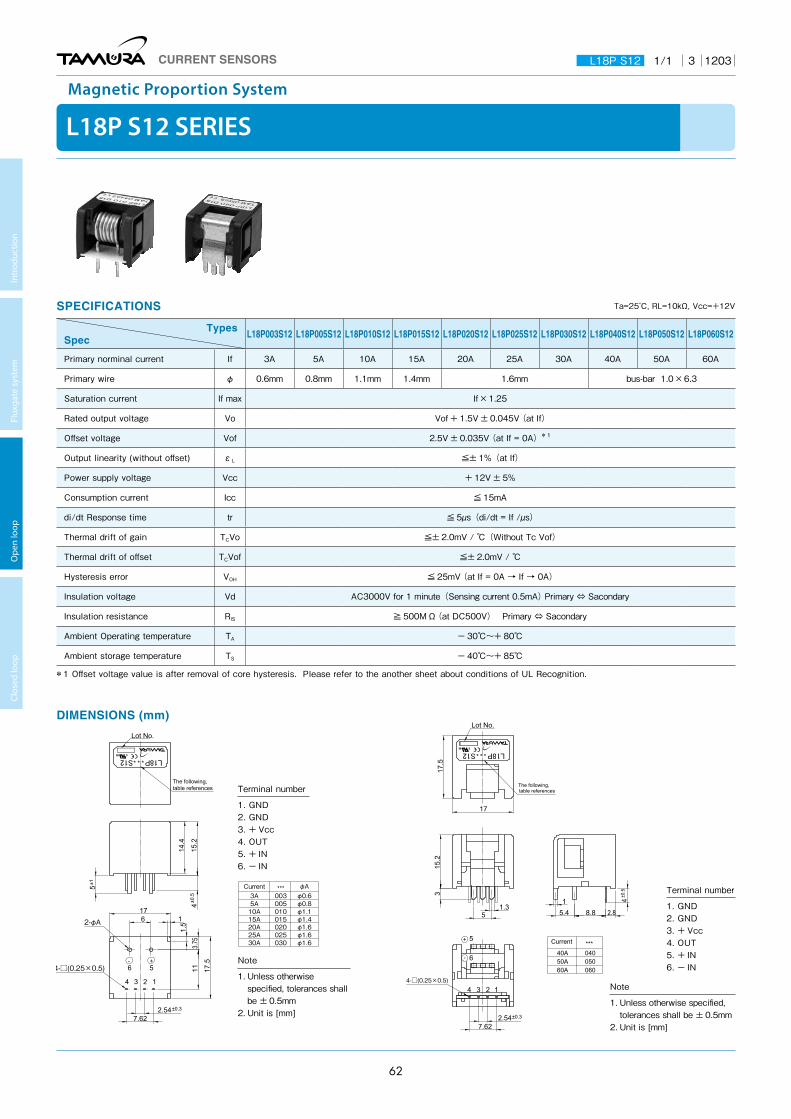
Current *** φAφ0.6φ0.8φ1.1φ1.4φ1.6φ1.6φ1.6
003005010015020025030
3A5A10A15A20A25A30A
4±0.5
5±1
+-6
2 1
4-□(0.25×0.5)
4
2-φA
5
6
±0.3
171
3.75
111.
5
17.5
2.547.62
14.4
15.2
The following, table references
Lot No.
* * *
3
Current ***40A 04050A 05060A 060
5 5.4 8.8 2.8
2.54±0.3
7.62
3
1.3
15.2
1 4±0.5
The following, table references
Lot No.
* * *
17
17.5
+
- 6
1234
5
4-□(0.25×0.5)
SPECIFICATIONS Ta=25˚C, RL=10kΩ, Vcc=+12V
TypesSpec L18P003S12 L18P005S12 L18P010S12 L18P015S12 L18P020S12 L18P025S12 L18P030S12 L18P040S12 L18P050S12 L18P060S12
Primary norminal current If 3A 5A 10A 15A 20A 25A 30A 40A 50A 60A
Primary wire φ 0.6mm 0.8mm 1.1mm 1.4mm 1.6mm bus-bar 1.0×6.3
Saturation current If max If×1.25
Rated output voltage Vo Vof + 1.5V ± 0.045V (at If)
Offset voltage Vof 2.5V ± 0.035V (at If = 0A)*1
Output linearity (without offset) εL ≦± 1%(at If)
Power supply voltage Vcc + 12V ± 5%
Consumption current Icc ≦ 15mA
di/dt Response time tr ≦ 5µs(di/dt = If /µs)
Thermal drift of gain TCVo ≦± 2.0mV / ℃(Without Tc Vof)
Thermal drift of offset TCVof ≦± 2.0mV / ℃
Hysteresis error VOH ≦ 25mV (at If = 0A → If → 0A)
Insulation voltage Vd AC3000V for 1 minute(Sensing current 0.5mA) Primary ⇔ Sacondary
Insulation resistance RIS ≧ 500MΩ (at DC500V) Primary ⇔ Sacondary
Ambient Operating temperature TA ー 30℃~+ 80℃
Ambient storage temperature TS ー 40℃~+ 85℃
*1 Offset voltage value is after removal of core hysteresis. Please refer to the another sheet about conditions of UL Recognition.
DIMENSIONS (mm)
L18P S12 SERIES
Magnetic Proportion System
L18P S12 3 12031/1
Note
1. Unless otherwise specified, tolerances shall be ± 0.5mm
2. Unit is [mm]
Terminal number
1. GND2. GND3. + Vcc4. OUT5. + IN6. - IN
Terminal number
1. GND2. GND 3. + Vcc4. OUT5. + IN6. - IN
Note
1. Unless otherwise specified, tolerances shall be ± 0.5mm
2. Unit is [mm]
CURRENT SENSORS
Intr
oduc
tion
Flux
gate
sys
tem
O
pen
loop
Cl
osed
loop
62

L07P D15 SERIES
Magnetic Proportion System, 2 Circuits Type
RoHS
L07P D05 6 15081/1
A
3A
10A~15A
5A
φ0.6
φd
φ1.4
20A~30A φ1.6
φ0.8
259.44.75
9
5 4 3
3.67.2 5-□ (0.25×0.5)
2 1
φd8 7 6
161211
.2
4±1
11.2
1.5
4.75
SPECIFICATIONS Ta=25˚C, RL=10kΩ, Vcc=±15V
TypesSpec L07P003D15 L07P005D15 L07P010D15 L07P015D15 L07P020D15 L07P025D15 L07P030D15
Primary norminal current If 3A 5A 10A 15A 20A 25A 30A
Saturation current If max If×3
Rated output voltage Vo 4V ± 0.060V (at If)
Offset voltage Vof ≦ ± 0.060V (at If = 0A)※ 1
Output linearity (0A 〜 If) εL ≦ ± 1% (at If)
Power supply voltage Vcc ± 15V ± 5%
Consumption current Icc ≦ ± 30mA
di/dt Response time tr ≦ 5µs (di / dt = If /µs)※ 2
Thermal drift of gain TCVo ≦ 0.1% / ℃ (Without Tc Vof)
Thermal drift of offset TCVof ≦± 2.5mV / ℃
Hysteresis error VOH ≦ 30mV (at If = 0A → If → 0A)
Insulation voltage Vd AC2000V for 1 minute (Sensing current 0.5mA) Primary ⇔ Sacondary
Insulation resistance RIS ≧ 500MΩ (at DC500V) Primary ⇔ Sacondary
Ambient Operating temperature TA ー 30℃~+ 80℃
Ambient storage temperature TS ー 40℃~+ 85℃
*1 Offset voltage value is after removal of core hysteresis. *2 Shall be each channel's value. Other channel's input current to be 0A. *Please refer to the another sheet about conditions of UL Recognition.
DIMENSIONS (mm)
Terminal number
1 15V2 ー 15V3 OUT14 OUT25 GND6 + IN17 ー IN18 + IN29 ー IN2
Note
1. Unless otherwise specified, tolerances shall be ±0.5mm
2. Unit is [mm]
CURRENT SENSORS
Intr
oduc
tion
Flux
gate
sys
tem
O
pen
loop
Cl
osed
loop
63
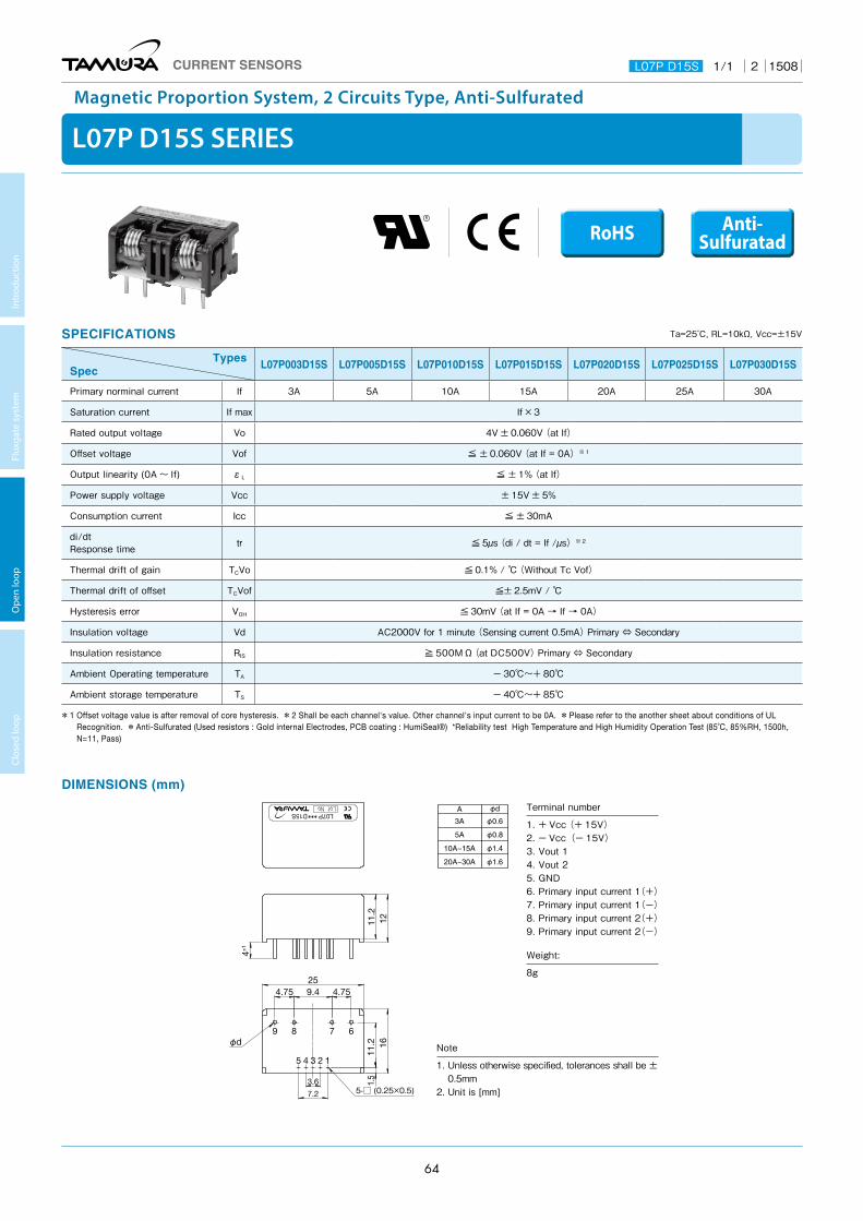
SPECIFICATIONS Ta=25˚C, RL=10kΩ, Vcc=±15V
TypesSpec L07P003D15S L07P005D15S L07P010D15S L07P015D15S L07P020D15S L07P025D15S L07P030D15S
Primary norminal current If 3A 5A 10A 15A 20A 25A 30A
Saturation current If max If×3
Rated output voltage Vo 4V ± 0.060V (at If)
Offset voltage Vof ≦ ± 0.060V (at If = 0A)※ 1
Output linearity (0A 〜 If) εL ≦ ± 1% (at If)
Power supply voltage Vcc ± 15V ± 5%
Consumption current Icc ≦ ± 30mA
di/dt Response time tr ≦ 5µs (di / dt = If /µs)※ 2
Thermal drift of gain TCVo ≦ 0.1% / ℃ (Without Tc Vof)
Thermal drift of offset TCVof ≦± 2.5mV / ℃
Hysteresis error VOH ≦ 30mV (at If = 0A → If → 0A)
Insulation voltage Vd AC2000V for 1 minute (Sensing current 0.5mA) Primary ⇔ Secondary
Insulation resistance RIS ≧ 500MΩ (at DC500V) Primary ⇔ Secondary
Ambient Operating temperature TA ー 30℃~+ 80℃
Ambient storage temperature TS ー 40℃~+ 85℃
*1 Offset voltage value is after removal of core hysteresis. *2 Shall be each channel's value. Other channel's input current to be 0A. *Please refer to the another sheet about conditions of UL Recognition. *Anti-Sulfurated (Used resistors : Gold internal Electrodes, PCB coating : HumiSeal®) *Reliability test High Temperature and High Humidity Operation Test (85˚C, 85%RH, 1500h, N=11, Pass)
L07P D15S SERIES
Magnetic Proportion System, 2 Circuits Type, Anti-Sulfurated
L07P D15S 2 15081/1
注 Note1. 指示なき寸法公差は±0.5mm
Unless otherwise specified, tolerances shall be ±0.5mm
2. 外形寸法の単位はmmとする。Unit is [mm]
A
3A
10A~15A
5A
φ0.6
φd
φ1.4
20A~30A φ1.6
φ0.8
端子番号 Terminal number
1 +Vcc (+15V)2 -Vcc(-15V) 3 Vout 14 Vout 25 GND6 Primary input current 1(+)7 Primary input current 1(-)8 Primary input current 2(+)9 Primary input current 2(-)
質量 Weight
8g
259.44.75
9
5 4 3
3.67.2 5-□ (0.25×0.5)
2 1
φd8 7 6
161211
.2
4±1
11.2
1.5
4.75
D15S L07P
DIMENSIONS (mm)
Terminal number
1. + Vcc (+ 15V)2. ー Vcc(ー 15V) 3. Vout 14. Vout 25. GND6. Primary input current 1(+)7. Primary input current 1(ー)8. Primary input current 2(+)9. Primary input current 2(ー)
Weight:
8g
Note
1. Unless otherwise specified, tolerances shall be ±0.5mm
2. Unit is [mm]
RoHS Anti-Sulfuratad
CURRENT SENSORS
Intr
oduc
tion
Flux
gate
sys
tem
O
pen
loop
Cl
osed
loop
64

259.44.75
9 8 7 6
1611
.2
4.75
5 4 3
3.67.2
2 1
φd
1.55-□ (0.25×0.5)
1211.2
4±1
A
3A
10A~15A
5A
φ0.6
φd
φ1.4
20A~30A φ1.6
φ0.8
SPECIFICATIONS Ta=25˚C, RL=10kΩ, Vcc=+5V
TypesSpec L07P003S05 L07P005S05 L07P010S05 L07P015S05 L07P020S05 L07P025S05 L07P030S05
Primary norminal current If 3A 5A 10A 15A 20A 25A 30A
Saturation current If max If×1.5
Rated output voltage Vo Vof + 1.250V ± 0.040V (at If)
Offset voltage Vof Vcc/2 ± 0.040V ※ 1 (at If = 0A)
Output linearity (0A 〜 If) εL ≦± 1% (at If)
Power supply voltage Vcc + 5V ± 5%
Consumption current Icc ≦ 30mA
di/dt Response time tr ≦ 5µs (di / dt = If /µs)※ 2
Thermal drift of gain TCVo ≦ 2mV / ℃ (Without Tc Vof)
Thermal drift of offset TCVof ≦± 2.0mV / ℃ MAX.
Hysteresis error VOH ≦ 15mV (at If = 0A → If → 0A)
Insulation voltage Vd AC2000V for 1 minute(Sensing current 0.5mA) Primary ⇔ Sacondary
Insulation resistance RIS ≧ 500MΩ (at DC500V) Primary ⇔ Sacondary
Ambient Operating temperature TA ー 30℃~+ 80℃
Ambient storage temperature TS ー 40℃~+ 85℃
*1 Offset voltage value is after removal of core hysteresis. *2 Shall be each channel's value. Other channel's input current to be 0A. *Please refer to the another sheet about conditions of UL Recognition.
DIMENSIONS (mm)
L07P S05 SERIES
Magnetic Proportion System, 2 Circuits Type
L07P S05 6 15081/1
Terminal number
1. + 5V2. NC3. OUT14. OUT25. GND6. + IN17. ー IN18. + IN29. ー IN2
Note
1. Unless otherwise specified, tolerances shall be ±0.5mm
2. Unit is [mm]
RoHS
CURRENT SENSORS
Intr
oduc
tion
Flux
gate
sys
tem
O
pen
loop
Cl
osed
loop
65

L12P D15 SERIES
Magnetic Proportion System
RoHS
7.8MAX
10.6MAX
12.8MAX
12.117.5
36.7MAX
L12P025D15 L12P050D15�
36.7MAX
12.8MAX
10.6MAX
7.8MAX
4.5
23.5MAX
0.5 φ1.4×2
4±1
4±1
14.2MIN8.8MIN
14.2MIN8.8MIN
3.9
0.31.5
8.5102.542.54
2.543
③④ ⑤ ⑥① ② ③④ ⑤ ⑥① ②
23.5MAX
4.5
0.5
1.6
3 7.622.54
10 8.52.42.4
3.91.7 0.3
Lot No.
Lot No.
SPECIFICATIONS Ta=25˚C, RL=10kΩ, Vcc=±15V
TypesSpec Symbol L12P025D15
Primary norminal current If 25A
Primary conductor specification - Φ1.4×2*1
Continuous DC current Icon 25A
Saturation current If max If×3 *2
Rated output voltage εL 4V ± 0.040V(at If)
Offset voltage Vof ≦ ± 0.040V(at If = 0A)*3
Output linearity(0A 〜 If) Vcc ≦ ± 1% (at If)
Power supply voltage Vcc ± 12V(± 5%) ~ ± 15V(± 5%)
Consumption current Icc ≦ 15mA
di/dt Response time tr ≦ 3µs (di/dt = If /µs)
Thermal drift of gain TcVo ≦ ± 0.1% / ℃ (Without Tc Vof)
Thermal drift of offset TcVof ≦± 3.0mV / ℃
Hysteresis error VOH ≦ 25mV(at If = 0A → If → 0A)
Insulation voltage Vd AC2500V for 1 minute(Sensing current 0.5mA)Primary ⇔ Secondary
Insulation resistance RIS ≧ 500MΩ (at DC500V)Primary ⇔ Secondary
Ambient Operating temperature TA ー 30℃~+ 80℃
Ambient storage temperature TS ー 40℃~+ 85℃
*1 Conductor terminals are soldered together. *2 Also operate at Vcc = ± 12V power supples, measuring range reduced to 2.5 x If. *3 Offset voltage value is after removal of core hysteresis.
DIMENSIONS (mm)
Terminal number
① + Vcc ( + 15V)② - Vcc ( ー 15V)③ Vout④ GND⑤ Primary input current ( + )⑥ Primary input current ( ー )
Weight:
20g
Note
1. Unless otherwise specified, tolerances shall be ±0.5mm
2. Unit is [mm]
CURRENT SENSORS L12P 6 15081/1
Intr
oduc
tion
Flux
gate
sys
tem
O
pen
loop
Cl
osed
loop
66

L32P S05(B)FS SERIES
Magnetic Proportion System / Through Type and Busbar Type
RoHS Anti-Sulfuratad
SPECIFICATIONS Ta=25℃, RL=10kΩ, Vcc=+5.0V
TypesSpec Symbol L32P050S05(B)FS L32P100S05(B)FS L32P150S05FS L32P200S05FS L32P300S05FS L32P400S05FS
Primary norminal current If 50A 100A 150A 200A 300A 400A
Saturation current If max ≧ ± 150A ≧ ± 300A ≧ ± 450A ≧ ± 600A ≧ ± 600A ≧ ± 600A
Type - Through hole type : L32PxxxS05FS Bus bar type : L32PxxxS05BFS Through hole type
Reference Voltage Vref + 2.495V ± 0.020V*1(at Rref ≥ 1MΩ. Ouput impedance : typ 200Ω)
Rated output voltage Vo Vof + 0.625V ± 0.015 (at If)
Offset voltage Vof Vref ± 0.025V(at If=0A)*2
Output linearity (0A 〜 If) εL ± 0.5% (at 0A,1/2If,If)
Power supply voltage Vcc + 5V ± 5%
Consumption current Icc ≦ 20mA
di/dt Response time tr ≦ 5µs (at di/dt=100A/µs)
Reference Temperature Characteristic TcVref ≦ ± 0.012%/ºC
Thermal drift of gain TCVO ≦ ± 1.5mV/℃ (Without TcVof)
Thermal drift of offset(at If=0A) TcVof ≦± 1.0mV/℃ ≦± 0.6mV/℃ ≦± 0.3mV/℃
Hysteresis error(at 0A → If → 0A) VOH ≦± 10mV ≦± 5.0mV ≦± 2.5mV
Insulation voltage Vd AC2500V for 1 minute(Sensing current 0.5mA)Primary ⇔ Secondary
Insulation resistance RIS ≧ 500MΩ (at DC500V)Primary ⇔ Secondary
Ambient Operating temperature TA ー 40 ~+ 85℃
Ambient storage temperature Ts ー 40 ~+ 85℃
* 1 It is possible to change Vof with an external reference voltage (between 1.5V - 2.8V providing its ability to sink or source approximately 5 mA.). If the external reference voltag is not used, the Vref pin should be left unconnected. *2 Offset voltage value is after removal of core hysteresis. *Please refer to the another sheet about conditions of UL Recognition. *Anti-Sulfurated (Used resistors : Gold internal Electrodes) *Ferrite core is used.
15.9
11
5.4
1.5
6.5
4.3
14.5
3-1.8
0.5
33
3
15
298
3.5
②⑤
④
4-φ0.5
③
①
2-φ1
⑥
14
Current direction
6
11
1.5
6.5
4.35.4
3-1.8
14.5
25.9
33
29
0.5 3 3.5
1.5 1.5
17
③
⑥
⑦
4-φ0.5
⑤ ①②
④
2-φ1⑧
14
10
Current direction
10
1.5
3.5
1
11
1.5
1
13.47
DIMENSIONS (mm)
11
1.5
6.5
4.35.4
3-1.8
14.5
③
⑥
⑦
4-φ0.5
⑤ ①②
④
2-φ1⑧
14
10
11
5.4
1.5
6.5
4.3
14.5
3-1.8
②⑤
④
4-φ0.5
③
①
2-φ1
⑥
14
Note
1. Unless otherwise specified, tolerances shall be ±0.5mm
2. Unit is [mm]
Terminal number
① Vcc (+5V)② GND③ Vout④ Vref (IN/OUT)⑤⑥ NC⑦ Primary input current (+)⑧ Primary input current (ー)
Weight
30gNote
1. Unless otherwise specified, tolerances shall be ±0.5mm
2. Unit is [mm]
Terminal number
① Vcc (+5V)② GND③ Vout④ Vref (IN/OUT)⑤⑥ NC
Weight
22g
CURRENT SENSORS L32P S05(B)FS 1 13071/1
Intr
oduc
tion
Flux
gate
sys
tem
O
pen
loop
Cl
osed
loop
67

L08P IPV/W/IPVW SERIES
Magnetic Proportion System / Through Type / Response time, dv/dt improvement type
RoHS
ABSOLUTE MAXIMUM RATINGS
Parameters Symbol Unit Value Comment
Supply voltage Vcc V ± 18V
ENVIRONMENTAL AND MECHANICAL CHARACTERISTICS
Parameters Symbol UnitValue
CommentMIN TYP MAX
Ambient operating temperature Ta ℃ - 40 + 80
Ambient storage temperature TS ℃ - 40 + 85
Mass m g 22
ISOLATION CHARACTERISTICS
Parameters Symbol Unit Value Comment
lnsulation voltage Vd ― AC2500V,for 1minute(Sensing current 0.5mA) Primary ⇔ Secondary
lnsulation Resistance RIS ― ≧ 500MΩ(at DC500V) Primary ⇔ Secondary
Case material ― ― UL94 V-0
SPECIFICATIONS Ta=+25℃,RL=10kΩ,Vcc=±15V
Parameters Symbol UnitValue
CommentMIN TYP MAX
Primary norminal current L08P050D15IPV
If A
50
L08P100D15IPV 100
L08P150D15IPV 150
L08P200D15W 200
L08P300D15IPVW 300
L08P400D15IPVW 400
L08P500D15IPVW 500
Saturation current*1 L08P050D15IPV
Ifmax A
150
L08P100D15IPV 300
L08P150D15IPV 450
L08P200D15W 600
L08P300D15IPVW 600
L08P400D15IPVW 600
L08P500D15IPVW 600
CURRENT SENSORS L08P IPV/W/IPVW 1 17031/3
Intr
oduc
tion
Flux
gate
sys
tem
O
pen
loop
Cl
osed
loop
68

SPECIFICATIONS Ta=+25℃,RL=10kΩ,Vcc=±15V
Parameters Symbol UnitValue
CommentMIN TYP MAX
Power supply voltage Vcc V ±12(±5%) ±15(±5%)
Consumption current Icc mA 14 20
Rated output voltage Vo V 3.960 4.000 4.040 at If
Offset voltage*2 Vof V - 0.030 0.000 + 0.030 at If = 0A
Hysteresis error VOH mV ± 20 at 0A → If → 0A
Thermal drift of gain TcVo %/℃ ± 0.05 Without TcVof
Thermal drift of offset L08P050D15IPV
TcVof mV/℃
± 2 at If = 0A
L08P100D15IPV ± 1
L08P150D15IPV ± 1
L08P200D15W ± 1
L08P300D15IPVW ± 1
L08P400D15IPVW ± 1
L08P500D15IPVW ± 1
Output Linearity(0A 〜 If) εL % - 1 + 1
Response time(@70% of If - 70% of Vo) tr µS 3 di/dt=100A/µS
Response time(@10% of If - 90% of Vo) L08P050D15IPV
tr µS
5 di/dt=100A/µS
L08P100D15IPV 5
L08P150D15IPV 5
L08P200D15W 5
L08P300D15IPVW 5
L08P400D15IPVW 5
L08P500D15IPVW 8
Response time(@10% of 250A - 90% of 2V) L08P500D15IPVW tr µS 7 di/dt=100A/µS
*1 If the product of 200A or less operate at Vcc = ± 12V power supplies, measuring range reduced to 2.5 x If.*2 Offset voltage value is after removal of core hysteresis.
STANDARDS
EN50178
CONNECTION
CURRENT SENSORS L08P IPV/W/IPVW 1 17032/3
Intr
oduc
tion
Flux
gate
sys
tem
O
pen
loop
Cl
osed
loop
69

Terminal number
Lot No.
Circuit boad hole dimension (View of solder surface)
Terminal number
Lot No.
L08PxxxD15IPV L08PxxxD15W/IPVW
Terminal number
1 + Vcc ( + 15V)2 - Vcc ( ー 15V)3 Vout4 GND
Weight:
20g
Note
1. Unless otherwise specified, tolerances shall be ±0.5mm
DIMENSIONS (mm)
CURRENT SENSORS L08P IPV/W/IPVW 1 17033/3
Intr
oduc
tion
Flux
gate
sys
tem
O
pen
loop
Cl
osed
loop
70
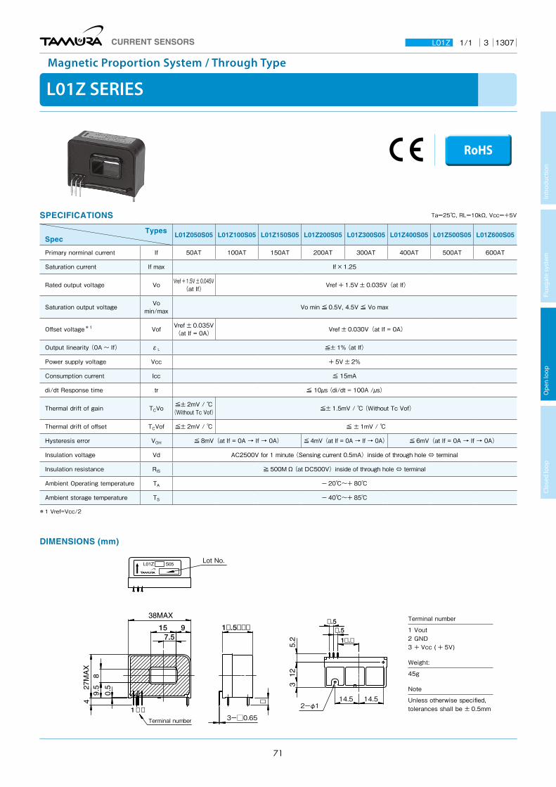
L01Z SERIES
Magnetic Proportion System / Through Type
RoHS
38MAX
15 97.5
1�.5���
�48
9.5
0.527
MA
X
5.2
3-□0.65
2-φ1
123
1 � �
�.5�.5
1�.�
14.5 14.5
L01Z S05Lot No.
Terminal number
SPECIFICATIONS Ta=25℃, RL=10kΩ, Vcc=+5V
TypesSpec
L01Z050S05 L01Z100S05 L01Z150S05 L01Z200S05 L01Z300S05 L01Z400S05 L01Z500S05 L01Z600S05
Primary norminal current If 50AT 100AT 150AT 200AT 300AT 400AT 500AT 600AT
Saturation current If max If×1.25
Rated output voltage Vo Vref + 1.5V ± 0.045V(at If) Vref + 1.5V ± 0.035V(at If)
Saturation output voltage Vomin/max Vo min ≦ 0.5V, 4.5V ≦ Vo max
Offset voltage*1 Vof Vref ± 0.035V(at If = 0A) Vref ± 0.030V(at If = 0A)
Output linearity (0A 〜 If) εL ≦± 1% (at If)
Power supply voltage Vcc + 5V ± 2%
Consumption current Icc ≦ 15mA
di/dt Response time tr ≦ 10µs (di/dt = 100A /µs)
Thermal drift of gain TCVo ≦± 2mV / ℃(Without Tc Vof) ≦± 1.5mV / ℃ (Without Tc Vof)
Thermal drift of offset TCVof ≦± 2mV / ℃ ≦ ± 1mV / ℃
Hysteresis error VOH ≦ 8mV(at If = 0A → If → 0A) ≦ 4mV(at If = 0A → If → 0A) ≦ 6mV(at If = 0A → If → 0A)
Insulation voltage Vd AC2500V for 1 minute (Sensing current 0.5mA)inside of through hole ⇔ terminal
Insulation resistance RIS ≧ 500MΩ (at DC500V)inside of through hole ⇔ terminal
Ambient Operating temperature TA ー 20℃~+ 80℃
Ambient storage temperature TS ー 40℃~+ 85℃
*1 Vref=Vcc/2
DIMENSIONS (mm)
Terminal number
1 Vout2 GND3 + Vcc ( + 5V)
Weight:
45g
Note
Unless otherwise specified, tolerances shall be ± 0.5mm
CURRENT SENSORS L01Z 3 13071/1
Intr
oduc
tion
Flux
gate
sys
tem
O
pen
loop
Cl
osed
loop
71

L37S D15 SERIES
Magnetic Proportion System / Through Type
L37S D15 2 17031/3
ABSOLUTE MAXIMUM RATINGS
Parameters Symbol Unit Value Comment
Supply voltage VCC V ± 18V
ENVIRONMENTAL AND MECHANICAL CHARACTERISTICS
Parameters Symbol UnitValue
CommentMIN TYP MAX
Ambient operating temperature Ta ℃ - 40 + 85
Ambient storage temperature TS ℃ - 40 + 85
Mass m g 62
ISOLATION CHARACTERISTICS
Parameters Symbol Unit Value Comment
Insulation voltage Vd ― AC3600V,for 1minute(Sensing current 0.5mA) Primary ⇔ Secondary
Impulse withstand voltage Vw kV 6.6
Primary ⇔ SecondaryInput waveform:・Front time 1.2µs・Time to half value 50µs・single
Insulation resistance RIS ― ≧ 1000MΩ(at DC500V) Primary ⇔ Secondary
Clearance distance dCi ― 6.5mm(MIN) Primary ⇔ Secondary
Creepage distance dCp ― 6.5mm(MIN) Primary ⇔ Secondary
Case material ― ― UL94 V-0
Comparative tracking index; (CTI) CTI V 200 ( group IIIa )
Application example
― ― 300V,CAT Ⅲ,PD2 Reinforced isolation, non uniform field according to EN50178, IEC/EN 61010-1
― ― 600V,CAT Ⅲ,PD2 Basic isolation, non uniform field according to EN50178, IEC/EN 61010-1
RoHS
CURRENT SENSORS
Intr
oduc
tion
Flux
gate
sys
tem
O
pen
loop
Cl
osed
loop
72
SPECIFICATIONS Ta=+25℃,RL=10kΩ,VCC=±15V
Parameters Symbol UnitValue
CommentMIN TYP MAX
Primary norminal current L37S050D15*
If A
Ifmax
L37S100D15* 100
L37S200D15* 200
L37S300D15* 300
L37S400D15* 400
L37S500D15* 500
L37S600D15* 600
Saturation current*1 L37S050D15*
Ifmax A
150
L37S100D15* 300
L37S200D15* 600
L37S300D15* 900
L37S400D15* 1000
L37S500D15* 1000
L37S600D15* 1000
Power supply voltage*2 Vcc V ± 12(± 5%)± 15(± 5%)
Consumption current Icc mA 15 20
Rated output voltage Vo V 3.960 4.000 4.040 at If
Offset voltage L37S050D15*
Vof V
- 0.030 0.000 + 0.030
at If = 0A
L37S100D15* - 0.020 0.000 + 0.020
L37S200D15* - 0.020 0.000 + 0.020
L37S300D15* - 0.020 0.000 + 0.020
L37S400D15* - 0.020 0.000 + 0.020
L37S500D15* - 0.020 0.000 + 0.020
L37S600D15* - 0.020 0.000 + 0.020
Hysteresis error VOH mV ± 20 at 0A → If → 0A
Thermal drift of gain TcVo %/℃ ± 0.1 Without TcVof
Thermal drift of offset L37S050D15*
TcVof mV/℃
± 2
at If = 0A
L37S100D15* ± 1
L37S200D15* ± 1
L37S300D15* ± 1
L37S400D15* ± 1
L37S500D15* ± 1
L37S600D15* ± 1
Output linearity (0A 〜 If) εL % - 1 + 1
Response time (@90% of If) tr µS 3 di/dt=100A/µs
*1 If the product of 300A or less operate at Vcc = ± 12V power supplies, measuring range reduced to 2.5 x If. *2 The power on rise time should be less than 45ms at time from 0 to + 11V.
Current sensor may not operate normally because EEPROM in sensor does not work normally.*3 Offset voltage value is after removal of core hysteresis.
L37S D15 2 17032/3CURRENT SENSORS
Intr
oduc
tion
Flux
gate
sys
tem
O
pen
loop
Cl
osed
loop
73

L37S D15 2 17033/3
STANDARDS
EN50178 , IEC/EN 61010-1 , IEC/EN 62109-1 , UL508(file № E243511)※ Please refer to the another sheet about conditions of UL Recognition.
DIMENSIONS (mm)
Order number and Connector number (terminal plating)
CONNECTION
TypesConnector
Manufacturer Part Number Old Part Number Plating of terminal
L37SxxxD15J Standard JST B4B-XH-A-G - Au
L37SxxxD15M StandardMolex
22-04-1041 5045-04A Sn
L37SxxxD15M-A Build to Order 22-11-1041 5045-04AG Au
As for the L37SxxxD15M series of a gold-plated connector, ’-A’ attaches to the end of the product name.
L37SxxxD15M L37SxxxD15J
Note
It is different from how to put the pin numbering of connector manufacturer (JST). It changes to the expression of the Molex product.
Note
Unless otherwise specified tolerances shall be ±0.5mm.
Terminal number
1 +Vcc (+15V)2 -Vcc (-15V)3 Vout4 GND
CURRENT SENSORS
Intr
oduc
tion
Flux
gate
sys
tem
O
pen
loop
Cl
osed
loop
74

L03S SERIES
Magnetic Proportion System / Through Type
RoHS
Lot No.
40.5MAX Terminal number
Connector
18.5MAX
29.5MAX
19.5MAX20.5
43
21
30.5
MA
X
15
10.5
3
39M
AX
20 20
4.5
φ2
φ4.5
φ4.5
φ2.5
L03S D15
Recommended PCB holes
DIMENSIONS (mm)
SPECIFICATIONS Ta=25˚C, RL=10kΩ, Vcc=±15V
TypesSpec L03S050D15 L03S100D15 L03S200D15 L03S300D15 L03S400D15 L03S500D15 L03S600D15
Primary norminal current If 50AT 100AT 200AT 300AT 400AT 500AT 600AT
Saturation current If max ≧± 150AT ≧± 300AT ≧± 600AT ≧± 700AT ≧± 700AT ≧± 700AT ≧± 700AT
Output voltage Vo 4V ± 0.040V(at If)
Offset voltage*1 Vof ≦± 0.040V(at If=0A) ≦± 0.030V(at If=0A)
Output linearity (without offset) εL ≦ ± 1%(at If)
Power supply voltage Vcc ± 15V ± 5%
Consumption current Icc ± 12mA (typ), ≦ ± 20mA
di/dt Response time*2 tr ≦ 10µs
Thermal drift of gain TCVo ≦± 0.1% / ℃(without Tc Vof)
Thermal drift of offset TCVof ≦± 2mV / ℃ ≦± 1mV / ℃
Hysteresis error VOH ≦ 20mV(at If = 0A → If → 0A)
Insulation voltage Vd AC2500V for 1 minute(Sensing current 0.5mA)inside of through hole ⇔ terminal
Insulation resistance RIS ≧ 500MΩ (at DC500V), inside of through hole ⇔ terminal
Ambient Operating temperature TA ー 20℃~+ 80℃
Ambient storage temperature TS ー 40℃~+ 90℃
*1 Offset voltage value is after removal of core hysteresis. *2 The smaller one on either at di/dt = 100A/us or at di/dt = If/us.
TypesConnector
Manufacturer Part Number Old Part Number Plating of terminal
L03SxxxD15 StandardMolex
22-04-1041 5045-04A Sn
L03SxxxD15-A Build to Order 22-11-1041 5045-04AG Gold
As for the product of a gold-plated connector, '-A' attaches to the end of the product name.
TAMURA recommends L37S series as a succession model.
Terminal number
1 + Vcc ( + 15V)2 - Vcc ( ー 15V)3 Vout4 GND
Weight:
50g
Note
1. Unless otherwise specified, tolerances shall be 0.5mm
CURRENT SENSORS L03S 4 15081/1
Intr
oduc
tion
Flux
gate
sys
tem
O
pen
loop
Cl
osed
loop
75

L03S D15W SERIES
Magnetic Proportion System / Through Type
RoHS
SPECIFICATIONS Ta=25˚C, RL=10kΩ, Vcc=±15V
TypesSpec
L03S050D15W L03S100D15W L03S200D15W L03S300D15W L03S400D15W L03S500D15W L03S600D15W L03S700D15W L03S800D15W
Primary norminal current If 50AT 100AT 200AT 300AT 400AT 500AT 600AT 700AT 800AT
Saturation current*1 If max ≧± 150AT ≧± 300AT ≧± 600AT ≧± 900AT ≧± 1000AT
Output voltage Vo 4V ± 0.040V(at If)
Offset voltage*2 Vof ≦± 0.040V(at If=0A) ≦± 0.030V(at If = 0A)
Output linearity(without offset) εL ≦± 1% (at If)
Power supply voltage Vcc ± 12V(± 5%)~± 15V(± 5%)
Consumption current Icc ≦± 20mA
di/dt Response time*3 tr ≦ 5us (at 90% of If ‒ 90% of Vo), ≦ 10us (at 10% of If ‒ 90% of Vo)
Thermal drift of gain TCVo ≦ 0.1% / ℃ (Without Tc Vof)
Thermal drift of offset TCVof ≦± 2mV / ℃ ≦± 1mV / ℃
Hysteresis error VOH ≦ 20mV (at If = 0A → If → 0A)
Insulation voltage Vd AC2500V for 1 minute(Sensing current 0.5mA)inside of through hole ⇔ terminal
Insulation resistance RIS ≧ 500MΩ (at DC500V), inside of through hole ⇔ terminal
Ambient Operating temperature TA ー 20℃~+ 80℃
Ambient storage temperature TS ー 40℃~+ 85℃
*1 If the product of 300A or less operate at Vcc = ± 12V power supples, measuring range reduced to 2.5 x If. *2 Offset voltage value is after removal of core hysteresis.*3 The smaller one on either at di/dt = 100A/us or at di/dt = If/us.
L03S∗∗∗D15WJ
DIMENSIONS (mm)
Types ConnectorManufacturer Part Number Old Part Number Plating of terminal
L03SxxxD15WJ Standard JST B4B-XH-A-G ‒ GoldL03SxxxD15WM Standard
Molex22-04-1041 5045-04A Sn
L03SxxxD15WM-A Build to Order 22-11-1041 5045-04AG Gold
As for L03SxxxD15WM of a gold-plated connector, '-A' attaches to the end of the product name.
Lot No.
Terminal number
connector
Recommended PCB holes
L03S∗∗∗D15WM
Lot No.
Recommended PCB holes
Terminal number
connector
TAMURA recommends L37S series as a succession model.
Terminal number
1 + Vcc ( + 15V)2 - Vcc ( ー 15V)3 Vout4 GNDNote
1. Unless otherwise specified, tolerances shall be ± 0.5mm
Weight
50g
CURRENT SENSORS L03S D15W 4 15081/1
Intr
oduc
tion
Flux
gate
sys
tem
O
pen
loop
Cl
osed
loop
76

L31S S05FS SERIES
Magnetic Proportion System / Through Type
4.75
4.5
24.5
Current direction
4 3 2 1
Terminal No.
20.5
10.5
30
40
3
Lot No.
18 11R5.5
(8.3) 19
38.8
0.2
29
2.5 6.9
9.75
Connector
φ2(BOSS)
φ4.5(HOLE)
20φ4.5
φ2.5
Recommended PCB holes
DIMENSIONS (mm)
SPECIFICATIONS Ta=25℃, RL=10kΩ, Vcc=+5.0V
TypesSpec Symbol L31S050S05FS L31S100S05FS L31S200S05FS L31S300S05FS L31S400S05FS L31S500S05FS L31S600S05FS
Primary norminal current If 50A 100A 200A 300A 400A 500A 600A
Saturation current If max ≧ ± 150A ≧ ± 300A ≧ ± 600A ≧ ± 900A ≧ ± 900A ≧ ± 900A ≧ ± 900A
Reference Voltage Vref + 2.495V ± 0.020V*1(at Rref ≥ 1MΩ. Ouput impedance : typ 200Ω)
Rated output voltage Vo Vof + 0.625V ± 0.015V(at If)
Offset voltage Vof Vref ± 0.025V(at If=0A)*2
Output linearity (0A 〜 If) εL ± 0.5% (at 0A,1/2If,If)
Power supply voltage Vcc + 5V ± 5%
Consumption current Icc ≦ 20mA
di/dt Response time tr ≦ 5µs (at di/dt=100A/µs)
Reference Temperature Characteristic TCVO ≦ ± 0.012%/ºC
Thermal drift of gain TCVof ≦ ± 1.5mV/℃ (Without TcVof)
Thermal drift of offset(at If=0A) VOH ≦ ± 1.0mV/℃ ≦ ± 0.3mV/℃
Hysteresis error(at 0A → If → 0A) Vd ≦± 10mV ≦± 2.5mV
Insulation voltage RIS AC3300V for 1 minute(Sensing current 0.5mA) Primary ⇔ Secondary
Insulation resistance TA ≧ 500MΩ (at DC500V)Primary ⇔ Secondary
Ambient Operating temperature TS ー 40 ~+ 85℃
Ambient storage temperature Ts ー 40 ~+ 85℃
* 1 It is possible to change Vof with an external reference voltage (between 1.5V - 2.8V providing its ability to sink or source approximately 5 mA.). If the external reference voltag is not used, the Vref pin should be left unconnected. *2 Offset voltage value is after removal of core hysteresis. *Please refer to the another sheet about conditions of UL Recognition. *Anti-Sulfurated(Used resistors : Gold internal Electrodes)*Ferrite core is used.
TypesConnector
Manufacturer Part Number Old Part Number Plating of terminal
L31SxxxS05FS StandardMolex
22-04-1041 5045-04A Sn
L31SxxxS05FS-A Build to Order 22-11-1041 5045-04AG Gold
As for the product of a gold-plated connector, ‘-A’ attaches to the end of the product name.
RoHS Anti-Sulfuratad
Terminal number
1 Vref (IN/OUT)2 Vout3 GND4 +Vcc (+5V)
Note
1. Unless otherwise specified, tolerances shall be ±0.5mm2. Unit is [mm]
Weight
38g
CURRENT SENSORS L31S S05FS 1 13071/1
Intr
oduc
tion
Flux
gate
sys
tem
O
pen
loop
Cl
osed
loop
77
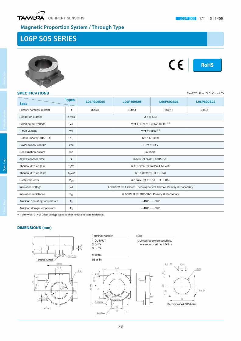
L06P S05 SERIES
Magnetic Proportion System / Through Type
RoHS
Terminal number
Lot No.
Recommended PCB holes
SPECIFICATIONS Ta=25℃, RL=10kΩ, Vcc=+5V
TypesSpec L06P300S05 L06P400S05 L06P600S05 L06P800S05
Primary norminal current If 300AT 400AT 600AT 800AT
Saturation current If max ≧ If×1.33
Rated output voltage Vo Vref + 1.5V ± 0.035V(at If)*1
Offset voltage Vof Vref ± 30mV*2
Output linearity(0A 〜 If) εL ≦± 1%(at If)
Power supply voltage Vcc + 5V ± 0.1V
Consumption current Icc ≦ 15mA
di/dt Response time tr ≦ 5µs (at di/dt = 100A /µs)
Thermal drift of gain TCVo ≦± 1.5mV/ ℃ (Without Tc Vof)
Thermal drift of offset TCVof ≦± 1.0mV/℃ (at If = 0A)
Hysteresis error VOH ≦ 10mV(at If = 0A → If → 0A)
Insulation voltage Vd AC2500V for 1 minute(Sensing current 0.5mA)Primary ⇔ Sacondary
Insulation resistance RIS ≧ 500MΩ (at DC500V)Primary ⇔ Sacondary
Ambient Operating temperature TA ー 40℃~+ 85℃
Ambient storage temperature TS ー 40℃~+ 85℃
*1 Vref=Vcc/2 *2 Offset voltage value is after removal of core hysteresis.
DIMENSIONS (mm)
Terminal number
1 OUTPUT2 GND3 + 5V
Weight:
65 ± 5g
Note
1. Unless otherwise specified, tolerances shall be ±0.5mm
CURRENT SENSORS L06P S05 3 14051/1
Intr
oduc
tion
Flux
gate
sys
tem
O
pen
loop
Cl
osed
loop
78
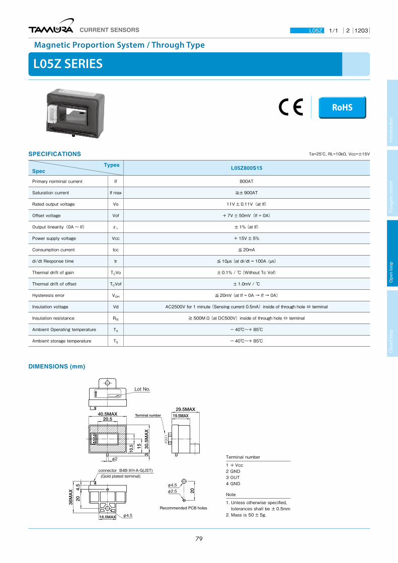
L05Z SERIES
Magnetic Proportion System / Through Type
RoHS
40.5MAX29.5MAX
19.5MAX
18.5MAX
36M
AX
30.5
MAX
20
15
20
10.5
3
4.5
20.5
φ2
φ4.5
φ4.5φ2.5
Terminal number
Lot No.
connector B4B-XH-A-G(JST)
Recommended PCB holes
(Gold plated terminal)
SPECIFICATIONS Ta=25˚C, RL=10kΩ, Vcc=±15V
TypesSpec L05Z800S15
Primary norminal current If 800AT
Saturation current If max ≧± 900AT
Rated output voltage Vo 11V ± 0.11V(at If)
Offset voltage Vof + 7V ± 50mV(If = 0A)
Output linearity(0A 〜 If) εL ± 1% (at If)
Power supply voltage Vcc + 15V ± 5%
Consumption current Icc ≦ 20mA
di/dt Response time tr ≦ 10µs (at di/dt = 100A /µs)
Thermal drift of gain TCVo ± 0.1% / ℃ (Without Tc Vof)
Thermal drift of offset TCVof ± 1.0mV / ℃
Hysteresis error VOH ≦ 20mV (at If = 0A → If → 0A)
Insulation voltage Vd AC2500V for 1 minute (Sensing current 0.5mA)inside of through hole ⇔ terminal
Insulation resistance RIS ≧ 500MΩ (at DC500V)inside of through hole ⇔ terminal
Ambient Operating temperature TA ー 40℃~+ 85℃
Ambient storage temperature TS ー 40℃~+ 85℃
DIMENSIONS (mm)
Terminal number
1 + Vcc2 GND3 OUT4 GND
Note
1. Unless otherwise specified, tolerances shall be ± 0.5mm
2. Mass is 50 ± 5g.
CURRENT SENSORS L05Z 2 12031/1
Intr
oduc
tion
Flux
gate
sys
tem
O
pen
loop
Cl
osed
loop
79

L34S D15 SERIES
Magnetic Proportion System
RoHS
17
78
33.25
11
38.75 78
19 5 1.5
Current direction
Connector
40.5
89.5
2-φ4.5(H
OLE)
64.5
40.5
1 5
65.5
5.5×4.5(SLOT HOLE)
φ4.5(H
OLE)
φ4.5(HOLE)
21
34
Terminal No.
3
53.5
10
20.5
3
(8.8)
L34S D15
Lot No.4
16
DIMENSIONS (mm)
SPECIFICATIONS Ta=25℃, RL=10kΩ, Vcc=+5.0V
TypesSpec Symbol L34S200D15 L34S300D15 L34S400D15 L34S500D15 L34S600D15 L34S800D15 L34S1T0D15 L34S1T2D15 L34S1T5D15
Primary norminal current If 200A 300A 400A 500A 600A 800A 1000A 1200A 1500A
Saturation current*1 If max ± 600A ± 900A ± 1200A ± 1500A ± 1800A ± 2400A ± 2500A ± 2500A ± 2500A
Rated Output Voltage Vo 4V ± 0.040V(at If)
Offset voltage Vof ≦± 0.020V(at If = 0A)*2
Output linearity (without offset) εL ≦± 0.5% (at 0A,1/2If,If)
Power supply voltage Vcc ± 12V (± 5%) ~ ± 15V(± 5%)
Consumption current Icc 16mA(TYP) ≦ 25mA
di/dt(@90% of If)Response time tr ≦ 5µs (di/dt = 100A /µs)*3
Thermal drift of gain TCVO ≦ ± 0.05%/℃ (Without TcVof)
Thermal drift of offset TCVof ≦ ± 1.0mV/℃ (at If=0A)
Hysteresis error VOH ≦ ± 10mV(at 0A → If → 0A)
Insulation voltage Vd AC3000V, for 1minute (Sensing current 0.5mA), inside of through hole ⇔ terminal
Insulation resistance RIS ≧ 500MΩ (at DC500V)inside of through hole ⇔ terminal
Ambient Operating temperature TA - 30℃~+ 80℃
Ambient storage temperature TS - 40℃~+ 85℃
*1 If the product of 800A or less operate at Vcc = ± 12V power supples, measuring range reduced to 2.5 x If. *2 Offset voltage value is after removal of core hysteresis. *3 Measurement condition : Primary conductor cross sectional area is as same as through hole, and penetration with 1turn in through hole. *Please refer to the another sheet about conditions of UL Recognition.
TypesConnector
Manufacturer Part Number Old Part Number Plating of terminal
L34SxxxD15 StandardMolex
22-04-1041 5045-04A Sn
L34SxxxD15-A Build to Order 22-11-1041 5045-04AG Gold
As for the product of a gold-plated connector, '-A' attaches to the end of the product name.
Terminal number
1 +Vcc (+15V)2 -Vcc (-15V)3 Vout4 GND
Note
1. Unless otherwise specified, tolerances shall be ±0.5mm
Weight
165g
CURRENT SENSORS L34 D15 3 15081/1
Intr
oduc
tion
Flux
gate
sys
tem
O
pen
loop
Cl
osed
loop
80

SPECIFICATIONS Ta=+25℃,VDD=+5V,RL≧10MΩ
Parameters Symbol UnitValue
CommentMIN TYP MAX
Measurement current range LA01M021S05
If A
- 21 21
LA01M032S05 - 31.8 31.8
LA01M035S05 - 35 35
LA01M041S05 - 41 41
Maximum primary current(RMS) Ip(RMS)max A 20
LA01M SERIES
Magnetic Proportion System / Compact size and High-speed response
LA01M 5 16011/5
ABSOLUTE MAXIMUM RATINGS
Parameters Symbol Unit Value Comment
Supply voltage VDD V 6
Jumper temperature ― ℃ 120
Output current Iout mA ± 1 Recommend ; < ± 0.5mA
ESD rating(HBM: Human Body Model) ― kV 2 C=100pF,R=1.5kΩ
ENVIRONMENTAL AND MECHANICAL CHARACTERISTICS
Parameters Symbol UnitValue
CommentMIN TYP MAX
Ambient operating temperature Ta ℃ - 40 + 90
Ambient storage temperature TS ℃ - 40 + 125
Mass m g 2
ISOLATION CHARACTERISTICS
Parameters Symbol Unit Value Comment
lnsulation voltage Vd V ≧ AC2500V,50/60Hz,for 1minute(Sensing current 0.5mA) Primary ⇔ Secondary
Impulse withstand voltage
Vw kV 2.5
Primary ⇔ SecondaryInput waveform:・Front time 1.2µs・Time to half value 50µs・single
Clearance distance dCi mm 2.0 Primary ⇔ Secondary
Creepage distance dCp mm 2.0 Primary ⇔ Secondary
Case material ― ― UL94 V-0
Comparative Tracking Index;(CTI) CTI V 200
RoHS
CURRENT SENSORS
Intr
oduc
tion
Flux
gate
sys
tem
O
pen
loop
Cl
osed
loop
81

SPECIFICATIONS Ta=+25℃,VDD=+5V,RL≧10MΩ
Parameters Symbol UnitValue
CommentMIN TYP MAX
Supply Voltage VDD V 4.5 5.0 5.5
Number of primary turns Np T 1
Primary Jumper resistance Rp mΩ 0.34
Current consumption(at Ip=0A) IDD mA 10
Offset voltage LA01M021S05
Vof V
2.390 2.500 2.610
LA01M032S05 2.408 2.500 2.592
LA01M035S05 2.423 2.500 2.577
LA01M041S05 2.432 2.500 2.568
Temperature drift of offset voltage (at Ta= - 40 〜+ 90℃,Variation from Vof(Ta=35℃),Ip=0A)
LA01M021S05
TCVo mV
± 26.0
LA01M032S05 ± 22.0
LA01M035S05 ± 17.5
LA01M041S05 ± 14.5
Sensitivity LA01M021S05
G mV/A
98.0 100.0 102.0
LA01M032S05 64.7 66.0 67.3
LA01M035S05 58.8 60.0 61.2
LA01M041S05 49.0 50.0 51.0
Temperature coefficient 1 of Sensitivity(at Ta= + 35 〜+ 90℃,Variation ratio to G(Ta=35℃))
LA01M021S05
TCG1 %
± 1.0
LA01M032S05 ± 1.0
LA01M035S05 ± 1.0
LA01M041S05 ± 2.0
Temperature coefficient 2 of Sensitivity(at Ta= - 40 ~+ 35℃,Variation ratio to G(Ta=35℃)) TCG2 % ± 2.0
Output Linearity(at 0... If) εL % - 1 1
Output noise voltage VNRMS mVrms 2.1
Ratiometric error of sensitivity VG-R % - 1 1
Ratiometric error of offset voltage Vof-R % - 1 1
Response time 1(at 90% of If ) tr µs 1 CL=100pF
Frequency bandwidth(- 3dB) BW kHz 400 CL=100pF
FUNCTIONAL BLOCK DIAGRAM
LA01M 5 16012/5CURRENT SENSORS
Intr
oduc
tion
Flux
gate
sys
tem
O
pen
loop
Cl
osed
loop
82

LA01M 5 16013/5
CHARACTERISTIC CURVE (TYP) AND PRIMARY CURRENT DERATING CURVE
CHARACTERISTICS DEFINITIONS
・Sensitivity G[mV/A],Offset voltage Vof[V]Sensitivity (G) is defined as slope of the approximate straight line by least squares method, using the data of the output voltage (Vout) when sweeping the measured current Ip at rated current range. Also Offset voltage (Vof) is defined as the intercept of the approximate straight line.
・Output linearity εL[%]Output linearity (εL) is defined as the ratio of maximum error voltage (Ve) to the full scale (F.S.) , where Vd is maximum difference between the Output voltage (Vout) and the approximate straight line calculated in the sensitivity and offset voltage definition;εL=Ve/F.S.×100
・ Ratiometric error of sensitivity VG-R[%],ratiometric error of Offset voltage Vof-R[%]Output of LA01M Series is ratiometric.Sensitivity(G) and Offset voltage(Vof) are proportional to Supply voltage (VDD).
・ Ratiometric error is defined as follows in the supply voltage range (4.5V<VDD1<5.5V);VG-R =100×[(G(VDD=VDD1)/G(VDD=5V))-(VDD1/5)]/(VDD1/5)Vof-R =100×[Vof(VDD=VDD1)-Vof(VDD=5V)×(VDD1/5)]/F.S.
Conditions: Mounted on the test board complying with the EIA/JEDEC Standards (EIA/JESD51.)
CURRENT SENSORS
Intr
oduc
tion
Flux
gate
sys
tem
O
pen
loop
Cl
osed
loop
83

TERMINAL DESCRIPTIONS
DIMENSIONS (mm)
Terminals : CuPlating for Terminals : Sn (100%)Package : RoHS compliant, halogen free
RECOMMENDED THROUGH-HOLE LAYOUTS (mm)
Note) If 2 or more trace layers are used as the current path, please make enough number of through-holes to flow current between the trace layers.
Note1)The tolerances of dimensions without any mention are ± 0.1mm.Note2)The adhesive material(RoHS compliant, halogen free)is used for holding the magnetic core.
Terminal number
① DATA_IO Test pin(connect to GND) ② VDD Power supply(5V)③ VSS GND(0V) ④ Vout Analog output⑤ SCLK Test pin(connect to GND)⑥ P Input ⑦ N Output
LA01M 5 16014/5CURRENT SENSORS
Intr
oduc
tion
Flux
gate
sys
tem
O
pen
loop
Cl
osed
loop
84
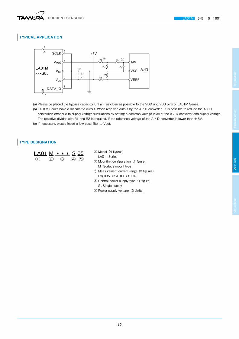
TYPICAL APPLICATION
TYPE DESIGNATION
(a) Please be placed the bypass capacitor 0.1μF as close as possible to the VDD and VSS pins of LA01M Series.(b) LA01M Series have a ratiometric output. When received output by the A / D converter , it is possible to reduce the A / D
conversion error due to supply voltage fluctuations by setting a common voltage level of the A / D converter and supply voltage. The resistive divider with R1 and R2 is required, if the reference voltage of the A / D converter is lower than + 5V.
(c) If necessary, please insert a low-pass filter to Vout.
① Model(4 figures) LA01:Series
② Mounting configuration(1 figure) M:Surface mount type
③ Measurement current range(3 figures) Ex) 035:35A 100:100A
④ Control power supply type(1 figure) S:Single supply
⑤ Power supply voltage(2 digits)
LA01M 5 16015/5CURRENT SENSORS
Intr
oduc
tion
Flux
gate
sys
tem
O
pen
loop
Cl
osed
loop
85

LA01P SERIES
Magnetic Proportion System / Compact size and High-speed response
RoHS
ABSOLUTE MAXIMUM RATINGS
Parameters Symbol Unit Value Comment
Supply voltage VDD V 6
Jumper temperature ― ℃ 120
Output current Iout mA ± 1 Recommend ; < ± 0.5mA
ESD rating(HBM: Human Body Model) ― kV 2 C=100pF,R=1.5kΩ
ENVIRONMENTAL AND MECHANICAL CHARACTERISTICS
Parameters Symbol UnitValue
CommentMIN TYP MAX
Ambient operating temperature Ta ℃ - 40 + 90
Ambient storage temperature TS ℃ - 40 + 125
Mass m g 12
ISOLATION CHARACTERISTICS
Parameters Symbol Unit Value Comment
lnsulation voltage Vd V ≧ AC2500V,50/60Hz,for 1minute(Sensing current 0.5mA) Primary ⇔ Secondary
Impulse withstand voltage
Vw kV 2.5
Primary ⇔ SecondaryInput waveform:・Front time 1.2µs・Time to half value 50µs・single
Clearance distance dCi mm 2.7 Primary ⇔ Secondary
Creepage distance dCp mm 2.7 Primary ⇔ Secondary
Case material ― ― UL94 V-0
Comparative Tracking Index;(CTI) CTI V 200
SPECIFICATIONS Ta=+25℃,VDD=+5V,RL≧10MΩ
Parameters Symbol UnitValue
CommentMIN TYP MAX
Measurement current range LA01P035S05
If A
- 35 35
LA01P046S05 - 46 46
LA01P054S05 - 54 54
LA01P085S05 - 85 85
CURRENT SENSORS LA01P 7 16121/5
Intr
oduc
tion
Flux
gate
sys
tem
O
pen
loop
Cl
osed
loop
86

SPECIFICATIONS Ta=+25℃,VDD=+5V,RL≧10MΩ
Parameters Symbol UnitValue
CommentMIN TYP MAX
Maximum primary current(RMS) Ip(RMS)max A 50 *1
Supply Voltage VDD V 4.5 5.0 5.5
Number of primary turns Np T 1
Primary Jumper resistance Rp mΩ 0.10
Current consumption(at Ip=0A) IDD mA 10
Offset voltage LA01P035S05
Vof V
2.408 2.500 2.592
LA01P046S05 2.423 2.500 2.577
LA01P054S05 2.432 2.500 2.568
LA01P085S05 2.451 2.500 2.549
Temperature drift of offset voltage (at Ta= - 40 〜+ 90℃,Variation from Vof(Ta=35℃),Ip=0A)
LA01P035S05
TCVo mV
± 21.5
LA01P046S05 ± 17.0
LA01P054S05 ± 14.0
LA01P085S05 ± 9.0
Sensitivity LA01P035S05
G mV/A
58.8 60.0 61.2
LA01P046S05 44.1 45.0 45.9
LA01P054S05 39.2 40.0 40.8
LA01P085S05 24.5 25.0 25.5
Temperature coefficient 1 of Sensitivity(at Ta= + 35 〜+ 90℃,Variation ratio to G(Ta=35℃))
LA01P035S05
TCG1 %
± 1
LA01P046S05 ± 2
LA01P054S05 ± 1
LA01P085S05 ± 1
Temperature coefficient 2 of Sensitivity(at Ta= - 40 ~+ 35℃,Variation ratio to G(Ta=35℃)) TCG2 % ± 2
Output Linearity(at 0... If) εL % - 1 1
Output noise voltage VNRMS mVrms 2.1
Ratiometric error of sensitivity VG-R % - 1 1
Ratiometric error of offset voltage Vof-R % - 1 1
Response time 1(at 90% of If ) tr µs 1 CL=100pF
Frequency bandwidth(- 3dB) BW kHz 400 CL=100pF
*1 When Ip(RMS)max is bigger than the value of If, Ip(RMS)max restricts it to the value of If.
FUNCTIONAL BLOCK DIAGRAM
CURRENT SENSORS LA01P 7 16122/5
Intr
oduc
tion
Flux
gate
sys
tem
O
pen
loop
Cl
osed
loop
87

CHARACTERISTIC CURVE (TYP) AND PRIMARY CURRENT DERATING CURVE
CHARACTERISTICS DEFINITIONS
・Sensitivity G[mV/A],Offset voltage Vof[V]Sensitivity(G)is defined as slope of the approximate straight line by least squares method, using the data of the output voltage(Vout)when sweeping the measured current Ip at rated current range.Also Offset voltage(Vof)is defined as the intercept of the approximate straight line.
・Output linearity εL[%]Output linearity(εL)is defined as the ratio of maximum error voltage(Ve)to the full scale(F.S.) , where Vd is maximum difference between the Output voltage(Vout)and the approximate straight line calculated in the sensitivity and offset voltage definition; εL=Ve/F.S.×100
・ Ratiometric error of sensitivity VG-R[%],ratiometric error of Offset voltage Vof-R[%]Output of LA01P Series is ratiometric.Sensitivity(G)and Offset voltage(Vof)are proportional to Supply voltage
(VDD).・ Ratiometric error is defined as follows in the supply voltage range (4.5V<VDD1<5.5V);VG-R =100×[(G(VDD=VDD1)/G(VDD=5V))-(VDD1/5)]/(VDD1/5)Vof-R =100×[Vof(VDD=VDD1)-Vof(VDD=5V)×(VDD1/5)]/F.S.
Conditions: Mounted on the test board complying with the EIA/JEDEC Standards (EIA/JESD51.)
・ When Ip(RMS)max is bigger than the value of If, Ip(RMS)max restricts it to the value of If.
CURRENT SENSORS LA01P 7 16123/5
Intr
oduc
tion
Flux
gate
sys
tem
O
pen
loop
Cl
osed
loop
88
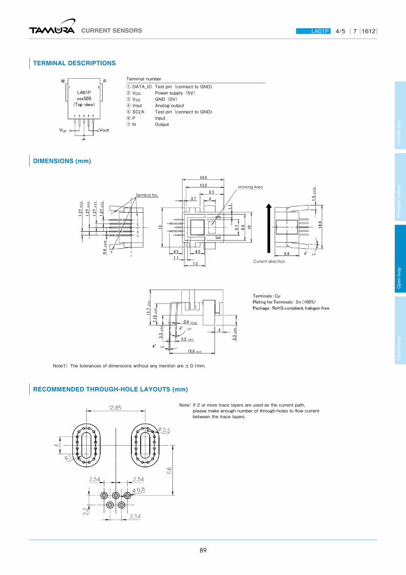
TERMINAL DESCRIPTIONS
DIMENSIONS (mm)
RECOMMENDED THROUGH-HOLE LAYOUTS (mm)
Note) If 2 or more trace layers are used as the current path, please make enough number of through-holes to flow current between the trace layers.
Note1)The tolerances of dimensions without any mention are ± 0.1mm.
Terminal number
① DATA_IO Test pin(connect to GND) ② VDD Power supply(5V)③ VSS GND(0V) ④ Vout Analog output⑤ SCLK Test pin(connect to GND)⑥ P Input ⑦ N Output
CURRENT SENSORS LA01P 7 16124/5
Intr
oduc
tion
Flux
gate
sys
tem
O
pen
loop
Cl
osed
loop
89
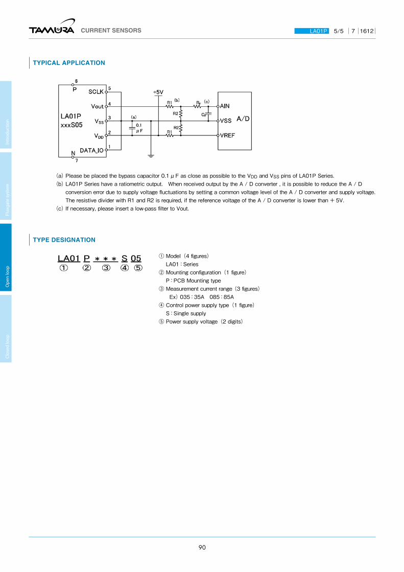
TYPICAL APPLICATION
TYPE DESIGNATION
(a) Please be placed the bypass capacitor 0.1μF as close as possible to the VDD and VSS pins of LA01P Series.(b) LA01P Series have a ratiometric output. When received output by the A / D converter , it is possible to reduce the A / D
conversion error due to supply voltage fluctuations by setting a common voltage level of the A / D converter and supply voltage. The resistive divider with R1 and R2 is required, if the reference voltage of the A / D converter is lower than + 5V.
(c) If necessary, please insert a low-pass filter to Vout.
① Model(4 figures) LA01:Series
② Mounting configuration(1 figure) P:PCB Mounting type
③ Measurement current range(3 figures) Ex) 035:35A 085:85A
④ Control power supply type(1 figure) S:Single supply
⑤ Power supply voltage(2 digits)
CURRENT SENSORS LA01P 7 16125/5
Intr
oduc
tion
Flux
gate
sys
tem
O
pen
loop
Cl
osed
loop
90
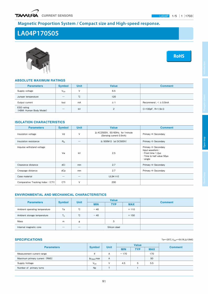
LA04P170S05
Magnetic Proportion System / Compact size and High-speed response.
ABSOLUTE MAXIMUM RATINGS
Parameters Symbol Unit Value Comment
Supply voltage VDD V 6.5
Jumper temperature ― ℃ 120
Output current Iout mA ± 1 Recommend ; < ± 0.5mA
ESD rating(HBM: Human Body Model) ― kV 2 C=100pF,R=1.5kΩ
ENVIRONMENTAL AND MECHANICAL CHARACTERISTICS
Parameters Symbol UnitValue
CommentMIN TYP MAX
Ambient operating temperature Ta ℃ - 40 + 110
Ambient storage temperature TS ℃ - 40 + 150
Mass m g 5
Internal magnetic core ― ― Silicon steel
ISOLATION CHARACTERISTICS
Parameters Symbol Unit Value Comment
lnsulation voltage Vd V ≧ AC2500V,50/60Hz,for 1minute(Sensing current 0.5mA) Primary ⇔ Secondary
Insulation resistance RIS ― ≧ 500MΩ(at DC500V) Primary ⇔ Secondary
Impulse withstand voltage
Vw kV 2.5
Primary ⇔ SecondaryInput waveform:・Front time 1.2µs・Time to half value 50µs・single
Clearance distance dCi mm 2.7 Primary ⇔ Secondary
Creepage distance dCp mm 2.7 Primary ⇔ Secondary
Case material ― ― UL94 V-0
Comparative Tracking Index;(CTI) CTI V 200
SPECIFICATIONS Ta=+25℃,VDD=+5V,RL≧10MΩ
Parameters Symbol UnitValue
CommentMIN TYP MAX
Measurement current range If A - 170 170
Maximum primary current(RMS) Ip(RMS)max A 50
Supply Voltage VDD V 4.5 5 5.5
Number of primary turns Np T 1
RoHS
CURRENT SENSORS LA04P 1 17031/5
Intr
oduc
tion
Flux
gate
sys
tem
O
pen
loop
Cl
osed
loop
91

SPECIFICATIONS Ta=+25℃,VDD=+5V,RL≧10MΩ
Parameters Symbol UnitValue
CommentMIN TYP MAX
Primary Jumper resistance Rp mΩ 0.1
Current consumption(at If) IDD mA 8.3 11
Offset voltage(at If=0A) Vof V 2.465 2.500 2.535 *1
Temperature drift of offset voltage (at Ta= -40 〜+110℃,Variation from Vof(Ta=35℃),Ip=0A) TCVof mV ± 4.0
Sensitivity G mV/A 11.8 12.0 12.2 *1
Temperature coefficient 1 of Sensitivity(at Ta= -40 〜+110℃,Variation ratio to G(Ta=35℃)) TCG % ± 0.5
Output Linearity(at 0... If) εL %F.S. - 1 1 *1
Output noise voltage VNRMS mVrms 0.5 100Hz ~ 4MHz
Ratiometric error of sensitivity VG-R % - 1 1
Ratiometric error of offset voltage Vof-R %F.S. - 0.5 0.5
Response time 1(at 90% of If ) tr µs 1.5 CL=100pF
Frequency bandwidth(-3dB) BW kHz 180 CL=100pF
*1 Please refer to Reliability Tests section to know the values after the variation and over the lifetime of this product.
FUNCTIONAL BLOCK DIAGRAM
CHARACTERISTIC CURVE (TYP) AND PRIMARY CURRENT DERATING CURVE
Conditions: Mounted on the test board complying with the EIA/JEDEC Standards (EIA/JESD51.)
CURRENT SENSORS LA04P 1 17032/5
Intr
oduc
tion
Flux
gate
sys
tem
O
pen
loop
Cl
osed
loop
92
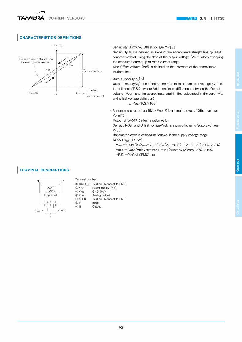
CHARACTERISTICS DEFINITIONS
・Sensitivity G[mV/A],Offset voltage Vof[V]Sensitivity (G) is defined as slope of the approximate straight line by least squares method, using the data of the output voltage (Vout) when sweeping the measured current Ip at rated current range.Also Offset voltage (Vof) is defined as the intercept of the approximate straight line.
・Output linearity εL[%]Output linearity(εL) is defined as the ratio of maximum error voltage (Ve) to the full scale(F.S.) , where Vd is maximum difference between the Output voltage (Vout) and the approximate straight line calculated in the sensitivity and offset voltage definition; εL=Ve/F.S.×100
・ Ratiometric error of sensitivity VG-R[%],ratiometric error of Offset voltage Vof-R[%]Output of LA04P Series is ratiometric.Sensitivity(G) and Offset voltage(Vof) are proportional to Supply voltage
(VDD). Ratiometric error is defined as follows in the supply voltage range
(4.5V<VDD1<5.5V);VG-R =100×[(G(VDD=VDD1)/G(VDD=5V))-(VDD1/5)]/(VDD1/5)Vof-R =100×[Vof(VDD=VDD1)-Vof(VDD=5V)×(VDD1/5)]/F.S.*F.S. =2×G×Ip(RMS)max
TERMINAL DESCRIPTIONS
Terminal number
① DATA_IO Test pin(connect to GND) ② VDD Power supply(5V)③ VSS GND(0V) ④ Vout Analog output⑤ SCLK Test pin(connect to GND)⑥ P Input ⑦ N Output
CURRENT SENSORS LA04P 1 17033/5
Intr
oduc
tion
Flux
gate
sys
tem
O
pen
loop
Cl
osed
loop
93
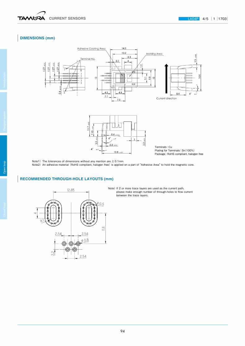
DIMENSIONS (mm)
Terminals:CuPlating for Terminals:Sn(100%)Package:RoHS compliant, halogen free
RECOMMENDED THROUGH-HOLE LAYOUTS (mm)
Note) If 2 or more trace layers are used as the current path, please make enough number of through-holes to flow current between the trace layers.
Note1)The tolerances of dimensions without any mention are ± 0.1mm.Note2)An adhesive material (RoHS compliant, halogen free) is applied on a part of “Adhesive Area” to hold the magnetic core.
CURRENT SENSORS LA04P 1 17034/5
Intr
oduc
tion
Flux
gate
sys
tem
O
pen
loop
Cl
osed
loop
94

TYPICAL APPLICATION
TYPE DESIGNATION
RELIABILITY TEST
(a) Please be placed the bypass capacitor 0.1μF as close as possible to the VDD and VSS pins of LA04P Series.(b) LA04P Series have a ratiometric output. When received output by the A/D converter , it is possible to reduce the A/D conversion error due to supply voltage fluctuations by setting a common voltage level of the A/D converter and supply voltage. The resistive divider with R1 and R2 is required, if the reference voltage of the A/D converter is lower than +5V.
(c) If necessary, please insert a low-pass filter to Vout.
① Model(4 figures) LA04:Series② Mounting configuration(1 figure)
P:PCB Mounting type③ Measurement current range(3 figures)
Ex) 170:170A④ Control power supply type(1 figure)
S:Single supply⑤ Power supply voltage(2 digits)
Tested samples are pretreated as below before each reliability test:Desiccation : 125℃/24h → Moisture Absorption: 85℃/85%RH/168h → Flow: 1time (260℃ , 10s)
Criterion for determiningProducts whose drifts before and after the reliability tests do not exceed the values below are considered to be in spec. Sensitivity G (Ta=25℃) :Within ± 1.5% Offset Voltage Vof (Ta=25℃) :Within ± 100mV Output Linearity εL (Ta=25℃) :Within ± 1% FS
CURRENT SENSORS LA04P 1 17035/5
Intr
oduc
tion
Flux
gate
sys
tem
O
pen
loop
Cl
osed
loop
95

LA02P Series
Magnetic Proportion System / Compact size and High-speed response. Vcc = +3.3V
RoHS
ABSOLUTE MAXIMUM RATINGS
Parameters Symbol Unit Value Comment
Supply voltage VDD V 6.5
Jumper temperature ― ℃ 120
Output current Iout mA ± 1 Recommend ; < ± 0.5mA
ESD rating(HBM: Human Body Model) ― kV 2 C=100pF,R=1.5kΩ
ENVIRONMENTAL AND MECHANICAL CHARACTERISTICS
Parameters Symbol UnitValue
CommentMIN TYP MAX
Ambient operating temperature Ta ℃ - 40 + 110
Ambient storage temperature TS ℃ - 40 + 150
Mass m g 5.5
Internal magnetic core ― ― Ferrite
ISOLATION CHARACTERISTICS
Parameters Symbol Unit Value Comment
lnsulation voltage Vd V ≧ AC3000V,50/60Hz,for 1minute(Sensing current 0.5mA) Primary ⇔ Secondary
Impulse withstand voltage
Vw kV 6
Primary ⇔ SecondaryInput waveform:・Front time 1.2µs・Time to half value 50µs・single
Clearance distance dCi mm 13.3 Primary ⇔ Secondary
Creepage distance dCp mm 13.3 Primary ⇔ Secondary
Case material ― ― UL94 V-0
Comparative Tracking Index;(CTI) CTI V 150
SPECIFICATIONS Ta=+25℃,VDD=+3.3V,RL≧10MΩ
Parameters Symbol UnitValue
CommentMIN TYP MAX
Measurement current range LA02P021S03
If A
- 21 21
LA02P035S03 - 35 35
LA02P054S03 - 54 54
LA02P085S03 - 85 85
CURRENT SENSORS LA02P 6 16011/5
Intr
oduc
tion
Flux
gate
sys
tem
O
pen
loop
Cl
osed
loop
96
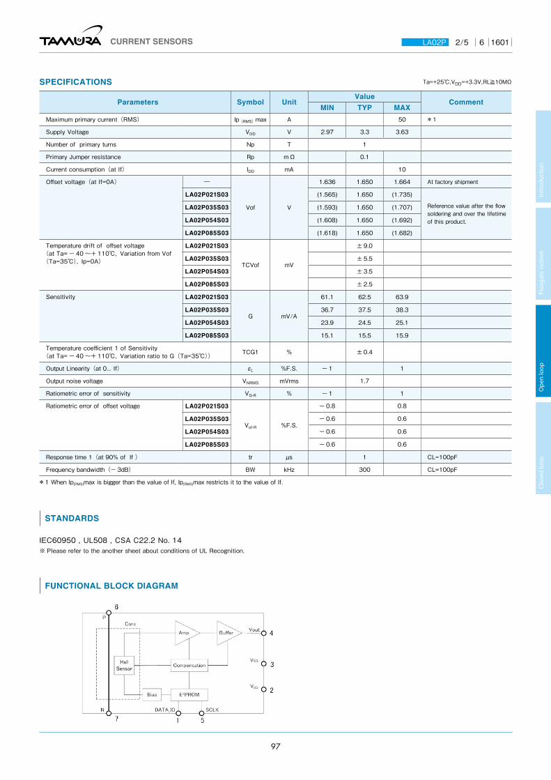
SPECIFICATIONS Ta=+25℃,VDD=+3.3V,RL≧10MΩ
Parameters Symbol UnitValue
CommentMIN TYP MAX
Maximum primary current(RMS) Ip(RMS)max A 50 *1
Supply Voltage VDD V 2.97 3.3 3.63
Number of primary turns Np T 1
Primary Jumper resistance Rp mΩ 0.1
Current consumption(at If) IDD mA 10
Offset voltage(at If=0A) ―
Vof V
1.636 1.650 1.664 At factory shipment
LA02P021S03 (1.565) 1.650 (1.735)
Reference value after the flow soldering and over the lifetime of this product.
LA02P035S03 (1.593) 1.650 (1.707)
LA02P054S03 (1.608) 1.650 (1.692)
LA02P085S03 (1.618) 1.650 (1.682)
Temperature drift of offset voltage (at Ta= - 40 〜+ 110℃,Variation from Vof(Ta=35℃),Ip=0A)
LA02P021S03
TCVof mV
± 9.0
LA02P035S03 ± 5.5
LA02P054S03 ± 3.5
LA02P085S03 ± 2.5
Sensitivity LA02P021S03
G mV/A
61.1 62.5 63.9
LA02P035S03 36.7 37.5 38.3
LA02P054S03 23.9 24.5 25.1
LA02P085S03 15.1 15.5 15.9
Temperature coefficient 1 of Sensitivity(at Ta= - 40 〜+ 110℃,Variation ratio to G(Ta=35℃)) TCG1 % ± 0.4
Output Linearity(at 0... If) εL %F.S. - 1 1
Output noise voltage VNRMS mVrms 1.7
Ratiometric error of sensitivity VG-R % - 1 1
Ratiometric error of offset voltage LA02P021S03
Vof-R %F.S.
- 0.8 0.8
LA02P035S03 - 0.6 0.6
LA02P054S03 - 0.6 0.6
LA02P085S03 - 0.6 0.6
Response time 1(at 90% of If ) tr µs 1 CL=100pF
Frequency bandwidth(- 3dB) BW kHz 300 CL=100pF
*1 When Ip(RMS)max is bigger than the value of If, Ip(RMS)max restricts it to the value of If.
FUNCTIONAL BLOCK DIAGRAM
STANDARDS
IEC60950 , UL508 , CSA C22.2 No. 14※ Please refer to the another sheet about conditions of UL Recognition.
CURRENT SENSORS LA02P 6 16012/5
Intr
oduc
tion
Flux
gate
sys
tem
O
pen
loop
Cl
osed
loop
97
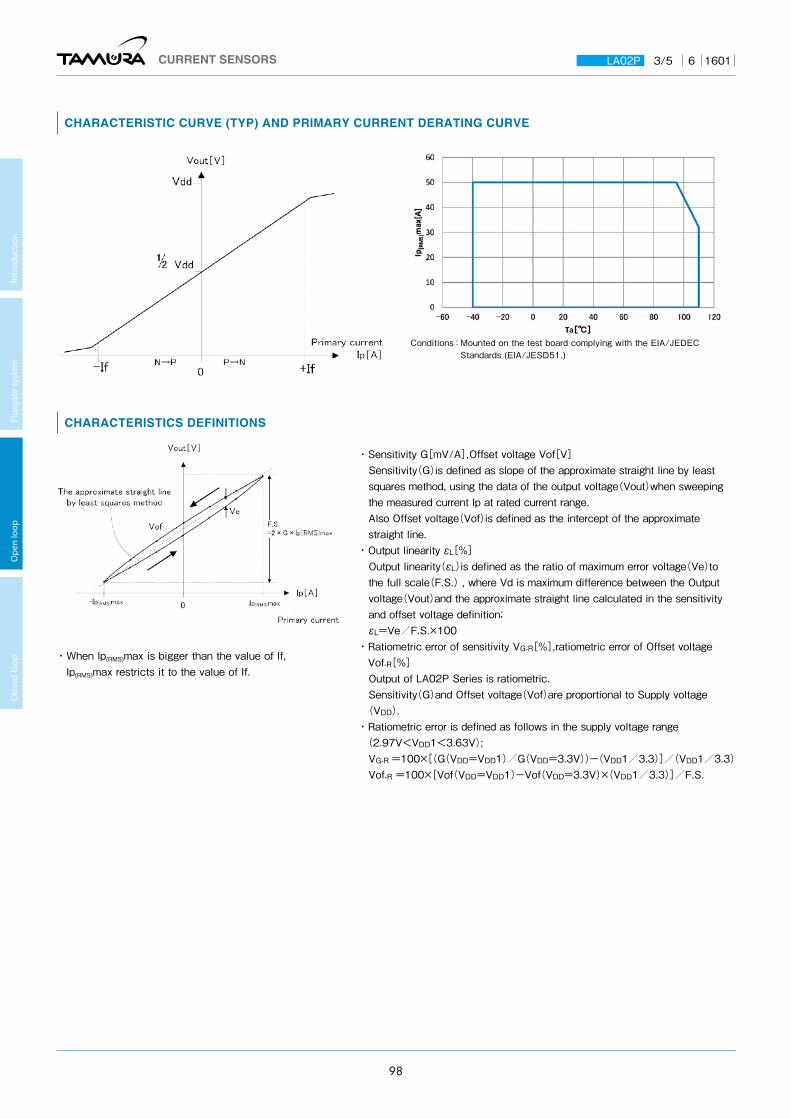
CHARACTERISTIC CURVE (TYP) AND PRIMARY CURRENT DERATING CURVE
CHARACTERISTICS DEFINITIONS
・Sensitivity G[mV/A],Offset voltage Vof[V]Sensitivity(G)is defined as slope of the approximate straight line by least squares method, using the data of the output voltage(Vout)when sweeping the measured current Ip at rated current range.Also Offset voltage(Vof)is defined as the intercept of the approximate straight line.
・Output linearity εL[%]Output linearity(εL)is defined as the ratio of maximum error voltage(Ve)to the full scale(F.S.) , where Vd is maximum difference between the Output voltage(Vout)and the approximate straight line calculated in the sensitivity and offset voltage definition; εL=Ve/F.S.×100
・ Ratiometric error of sensitivity VG-R[%],ratiometric error of Offset voltage Vof-R[%]Output of LA02P Series is ratiometric.Sensitivity(G)and Offset voltage(Vof)are proportional to Supply voltage
(VDD).・ Ratiometric error is defined as follows in the supply voltage range (2.97V<VDD1<3.63V);VG-R =100×[(G(VDD=VDD1)/G(VDD=3.3V))-(VDD1/3.3)]/(VDD1/3.3)Vof-R =100×[Vof(VDD=VDD1)-Vof(VDD=3.3V)×(VDD1/3.3)]/F.S.
Conditions: Mounted on the test board complying with the EIA/JEDEC Standards (EIA/JESD51.)
・ When Ip(RMS)max is bigger than the value of If, Ip(RMS)max restricts it to the value of If.
CURRENT SENSORS LA02P 6 16013/5
Intr
oduc
tion
Flux
gate
sys
tem
O
pen
loop
Cl
osed
loop
98

TERMINAL DESCRIPTIONS
DIMENSIONS (mm)
Terminals:CuPlating for Terminals:Sn(100%)Package:RoHS compliant, halogen free
RECOMMENDED THROUGH-HOLE LAYOUTS (mm)
Note) If 2 or more trace layers are used as the current path, please make enough number of through-holes to flow current between the trace layers.
Note1)The tolerances of dimensions without any mention are ± 0.1mm.
Terminal number
① DATA_IO Test pin(connect to GND) ② VDD Power supply(3.3V)③ VSS GND(0V) ④ Vout Analog output⑤ SCLK Test pin(connect to GND)⑥ P Input ⑦ N Output
CURRENT SENSORS LA02P 6 16014/5
Intr
oduc
tion
Flux
gate
sys
tem
O
pen
loop
Cl
osed
loop
99

TYPICAL APPLICATION
TYPE DESIGNATION
(a) Please be placed the bypass capacitor 0.1μF as close as possible to the VDD and VSS pins of LA02P Series.(b) LA02P Series have a ratiometric output. When received output by the A / D converter , it is possible to reduce the A / D conversion error due to supply voltage fluctuations by setting a common voltage level of the A / D converter and supply voltage. The resistive divider with R1 and R2 is required, if the reference voltage of the A / D converter is lower than + 3.3V.
(c) If necessary, please insert a low-pass filter to Vout.
① Model(4 figures) LA02:Series② Mounting configuration(1 figure)
P:PCB Mounting type③ Measurement current range(3 figures)
Ex) 035:35A 085:85A④ Control power supply type(1 figure)
S:Single supply⑤ Power supply voltage(2 digits)
RELIABILITY TEST
Tested samples are pretreated as below before each reliability test:Desiccation : 125℃ /24h → Moisture Absorption : 85℃ /85%RH/168h → Flow : 1 time (260℃ , 10s)
Criterion for determiningProducts whose drifts before and after the reliability tests do not exceed the values below are considered to be in spec. Sensitivity G (Ta=25℃ ) :Within ± 1.5% (All model) Offset Voltage Vof (Ta=25℃ ) :Within ± 100mV (LA02P021S03), Within ± 66mV (Other model) Output Linearity εL (Ta=25℃ ) :Within ± 1% (All model)
CURRENT SENSORS LA02P 6 16015/5
Intr
oduc
tion
Flux
gate
sys
tem
O
pen
loop
Cl
osed
loop
100

LA03P Series
Magnetic Proportion System / Compact size and High-speed response. Vcc = +5.0V
ABSOLUTE MAXIMUM RATINGS
Parameters Symbol Unit Value Comment
Supply voltage VDD V 6.5
Jumper temperature ― ℃ 120
Output current Iout mA ± 1 Recommend ; < ± 0.5mA
ESD rating(HBM: Human Body Model) ― kV 2 C=100pF,R=1.5kΩ
ENVIRONMENTAL AND MECHANICAL CHARACTERISTICS
Parameters Symbol UnitValue
CommentMIN TYP MAX
Ambient operating temperature Ta ℃ - 40 + 110
Ambient storage temperature TS ℃ - 40 + 150
Mass m g 5.5
Internal magnetic core ― ― Ferrite
ISOLATION CHARACTERISTICS
Parameters Symbol Unit Value Comment
lnsulation voltage Vd V ≧ AC3000V,50/60Hz,for 1minute(Sensing current 0.5mA) Primary ⇔ Secondary
Impulse withstand voltage
Vw kV 6
Primary ⇔ SecondaryInput waveform:・Front time 1.2µs・Time to half value 50µs・single
Clearance distance dCi mm 13.3 Primary ⇔ Secondary
Creepage distance dCp mm 13.3 Primary ⇔ Secondary
Case material ― ― UL94 V-0
Comparative Tracking Index;(CTI) CTI V 150
SPECIFICATIONS Ta=+25℃,VDD=+5V,RL≧10MΩ
Parameters Symbol UnitValue
CommentMIN TYP MAX
Measurement current range LA03P021S05
If A
- 21 21
LA03P035S05 - 35 35
LA03P054S05 - 54 54
LA03P085S05 - 85 85
RoHS
CURRENT SENSORS LA03P 6 16011/5
Intr
oduc
tion
Flux
gate
sys
tem
O
pen
loop
Cl
osed
loop
101

SPECIFICATIONS Ta=+25℃,VDD=+5V,RL≧10MΩ
Parameters Symbol UnitValue
CommentMIN TYP MAX
Maximum primary current(RMS) Ip(RMS)max A 50 *1
Supply Voltage VDD V 4.5 5.0 5.5
Number of primary turns Np T 1
Primary Jumper resistance Rp mΩ 0.1
Current consumption(at If) IDD mA 11
Offset voltage(at If=0A) ―
Vof V
2.480 2.500 2.520 At factory shipment
LA03P021S05 (2.350) 2.500 (2.650)
Reference value after the flow soldering and over the lifetime of this product.
LA03P035S05 (2.400) 2.500 (2.600)
LA03P054S05 (2.425) 2.500 (2.575)
LA03P085S05 (2.445) 2.500 (2.555)
Temperature drift of offset voltage (at Ta= - 40 〜+ 110℃,Variation from Vof(Ta=35℃),Ip=0A)
LA03P021S05
TCVof mV
± 23.0
LA03P035S05 ± 12.0
LA03P054S05 ± 8.0
LA03P085S05 ± 6.0
Sensitivity LA03P021S05
G mV/A
98.0 100.0 102.0
LA03P035S05 58.8 60.0 61.2
LA03P054S05 39.2 40.0 40.8
LA03P085S05 24.4 25.0 25.6
Temperature coefficient 1 of Sensitivity(at Ta= - 40 〜+ 110℃,Variation ratio to G(Ta=35℃)) TCG1 % ± 0.5
Output Linearity(at 0... If) εL %F.S. - 1 1
Output noise voltage VNRMS mVrms 1.7
Ratiometric error of sensitivity VG-R % - 1 1
Ratiometric error of offset voltage LA03P021S05
Vof-R %F.S.
- 0.7 0.7
LA03P035S05 - 0.5 0.5
LA03P054S05 - 0.5 0.5
LA03P085S05 - 0.5 0.5
Response time 1(at 90% of If ) tr µs 1 CL=100pF
Frequency bandwidth(- 3dB) BW kHz 300 CL=100pF
*1 When Ip(RMS)max is bigger than the value of If, Ip(RMS)max restricts it to the value of If.
FUNCTIONAL BLOCK DIAGRAM
STANDARDS
IEC60950 , UL508 , CSA C22.2 No. 14※ Please refer to the another sheet about conditions of UL Recognition.
CURRENT SENSORS LA03P 6 16012/5
Intr
oduc
tion
Flux
gate
sys
tem
O
pen
loop
Cl
osed
loop
102
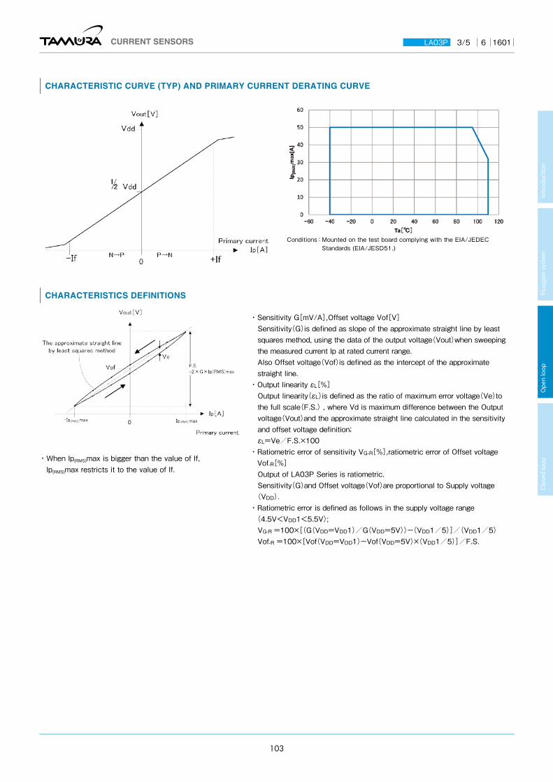
CHARACTERISTIC CURVE (TYP) AND PRIMARY CURRENT DERATING CURVE
CHARACTERISTICS DEFINITIONS
・Sensitivity G[mV/A],Offset voltage Vof[V]Sensitivity(G)is defined as slope of the approximate straight line by least squares method, using the data of the output voltage(Vout)when sweeping the measured current Ip at rated current range.Also Offset voltage(Vof)is defined as the intercept of the approximate straight line.
・Output linearity εL[%]Output linearity(εL)is defined as the ratio of maximum error voltage(Ve)to the full scale(F.S.) , where Vd is maximum difference between the Output voltage(Vout)and the approximate straight line calculated in the sensitivity and offset voltage definition; εL=Ve/F.S.×100
・ Ratiometric error of sensitivity VG-R[%],ratiometric error of Offset voltage Vof-R[%]Output of LA03P Series is ratiometric.Sensitivity(G)and Offset voltage(Vof)are proportional to Supply voltage
(VDD).・ Ratiometric error is defined as follows in the supply voltage range (4.5V<VDD1<5.5V);VG-R =100×[(G(VDD=VDD1)/G(VDD=5V))-(VDD1/5)]/(VDD1/5)Vof-R =100×[Vof(VDD=VDD1)-Vof(VDD=5V)×(VDD1/5)]/F.S.
Conditions: Mounted on the test board complying with the EIA/JEDEC Standards (EIA/JESD51.)
・ When Ip(RMS)max is bigger than the value of If, Ip(RMS)max restricts it to the value of If.
CURRENT SENSORS LA03P 6 16013/5
Intr
oduc
tion
Flux
gate
sys
tem
O
pen
loop
Cl
osed
loop
103
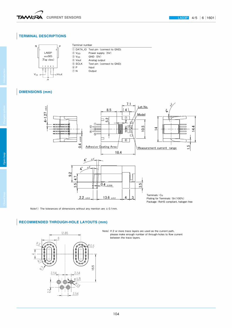
TERMINAL DESCRIPTIONS
DIMENSIONS (mm)
Terminals:CuPlating for Terminals:Sn(100%)Package:RoHS compliant, halogen free
RECOMMENDED THROUGH-HOLE LAYOUTS (mm)
Note) If 2 or more trace layers are used as the current path, please make enough number of through-holes to flow current between the trace layers.
Note1)The tolerances of dimensions without any mention are ± 0.1mm.
Terminal number
① DATA_IO Test pin(connect to GND) ② VDD Power supply(5V)③ VSS GND(0V) ④ Vout Analog output⑤ SCLK Test pin(connect to GND)⑥ P Input ⑦ N Output
CURRENT SENSORS LA03P 6 16014/5
Intr
oduc
tion
Flux
gate
sys
tem
O
pen
loop
Cl
osed
loop
104

TYPICAL APPLICATION
TYPE DESIGNATION
RELIABILITY TEST
(a) Please be placed the bypass capacitor 0.1μF as close as possible to the VDD and VSS pins of LA03P Series.(b) LA03P Series have a ratiometric output. When received output by the A / D converter , it is possible to reduce the A / D conversion error due to supply voltage fluctuations by setting a common voltage level of the A / D converter and supply voltage. The resistive divider with R1 and R2 is required, if the reference voltage of the A / D converter is lower than + 5V.
(c) If necessary, please insert a low-pass filter to Vout.
① Model(4 figures) LA03:Series② Mounting configuration(1 figure)
P:PCB Mounting type③ Measurement current range(3 figures)
Ex) 035:35A 085:85A④ Control power supply type(1 figure)
S:Single supply⑤ Power supply voltage(2 digits)
Tested samples are pretreated as below before each reliability test:Desiccation : 125℃ /24h → Moisture Absorption : 85℃ /85%RH/168h → Flow : 1 time (260℃ , 10s)
Criterion for determiningProducts whose drifts before and after the reliability tests do not exceed the values below are considered to be in spec. Sensitivity G (Ta=25℃ ) :Within ± 1.5% (All model) Offset Voltage Vof (Ta=25℃ ) :Within ± 150mV (LA03P021S05), Within ± 100mV (Other model) Output Linearity εL (Ta=25℃ ) :Within ± 1% (All model)
CURRENT SENSORS LA03P 6 16015/5
Intr
oduc
tion
Flux
gate
sys
tem
O
pen
loop
Cl
osed
loop
105

S22P M2 SERIES
Servo system / Voltage-output type External magnetic field improvement type
4OUT
1 2 3
6 5
IN
4OUT
1 2 3
6 5
IN
6 5
1 2 3
OUT
IN
4
23.5
0.5
22.2
5.5
3-(0.5×0.25)10
0.8
5.08
12.7
123 4
56
IN OUT
+5V
G Vout
3.5
0.7
24
2.54 2.54
7.66 5.08 7.6 1.9
Lot N
o.
***
If/2
If
If/3
SPECIFICATIONS Ta=25℃, RL=10kΩ, Vcc=+5V
TypesSpec S22P006S05M2 S22P015S05M2 S22P025S05M2
Primary norminal current If 6A 15A 25A
Saturation current If max ± 18A ± 45A ± 75A
Rated output voltage Vo Vof ± 0.625V(at If)
Output voltage accuracy XG 0.625V ± 0.010V(at If)
Offset voltage*1 Vof 2.5V ± 0.050V(at If = 0A) 2.5V ± 0.020V(at If = 0A) 2.5V ± 0.015V(at If = 0A)
Output linearity εL ≦± 0.2%(at If)
Power supply voltage Vcc + 5V ± 5%
Consumption current Icc Typ. 12.5mA (If=0A) + 37.5mA(If max)
di/dt Response time(@90% of If) tr ≦ 1µs (at di / dt = If /µs)
Thermal drift of gain TCVo ≦ ± 0.05mV / ℃ (Without TcVof)
Thermal drift of offset TcVof ー 10 ~ 25℃:± 1.6mV / ℃ 25 ~ 85℃:± 0.8mV / ℃
ー 10 ~ 25℃:± 0.6mV / ℃ 25 ~ 85℃:± 0.3mV / ℃
ー 10 ~ 25℃:± 0.4mV / ℃ 25 ~ 85℃:± 0.2mV / ℃
Hysteresis error VOH ≦ 0.5mV (at If = 0A → If → 0A)
Insulation voltage Vd AC3000V for 1 minute (Sensing current 0.5mA)Primary ⇔ Sacondary
Insulation resistance RIS ≧ 500MΩ (at DC500V)Primary ⇔ Sacondary
Ambient Operating temperature TA ー 10℃~+ 85℃
Ambient storage temperature TS ー 25℃~+ 100℃
*1 Offset voltage value is after removal of core hysteresis. * Please refer to the another sheet about conditions of UL Recognition.
DIMENSIONS (mm)
RoHS
Note
1. Unless otherwise specified, tolerances shall be ±0.5mm
2. Unit is [mm]
Weight:
8g typ
CURRENT SENSORS S22P M2 4 12091/1
Intr
oduc
tion
Flux
gate
sys
tem
O
pen
loop
Cl
osed
loop
106

S22P P SERIES
Servo system / Voltage-output type / Short lead model
Tolerance : ±0.5Unit : mm
23.5
0.5
22.2
3-(□0.5×0.25)
OUT
IN
1.85 7.62 2.542.54×2=5.08
3-0.7
3.5
0.8
3.5 17.2
11 ⑥ ⑤ ④
① ② ③
⑦
⑨⑧
3.5
5.08
12.7
2.54
10
2 3
6 5 4OUT
1IN
2 3
6 5 4OUT
1IN
2 3
OUT
IN
6 5
1
4
If/2
If
If/3
SPECIFICATIONS Ta=25℃, RL=10kΩ, Vcc=+5V
TypesSpec S22P006S05P S22P015S05P S22P025S05P
Primary norminal current If 6A 15A 25A
Saturation current If max ± 18A ± 45A ± 75A
Rated output voltage Vo Vof ± 0.625V(at If)
Output voltage accuracy XG 0.625V ± 0.010V(at If)
Offset voltage*1 Vof 2.5V ± 0.050V(at If = 0 A) 2.5V ± 0.020V(at If = 0 A) 2.5V ± 0.015V(at If = 0 A)
Output linearity εL ≦± 0.2%(at If)
Power supply voltage Vcc + 5V ± 5%
Consumption current Icc Typ.12.5mA(If=0A)+ 37.5mA(If max)
di / dt Response time (@90% of If) tr ≦ 1µs(di/dt = If /µs)
Thermal drift of gain TCVo ≦ ± 0.05mV / ℃ (Without TcVof)
Thermal drift of offset TcVof ー 10 ~ 25℃:± 1.6mV / ℃ 25 ~ 85℃:± 0.8mV / ℃
ー 10 ~ 25℃:± 0.6mV / ℃ 25 ~ 85℃:± 0.3mV / ℃
ー 10 ~ 25℃:± 0.4mV / ℃ 25 ~ 85℃:± 0.2mV / ℃
Hysteresis error VOH ≦ 0.5mV(at If = 0A → If → 0A)
Insulation voltage Vd AC3000V for 1 minute (Sensing current 0.5mA)Primary ⇔ Sacondary
Insulation resistance RIS ≧ 500MΩ (at DC500V)Primary ⇔ Sacondary
Ambient Operating temperature TA ー 10℃~+ 85℃
Ambient storage temperature TS ー 25℃~+ 100℃
*1 Offset voltage value is after removal of core hysteresis. * Please refer to the another sheet about conditions of UL Recognition.
DIMENSIONS (mm)
RoHS
Terminal number
① IN-1② IN-2③ IN-3④ OUT-3⑤ OUT-2⑥ OUT-1⑦ Vout⑧ GND⑨ + Vcc ( + 5V)
Weight:
8g typ
Note
1. Unless otherwise specified, tolerances shall be ±0.5mm
2. Unit is [mm]
CURRENT SENSORS S22P P 1 14051/1
Intr
oduc
tion
Flux
gate
sys
tem
O
pen
loop
Cl
osed
loop
107
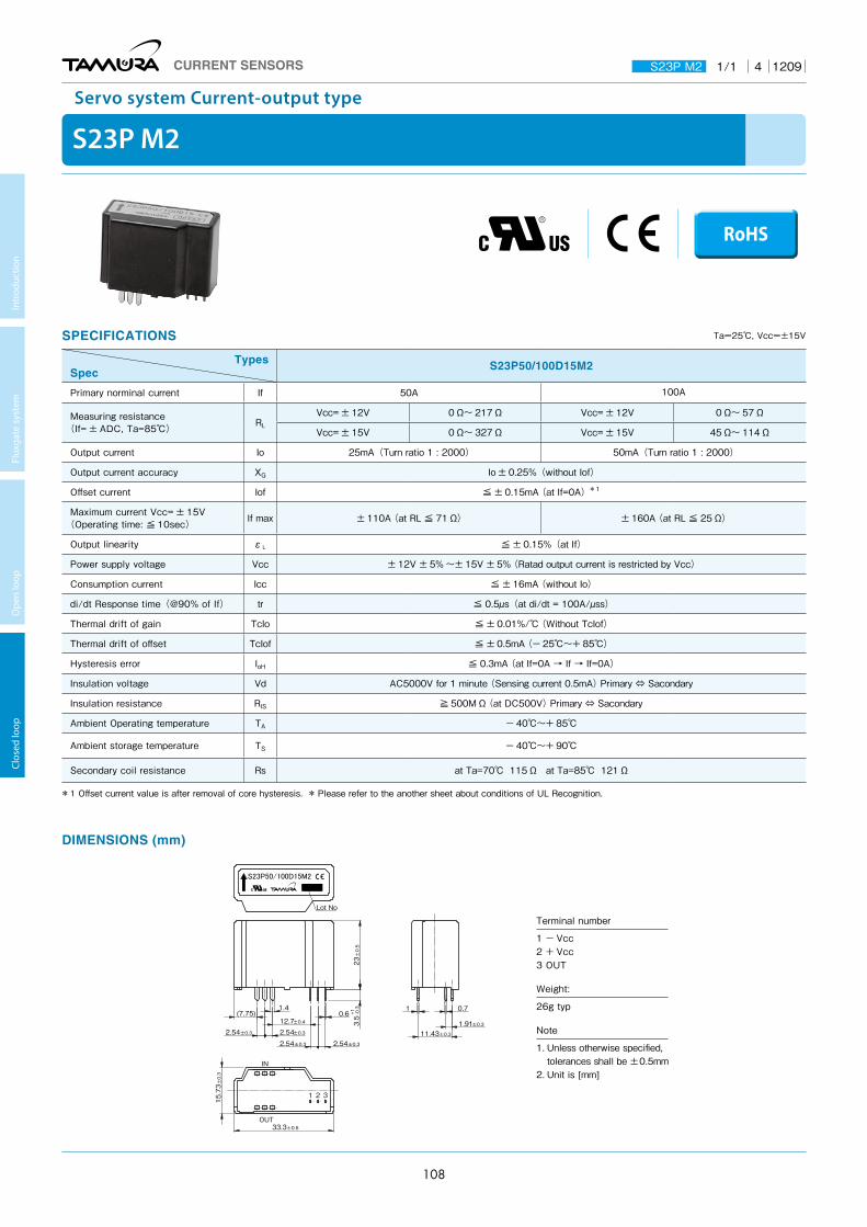
S23P M2
Servo system Current-output type
12.72.54±0.3
0.6
2.54±0.3
1.4
2.54±0.32.54±0.3
(7.75)±0.4 3.
5-0.3+1
23±0.5
1 0.7
1.91±0.311.43±0.3
IN
OUT
1 2 3
33.3±0.5
15.73±0.3
Lot No
SPECIFICATIONS Ta=25℃, Vcc=±15V
TypesSpec
S23P50/100D15M2
Primary norminal current If 50A 100A
Measuring resistance(If= ± ADC, Ta=85℃) RL
Vcc= ± 12V 0Ω~ 217Ω Vcc= ± 12V 0Ω~ 57Ω
Vcc= ± 15V 0Ω~ 327Ω Vcc= ± 15V 45Ω~ 114Ω
Output current Io 25mA(Turn ratio 1 : 2000) 50mA(Turn ratio 1 : 2000)
Output current accuracy XG Io ± 0.25%(without Iof)
Offset current Iof ≦ ± 0.15mA (at If=0A)*1
Maximum current Vcc= ± 15V(Operating time: ≦ 10sec) If max ± 110A (at RL ≦ 71Ω) ± 160A (at RL ≦ 25Ω)
Output linearity εL ≦ ± 0.15%(at If)
Power supply voltage Vcc ± 12V ± 5% ~± 15V ± 5% (Ratad output current is restricted by Vcc)
Consumption current Icc ≦ ± 16mA (without Io)
di/dt Response time(@90% of If) tr ≦ 0.5µs(at di/dt = 100A/µss)
Thermal drift of gain TcIo ≦ ± 0.01%/℃ (Without TcIof)
Thermal drift of offset TcIof ≦ ± 0.5mA (ー 25℃~+ 85℃)
Hysteresis error IoH ≦ 0.3mA (at If=0A → If → If=0A)
Insulation voltage Vd AC5000V for 1 minute (Sensing current 0.5mA) Primary ⇔ Sacondary
Insulation resistance RIS ≧ 500MΩ (at DC500V) Primary ⇔ Sacondary
Ambient Operating temperature TA ー 40℃~+ 85℃
Ambient storage temperature TS ー 40℃~+ 90℃
Secondary coil resistance Rs at Ta=70℃ 115Ω at Ta=85℃ 121Ω
*1 Offset current value is after removal of core hysteresis. * Please refer to the another sheet about conditions of UL Recognition.
DIMENSIONS (mm)
RoHS
Terminal number
1 - Vcc2 + Vcc3 OUT
Weight:
26g typ
Note
1. Unless otherwise specified, tolerances shall be ±0.5mm
2. Unit is [mm]
CURRENT SENSORS S23P M2 4 12091/1
Intr
oduc
tion
Flux
gate
sys
tem
O
pen
loop
Cl
osed
loop
108

S23P M1
Servo system Current-output type
2.54±0.3
1.40.6
2.54±0.3
±0.3 ±0.32.5412.7±0.4
2.54
(7.75)
3.5-0.3+1
23±0.5
1
±0.3
0.7
1.9111.43±0.3
OUT
IN
1 2 3
33.3±0.5
15.73±0.3
Lot No
SPECIFICATIONS Ta=25℃, Vcc=±15V
TypesSpec S23P50/100D15M1
Primary norminal current If 50A 100A
Measuring resistanceIf= ± ADC at Ta=85℃ RL
Vcc= ± 12V 20Ω~ 145Ω Vcc= ± 12V 20Ω~ 57Ω
Vcc= ± 15V 48Ω~ 205Ω Vcc= ± 15V 48Ω~ 85Ω
Rated output current Io 50mA(Turn ratio 1 : 1000) 100mA(Turn ratio 1 : 1000)
Output current accuracy XG Io ± 0.25%(without Iof)
Offset current Iof ≦± 0.3mA (at If=0A)*1
Maximum current Vcc= ± 12V(Operating time: ≦ 3sec) If max ± 226A (at RL=7.5Ω)
Output linearity εL ≦ ± 0.15%(at If)
Power supply voltage Vcc ± 12V ± 5% ~± 15V ± 5% (Ratad output current is restricted by Vcc)
Consumption current Icc ≦ ± 16mA (without Io)
di/dt Response time(@90% of If) tr ≦ 0.5µs(at di / dt = 100A/µs)
Thermal drift of gain TcIo ≦± 0.01%/℃ (Without TcIof)
Thermal drift of offset TcIof ± 0.5mA type, ≦± 0.8mA max (ー 25℃~+ 85℃)
Hysteresis error IoH ≦ 0.3mA (at If=0A → If → 0A)
Insulation voltage Vd AC5000V for 1 minute (Sensing current 0.5mA)Primary ⇔ Sacondary
Insulation resistance RIS ≧ 500MΩ (at DC500V) Primary ⇔ Sacondary
Ambient Operating temperature TA ー 40℃~+ 85℃
Ambient storage temperature TS ー 40℃~+ 90℃
Secondary coil resistance Rs at Ta=70℃ 33Ω at Ta=85℃ 35Ω
*1 Offset current value is after removal of core hysteresis. * Please refer to the another sheet about conditions of UL Recognition.
DIMENSIONS (mm)
RoHS
Terminal number
1 - Vcc2 + Vcc3 OUT
Weight:
26g typ
Note
1. Unless otherwise specified, tolerances shall be ±0.5mm
2. Unit is [mm]
CURRENT SENSORS S23P M1 4 12091/1
Intr
oduc
tion
Flux
gate
sys
tem
O
pen
loop
Cl
osed
loop
109

S23P
Servo system Current-output type
RoHS
Lot No
OUT
IN
1 2 3
33.3±0.5
15.73±0.3
2.54
0.6
±0.3±0.32.54
1.4
2.54
(7.75)
±0.3 ±0.3
±0.412.72.54
3.5-0.3+1
23±0.5
1.91±0.30.71
11.43±0.3
SPECIFICATIONS Ta=25℃, Vcc=±15V
TypesSpec S23P50/100D15
Primary norminal current If 50A 100A
Measuring resistance If= ± ADC at Ta=85℃ RL
Vcc= ± 12V 0Ω~ 217Ω Vcc= ± 12V 0Ω~ 57Ω
Vcc= ± 15V 0Ω~ 327Ω Vcc= ± 15V 45Ω~ 114Ω
Rated output current Io 25mA(Turn ratio 1 : 2000) 50mA(Turn ratio 1 : 2000)
Output current accuracy XG Io ± 0.25%(without Iof)
Offset current Iof ≦± 0.15mA (at If=0A)*1
Maximum current Vcc= ± 15V(Operating time: ≦ 10sec) If max ± 110A (at RL ≦ 71Ω) ± 160A (at RL ≦ 25Ω)
Output linearity εL ≦ ± 0.15%(at If)
Power supply voltage Vcc ± 12V ± 5% ~± 15V ± 5% (Ratad output current is restricted by Vcc)
Consumption current Icc ≦ ± 16mA(without Io)
di/dt Response time(@90% of If) tr ≦ 0.5µs(di / dt = 100A/µs)
Thermal drift of gain TcIo ≦± 0.01%/℃ (Without TcIof)
Thermal drift of offset TcIof ≦± 0.5mA max (ー 25℃~+ 85℃)
Hysteresis error IoH ≦ 0.3mA (at If=0A → If → 0A)
Insulation voltage Vd AC5000V for 1 minute (Sensing current 0.5mA) Primary ⇔ Sacondary
Insulation resistance RIS ≧ 500MΩ (at DC500V) Primary ⇔ Sacondary
Ambient Operating temperature TA ー 40℃~+ 85℃
Ambient storage temperature TS ー 40℃~+ 90℃
Secondary coil resistance Rs at Ta=70℃ 115Ω at Ta=85℃ 121Ω
*1 Offset current value is after removal of core hysteresis. * Please refer to the another sheet about conditions of UL Recognition.
DIMENSIONS (mm)
TAMURA recommends S23P50/100D15M2 as a succession model.
Terminal number
1 - Vcc2 + Vcc3 OUT
Weight:
26g typ
Note
1. Unless otherwise specified, tolerances shall be ±0.5mm
2. Unit is [mm]
CURRENT SENSORS S23P 5 15081/1
Intr
oduc
tion
Flux
gate
sys
tem
O
pen
loop
Cl
osed
loop
110

S25P SERIES
Servo system Current-output type
4.25 5.1 22.9(28)
9 7123 3-(0.6×0.7)
Terminal number
36.5
8.5
29.5
4.6
8.5
0.5
13
Lot No.
B field A field
2
150A
※50A is 1000T only, 150A is 2000T only
100A150100
A field
05050A
Current
Coil B field
1000T XY2000T
A field display
B field display
SPECIFICATIONS Ta=25℃, Vcc=±15V
TypesSpec S25P050D15X S25P100D15Y S25P100D15X S25P150D15Y
Primary norminal current If 50A 100A 100A 150A
Measuring resistanceIf= ± ADC at Ta=85℃ RL
Vcc= ± 12V 60Ω~ 95Ω Vcc= ± 15V 135Ω~ 155Ω
Vcc= ± 12V 0Ω~ 42Ω Vcc= ± 15V 20Ω~ 102Ω
Vcc= ± 12V 10Ω~ 65Ω Vcc= ± 15V 40Ω~ 95Ω
Vcc= ± 12V 0Ω~ 15Ω Vcc= ± 15V 0Ω~ 55Ω
Rated output current Io 50mA(Turn ratio 1:1000) 50mA(Turn ratio 1:2000) 100mA(Turn ratio 1:1000) 75mA(Turn ratio 1:2000)
Output current accuracy XG Io ± 0.5% (without Iof)
Offset current*1 Iof ≦ ± 0.2mA (at If=0A) ≦ ± 0.1mA (at If=0A) ≦ ± 0.2mA (at If=0A) ≦ ± 0.2mA (at If=0A)
Maximum currentVcc= ± 15V,Ta=85℃ If max ± 55A (at RL=135Ω)*2 ± 150A (at 20Ω≦ RL ≦ 25Ω) ± 160A (at 40Ω≦ RL ≦ 50Ω) ± 200A (at 0Ω≦ RL ≦ 40Ω)
Output linearity εL ≦ ± 0.15% (at If) ≦ ± 0.25% (at If)
Power supply voltage Vcc ± 12V ± 5% ~± 15V ± 5% (Ratad output current is restricted by Vcc)
Consumption current Icc ≦ ± 16mA (Without lo)
di/dt Response time (@90% of If) tr ≦ 1µS (at di/dt=If/µs)
Thermal drift of gain TCIo ≦ ± 0.01%/℃ (Without Tclof)
Thermal drift of offset TCIof ≦ ± 0.5mA
Hysteresis error IOH ≦ 0.3mA (at If=0A → If → If=0A)
Insulation voltage Vd AC3000V for 1 minute (Sensing current 0.5mA) inside of through hole ⇔ terminal
Insulation resistance RIS ≧ 500MΩ (at DC500V) inside of through hole ⇔ terminal
Ambient Operating temperature TA - 40℃~+ 85℃
Ambient storage temperature TS - 40℃~+ 90℃
Secondary coil resistance Rs at Ta=70℃ 80Ωat Ta=85℃ 85Ω
at Ta=70℃ 120Ωat Ta=85℃ 128Ω
at Ta=70℃ 25Ωat Ta=85℃ 28Ω
at Ta=70℃ 95Ωat Ta=85℃ 105Ω
*1 Offset current value is after removal of core hysteresis. *2 Ta=70℃ , If max=70A (at 50Ω≦ RL ≦ 90Ω) * Please refer to the another sheet about conditions of UL Recognition.
DIMENSIONS (mm)
RoHS
Terminal number
1 + Vcc2 - Vcc3 OUT
Weight:
20g typ
Note
1. Unless otherwise specified, tolerances shall be ±0.5mm
CURRENT SENSORS S25P 4 12091/1
Intr
oduc
tion
Flux
gate
sys
tem
O
pen
loop
Cl
osed
loop
111
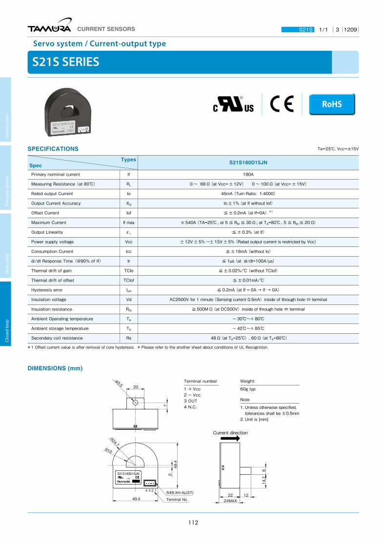
S21S SERIES
Servo system / Current-output type
Current direction
2
14.7
22 1224MAX
8
Lot No.
4 3 2 1
Terminal No.
B4B-XH-A(JST)
R10
49.4
R24.7
49.4
20
7
φ5.5
SPECIFICATIONS Ta=25℃, Vcc=±15V
TypesSpec S21S180D15JN
Primary norminal current If 180A
Measuring Resistance (at 80℃) RL 0 ~ 68Ω (at Vcc= ± 12V) 0 ~ 100Ω (at Vcc= ± 15V)
Rated output Current Io 45mA (Turn Ratio: 1:4000)
Output Current Accuracy XG Io ± 1% (at If without Iof)
Offset Current Iof ≦ ± 0.2mA (at If=0A)※1
Maximum Current If max ± 540A (TA=25℃ , at 5 ≦ RM ≦ 30Ω; at TA=80℃ , 5 ≦ RM ≦ 20Ω)
Output Linearity εL ≦ ± 0.3% (at If)
Power supply voltage Vcc ± 12V ± 5% ~± 15V ± 5% (Ratad output current is restricted by Vcc)
Consumption Current Icc ≦ ± 16mA (without Io)
di/dt Response Time(@90% of If) tr ≦ 1µs (at di/dt=100A/µs)
Thermal drift of gain TCIo ≦ ± 0.02%/℃ (without TCIof)
Thermal drift of offset TCIof ≦ ± 0.01mA/℃
Hysteresis error IoH ≦ 0.2mA (at If = 0A → If → 0A)
lnsulation voltage Vd AC2500V for 1 minute (Sensing current 0.5mA)inside of through hole ⇔ terminal
lnsulation resistance RIS ≧ 500MΩ (at DC500V)inside of through hole ⇔ terminal
Ambient Operating temperature TA ー 30℃~+ 80℃
Ambient storage temperature TS ー 40℃~+ 85℃
Secondary coil resistance Rs 48Ω (at TA=25℃), 60Ω (at TA=80℃)
*1 Offset current value is after removal of core hysteresis. * Please refer to the another sheet about conditions of UL Recognition.
DIMENSIONS (mm)
RoHS
Terminal number
1 + Vcc2 - Vcc3 OUT4 N.C.
Weight:
60g typ
Note
1. Unless otherwise specified, tolerances shall be ±0.5mm
2. Unit is [mm]
CURRENT SENSORS S21S 3 12091/1
Intr
oduc
tion
Flux
gate
sys
tem
O
pen
loop
Cl
osed
loop
112
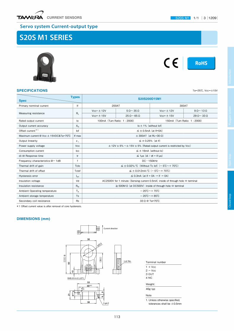
S20S M1 SERIES
Servo system Current-output type
RoHS
SPECIFICATIONS Ta=25℃, Vcc=±15V
TypesSpec S20S200D15M1
Primary norminal current If 200AT 300AT
Measuring resistance RLVcc= ± 12V 5Ω~ 35Ω Vcc= ± 12V 9Ω~ 13Ω
Vcc= ± 15V 25Ω~ 65Ω Vcc= ± 15V 29Ω~ 33Ω
Rated output current Io 100mA(Turn Ratio: 1 : 2000) 150mA(Turn Ratio: 1 : 2000)
Output current accuracy XG Io ± 1% (without Iof)
Offset current*1 Iof ≦ ± 0.5mA (at If=0A)
Maximum current @ Vcc ± 15VDC&Ta=70℃ If max ± 300AT(at RL=30Ω)
Output linearity εL ≦ ± 0.25%(at If)
Power supply voltage Vcc ± 12V ± 5% ~± 15V ± 5% (Ratad output current is restricted by Vcc)
Consumption current Icc ≦ ± 16mA (without Io)
di/dt Response time tr ≦ 1µs (di / dt = If/µs)
Frequency characteristics @- 1dB f DC…150kHz
Thermal drift of gain TcIo ≦ ± 0.02%/℃(Without Tc Iof) (ー 5℃~+ 70℃)
Thermal drift of offset TcIof ≦ ± 0.012mA/℃ (ー 5℃~+ 70℃)
Hysteresis error IoH ≦ 0.3mA (at If = 0A → If → 0A)
Insulation voltage Vd AC2500V for 1 minute (Sensing current 0.5mA) inside of through hole ⇔ terminal
Insulation resistance RIS ≧ 500MΩ (at DC500V)inside of through hole ⇔ terminal
Ambient Operating temperature TA ー 20℃~+ 70℃
Ambient storage temperature Ts ー 20℃~+ 85℃
Secondary coil resistance Rs 33Ω @ Ta=70℃
*1 Offset current value is after removal of core hysteresis.
2-φ4.2
φ20.5
R3
38
9
21
5
9
53
38
46±0.3
8±0.3
S20S200D15M1
CETA
MU
RA
1 2 34
Current direction
�3��
����
0
50
10
B4B-XH-A-G (JST)
Lot No.
DIMENSIONS (mm)
Terminal number
1 + Vcc2 - Vcc3 OUT4 NC
Weight:
46g typ
Note
1. Unless otherwise specified, tolerances shall be ±0.5mm
CURRENT SENSORS S20S M1 3 12091/1
Intr
oduc
tion
Flux
gate
sys
tem
O
pen
loop
Cl
osed
loop
113

S26P SERIES
Servo system Current-output type
14
11.5 12.7 12.7(25.4)
Lot No.
23 1 3-(0.6×0.7)
Terminal number
10.248
33.5
4.5
17
118.4 0.5
21
SPECIFICATIONS Ta=25℃, Vcc=±15V
TypesSpec
S26P200D15Y
Primary norminal current If 200A 300A
Measuring resistance @Ta=85℃ RL Vcc= ± 12V 0Ω~ 26Ω Vcc= ± 15V 0Ω~ 56Ω Vcc= ± 12V 0Ω~ 4Ω*1 Vcc= ± 15V 0Ω~ 8Ω
Rated output current Io 100mA(Turn Ratio: 1 : 2000) 150mA (Turn Ratio: 1 : 2000)
Output current accuracy XG Io ± 0.4% (Without Iof)
Offset current Iof ≦ ± 0.2mA (at If=0A)*2
Maximum currentVcc= ± 15V, Ta=85℃ If max ± 350A (at RL ≦ 5Ω)
Output linearity εL ≦ ± 0.15% (at If)
Power supply voltage Vcc ± 12V ± 5% ~± 15V ± 5% (Ratad output current is restricted by Vcc)
Consumption current Icc ≦ ± 16mA (Without Io)
di/dt Response time(@90% of If) tr ≦ 1µS (at di/dt=If/µs)
Frequency characteristics @- 1dB f DC…100kHz
Thermal drift of gain TCIo ≦ ± 0.01%/℃ (Without Tclof)
Thermal drift of offset TCIof ≦ ± 0.5mA
Hysteresis error IoH ≦ 0.3mA (at If=0A → If → If=0A)
Insulation voltage Vd AC3000V for 1 minute (Sensing current 0.5mA) inside of through hole ⇔ terminal
Insulation resistance RIS ≧ 500MΩ (at DC500V) inside of through hole ⇔ terminal
Ambient Operating temperature TA - 40℃~+ 85℃
Ambient storage temperature TS - 40℃~+ 90℃
Secondary coil resistance Rs at Ta=70℃ 60Ω at Ta=85℃ 65Ω
*1: If=250A *2 Offset current value is after removal of core hysteresis. *Please refer to the another sheet about conditions of UL Recognition.
DIMENSIONS (mm)
RoHS
Terminal number
1 + Vcc2 Output3 - Vcc
Weight:
45g typ
Note
1. Unless otherwise specified, tolerances shall be ±0.5mm
2. Unit is [mm]
CURRENT SENSORS S26P 4 12091/1
Intr
oduc
tion
Flux
gate
sys
tem
O
pen
loop
Cl
osed
loop
114

S27S SERIES
Servo system Current-output type
SPECIFICATIONS Ta=25℃, Vcc=±15V
TypesSpec S27S300D15Y S27S300D15YM
Connector ー 39-28-8040[5566-04A-210](Molex) 38-00-6293[6410-03C (102)](Molex)
Rated Current If 300A
Maximum Current RL:測定抵抗Vcc= ± 15V,Ta=85℃ If max ± 500A
Measuring resistance at Ta=85℃ If=【± ADC】 RL
± 12V 300A 0Ω~ 39Ω 500A 0Ω~ 12Ω
± 15V 300A 0Ω~ 58Ω 500A 0Ω~ 22Ω
± 20V 300A 15Ω~ 93Ω 500A 15Ω~ 45Ω
Output Current Io 150mA(Conversion Ratio 1:2000)
Output Current Accuracy XG Io ± 0.4% (without Iof)
Offset Current Iof ≦ ± 0.2mA (at If=0A)*1
Output Linearity εL ≦ ± 0.1% (at If)
Power Supply Voltage Vcc ± 12 ~± 20V
Consumption Current Icc ≦ ± 20mA (without Io)
di/dt Response Time (@90% of If) tr ≦ 1us(di/dt=100A/us)
Thermal drift of gain TCIo ≦ ± 0.01%/℃ (without Tclof)
Thermal drift of offset TCIof ≦ ± 0.5mA max
Hysteresis error IoH ≦ 0.1mA (at If = 0A → If → 0A)
lnsulation voltage Vd AC4000V, for 1minute (sensing current 0.5mA), inside of through hole ⇔ terminal
lnsulation resistance RIS ≧ 500MΩ (at DC500V)inside of through hole ⇔ terminal
Ambient Operating temperature TA ー 40℃~+ 85℃
Ambient storage temperature TS ー 40℃~+ 90℃
Secondary coil resistance Rs 25Ω(Ta=70℃) 28Ω(Ta=85℃)
*1 Offset current value is after removal of core hysteresis.* Please refer to the another sheet about conditions of UL Recognition.
RoHS
CURRENT SENSORS S27S 2 12031/2
Intr
oduc
tion
Flux
gate
sys
tem
O
pen
loop
Cl
osed
loop
115

(2.5)
(2)
5566-04A-210(Molex)
DIMENSIONS (mm)
S27S300D15Y
S27S300D15YM
Terminal number1. +Vcc2. OUT3. –Vcc
Note1. Unless otherwise specified,
tolerances shall be ±0.5mm2. Unit is [mm]
Weight: 90g typ
6860
Terminal number
1 + Vcc2 Output3 - Vcc4 nc
Weight:
90g typ
Note
1. Unless otherwise specified, tolerances shall be ±0.5mm
2. Unit is [mm]
Terminal number
1 + Vcc2 Output3 - Vcc
Weight:
90g typ
Note
1. Unless otherwise specified, tolerances shall be ±0.5mm
2. Unit is [mm]
CURRENT SENSORS S27S 2 12032/2
Intr
oduc
tion
Flux
gate
sys
tem
O
pen
loop
Cl
osed
loop
116

S28S SERIES
Servo system Current-output type
SPECIFICATIONS Ta=25℃, Vcc=±15V
TypesSpec Symbol S28S500D24Z S28S500D24ZM
Connector - 39-28-8040[5566-04A-210](Molex) 38-00-6293[6410-03C(102)](Molex)
Rated Current If 500A
Maximum Current If max ± 800A
Measuring resistance RL
± 15V 500A 0Ω~ 60Ω 800A 0Ω~ 11Ω
± 18V 500A 0Ω~ 92Ω 800A 0Ω~ 30Ω
± 24V 500A 5Ω~ 149Ω 800A 5Ω~ 65Ω
Output Current Io 100mA(Conversion Ration 1:5000)
Output Current Accuracy XG Io ± 0.5%(without Iof)
Offset Current Iof ≦± 0.4mA (at If = 0A)*1
Output Linearity εL ≦± 0.1% (at If)
Power Supply Voltage Vcc ± 15 ~± 24V
Consumption Current Icc ≦± 30mA (without Io)
di/dt Response Time (@90% of If) tr ≦ 1us(di/dt=100A/us)
Output Temperature Characteristic TCIo ≦± 0.01%/℃(Without TCIof)
Offset Temperature Characteristic TCIof ≦± 0.4mA max
Hysteresis allowance IoH ≦± 0.2mA max(at If = 0A → 3*If → 0A)
Insulation Withstanding Vd AC4,000V, for 1minute (sensing current 0.5mA) inside of through hole ⇔ terminal
Insulation Withstanding RIS ≧ 500MΩ(at DC500V)inside of through hole ⇔ terminal
Operating Temperature TA ー 40℃~+ 70℃
Storage Temperature TS ー 40℃~+ 85℃
Secondary coil resistance Rs 70Ω (Ta=70℃)
*1 Offset current value is after removal of core hysteresis.* Please refer to the another sheet about conditions of UL Recognition.
RoHS
CURRENT SENSORS S28S 1 12031/2
Intr
oduc
tion
Flux
gate
sys
tem
O
pen
loop
Cl
osed
loop
117
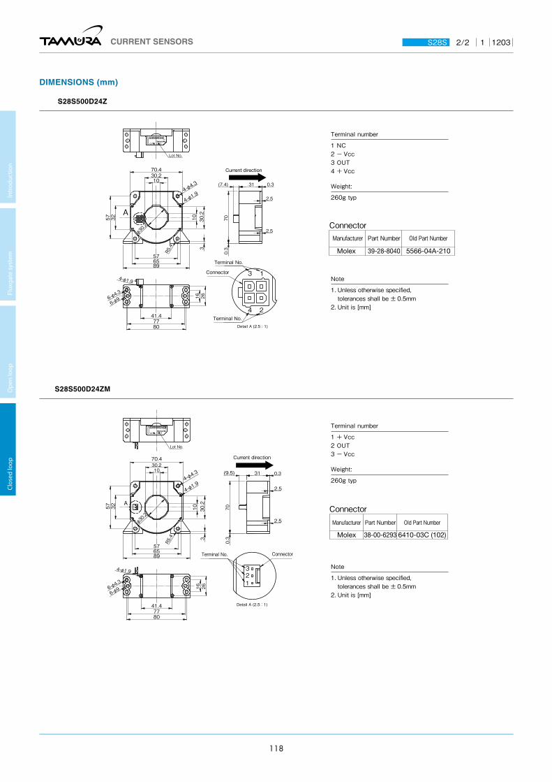
DIMENSIONS (mm)
41.4
8077
26
4-φ1.9
6-φ4.3
6-φ9 16
3257
65
4-φ4.3
4-φ1.9
57
70
0.3
2.5
31
2.5
(7.4)
0.3
Lot No.
Connector 1
24
3
Detail A (2.5 : 1)
Terminal No.
Terminal No.
Current direction
A30.2
70.4R5.4
89
10
30.210
φ30.2
3
S28S500D24Z
5566-04A-21039-28-8040
Old Part NumberPart NumberManufacturer
Connector
Molex
7780
16
41.4
6-φ4.3
6-φ9
4-φ1.9
26
32 57
57 65
4-φ4.3
4-φ1.9
Connector
321
Detail A (2.5 : 1)
Terminal No.
Current direction
A
30.2
φ30.2
89
10
30.210
3
70.4
R5.4
Lot No.
0.3
70
31
0.3
2.5
(9.5)
2.5
S28S500D24ZM
6410-03C (102)38-00-6293
Old Part NumberPart NumberManufacturer
Connector
Molex
S28S500D24Z
S28S500D24ZM
Terminal number
1 NC2 - Vcc3 OUT4 + Vcc
Weight:
260g typ
Terminal number
1 + Vcc2 OUT3 - Vcc
Weight:
260g typ
Note
1. Unless otherwise specified, tolerances shall be ± 0.5mm
2. Unit is [mm]
Note
1. Unless otherwise specified, tolerances shall be ± 0.5mm
2. Unit is [mm]
CURRENT SENSORS S28S 1 12032/2
Intr
oduc
tion
Flux
gate
sys
tem
O
pen
loop
Cl
osed
loop
118

S29S D24 SERIES
Servo system Current-output type
SPECIFICATIONS Ta=25℃, Vcc=±15V
TypesSpec Symbol S29S1T0D24Z S29S1T0D24ZM S29S1T0D24ZJ
Connector - 39-28-8040[5566-04A-210](Molex)38-00-6293 [6410-03C(102)](Molex) BH3P-VH-1(JST)
Rated current If 1000A
Maximum current 3sec If max ± 2100A
Measuring resistance RL
± 15V
70℃1000A 0Ω~ 21Ω 1200A 0Ω~ 9Ω 1300A 0Ω~ 5Ω
85℃ 1000A 0Ω~ 18Ω 1200A 0Ω~ 7Ω
± 24V
70℃1000A 0Ω~ 60.5Ω 1800A 0Ω~ 14Ω 2100A 0Ω~ 4Ω
85℃ 1000A 10Ω~ 58.5Ω 1800A 10Ω~ 12Ω
Output current Io 200mA(Conversion Ratio 1:5000)
Output current accuracy XG Io ± 0.4% (without Iof)
Offset current Iof ≦± 0.4mA(at If=0A)*1
Output linearity εL ≦± 0.1% (at If)
Power supply voltage Vcc ± 15V(± 5%)~± 24V(± 5%)
Consumption current Icc ≦± 35mA(Without Io)
di/dt response time (@90% of If) tr ≦ 1us(di/dt=100A/us)
Thermal drift of gain TCIo ≦± 0.01%/℃(without TCIof)
Thermal drift of offset TCIof ≦± 0.5mA max (at ー 10℃~+ 70℃) ≦± 0.8mA max (at ー 40℃~+ 85℃)
Hysteresis error IoH ≦± 0.2mA (at If=0A ⇒ 3×If ⇒ 0A )
Insulation withstanding Vd AC4,000V, for 1minute(sensing current 0.5mA),inside of through hole ⇔ terminal
Insulation resistance RIS ≧ 500MΩ(at DC500V)inside of through hole ⇔ terminal
Ambient Operating temperature TA ー 40℃~+ 85℃
Ambient storage temperature TS ー 40℃~+ 90℃
Secondary coil resistance Rs 48Ω(Ta=70℃) 50Ω(Ta=85℃)
*1 Offset current value is after removal of core hysteresis. *Temperature of the primary conductor(busbar) should not exceed 100℃ . *Please refer to the another sheet about conditions of UL Recognition.
RoHS
CURRENT SENSORS S29S D24 2 15081/2
Intr
oduc
tion
Flux
gate
sys
tem
O
pen
loop
Cl
osed
loop
119

DIMENSIONS (mm)
78
78
45°
R8
(47.5)
100 57
27 19
Current direction
A
38.5
8-R3
40.5 90
40.5
4-φ5.3
95
0.3
38.5
Depth:2.8
Depth:13.5±0.3
110
2-φ5.3
4-R3
4-φ2.25 4-φ4.2
4-φ3
Lot No.
0.3
3
2.5
0.3 34
7.4
3
Connector
24
13
Terminal No.
Terminal No.
Detail A (2 : 1)
78
78
45°
R8
(47.5)
19
10057
27
Current direction
A
90
95
40.5
38.5
8- R3
40.5
0.3
4-R3
110
Lot No.
0.3 3
9.5 3
2.5
34
38.5
Depth:13.5±0.3
4-φ2.25
2-φ5.3
4-φ4.2
Depth:2.84-φ3
4-φ5.3
Connector
3
Detail A (2 : 1)
21
Terminal No.
78
78
45°
(47.5)
R8
19
100 57
27
Current direction
A
40.5
40.5 90
38.5
38.5
95
0.3
8- R3
4-R3
110
Lot No.
2.5
3
0.3 3 34
10.4
Depth:2.8
Depth:13.5±0.3
4-φ2.25
2-φ5.3
4-φ4.2
4-φ3
4-φ5.3
Connector
3
2
1
Terminal No.
Detail A (2 : 1)
S29S1T0D24Z
S29S1T0D24ZM
S29S1T0D24ZJ
Terminal number
1 NC (No connection)2 +Vcc (+24V)3 ーVcc (-24V)4 Iout
Terminal number
1 +Vcc (+24V)2 Iout3 ーVcc (ー24V)
Terminal number
1 ーVcc (-24V)2 Iout3 +Vcc (+24V)
Note
1. Unless otherwise specified, tolerances shall be ±0.5mm2. Unit is [mm]
Note
1. Unless otherwise specified,
tolerances shall be ±0.5mm2. Unit is [mm]
Note
1. Unless otherwise specified, tolerances shall be ±0.5mm
2. Unit is [mm]
Weight
560g typ
Weight
560g typ
Weight
560g typ
Connector
Manufacturer Part Number Old Part Number
Molex 39-28-8040 5566-04A-210
Plating of terminal; Sn
Connector
Manufacturer Part Number Old Part Number
Molex 38-00-6293 6410-03C(102)
Plating of terminal; Sn
Connector
Manufacturer Part Number
JST BH3P-VH-1
Plating of terminal; Sn
CURRENT SENSORS S29S D24 2 15082/2
Intr
oduc
tion
Flux
gate
sys
tem
O
pen
loop
Cl
osed
loop
120
2017.4.TR
CURRENT SENSORS
SAKADO OFFICE5-5-30 Chiyoda Sakado-shi Saitama 350-0214 JapanTel : 049-284-5711 Fax : 049-284-5715
OSAKA SALES OFFICEEsaka-Sanshoubill 3-27-27 Tarumi-cho Suita-shi Osaka 564-0062 JapanTel: 06-6380-2300 Fax: 06-6385-8371
NAGOYA SALES OFFICE3-1803, Kamiyashiro, Meito-ku, Nagoya-shi, Aichi, 465-0025 JapanTel: 052-701-1210 Fax: 052-701-1295
TAMURA CORPORATION OF CHINA LIMITED13F, Block A, International Shopping Centre Shanghai No.527 Huaihai Zhong Road, Shanghai, ChinaTel : 86-21-6387-9388 Fax : 86-21-6387-9268
TAMURA ELECTRONICS(S.Z.)CO.,LTD.3014, Ban Xue Gang Street, Ban Tian Community, Ban Tian Subdistrict, Long Gang District, Shen Zhen City, ChinaTel : 86-755-8950-2603 Fax : 86-755-8950-2325
TAMURA CORPORATION OF KOREA401 Heesung building 58 Sungnae-ro Gangdong-gu Seoul S.Korea 05399Tel : 82-2-489-5354 Fax : 82-2-489-5360
TAMURA ELECTRONICS(M)SDN.BHD.Lot No.1, Jalan SS 8/6, Sungai Way Free Industrial Zone, 47300 Petaling Jaya, Selangor, MalaysiaTel : 60-3-7680-9000 Fax : 60-3-7876-3300
TAMURA CORPORATION OF AMERICA1040 South Andreasen Drive, Ste.100 Escondido, CA 92029 U.S.A.Tel : 1-951-699-1270 Fax : 1-951-676-9482
TAMURA EUROPE LIMITED.Clark Avenue Porte Marsh Industrial Estate Calne Wiltshire SN11 9BS United KingdomTEL : 44(0)-1380-731-700 FAX : 44(0)-1380-731-703
HEAD OFFICE : 1-19-43, Higashi-Oizumi, Nerima-ku, Tokyo, 178-8511 Japan http://www.tamura-ss.co.jp
Recommended