Electric breakdowns and breakdown mechanisms in ultra-thin silicon oxides
J.C. Jacksona, OÈ Oralkanb, D.J. Dumina,*, G.A. Brownc
aCenter for Semiconductor Device Reliability Research, Clemson University, Clemson, SC 29634-0915, USAbDepartment of Electrical Engineering, Stanford University, Stanford, CA 94305, USA
cTexas Instruments Inc., Dallas, TX 75265, USA
Received 30 March 1998; received in revised form 4 July 1998
Abstract
It was found that the breakdown times measured using time-dependent-dielectric-breakdown (TDDB)distributions could be shifted to shorter times when the amount of energy available during the breakdown event wasincreased. The TDDB distributions were non-unique and breakdown models must account for both electrical
breakdowns and dielectric breakdown. A novel approach for obtaining breakdown distributions will be presented.This approach uses a small number of oxides to obtain a time-dependent-electric-breakdown (TDEB) distribution,which will be shown to provide complementary information to that obtained from (TDDB) distributions. While theobservation of dielectric breakdown in ultra-thin dielectrics may be di�cult using standard test conditions, it will be
shown that electric breakdowns are relatively easy to observe. # 1999 Elsevier Science Ltd. All rights reserved.
Introduction
In order to understand the discussion of oxide
breakdown that follows, it is important to de®ne the
di�erences between electric breakdowns and thermal
breakdown. Electric breakdowns have been referred to
as soft, early, quasi, non-destructive or type A±B
breakdowns and are associated with the creation of a
temporary conducting path between the cathode and
anode. The conducting path causes a discharge of the
oxide voltage, dissipation of the oxide stored energy
through the conducting region, rapid heating of the
region to high temperatures, followed by at least par-
tial, if not full, recovery of the oxide voltage as the
breakdown region open-circuits. Many electric break-
downs are usually observed prior to a destructive, ther-
mal, dielectric breakdown. Thermal breakdown,
usually referred to as dielectric breakdown, is associ-
ated with the creation of a permanent conducting path
between the cathode and anode. Thermal or dielectric
breakdown will be shown to depend on the circuitry
used to drive the breakdown measurement.
Electric breakdowns have been known for some time
to precede destructive, thermal, dielectric breakdown
in silicon oxides [1±3]. Electric breakdowns have been
measured to occur in about a tenth of the time and at
voltages as low as half that required to produce dielec-
tric breakdown [4±9]. However, when breakdown dis-
tributions have been reported and models developed to
explain these distributions, thermal dielectric break-
downs have usually been reported and analyzed. One
reason electric breakdowns have not received much
attention in the past is because many of the break-
downs were thought to be defect related. However, the
Microelectronics Reliability 39 (1999) 171±179
0026-2714/99/$ - see front matter # 1999 Elsevier Science Ltd. All rights reserved.
PII: S0026-2714(98 )00236-4
* Corresponding author. Tel.: +1-864-656-5919; fax: +1-
864-656-5910.
E-mail address: [email protected] (D.J.
Dumin).
quality of modern oxides is so high that most of thedefect dominated breakdowns have been eliminated
and almost all breakdowns, electric and thermal, cannow be considered to be intrinsic. Recently, it has beenshown that electric breakdowns produce di�erent
breakdown distributions from thermal breakdowns,and thermal breakdown distributions are not unique[10].
In the work reported here we will describe how elec-tric breakdown distributions and thermal breakdowndistributions are di�erent. We will describe techniques
for triggering electric breakdowns into thermal break-downs. We will also describe some post-breakdowncurrent measurements that show the size of the break-down region depends on the techniques used to trigger
breakdown. A new method of extracting breakdowndistribution data will be described that uses smallersample sizes to get equivalent results to TDDB data.
Electric breakdowns in ultra-thin oxides will bedescribed. In this paper it will be shown that, while thetime-to-breakdown of electric breakdowns is di�erent
from time-to-breakdown of thermal breakdown, thereis no fundamental di�erence between an electric break-down and a thermal dielectric breakdown event, other
than one is temporary while the other is permanent.
Experimental
Electric breakdowns occur in a few microseconds
and integrating ammeters, such as the HP4140BpAmeter used for most TDDB measurements, areunable to respond to or measure electric breakdowns.
It is necessary to use a high-speed electric breakdowndetection system. The test station used to measureboth electric and thermal breakdowns reported hereused a HP4140B pAmeter to measure the oxide dc cur-
rent and voltage with a Tektronix TDS-520 digitizingstorage oscilloscope placed across the sample. Everyelectric breakdown event, the thermal breakdown
event, and the waveshape of these events were recordedin the memory of the TDS-520 or on a zip drive. Stilland video cameras were used to view and photograph
the local breakdown regions as they occurred, whichon 40 and 80 nm oxides, were easily visible under themicroscope.The oxides used in these studies were fabricated by
four separate integrated circuit manufacturers usinghigh quality LOCOS processes using both n-type andp-type substrates. Oxides with the thicknesses 1.5, 3, 4,
5, 10, 20, 40 and 80 nm were measured. Oxide areasranged from 5�10ÿ5 to 2�10ÿ3 cm2. Using custo-mized software through a general-purpose-interface-
bus (GPIB), it was possible to simultaneously apply aconstant stressing voltage, record the oxide current,record both the waveshape and time of each individual
electric breakdown during the entire stressing period ofthe oxide up to the time at which thermal breakdown
occurred, and in the thicker oxides, view and photo-graph every electric and thermal breakdown region. Itwas possible to record the waveshape associated withthe thermal breakdown. Recording of the times of
both all electric breakdowns and the thermal break-down allowed the plotting of two di�erent types ofbreakdown distributions, time-dependent-electric-
breakdown (TDEB) distributions associated with all ofthe electric breakdowns, and time-dependent-dielectric-breakdown (TDDB) distributions associated with the
®nal thermal breakdown. The measurements were allmade with the substrate in accumulation.
Electric breakdowns and dielectric breakdown
During TDDB testing, an oxide is stressed at a con-stant high electric ®eld or at a constant current densityuntil thermal dielectric breakdown is detected. The
time of the thermal breakdown is recorded when eithera precipitous increase in the current through the oxideor a drop in the voltage across the oxide occurs. The
breakdown times measured on many oxides are usedto generate a TDDB distribution. In order to record asigni®cant number of early failures a very large num-
ber of oxides must be destructively tested. With the useof the high-speed oscilloscope it is possible to recordthe times at which all electric breakdowns occur, up to
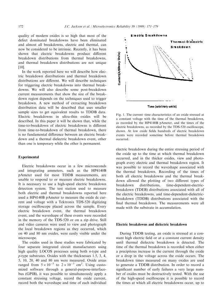
Fig. 1. The current±time characteristics of an oxide stressed at
a constant voltage with the time of the thermal breakdown,
as recorded by the HP4140B pAmeter, and the times of the
electric breakdowns, as recorded by the TDS-520 oscilloscope,
shown. At low oxide ®elds hundreds of electric breakdown
events were recorded sometime before thermal breakdown
occurred.
J.C. Jackson et al. / Microelectronics Reliability 39 (1999) 171±179172
the time of the thermal breakdown, using only a small
number of oxides. Thus, an alternative way of describ-
ing breakdown is as a series of electric breakdowns,
culminating in a ®nal, permanent, thermal, electric
breakdown, that is recorded as dielectric breakdown.
Depending on the oxide ®eld, hundreds of electric
breakdowns can occur prior to thermal breakdown. It
will be shown that in oxides thinner than about 5 nm,
where the stored energy in the oxide is small and
detection of thermal breakdown is di�cult, electric
breakdowns are an easier technique for detecting
breakdown. In Fig. 1 a typical current±time character-
istic measured during a constant-voltage TDDB
measurement is shown. Both the time at which the
thermal breakdown occurred, as recorded on the
HP4140B pAmeter, and the times at which electric
breakdowns occurred, as recorded by the TDS-520,
have been shown.
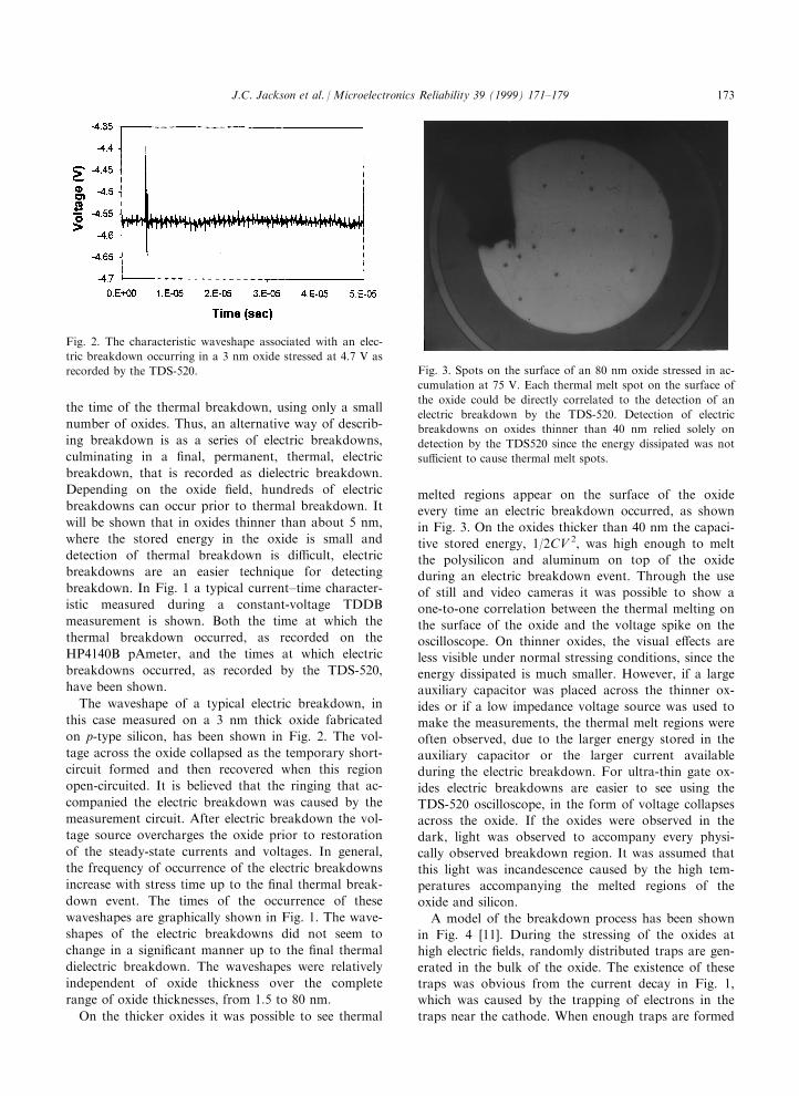
The waveshape of a typical electric breakdown, in
this case measured on a 3 nm thick oxide fabricated
on p-type silicon, has been shown in Fig. 2. The vol-
tage across the oxide collapsed as the temporary short-
circuit formed and then recovered when this region
open-circuited. It is believed that the ringing that ac-
companied the electric breakdown was caused by the
measurement circuit. After electric breakdown the vol-
tage source overcharges the oxide prior to restoration
of the steady-state currents and voltages. In general,
the frequency of occurrence of the electric breakdowns
increase with stress time up to the ®nal thermal break-
down event. The times of the occurrence of these
waveshapes are graphically shown in Fig. 1. The wave-
shapes of the electric breakdowns did not seem to
change in a signi®cant manner up to the ®nal thermal
dielectric breakdown. The waveshapes were relatively
independent of oxide thickness over the complete
range of oxide thicknesses, from 1.5 to 80 nm.
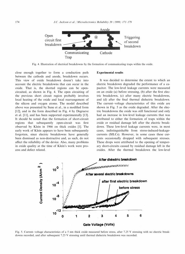
On the thicker oxides it was possible to see thermal
melted regions appear on the surface of the oxide
every time an electric breakdown occurred, as shown
in Fig. 3. On the oxides thicker than 40 nm the capaci-
tive stored energy, 1/2CV 2, was high enough to melt
the polysilicon and aluminum on top of the oxide
during an electric breakdown event. Through the use
of still and video cameras it was possible to show a
one-to-one correlation between the thermal melting on
the surface of the oxide and the voltage spike on the
oscilloscope. On thinner oxides, the visual e�ects are
less visible under normal stressing conditions, since the
energy dissipated is much smaller. However, if a large
auxiliary capacitor was placed across the thinner ox-
ides or if a low impedance voltage source was used to
make the measurements, the thermal melt regions were
often observed, due to the larger energy stored in the
auxiliary capacitor or the larger current available
during the electric breakdown. For ultra-thin gate ox-
ides electric breakdowns are easier to see using the
TDS-520 oscilloscope, in the form of voltage collapses
across the oxide. If the oxides were observed in the
dark, light was observed to accompany every physi-
cally observed breakdown region. It was assumed that
this light was incandescence caused by the high tem-
peratures accompanying the melted regions of the
oxide and silicon.
A model of the breakdown process has been shown
in Fig. 4 [11]. During the stressing of the oxides at
high electric ®elds, randomly distributed traps are gen-
erated in the bulk of the oxide. The existence of these
traps was obvious from the current decay in Fig. 1,
which was caused by the trapping of electrons in the
traps near the cathode. When enough traps are formed
Fig. 2. The characteristic waveshape associated with an elec-
tric breakdown occurring in a 3 nm oxide stressed at 4.7 V as
recorded by the TDS-520. Fig. 3. Spots on the surface of an 80 nm oxide stressed in ac-
cumulation at 75 V. Each thermal melt spot on the surface of
the oxide could be directly correlated to the detection of an
electric breakdown by the TDS-520. Detection of electric
breakdowns on oxides thinner than 40 nm relied solely on
detection by the TDS520 since the energy dissipated was not
su�cient to cause thermal melt spots.
J.C. Jackson et al. / Microelectronics Reliability 39 (1999) 171±179 173
close enough together to form a conduction path
between the cathode and anode, breakdown occurs.
This view of oxide breakdown doesn't take into
account the electric breakdowns that can occur in the
oxide. That is, the shorted regions can be open-
circuited, as shown in Fig. 4. The open circuiting of
the previous short circuit region probably involves
local heating of the oxide and local rearrangement of
the silicon and oxygen atoms. The model described
above was presented by Sune et al., in a modi®ed form
[12], and in the form described in Fig. 4 by Degraeve
et al. [11], and has been supported experimentally [13].
It should be noted that the formation of short-circuit
regions that subsequently open-circuit was ®rst
observed by Klein in 1966 on thick oxides [1]. The
early work of Klein appears to have been subsequently
forgotten, since electric breakdowns have generally
been dismissed as non-destructive and, as such, do not
a�ect the reliability of the device. Also, many problems
in oxide quality at the time of Klein's work were pro-
cess and defect related.
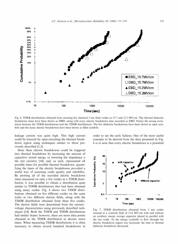
Experimental results
It was decided to determine the extent to which an
electric breakdown degraded the performance of a ca-
pacitor. The low-level leakage currents were measured
on an oxide (a) before stressing, (b) after the ®rst elec-
tric breakdown, (c) after many electric breakdowns,
and (d) after the ®nal thermal dielectric breakdown.
The current±voltage characteristics of this oxide are
shown in Fig. 5 as the oxide degraded. After the elec-
tric breakdowns the oxide was still functional and only
had an increase in low-level leakage currents that was
attributed to either the formation of traps within the
oxide or residual damage left after the electric break-
down. These low-level leakage currents were, in most
cases, indistinguishable from stress-induced-leakage-
currents (SILCs). However, in some cases these cur-
rents occasionally dropped with subsequent stresses.
These drops were attributed to the opening of tempor-
ary short-circuits caused by residual damage left in the
oxides. After the thermal breakdown the low-level
Fig. 4. Illustration of electrical breakdowns by the formation of communicating traps within the oxide.
Fig. 5. Current±voltage characteristics of a 5 nm thick oxide measured before stress, after 7.25 V stressing with no electric break-
downs recorded, and after subsequent 7.25 V stressing until thermal dielectric breakdown was recorded.
J.C. Jackson et al. / Microelectronics Reliability 39 (1999) 171±179174
leakage current was quite high. This high current
could be lowered by open-circuiting the thermal break-
down region using techniques similar to those pre-
viously described [1,3].
Since these electric breakdowns could be triggered
into thermal breakdown by increasing the amount of
capacitive stored energy or lowering the impedance o
the test circuitry [10], and, as such, represented all
possible times for possible thermal breakdown, quanti-
fying the times of the electric breakdowns provided a
useful way of accessing oxide quality and reliability.
By plotting all of the recorded electric breakdown
times measured on only a few oxides in a TDEB distri-
bution, it was possible to obtain a distribution quite
similar to TDDB distributions that had been obtained
using many oxides. Fig. 6 shows two TDEB distri-
butions obtained on ®ve di�erent oxides on the same
wafer at two di�erent electric ®elds, along with the
TDDB distribution obtained from these ®ve oxides.
The electric ®elds were determined from the current±
voltage characteristics using previously described tech-
niques [14]. Both the TDEB and TDDB distributions
had similar slopes; however, there are more data points
obtained in the TDEB distribution at shorter stress
times. When measuring TDDB distributions it is often
necessary to obtain several hundred breakdowns in
order to see the early failures. One of the most useful
concepts to be derived from the data presented in Fig.
6 is to note that every electric breakdown is a potential
Fig. 6. TDEB distributions obtained from stressing ®ve identical 3 nm thick oxides at 15.7 and 15.2 MV/cm. The thermal dielectric
breakdown times have been shown as DBD, along with every electric breakdown time recorded as EBD. Notice the strong corre-
lation between the TDEB distributions and the TDDB distributions. The ®ve dielectric breakdowns have been shown as open sym-
bols and the many electric breakdowns have been shown as ®lled symbols.
Fig. 7. TDEB distributions obtained from 3 nm oxides
stressed at a constant ®eld of 15.6 MV/cm with and without
an auxiliary energy storage capacitor placed in parallel with
the test oxide. As the energy available to ¯ow through the
electric breakdown region was increased, the time to thermal
dielectric breakdown decreased.
J.C. Jackson et al. / Microelectronics Reliability 39 (1999) 171±179 175
thermal dielectric breakdown. If the local conditions in
the oxide and the driving circuitry are matched, then
an electric breakdown can be triggered into a thermal
breakdown. Since there were often hundreds of electricbreakdowns occurring during an electric breakdown
test and every possible breakdown was recorded, it
was found that in many cases the TDEB distributions
were multi-modal. Multi-modal TDDB distributions
were usually only obtained when many hundreds of
oxides were destructively measured.
In previous work we have shown that, on thicker
oxides, it was possible to shift the time of the dielectric
breakdown to shorter times (a) by increasing the ca-
pacitive energy available to discharge during an electric
breakdown, or (b) by using a low impedance voltage
source [10]. Similar experiments were conducted on ox-
ides as thin as 3 nm. Two TDEB distributions
obtained on 3 nm thick oxides have been shown in
Fig. 7. One of the distributions was obtained from theoxides and one of the distributions was obtained from
the oxides that had the additional 330 mF capacitor
placed in parallel with the test oxide. The TDEB distri-
bution obtained with the parallel capacitor was shifted
to shorter breakdown times. It is important to note
that the electric breakdowns recorded under both con-
ditions began at approximately the same time and only
the ®nal thermal dielectric breakdowns were di�erent.
The multi-modal nature of the TDEB distribution isclearly seen in these data. In order to obtain a similar
measurement using TDDB testing, several hundred
breakdowns would have been needed.
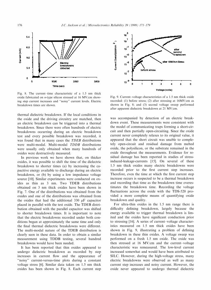
It has been reported that thin oxides appeared to
undergo dielectric breakdown as recorded by stepincreases in current ¯ow and the appearance of
``noisy'' current-versus-time plots during a constant
voltage stress [6]. Similar data taken on 1.5 nm thick
oxides has been shown in Fig. 8. Each current step
was accompanied by detection of an electric break-
down event. These measurements were consistent with
the model of communicating traps forming a short-cir-
cuit and then partially open-circuiting. Since the oxide
current never completely relaxes to its original value, it
appeared that the short circuit was unable to comple-
tely open-circuit and residual damage from melted
oxide, the polysilicon, or the substrate remained in the
oxide throughout the measurements. Evidence for re-
sidual damage has been reported in studies of stress-
induced-leakage-currents [15]. On several of these
1.5 nm thick oxides many electric breakdowns were
recorded prior to the ®rst current step increases.
Therefore, even the time at which the ®rst current step
increase occurs is suspected to be a thermal breakdown
and recording that time as the breakdown time overes-
timates the breakdown time. Recording the voltage
¯uctuations across the oxide with the TDS-520 pro-
vided a more complete means of quantifying oxide
breakdown and quality.
For ultra-thin oxides in the 1.5 nm range there is
di�culty de®ning breakdown, largely because the
energy available to trigger thermal breakdown is lim-
ited and the oxides have signi®cant conduction prior
to stressing [16]. A series of current±voltage character-
istics measured on 1.5 nm thick oxides have been
shown in Fig. 9, illustrating a problem of de®ning
breakdown in these thin oxides. A voltage sweep was
performed on a fresh 1.5 nm oxide. The oxide was
then stressed at 16 MV/cm and the current±voltage
characteristic was remeasured. The low-level current
increased somewhat and would have been attributed to
SILC. However, during the high-voltage stress, many
electric breakdowns were observed as well as many
current step increases and noisy current. However, the
oxide never appeared to undergo thermal dielectric
Fig. 8. The current±time characteristic of a 1.5 nm thick
oxide fabricated on n-type silicon stressed at 16 MV/cm show-
ing step current increases and ``noisy'' current levels. Electric
breakdown times are shown.
Fig. 9. Current±voltage characteristics of a 1.5 nm thick oxide
recorded: (1) before stress; (2) after stressing at 16MV/cm as
shown in Fig. 8; and (3) second voltage sweep performed
after apparent dielectric breakdown at 21 MV/cm.
J.C. Jackson et al. / Microelectronics Reliability 39 (1999) 171±179176
breakdown. The increased SILC was probably due
both to trap generation and residual damage inside the
oxide. As the voltage was swept to higher ®elds, the
oxide appeared to undergo a second breakdown, as
indicated by the jump in the current that occurred at
voltages above 3.3 V. A subsequent voltage sweep con-
®rmed that a very low resistance shorting path had
formed between the cathode and anode. Thus, this
oxide might not have been described as having under-
gone breakdown after the ®rst stress, when in fact,
many electric breakdowns were measured. These
results are consistent with the recent paper at IEDM
in which the oxides in the 2 nm range never appeared
to undergo dielectric breakdown [16]. However, since
electric breakdowns still occur, measurement of the
electric breakdown times provide a convenient means
of quantifying breakdown in ultra-thin oxides.
Since the dielectric breakdown event in an oxide is
largely dominated by thermal events, changing the
amount of energy that is available for discharge
through a shorting path should cause the temperature
of this path to vary and should produce varying ®nal
states of the oxide. Since the ®nal state of the oxide
depends on the details of the triggering of breakdown
and maintaining the current though the breakdown
region, the complexity of de®ning the true dielectric
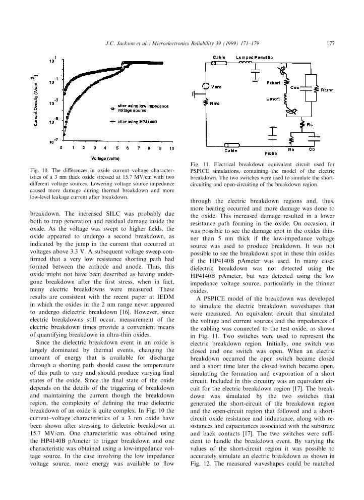
breakdown of an oxide is quite complex. In Fig. 10 the
current±voltage characteristics of a 3 nm oxide have
been shown after stressing to dielectric breakdown at
15.7 MV/cm. One characteristic was obtained using
the HP4140B pAmeter to trigger breakdown and one
characteristic was obtained using a low-impedance vol-
tage source. In the case involving the low impedance
voltage source, more energy was available to ¯ow
through the electric breakdown regions and, thus,
more heating occurred and more damage was done to
the oxide. This increased damage resulted in a lower
resistance path forming in the oxide. On occasion, it
was possible to see the damage spot in the oxides thin-
ner than 5 nm thick if the low-impedance voltage
source was used to produce breakdown. It was not
possible to see the breakdown spot in these thin oxides
if the HP4140B pAmeter was used. In many cases
dielectric breakdown was not detected using the
HP4140B pAmeter, but was detected using the low
impedance voltage source, particularly in the thinner
oxides.
A PSPICE model of the breakdown was developed
to simulate the electric breakdown waveshapes that
were measured. An equivalent circuit that simulated
the voltage and current sources and the impedances of
the cabling was connected to the test oxide, as shown
in Fig. 11. Two switches were used to represent the
electric breakdown region. Initially, one switch was
closed and one switch was open. When an electric
breakdown occurred the open switch became closed
and a short time later the closed switch became open,
simulating the formation and evaporation of a short
circuit. Included in this circuitry was an equivalent cir-
cuit for the electric breakdown region [17]. The break-
down was simulated by the two switches that
generated the short-circuit of the breakdown region
and the open-circuit region that followed and a short-
circuit oxide resistance and inductance, along with re-
sistances and capacitances associated with the substrate
and back contacts [17]. The two switches were su�-
cient to handle the breakdown event. By varying the
values of the short-circuit region it was possible to
accurately simulate an electric breakdown as shown in
Fig. 12. The measured waveshapes could be matched
Fig. 10. The di�erences in oxide current±voltage character-
istics of a 3 nm thick oxide stressed at 15.7 MV/cm with two
di�erent voltage sources. Lowering voltage source impedance
caused more damage during thermal breakdown and more
low-level leakage current after breakdown.
Fig. 11. Electrical breakdown equivalent circuit used for
PSPICE simulations, containing the model of the electric
breakdown. The two switches were used to simulate the short-
circuiting and open-circuiting of the breakdown region.
J.C. Jackson et al. / Microelectronics Reliability 39 (1999) 171±179 177
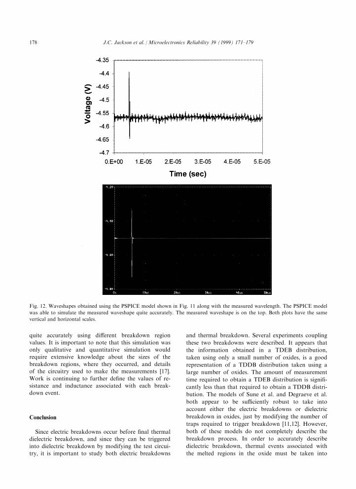
quite accurately using di�erent breakdown regionvalues. It is important to note that this simulation wasonly qualitative and quantitative simulation would
require extensive knowledge about the sizes of thebreakdown regions, where they occurred, and detailsof the circuitry used to make the measurements [17].
Work is continuing to further de®ne the values of re-sistance and inductance associated with each break-down event.
Conclusion
Since electric breakdowns occur before ®nal thermal
dielectric breakdown, and since they can be triggeredinto dielectric breakdown by modifying the test circui-try, it is important to study both electric breakdowns
and thermal breakdown. Several experiments coupling
these two breakdowns were described. It appears that
the information obtained in a TDEB distribution,
taken using only a small number of oxides, is a good
representation of a TDDB distribution taken using a
large number of oxides. The amount of measurement
time required to obtain a TDEB distribution is signi®-
cantly less than that required to obtain a TDDB distri-
bution. The models of Sune et al. and Degraeve et al.
both appear to be su�ciently robust to take into
account either the electric breakdowns or dielectric
breakdown in oxides, just by modifying the number of
traps required to trigger breakdown [11,12]. However,
both of these models do not completely describe the
breakdown process. In order to accurately describe
dielectric breakdown, thermal events associated with
the melted regions in the oxide must be taken into
Fig. 12. Waveshapes obtained using the PSPICE model shown in Fig. 11 along with the measured wavelength. The PSPICE model
was able to simulate the measured waveshape quite accurately. The measured waveshape is on the top. Both plots have the same
vertical and horizontal scales.
J.C. Jackson et al. / Microelectronics Reliability 39 (1999) 171±179178
account. The TDEB distributions de®ne all the poss-ible times for oxide failure. The TDDB distribution
only provides the time of the ®nal failure. Every elec-tric breakdown is a possible dielectric breakdown.Whether this electric breakdown becomes a thermal
breakdown is often determined by the test circuitry,and not the oxide itself. For ultra-thin gate oxides the®nal state of the oxide after breakdown is dependent
on the test conditions present during an electric break-down. We believe that TDEB distributions provide amethod of looking at early failures within an oxide
and are a good complement to or even a replacementfor the TDDB distribution.
References
[1] Klein N. IEEE Trans Electron Devices 1966;ED-13:788.
[2] Shatzkes M, et al. J Appl Phys 1974;45:2065.
[3] Solomon P. J Vac Sci Technol 1977;14:1122.
[4] Shatzkes M, Av-Ron M. 1992 IEEE/IRPS Tutorial no.
6.
[5] Neri B, et al. Appl Phys Lett 1987;51:2167.
[6] Farmer KR, et al. Appl Phys Lett 1988;52:1749.
[7] Yoshida T, et al. International Conference on Solid State
Devices and Materials, 1996.
[8] Satake H, et al. Appl Phys Lett 1996;69:1128.
[9] Depas M, et al. IEEE Trans Electron Devices 1996;ED-
43:1499.
[10] Jackson JC, et al. Appl Phys Lett 1997;71.
[11] Degraeve R, et al. Proceedings of IEDM, 1995. p. 863.
[12] Sune J, et al. Thin Film Solids 1990;185:347.
[13] Dumin DJ, et al. IEEE Trans Electron Devices 1994;ED-
41:1570.
[14] Ashton RA. Proceedings of International Conference on
Microelectronic Test Structures, 1991. 4. p. 57.
[15] Okada K. Exerted Abstracts of the 1996 International
Conference on Solid State Devices and Materials, 26±29
August, Yokohama, Japan, 1996. p. 782.
[16] Weir BE, et al. Proceedings of IEDM, 1997. p. 73.
[17] Bridgewood MA, et al. Electrical Overstress/Electrostatic
Discharge Symposium Proceedings, 1985. p. 84.
J.C. Jackson et al. / Microelectronics Reliability 39 (1999) 171±179 179
Recommended