1246 IEEE TRANSACTIONS ON VERY LARGE SCALE INTEGRATION (VLSI) SYSTEMS, VOL. 21, NO. 7, JULY 2013
Efficient Vector Graphics Rasterization AcceleratorUsing Optimized Scan-Line Buffer
Ting-Chi Tong and Yun-Nan Chang
Abstract— This paper presents a small and fast VLSI archi-tecture of a vector graphics rasterization accelerator. To decidethe filling regions of a graphics object, a large on-chip scan-line buffer (SB) is very often used and frequently accessed toderive the pixel’s winding count. This paper, first, proposes aspecial 2-bit coding scheme for buffer entry along with active-edge-table rescan to record the intersection information of scanlines and the object paths. Second, for AA rendering applications,a coverage buffer is proposed to avoid the duplication of SBs.Compared with the conventional approach, the required buffersize can be reduced by up to 89%. Besides buffer reduction,this paper also proposes a hierarchical SB architecture in whichthe upper-level buffer indicates which scan-line sections haveintersected with objects in order to skip the access to successivebuffer entries. The same technique, along with the differentialcoverage transformation, can also be applied to coverage buffer.Our experimental results show that more than 87% of memoryaccesses can be reduced, which results in saving 66.4% of clockcycles in practical hardware implementation. The gate count ofthe proposed rasterization accelerator is only about 32 232, andcan run at 250 MHz under UMC 90-nm technology for HDTVapplications.
Index Terms— 2-D graphics, anti-aliasing (AA), OpenVG,rasterization, scan-line buffer (SB), vector graphics.
I. INTRODUCTION
VECTOR graphics applications have been widely used invarious consumer electronic devices such as electronic
books, electronic maps, and mobile phones. In contrast tobitmap graphics, vector graphics uses mathematical equationsto describe objects such that the amount of data representingthe objects can be reduced. By evaluating the mathematicalequations according to the given screen resolution, the objectscan be rendered without losing image quality. Therefore, vec-tor graphics is very suitable for devices with limited memorycapacity, such as embedded systems or image viewers withzoom-in or zoom-out capability such as smart phones.
While more and more products equipped with vector graph-ics applications are developed by different manufacturers, astandard for vector graphics needs to be complied with inorder to make applications compatible at diverse platforms.SVG [1] and OpenVG [2] are the two most popular vector
Manuscript received December 27, 2011; revised April 21, 2012; acceptedJune 12, 2012. Date of publication August 9, 2012; date of current versionJune 21, 2013. This work was supported in part by the National ScienceCouncil of Taiwan under Grant NSC 100-2221-E-110-053-MY3.
The authors are with the Department of Computer Science and Engineer-ing, National Sun Yat-Sen University, Kaohsiung 80424, Taiwan (e-mail:[email protected]; [email protected]).
Color versions of one or more of the figures in this paper are availableonline at http://ieeexplore.ieee.org.
Digital Object Identifier 10.1109/TVLSI.2012.2207413
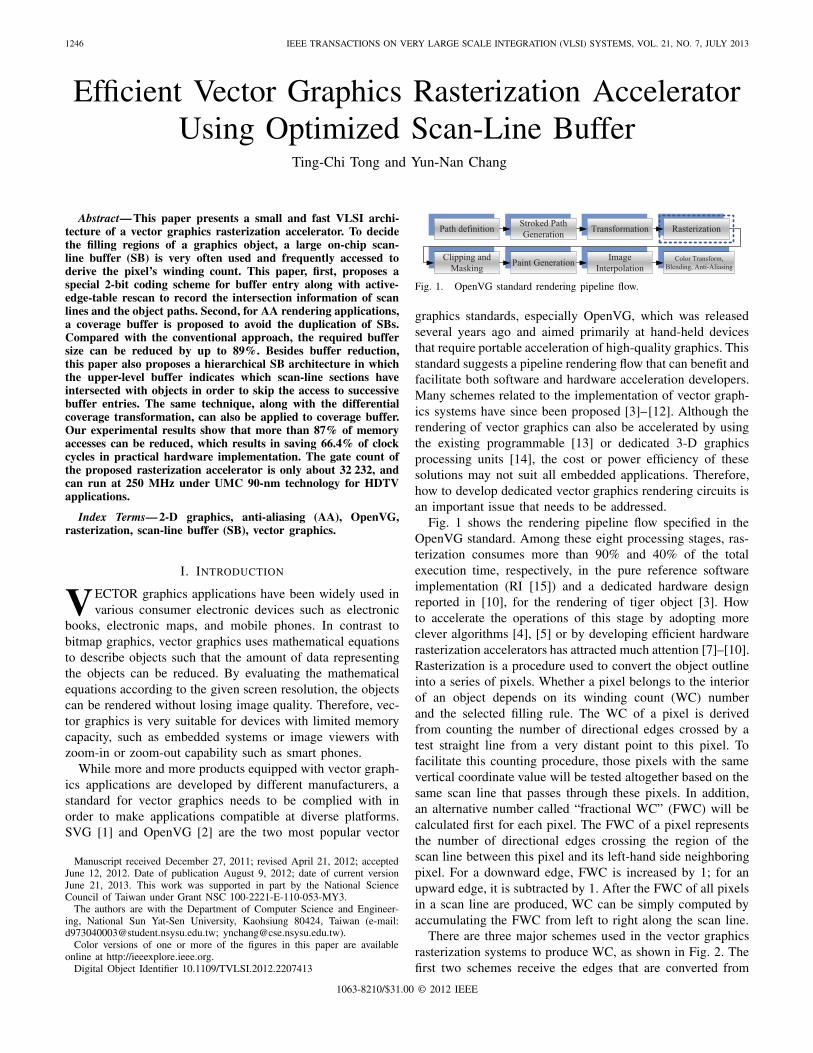
Fig. 1. OpenVG standard rendering pipeline flow.
graphics standards, especially OpenVG, which was releasedseveral years ago and aimed primarily at hand-held devicesthat require portable acceleration of high-quality graphics. Thisstandard suggests a pipeline rendering flow that can benefit andfacilitate both software and hardware acceleration developers.Many schemes related to the implementation of vector graph-ics systems have since been proposed [3]–[12]. Although therendering of vector graphics can also be accelerated by usingthe existing programmable [13] or dedicated 3-D graphicsprocessing units [14], the cost or power efficiency of thesesolutions may not suit all embedded applications. Therefore,how to develop dedicated vector graphics rendering circuits isan important issue that needs to be addressed.
Fig. 1 shows the rendering pipeline flow specified in theOpenVG standard. Among these eight processing stages, ras-terization consumes more than 90% and 40% of the totalexecution time, respectively, in the pure reference softwareimplementation (RI [15]) and a dedicated hardware designreported in [10], for the rendering of tiger object [3]. Howto accelerate the operations of this stage by adopting moreclever algorithms [4], [5] or by developing efficient hardwarerasterization accelerators has attracted much attention [7]–[10].Rasterization is a procedure used to convert the object outlineinto a series of pixels. Whether a pixel belongs to the interiorof an object depends on its winding count (WC) numberand the selected filling rule. The WC of a pixel is derivedfrom counting the number of directional edges crossed by atest straight line from a very distant point to this pixel. Tofacilitate this counting procedure, those pixels with the samevertical coordinate value will be tested altogether based on thesame scan line that passes through these pixels. In addition,an alternative number called “fractional WC” (FWC) will becalculated first for each pixel. The FWC of a pixel representsthe number of directional edges crossing the region of thescan line between this pixel and its left-hand side neighboringpixel. For a downward edge, FWC is increased by 1; for anupward edge, it is subtracted by 1. After the FWC of all pixelsin a scan line are produced, WC can be simply computed byaccumulating the FWC from left to right along the scan line.
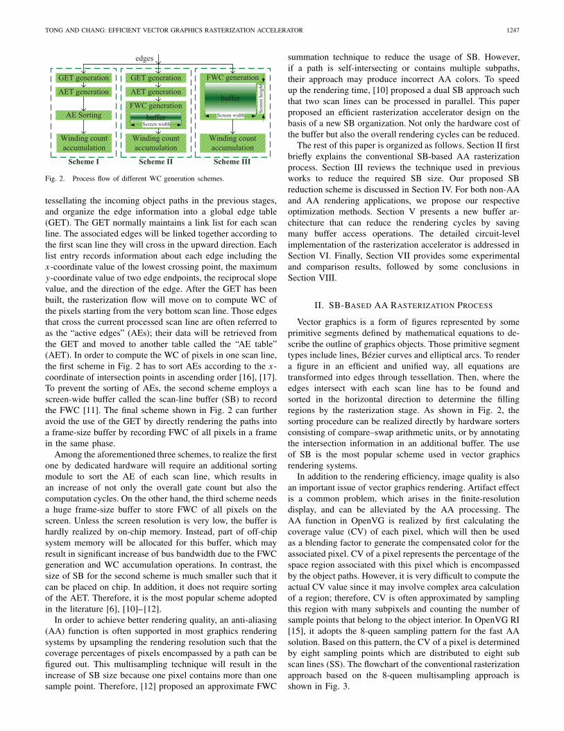
There are three major schemes used in the vector graphicsrasterization systems to produce WC, as shown in Fig. 2. Thefirst two schemes receive the edges that are converted from
1063-8210/$31.00 © 2012 IEEE
TONG AND CHANG: EFFICIENT VECTOR GRAPHICS RASTERIZATION ACCELERATOR 1247
Fig. 2. Process flow of different WC generation schemes.
tessellating the incoming object paths in the previous stages,and organize the edge information into a global edge table(GET). The GET normally maintains a link list for each scanline. The associated edges will be linked together according tothe first scan line they will cross in the upward direction. Eachlist entry records information about each edge including thex-coordinate value of the lowest crossing point, the maximumy-coordinate value of two edge endpoints, the reciprocal slopevalue, and the direction of the edge. After the GET has beenbuilt, the rasterization flow will move on to compute WC ofthe pixels starting from the very bottom scan line. Those edgesthat cross the current processed scan line are often referred toas the “active edges” (AEs); their data will be retrieved fromthe GET and moved to another table called the “AE table”(AET). In order to compute the WC of pixels in one scan line,the first scheme in Fig. 2 has to sort AEs according to the x-coordinate of intersection points in ascending order [16], [17].To prevent the sorting of AEs, the second scheme employs ascreen-wide buffer called the scan-line buffer (SB) to recordthe FWC [11]. The final scheme shown in Fig. 2 can furtheravoid the use of the GET by directly rendering the paths intoa frame-size buffer by recording FWC of all pixels in a framein the same phase.
Among the aforementioned three schemes, to realize the firstone by dedicated hardware will require an additional sortingmodule to sort the AE of each scan line, which results inan increase of not only the overall gate count but also thecomputation cycles. On the other hand, the third scheme needsa huge frame-size buffer to store FWC of all pixels on thescreen. Unless the screen resolution is very low, the buffer ishardly realized by on-chip memory. Instead, part of off-chipsystem memory will be allocated for this buffer, which mayresult in significant increase of bus bandwidth due to the FWCgeneration and WC accumulation operations. In contrast, thesize of SB for the second scheme is much smaller such that itcan be placed on chip. In addition, it does not require sortingof the AET. Therefore, it is the most popular scheme adoptedin the literature [6], [10]–[12].
In order to achieve better rendering quality, an anti-aliasing(AA) function is often supported in most graphics renderingsystems by upsampling the rendering resolution such that thecoverage percentages of pixels encompassed by a path can befigured out. This multisampling technique will result in theincrease of SB size because one pixel contains more than onesample point. Therefore, [12] proposed an approximate FWC
summation technique to reduce the usage of SB. However,if a path is self-intersecting or contains multiple subpaths,their approach may produce incorrect AA colors. To speedup the rendering time, [10] proposed a dual SB approach suchthat two scan lines can be processed in parallel. This paperproposed an efficient rasterization accelerator design on thebasis of a new SB organization. Not only the hardware cost ofthe buffer but also the overall rendering cycles can be reduced.
The rest of this paper is organized as follows. Section II firstbriefly explains the conventional SB-based AA rasterizationprocess. Section III reviews the technique used in previousworks to reduce the required SB size. Our proposed SBreduction scheme is discussed in Section IV. For both non-AAand AA rendering applications, we propose our respectiveoptimization methods. Section V presents a new buffer ar-chitecture that can reduce the rendering cycles by savingmany buffer access operations. The detailed circuit-levelimplementation of the rasterization accelerator is addressed inSection VI. Finally, Section VII provides some experimentaland comparison results, followed by some conclusions inSection VIII.
II. SB-BASED AA RASTERIZATION PROCESS
Vector graphics is a form of figures represented by someprimitive segments defined by mathematical equations to de-scribe the outline of graphics objects. Those primitive segmenttypes include lines, Bézier curves and elliptical arcs. To rendera figure in an efficient and unified way, all equations aretransformed into edges through tessellation. Then, where theedges intersect with each scan line has to be found andsorted in the horizontal direction to determine the fillingregions by the rasterization stage. As shown in Fig. 2, thesorting procedure can be realized directly by hardware sortersconsisting of compare–swap arithmetic units, or by annotatingthe intersection information in an additional buffer. The useof SB is the most popular scheme used in vector graphicsrendering systems.
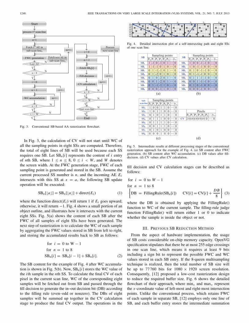
In addition to the rendering efficiency, image quality is alsoan important issue of vector graphics rendering. Artifact effectis a common problem, which arises in the finite-resolutiondisplay, and can be alleviated by the AA processing. TheAA function in OpenVG is realized by first calculating thecoverage value (CV) of each pixel, which will then be usedas a blending factor to generate the compensated color for theassociated pixel. CV of a pixel represents the percentage of thespace region associated with this pixel which is encompassedby the object paths. However, it is very difficult to compute theactual CV value since it may involve complex area calculationof a region; therefore, CV is often approximated by samplingthis region with many subpixels and counting the number ofsample points that belong to the object interior. In OpenVG RI[15], it adopts the 8-queen sampling pattern for the fast AAsolution. Based on this pattern, the CV of a pixel is determinedby eight sampling points which are distributed to eight subscan lines (SS). The flowchart of the conventional rasterizationapproach based on the 8-queen multisampling approach isshown in Fig. 3.
1248 IEEE TRANSACTIONS ON VERY LARGE SCALE INTEGRATION (VLSI) SYSTEMS, VOL. 21, NO. 7, JULY 2013
Fig. 3. Conventional SB-based AA rasterization flowchart.
In Fig. 3, the calculation of CV will not start until WC ofall the sampling points in eight SSs are computed. Therefore,the total of eight lines of SB will be used because each SSrequires one SB. Let SBn[i ] represents the content of i entryof nth SB, where 1 ≤ n ≤ 8, 0 ≤ i < W , and W denotesthe screen width. At the FWC generation stage, FWC of eachsampling point is generated and stored in the SB. Assume thecurrent processed SS number is n, and the incoming AE Ei
intersects with this SS at x = a, the following SB updateoperation will be executed:
SBn[�a�] = SBn[�a�] + direct(Ei ) (1)
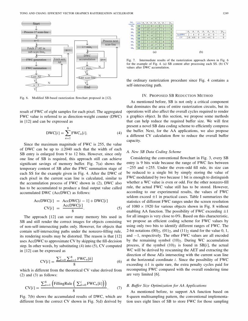
where the function direct(Ei ) will return 1 if Ei goes upward;otherwise, it will return −1. Fig. 4 shows a small portion of anobject outline, and illustrates how it intersects with the currenteight SSs. Fig. 5(a) shows the content of each SB after theFWC of all samples of eight SSs have been generated. Thenext step of rasterization is to calculate the WC of each sampleby aggregating the FWC values stored in SB from left to right,and storing the accumulated results back to SB as follows:
for i = 0 to W − 1
for n = 1 to 8
SBn[i ] = SBn[i − 1] + SBn[i ]. (2)
The SB content for the example of Fig. 4 after WC accumula-tion is shown in Fig. 5(b). Now, SBn[i ] stores the WC value ofthe i th sample in the nth SS. To calculate the final CV of eachpixel in the current scan line, WC of the corresponding eightsamples will be fetched out from SB and passed through thefill decision to generate the in–out decision bit (DB) accordingto the filling rule (even–odd or nonzero). The DBs of eightsamples will be summed up together in the CV calculationstage to produce the final CV output. The operations in the
Fig. 4. Detailed intersection plot of a self-intersecting path and eight SSsof one scan line.
Fig. 5. Intermediate results at different processing stages of the conventionalrasterization approach for the example of Fig. 4. (a) SB content after FWCgeneration. (b) SB content after WC accumulation. (c) DB values after fill-decision. (d) CV values after CV calculation.
fill decision and CV calculation stages can be described asfollows:for i = 0 to W − 1
for n = 1 to 8{DB = FillingRule(SBn[i ]) CV[i ] = CV[i ] + DB
8
}(3)
where the DB is obtained by applying the FillingRule()function to WC of the current sample. The filling-rule judgefunction FillingRule() will return either 1 or 0 to indicatewhether the sample is inside the object or not.
III. PREVIOUS SB REDUCTION METHOD
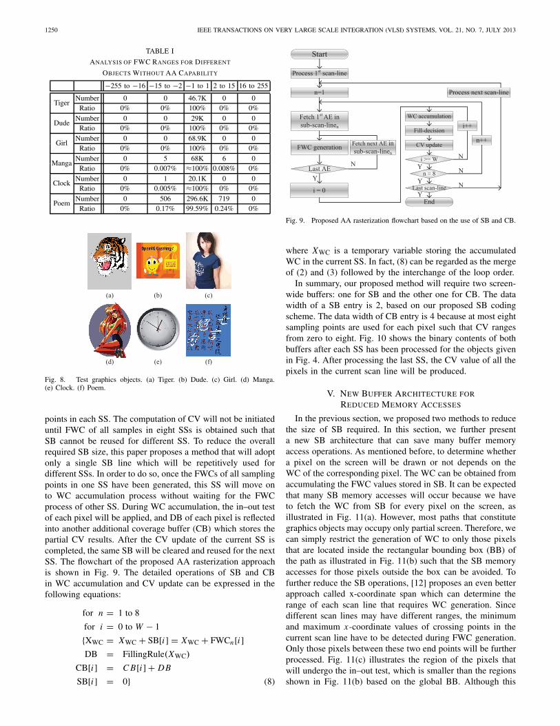
From the aspect of hardware implementation, the usageof SB costs considerable on-chip memory capacity. OpenVGspecification stipulates that there be at most 255 edge crossingsin one scan line, which means it requires at least 9 bitsincluding a sign bit to represent the possible FWC and WCvalues stored in each SB entry. If the 8-queen multisamplingtechnique is realized, then the total number of SB size willbe up to 77 760 bits for 1080 × 1920 screen resolution.Consequently, [12] proposed a low-cost rasterization designto reduce the required buffer size. Fig. 6 shows the detailedflowchart of their approach, where minx and maxx representthe x-coordinate value of left-most and right-most intersectionpoints. Unlike the conventional process, which retains FWCof each sample in separate SB, [12] employs only one line ofSB, and each buffer entry stores the intermediate summation
TONG AND CHANG: EFFICIENT VECTOR GRAPHICS RASTERIZATION ACCELERATOR 1249
Fig. 6. Modified SB-based rasterization flowchart proposed in [12].
result of FWC of eight samples for each pixel. The aggregatedFWC value is referred to as direction-weight counter (DWC)in [12] and can be expressed as
DWC[i ] =8∑
n=1
FWCn[i ]. (4)
Since the maximum magnitude of FWC is 255, the valueof DWC can be up to ±2040 such that the width of eachSB entry is enlarged from 9 to 12 bits. However, since onlyone line of SB is required, this approach still can achievesignificant savings of memory buffer. Fig. 7(a) shows thetemporary content of SB after the FWC summation stage ofeach SS for the example given in Fig. 4. After the DWC ofeach pixel in the current scan line is calculated, similar tothe accumulation process of FWC shown in (2), DWC alsohas to be accumulated to produce a final output value calledaccumulated DWC (AccDWC) as follows:
AccDWC[i ] = AccDWC[i − 1] + DWC[i ]CV[i ] = AccDWC[i ]
8. (5)
The approach [12] can save many memory bits used inSB and still render the correct images for objects consistingof non-self-intersecting paths only. However, for objects thatcontain self-intersecting paths under the nonzero-filling rule,its rendering results may be distorted. The reason is that [12]uses AccDWC to approximate CV by skipping the fill-decisionstep. In other words, by substituting (4) into (5), CV computedin [12] can be expressed as
CV[i ] =∑i
k=0∑8
n=1 FWCn[k]8
(6)
which is different from the theoretical CV value derived from(2) and (3) as follows:
CV[i ] =∑8
n=1
(FillingRule
( ∑ik=0 FWCn[k]
))8
. (7)
Fig. 7(b) shows the accumulated results of DWC, which aredifferent from the correct CV shown in Fig. 5(d) derived by
(a) (b)
Fig. 7. Intermediate results of the rasterization approach shown in Fig. 6for the example of Fig. 4. (a) SB content after processing each SS. (b) CVvalues after DWC accumulation.
the ordinary rasterization procedure since Fig. 4 contains aself-intersecting path.
IV. PROPOSED SB REDUCTION METHOD
As mentioned before, SB is not only a critical componentthat dominates the area of entire rasterization circuits, but itsoperations will also affect the overall cycles required to rendera graphics object. In this section, we propose some methodsthat can help reduce the required buffer size. We will firstpresent a novel SB data coding scheme to efficiently compressthe buffer. Next, for the AA applications, we also proposea different CV calculation flow to reduce the overall buffercapacity.
A. New SB Data Coding Scheme
Considering the conventional flowchart in Fig. 3, every SBentry is 9 bits wide because the range of FWC lies between−255 and +255. Under the even–odd fill rule, its size canbe reduced to a single bit by simply storing the value ofFWC modulated by two because 1 bit is enough to distinguishwhether a WC value is even or odd. For the other nonzero-fillrule, the actual FWC value still has to be stored. However,according to our experimental results, the values of FWCseldom exceed ±1 in practical cases. Table I summarizes thestatistics of different FWC ranges under the screen resolutionof 1080 × 1920 for various objects shown in Fig. 8 withoutenabling AA function. The possibility of FWC exceeding ±1for all images is very close to 0%. Based on this characteristic,we propose an efficient coding scheme for FWC values byusing only two bits to identify different ranges of FWC. The2-bit notations (00)2, (01)2, and (11)2 stand for the value 0, 1,and −1, respectively. The other FWC values are all encodedby the remaining symbol (10)2. During WC accumulationprocess, if the symbol (10)2 is found in SB[i ], the actualWC will be derived by rescanning the AET and extracting thedirection of those AEs intersecting with the current scan lineat the horizontal coordinate i . Since the possibility of FWCexceeding ±1 is quite rare, the extra penalty cycles paid forrecomputing FWC compared with the overall rendering timeare very limited [6].
B. Buffer Size Optimization for AA Applications
As mentioned before, to support AA function based on8-queen multisampling pattern, the conventional implementa-tion uses eight lines of SB to store FWC for those sampling
1250 IEEE TRANSACTIONS ON VERY LARGE SCALE INTEGRATION (VLSI) SYSTEMS, VOL. 21, NO. 7, JULY 2013
TABLE I
ANALYSIS OF FWC RANGES FOR DIFFERENT
OBJECTS WITHOUT AA CAPABILITY
−255 to −16 −15 to −2 −1 to 1 2 to 15 16 to 255
TigerNumber 0 0 46.7K 0 0
Ratio 0% 0% 100% 0% 0%
DudeNumber 0 0 29K 0 0
Ratio 0% 0% 100% 0% 0%
GirlNumber 0 0 68.9K 0 0
Ratio 0% 0% 100% 0% 0%
MangaNumber 0 5 68K 6 0
Ratio 0% 0.007% ≈100% 0.008% 0%
ClockNumber 0 1 20.1K 0 0
Ratio 0% 0.005% ≈100% 0% 0%
PoemNumber 0 506 296.6K 719 0
Ratio 0% 0.17% 99.59% 0.24% 0%
Fig. 8. Test graphics objects. (a) Tiger. (b) Dude. (c) Girl. (d) Manga.(e) Clock. (f) Poem.
points in each SS. The computation of CV will not be initiateduntil FWC of all samples in eight SSs is obtained such thatSB cannot be reused for different SS. To reduce the overallrequired SB size, this paper proposes a method that will adoptonly a single SB line which will be repetitively used fordifferent SSs. In order to do so, once the FWCs of all samplingpoints in one SS have been generated, this SS will move onto WC accumulation process without waiting for the FWCprocess of other SS. During WC accumulation, the in–out testof each pixel will be applied, and DB of each pixel is reflectedinto another additional coverage buffer (CB) which stores thepartial CV results. After the CV update of the current SS iscompleted, the same SB will be cleared and reused for the nextSS. The flowchart of the proposed AA rasterization approachis shown in Fig. 9. The detailed operations of SB and CBin WC accumulation and CV update can be expressed in thefollowing equations:
for n = 1 to 8
for i = 0 to W − 1
{XWC = XWC + SB[i ] = XWC + FWCn[i ]DB = FillingRule(XWC)
CB[i ] = C B[i ] + DB
SB[i ] = 0} (8)
Fig. 9. Proposed AA rasterization flowchart based on the use of SB and CB.
where XWC is a temporary variable storing the accumulatedWC in the current SS. In fact, (8) can be regarded as the mergeof (2) and (3) followed by the interchange of the loop order.
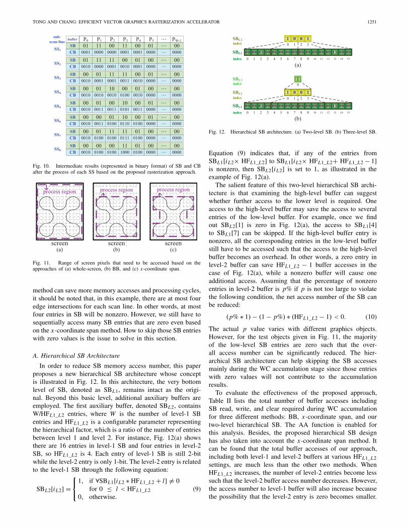
In summary, our proposed method will require two screen-wide buffers: one for SB and the other one for CB. The datawidth of a SB entry is 2, based on our proposed SB codingscheme. The data width of CB entry is 4 because at most eightsampling points are used for each pixel such that CV rangesfrom zero to eight. Fig. 10 shows the binary contents of bothbuffers after each SS has been processed for the objects givenin Fig. 4. After processing the last SS, the CV value of all thepixels in the current scan line will be produced.
V. NEW BUFFER ARCHITECTURE FOR
REDUCED MEMORY ACCESSES
In the previous section, we proposed two methods to reducethe size of SB required. In this section, we further presenta new SB architecture that can save many buffer memoryaccess operations. As mentioned before, to determine whethera pixel on the screen will be drawn or not depends on theWC of the corresponding pixel. The WC can be obtained fromaccumulating the FWC values stored in SB. It can be expectedthat many SB memory accesses will occur because we haveto fetch the WC from SB for every pixel on the screen, asillustrated in Fig. 11(a). However, most paths that constitutegraphics objects may occupy only partial screen. Therefore, wecan simply restrict the generation of WC to only those pixelsthat are located inside the rectangular bounding box (BB) ofthe path as illustrated in Fig. 11(b) such that the SB memoryaccesses for those pixels outside the box can be avoided. Tofurther reduce the SB operations, [12] proposes an even betterapproach called x-coordinate span which can determine therange of each scan line that requires WC generation. Sincedifferent scan lines may have different ranges, the minimumand maximum x-coordinate values of crossing points in thecurrent scan line have to be detected during FWC generation.Only those pixels between these two end points will be furtherprocessed. Fig. 11(c) illustrates the region of the pixels thatwill undergo the in–out test, which is smaller than the regionsshown in Fig. 11(b) based on the global BB. Although this
TONG AND CHANG: EFFICIENT VECTOR GRAPHICS RASTERIZATION ACCELERATOR 1251
Fig. 10. Intermediate results (represented in binary format) of SB and CBafter the process of each SS based on the proposed rasterization approach.
Fig. 11. Range of screen pixels that need to be accessed based on theapproaches of (a) whole-screen, (b) BB, and (c) x-coordinate span.
method can save more memory accesses and processing cycles,it should be noted that, in this example, there are at most fouredge intersections for each scan line. In other words, at mostfour entries in SB will be nonzero. However, we still have tosequentially access many SB entries that are zero even basedon the x-coordinate span method. How to skip those SB entrieswith zero values is the issue to solve in this section.
A. Hierarchical SB Architecture
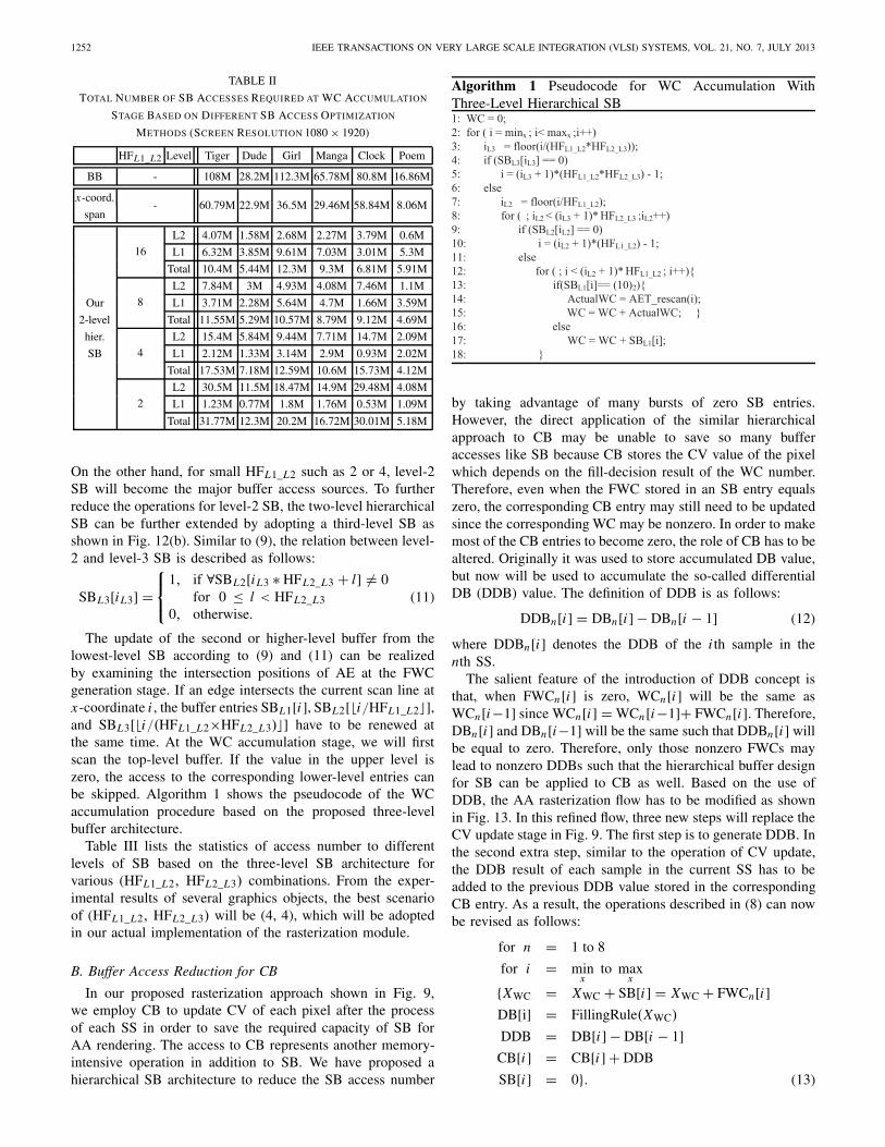
In order to reduce SB memory access number, this paperproposes a new hierarchical SB architecture whose conceptis illustrated in Fig. 12. In this architecture, the very bottomlevel of SB, denoted as SBL1, remains intact as the origi-nal. Beyond this basic level, additional auxiliary buffers areemployed. The first auxiliary buffer, denoted SBL2, containsW/HFL1_L2 entries, where W is the number of level-1 SBentries and HFL1_L2 is a configurable parameter representingthe hierarchical factor, which is a ratio of the number of entriesbetween level 1 and level 2. For instance, Fig. 12(a) showsthere are 16 entries in level-1 SB and four entries in level-2SB, so HFL1_L2 is 4. Each entry of level-1 SB is still 2-bitwhile the level-2 entry is only 1-bit. The level-2 entry is relatedto the level-1 SB through the following equation:
SBL2[iL2] =⎧⎨⎩
1, if ∀SBL1[iL2 ∗ HFL1_L2 + l] �= 0for 0 ≤ l < HFL1_L2
0, otherwise.(9)
Fig. 12. Hierarchical SB architecture. (a) Two-level SB. (b) Three-level SB.
Equation (9) indicates that, if any of the entries fromSBL1[iL2× HFL1_L2] to SBL1[iL2× HFL1_L2+ HFL1_L2 − 1]is nonzero, then SBL2[iL2] is set to 1, as illustrated in theexample of Fig. 12(a).
The salient feature of this two-level hierarchical SB archi-tecture is that examining the high-level buffer can suggestwhether further access to the lower level is required. Oneaccess to the high-level buffer may save the access to severalentries of the low-level buffer. For example, once we findout SBL2[1] is zero in Fig. 12(a), the access to SBL1[4]to SBL1[7] can be skipped. If the high-level buffer entry isnonzero, all the corresponding entries in the low-level bufferstill have to be accessed such that the access to the high-levelbuffer becomes an overhead. In other words, a zero entry inlevel-2 buffer can save HFL1_L2 − 1 buffer accesses in thecase of Fig. 12(a), while a nonzero buffer will cause oneadditional access. Assuming that the percentage of nonzeroentries in level-2 buffer is p% if p is not too large to violatethe following condition, the net access number of the SB canbe reduced:
(p% ∗ 1) − (1 − p%) ∗ (HFL1_L2 − 1) < 0. (10)
The actual p value varies with different graphics objects.However, for the test objects given in Fig. 11, the majorityof the low-level SB entries are zero such that the over-all access number can be significantly reduced. The hier-archical SB architecture can help skipping the SB accessesmainly during the WC accumulation stage since those entrieswith zero values will not contribute to the accumulationresults.
To evaluate the effectiveness of the proposed approach,Table II lists the total number of buffer accesses includingSB read, write, and clear required during WC accumulationfor three different methods: BB, x-coordinate span, and ourtwo-level hierarchical SB. The AA function is enabled forthis analysis. Besides, the proposed hierarchical SB designhas also taken into account the x-coordinate span method. Itcan be found that the total buffer accesses of our approach,including both level-1 and level-2 buffers at various HFL1_L2settings, are much less than the other two methods. WhenHFL1_L2 increases, the number of level-2 entries become lesssuch that the level-2 buffer access number decreases. However,the access number to level-1 buffer will also increase becausethe possibility that the level-2 entry is zero becomes smaller.
1252 IEEE TRANSACTIONS ON VERY LARGE SCALE INTEGRATION (VLSI) SYSTEMS, VOL. 21, NO. 7, JULY 2013
TABLE II
TOTAL NUMBER OF SB ACCESSES REQUIRED AT WC ACCUMULATION
STAGE BASED ON DIFFERENT SB ACCESS OPTIMIZATION
METHODS (SCREEN RESOLUTION 1080 × 1920)
HFL1_L2 Level Tiger Dude Girl Manga Clock Poem
BB - 108M 28.2M 112.3M 65.78M 80.8M 16.86M
x-coord.- 60.79M 22.9M 36.5M 29.46M 58.84M 8.06M
span
16
L2 4.07M 1.58M 2.68M 2.27M 3.79M 0.6M
L1 6.32M 3.85M 9.61M 7.03M 3.01M 5.3M
Total 10.4M 5.44M 12.3M 9.3M 6.81M 5.91M
8
L2 7.84M 3M 4.93M 4.08M 7.46M 1.1M
Our L1 3.71M 2.28M 5.64M 4.7M 1.66M 3.59M
2-level Total 11.55M 5.29M 10.57M 8.79M 9.12M 4.69M
hier.
4
L2 15.4M 5.84M 9.44M 7.71M 14.7M 2.09M
SB L1 2.12M 1.33M 3.14M 2.9M 0.93M 2.02M
Total 17.53M 7.18M 12.59M 10.6M 15.73M 4.12M
2
L2 30.5M 11.5M 18.47M 14.9M 29.48M 4.08M
L1 1.23M 0.77M 1.8M 1.76M 0.53M 1.09M
Total 31.77M 12.3M 20.2M 16.72M 30.01M 5.18M
On the other hand, for small HFL1_L2 such as 2 or 4, level-2SB will become the major buffer access sources. To furtherreduce the operations for level-2 SB, the two-level hierarchicalSB can be further extended by adopting a third-level SB asshown in Fig. 12(b). Similar to (9), the relation between level-2 and level-3 SB is described as follows:
SBL3[iL3] =⎧⎨⎩
1, if ∀SBL2[iL3 ∗ HFL2_L3 + l] �= 0for 0 ≤ l < HFL2_L3
0, otherwise.(11)
The update of the second or higher-level buffer from thelowest-level SB according to (9) and (11) can be realizedby examining the intersection positions of AE at the FWCgeneration stage. If an edge intersects the current scan line atx-coordinate i , the buffer entries SBL1[i ], SBL2[�i/HFL1_L2�],and SBL3[�i/(HFL1_L2×HFL2_L3)�] have to be renewed atthe same time. At the WC accumulation stage, we will firstscan the top-level buffer. If the value in the upper level iszero, the access to the corresponding lower-level entries canbe skipped. Algorithm 1 shows the pseudocode of the WCaccumulation procedure based on the proposed three-levelbuffer architecture.
Table III lists the statistics of access number to differentlevels of SB based on the three-level SB architecture forvarious (HFL1_L2, HFL2_L3) combinations. From the exper-imental results of several graphics objects, the best scenarioof (HFL1_L2, HFL2_L3) will be (4, 4), which will be adoptedin our actual implementation of the rasterization module.
B. Buffer Access Reduction for CB
In our proposed rasterization approach shown in Fig. 9,we employ CB to update CV of each pixel after the processof each SS in order to save the required capacity of SB forAA rendering. The access to CB represents another memory-intensive operation in addition to SB. We have proposed ahierarchical SB architecture to reduce the SB access number
Algorithm 1 Pseudocode for WC Accumulation WithThree-Level Hierarchical SB
by taking advantage of many bursts of zero SB entries.However, the direct application of the similar hierarchicalapproach to CB may be unable to save so many bufferaccesses like SB because CB stores the CV value of the pixelwhich depends on the fill-decision result of the WC number.Therefore, even when the FWC stored in an SB entry equalszero, the corresponding CB entry may still need to be updatedsince the corresponding WC may be nonzero. In order to makemost of the CB entries to become zero, the role of CB has to bealtered. Originally it was used to store accumulated DB value,but now will be used to accumulate the so-called differentialDB (DDB) value. The definition of DDB is as follows:
DDBn[i ] = DBn[i ] − DBn[i − 1] (12)
where DDBn[i ] denotes the DDB of the i th sample in thenth SS.
The salient feature of the introduction of DDB concept isthat, when FWCn [i ] is zero, WCn[i ] will be the same asWCn[i−1] since WCn[i ] = WCn [i−1]+ FWCn[i ]. Therefore,DBn[i ] and DBn[i−1] will be the same such that DDBn[i ] willbe equal to zero. Therefore, only those nonzero FWCs maylead to nonzero DDBs such that the hierarchical buffer designfor SB can be applied to CB as well. Based on the use ofDDB, the AA rasterization flow has to be modified as shownin Fig. 13. In this refined flow, three new steps will replace theCV update stage in Fig. 9. The first step is to generate DDB. Inthe second extra step, similar to the operation of CV update,the DDB result of each sample in the current SS has to beadded to the previous DDB value stored in the correspondingCB entry. As a result, the operations described in (8) can nowbe revised as follows:
for n = 1 to 8
for i = minx
to maxx
{XWC = XWC + SB[i ] = XWC + FWCn[i ]DB[i] = FillingRule(XWC)
DDB = DB[i ] − DB[i − 1]CB[i ] = CB[i ] + DDB
SB[i ] = 0}. (13)
TONG AND CHANG: EFFICIENT VECTOR GRAPHICS RASTERIZATION ACCELERATOR 1253
TABLE III
TOTAL NUMBER OF SB ACCESSES REQUIRED AT WC ACCUMULATION STAGE BASED
ON THREE-LEVEL SB ARCHITECTURE WITH VARIOUS PARAMETER SETTINGS
Tiger Dude Girl Manga Clock Poem
LevelHFL2_L3 HFL2_L3 HFL2_L3 HFL2_L3 HFL2_L3 HFL2_L3
HFL1_L2 4 8 4 8 4 8 4 8 4 8 4 8
2
L3 7.84M 4.07M 3M 1.58M 4.93M 2.68M 4.08M 2.27M 7.46M 3.79M 1.1M 0.6ML2 1.99M 3.3M 1.22M 2.01M 3.02M 5.01M 2.57M 3.74M 0.89M 1.56M 1.84M 2.7ML1 1.23M 1.23M 0.77M 0.77M 1.8M 1.8M 1.76M 1.76M 0.53M 0.53M 1.09M 1.09M
Total 11.07M 8.61M 5M 4.37M 9.76M 9.5M 8.43M 7.78M 8.88M 5.89M 4.04M 4.4M
4
L3 4.07M 2.18M 1.58M 0.87M 2.68M 1.55M 2.27M 1.36 3.79M 1.96M 0.6M 0.35ML2 1.79M 2.79M 1.08M 1.65M 2.71M 4.13M 2.1M 2.68M 0.84M 1.47M 1.4M 1.79ML1 2.12M 2.12M 1.33M 1.33M 3.14M 3.14M 2.9M 2.9M 0.93M 0.93M 2.02M 2.02M
Total 7.99M 7.1M 4.01M 3.86M 8.54M 8.82M 7.28M 6.96M 5.57M 4.37M 4.04M 4.18M
8
L3 2.18M 1.23M 0.87M 0.51M 1.55M 0.98M 1.36M 0.91M 1.96M 1.03M 0.35M 0.23ML2 1.53M 2.26M 0.91M 1.37M 2.27M 3.15M 1.57M 1.87M 0.79M 1.3M 0.95M 1.05ML1 3.71M 3.71M 2.28M 2.28M 5.64M 5.64M 4.7M 4.7M 1.66M 1.66M 3.59M 3.59M
Total 7.43M 7.2M 4.07M 4.16M 9.47M 9.78M 7.64M 7.49M 4.42M 4M 4.9M 4.87M
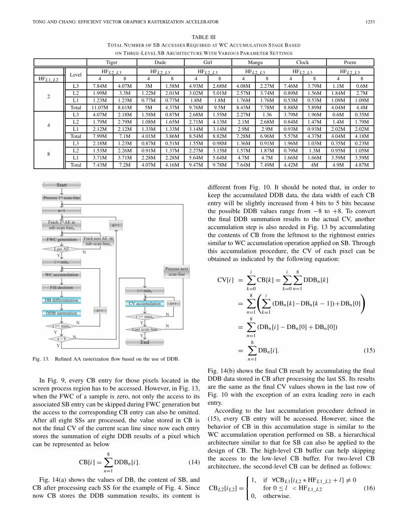
Fig. 13. Refined AA rasterization flow based on the use of DDB.
In Fig. 9, every CB entry for those pixels located in thescreen process region has to be accessed. However, in Fig. 13,when the FWC of a sample is zero, not only the access to itsassociated SB entry can be skipped during FWC generation butthe access to the corresponding CB entry can also be omitted.After all eight SSs are processed, the value stored in CB isnot the final CV of the current scan line since now each entrystores the summation of eight DDB results of a pixel whichcan be represented as below
CB[i ] =8∑
n=1
DDBn[i ]. (14)
Fig. 14(a) shows the values of DB, the content of SB, andCB after processing each SS for the example of Fig. 4. Sincenow CB stores the DDB summation results, its content is
different from Fig. 10. It should be noted that, in order tokeep the accumulated DDB data, the data width of each CBentry will be slightly increased from 4 bits to 5 bits becausethe possible DDB values range from −8 to +8. To convertthe final DDB summation results to the actual CV, anotheraccumulation step is also needed in Fig. 13 by accumulatingthe contents of CB from the leftmost to the rightmost entriessimilar to WC accumulation operation applied on SB. Throughthis accumulation procedure, the CV of each pixel can beobtained as indicated by the following equation:
CV[i ] =i∑
k=0
CB[k] =i∑
k=0
8∑n=1
DDBn[k]
=8∑
n=1
(i∑
k=1
(DBn[k]−DBn[k − 1])+DBn[0])
=8∑
n=1
(DBn[i ] − DBn[0] + DBn[0])
=8∑
n=1
DBn[i ]. (15)
Fig. 14(b) shows the final CB result by accumulating the finalDDB data stored in CB after processing the last SS. Its resultsare the same as the final CV values shown in the last row ofFig. 10 with the exception of an extra leading zero in eachentry.
According to the last accumulation procedure defined in(15), every CB entry will be accessed. However, since thebehavior of CB in this accumulation stage is similar to theWC accumulation operation performed on SB, a hierarchicalarchitecture similar to that for SB can also be applied to thedesign of CB. The high-level CB buffer can help skippingthe access to the low-level CB buffer. For two-level CBarchitecture, the second-level CB can be defined as follows:
CBL2[iL2] =⎧⎨⎩
1, if ∀CBL1[iL2 ∗ HFL1_L2 + l] �= 0for 0 ≤ l < HFL1_L2
0, otherwise.(16)
1254 IEEE TRANSACTIONS ON VERY LARGE SCALE INTEGRATION (VLSI) SYSTEMS, VOL. 21, NO. 7, JULY 2013
(a)
(b)
Fig. 14. Buffer content based on the new AA rasterization shown in Fig. 13 for (a) SB and CB after the process of each SS and (b) CB after final CVaccumulation procedure.
TABLE IV
COMPARISON OF CB ACCESS NUMBER FOR DIFFERENT CB DESIGNS
DB architecture Level Tiger Dude Girl Manga Clock Poem
No 1-Level CV- 60.83M 22.9M 36.5M 29.5M 58.8M 8.07M
DDB CB update
DDBL1 0.74M 0.43M 1.09M 1.08M 0.32M 0.53M
With 1-Level summ.DDB CB CV acc. L1 7.7M 2.92M 4.67M 3.78M 7.39M 1.03M
Total - 8.44M 3.36M 5.77M 4.87M 7.71M 1.57M
DDB L2 0.37M 0.21M 0.54M 0.54M 0.16M 0.26MWith 2-Level summ. L1 0.74M 0.43M 1.09M 1.08M 0.32M 0.53MDDB CB
CV acc.L2 2.0M 0.77M 1.28M 1.06M 1.88M 0.31ML1 0.42M 0.23M 0.55M 0.5M 0.17M 0.3M
Total - 3.54M 1.66M 3.48M 3.19M 2.53M 1.41M
Table IV compares the number of buffer accesses of CB fordifferent DB designs including the ordinary DB design withoutDDB mechanism, one-level CB with DDB mechanism, andtwo-level CB with DDB mechanism. The parameter HFL1_L2is set to 4. As expected, the memory access number can bereduced by at least a factor of five for those test objectsshown in Fig. 8. Since the number of level-2 CB accessesis not very large, an additional level-3 CB will not be furtherconsidered.
VI. CIRCUIT DESIGN OF RASTERIZATION MODULE
In this section, the actual circuit design issues of therasterization accelerator module are addressed. In additionto presenting our design based on the proposed bufferoptimization techniques, to make a fair comparison, thedesign of the conventional rasterization processing flowshown in Fig. 3 is also presented. Both designs will sup-port the AA function based on the 8-queen multisamplingpattern.
Fig. 15. Circuit diagram of the conventional rasterization accelerator.
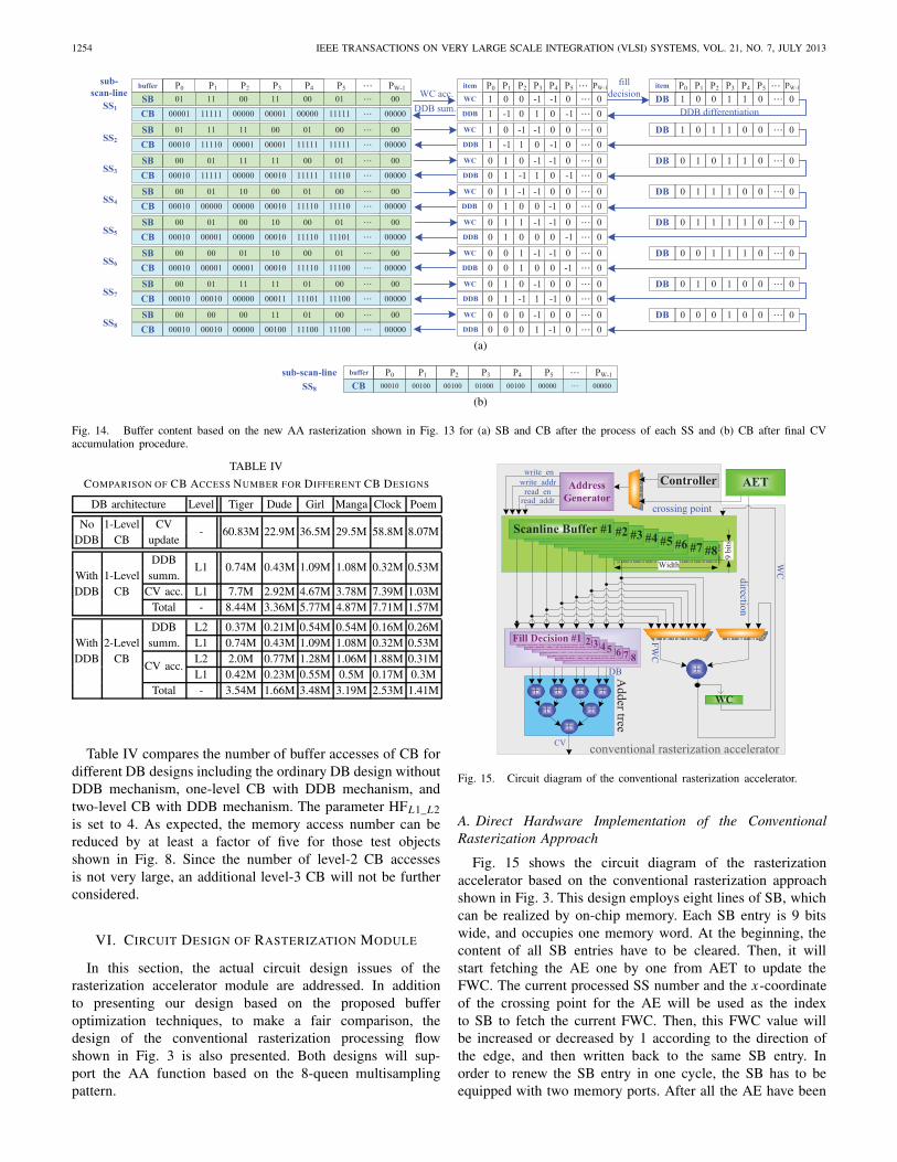
A. Direct Hardware Implementation of the ConventionalRasterization Approach
Fig. 15 shows the circuit diagram of the rasterizationaccelerator based on the conventional rasterization approachshown in Fig. 3. This design employs eight lines of SB, whichcan be realized by on-chip memory. Each SB entry is 9 bitswide, and occupies one memory word. At the beginning, thecontent of all SB entries have to be cleared. Then, it willstart fetching the AE one by one from AET to update theFWC. The current processed SS number and the x-coordinateof the crossing point for the AE will be used as the indexto SB to fetch the current FWC. Then, this FWC value willbe increased or decreased by 1 according to the direction ofthe edge, and then written back to the same SB entry. Inorder to renew the SB entry in one cycle, the SB has to beequipped with two memory ports. After all the AE have been
TONG AND CHANG: EFFICIENT VECTOR GRAPHICS RASTERIZATION ACCELERATOR 1255
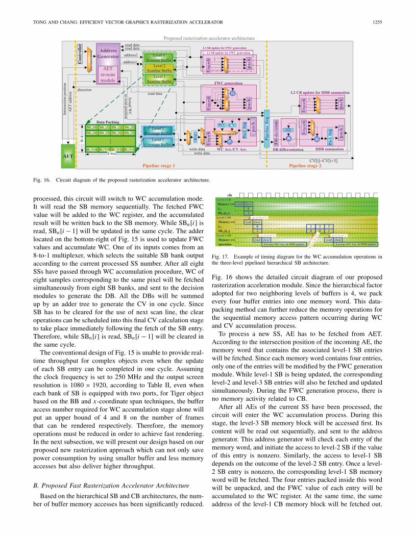
Fig. 16. Circuit diagram of the proposed rasterization accelerator architecture.
processed, this circuit will switch to WC accumulation mode.It will read the SB memory sequentially. The fetched FWCvalue will be added to the WC register, and the accumulatedresult will be written back to the SB memory. While SBn[i ] isread, SBn[i − 1] will be updated in the same cycle. The adderlocated on the bottom-right of Fig. 15 is used to update FWCvalues and accumulate WC. One of its inputs comes from an8-to-1 multiplexer, which selects the suitable SB bank outputaccording to the current processed SS number. After all eightSSs have passed through WC accumulation procedure, WC ofeight samples corresponding to the same pixel will be fetchedsimultaneously from eight SB banks, and sent to the decisionmodules to generate the DB. All the DBs will be summedup by an adder tree to generate the CV in one cycle. SinceSB has to be cleared for the use of next scan line, the clearoperations can be scheduled into this final CV calculation stageto take place immediately following the fetch of the SB entry.Therefore, while SBn[i ] is read, SBn[i − 1] will be cleared inthe same cycle.
The conventional design of Fig. 15 is unable to provide real-time throughput for complex objects even when the updateof each SB entry can be completed in one cycle. Assumingthe clock frequency is set to 250 MHz and the output screenresolution is 1080 × 1920, according to Table II, even wheneach bank of SB is equipped with two ports, for Tiger objectbased on the BB and x-coordinate span techniques, the bufferaccess number required for WC accumulation stage alone willput an upper bound of 4 and 8 on the number of framesthat can be rendered respectively. Therefore, the memoryoperations must be reduced in order to achieve fast rendering.In the next subsection, we will present our design based on ourproposed new rasterization approach which can not only savepower consumption by using smaller buffer and less memoryaccesses but also deliver higher throughput.
B. Proposed Fast Rasterization Accelerator Architecture
Based on the hierarchical SB and CB architectures, the num-ber of buffer memory accesses has been significantly reduced.
Fig. 17. Example of timing diagram for the WC accumulation operations inthe three-level pipelined hierarchical SB architecture.
Fig. 16 shows the detailed circuit diagram of our proposedrasterization acceleration module. Since the hierarchical factoradopted for two neighboring levels of buffers is 4, we packevery four buffer entries into one memory word. This data-packing method can further reduce the memory operations forthe sequential memory access pattern occurring during WCand CV accumulation process.
To process a new SS, AE has to be fetched from AET.According to the intersection position of the incoming AE, thememory word that contains the associated level-1 SB entrieswill be fetched. Since each memory word contains four entries,only one of the entries will be modified by the FWC generationmodule. While level-1 SB is being updated, the correspondinglevel-2 and level-3 SB entries will also be fetched and updatedsimultaneously. During the FWC generation process, there isno memory activity related to CB.
After all AEs of the current SS have been processed, thecircuit will enter the WC accumulation process. During thisstage, the level-3 SB memory block will be accessed first. Itscontent will be read out sequentially, and sent to the addressgenerator. This address generator will check each entry of thememory word, and initiate the access to level-2 SB if the valueof this entry is nonzero. Similarly, the access to level-1 SBdepends on the outcome of the level-2 SB entry. Once a level-2 SB entry is nonzero, the corresponding level-1 SB memoryword will be fetched. The four entries packed inside this wordwill be unpacked, and the FWC value of each entry will beaccumulated to the WC register. At the same time, the sameaddress of the level-1 CB memory block will be fetched out.
1256 IEEE TRANSACTIONS ON VERY LARGE SCALE INTEGRATION (VLSI) SYSTEMS, VOL. 21, NO. 7, JULY 2013
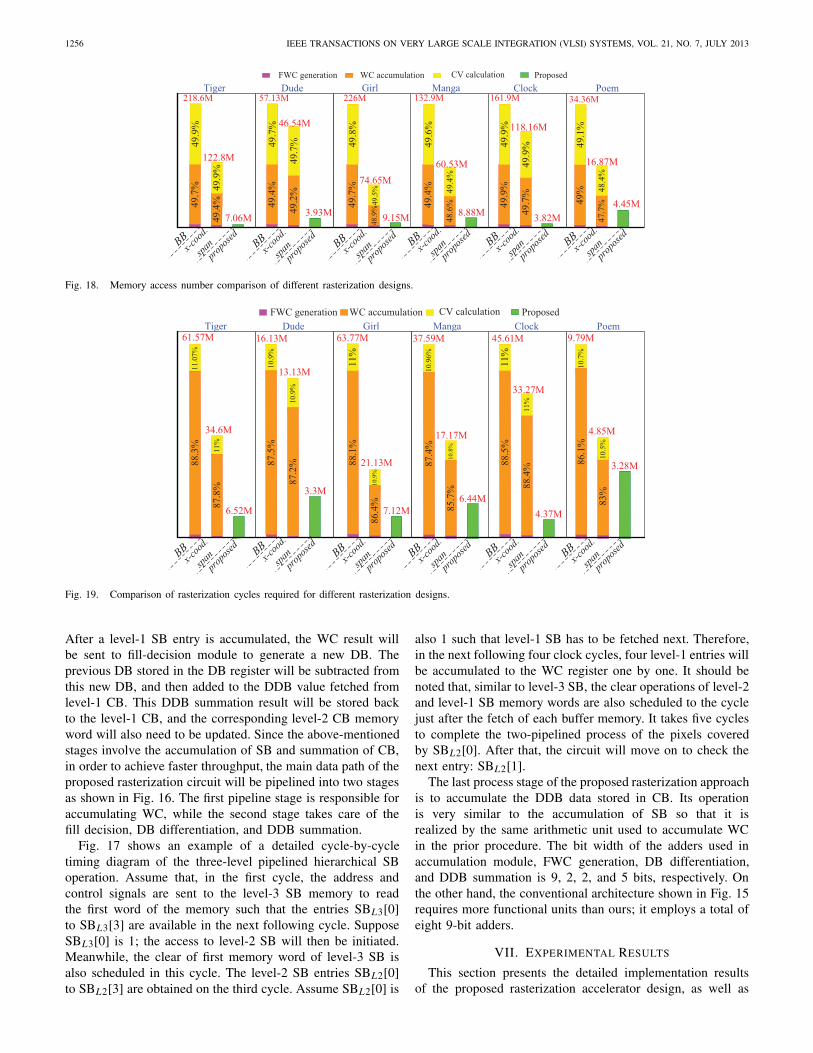
Fig. 18. Memory access number comparison of different rasterization designs.
Fig. 19. Comparison of rasterization cycles required for different rasterization designs.
After a level-1 SB entry is accumulated, the WC result willbe sent to fill-decision module to generate a new DB. Theprevious DB stored in the DB register will be subtracted fromthis new DB, and then added to the DDB value fetched fromlevel-1 CB. This DDB summation result will be stored backto the level-1 CB, and the corresponding level-2 CB memoryword will also need to be updated. Since the above-mentionedstages involve the accumulation of SB and summation of CB,in order to achieve faster throughput, the main data path of theproposed rasterization circuit will be pipelined into two stagesas shown in Fig. 16. The first pipeline stage is responsible foraccumulating WC, while the second stage takes care of thefill decision, DB differentiation, and DDB summation.
Fig. 17 shows an example of a detailed cycle-by-cycletiming diagram of the three-level pipelined hierarchical SBoperation. Assume that, in the first cycle, the address andcontrol signals are sent to the level-3 SB memory to readthe first word of the memory such that the entries SBL3[0]to SBL3[3] are available in the next following cycle. SupposeSBL3[0] is 1; the access to level-2 SB will then be initiated.Meanwhile, the clear of first memory word of level-3 SB isalso scheduled in this cycle. The level-2 SB entries SBL2[0]to SBL2[3] are obtained on the third cycle. Assume SBL2[0] is
also 1 such that level-1 SB has to be fetched next. Therefore,in the next following four clock cycles, four level-1 entries willbe accumulated to the WC register one by one. It should benoted that, similar to level-3 SB, the clear operations of level-2and level-1 SB memory words are also scheduled to the cyclejust after the fetch of each buffer memory. It takes five cyclesto complete the two-pipelined process of the pixels coveredby SBL2[0]. After that, the circuit will move on to check thenext entry: SBL2[1].
The last process stage of the proposed rasterization approachis to accumulate the DDB data stored in CB. Its operationis very similar to the accumulation of SB so that it isrealized by the same arithmetic unit used to accumulate WCin the prior procedure. The bit width of the adders used inaccumulation module, FWC generation, DB differentiation,and DDB summation is 9, 2, 2, and 5 bits, respectively. Onthe other hand, the conventional architecture shown in Fig. 15requires more functional units than ours; it employs a total ofeight 9-bit adders.
VII. EXPERIMENTAL RESULTS
This section presents the detailed implementation resultsof the proposed rasterization accelerator design, as well as
TONG AND CHANG: EFFICIENT VECTOR GRAPHICS RASTERIZATION ACCELERATOR 1257
TABLE V
PROFILE OF MEMORY ACCESS TIMES AND NUMBER OF CYCLES FOR PROPOSED RASTERIZATION SCHEME
Processing stages r/wMemory access times No. of cycles
Tiger Dude Girl Manga Clock Poem Tiger Dude Girl Manga Clock PoemL3 SB Write 0.38M 0.23M 0.55M 0.57M 0.16M 0.3M
0.38M 0.23M 0.55M 0.57M 0.16M 0.3M
L3 SB Read 0.38M 0.23M 0.55M 0.57M 0.16M 0.3MFWC L2 SB Write 0.38M 0.23M 0.55M 0.57M 0.16M 0.3M
generation L2 SB Read 0.38M 0.23M 0.55M 0.57M 0.16M 0.3ML1 SB Write 0.38M 0.23M 0.55M 0.57M 0.16M 0.3ML1 SB Read 0.38M 0.23M 0.55M 0.57M 0.16M 0.3M
AET rescan Read 1.08K 1.2K 0.06K 2.6K 0.83K 89.2K 1.08K 1.2K 0.06K 2.6K 0.83K 89.2KL3 SB Read 0.61M 0.25M 0.49M 0.45M 0.51M 0.11M
2.03M 0.79M 1.34M 1.13M 1.89M 0.3MWC L3 SB Clear 0.61M 0.25M 0.49M 0.45M 0.51M 0.11M
accumulation L2 SB Read 0.32M 0.19M 0.5M 0.43M 0.15M 0.21M0.89M 0.54M 1.35M 1.05M 0.42M 0.7M
L2 SB Clear 0.32M 0.19M 0.5M 0.43M 0.15M 0.21ML1 SB Read 0.36M 0.22M 0.54M 0.53M 0.16M 0.29M
1.83M 1.13M 2.72M 2.56M 0.8M 1.46M
L1 SB Clear 0.36M 0.22M 0.54M 0.53M 0.16M 0.29ML2 CB Write 0.36M 0.21M 0.54M 0.51M 0.15M 0.26M
DDB L2 CB Read 0.36M 0.21M 0.54M 0.51M 0.15M 0.26Msummation L1 CB Write 0.36M 0.21M 0.54M 0.51M 0.15M 0.26M
L1 CB Read 0.36M 0.21M 0.54M 0.51M 0.15M 0.26ML2 CB Read 0.25M 0.1M 0.17M 0.14M 0.23M 0.03M
1M 0.38M 0.64M 0.53M 0.94M 0.15MCV L2 CB Clear 0.25M 0.1M 0.17M 0.14M 0.23M 0.03M
accumulation L1 CB Read 0.09M 0.05M 0.12M 0.12M 0.03M 0.06M0.36M 0.2M 0.5M 0.48M 0.15M 0.25M
L1 CB Clear 0.09M 0.05M 0.12M 0.12M 0.03M 0.06MTotal – 7.06M 3.93M 9.15M 8.88M 3.82M 4.45M 6.52M 3.3M 7.12M 6.44M 4.37M 3.28M
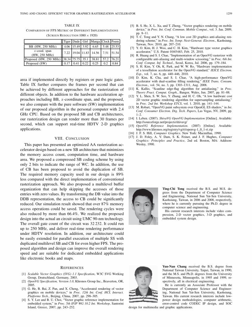
its comparisons with other approaches. Figs. 18 and 19 firstcompare the number of memory accesses and execution cyclesrequired by our proposed, BB, and x-coordinate span designs.The detailed profiling of the performance figures for the lattertwo approaches is also included. The profiling of our proposeddesign cannot be clearly presented in the same bar charts, soonly the total memory access number and cycles are given. Thedetailed statistics of memory access number and cycles of theproposed method at different stages for various levels of SBand CB are listed in Table V. The graphics objects used in ourexperiment are rendered with the AA function enabled underthe screen resolution of 1080×1920. Both hierarchical SB andCB techniques are implemented in our rasterization module.Fig. 18 reveals that WC accumulation and CV calculationare two major operations which together consume more than90% of the memory accesses in the conventional rasterizationapproach. Although the proposed hierarchical buffer designwill not help reduce the memory accesses during FWC gener-ation, it indeed can significantly reduce the required memoryoperations for the two most memory-consuming processingstages. The actual reduction ratios vary with different objects.For those objects that contain large but simple paths such asthe outline of Tiger’s head, Girl’s figure, Manga’s figure, andClock’s frame, the reduction ratio will be higher because thedistances of the neighboring intersection points in these pathsare larger. On the other hand, in the example of Poem, it isbuilt mostly by the small but complex paths like the font’soutline, so the saving is comparatively small. On average, ourapproach can save about 87%–97.6% and 73.6%–96.7% ofmemory accesses, respectively, compared with the other twoapproaches.
According to Fig. 18, WC accumulation and CV calculationin the conventional rasterization approach demand almost the
same amount of memory accesses. However, we assume that,during CV calculation, all the SS buffers are accessed inparallel such that the cycles spent in this stage are much lessthan those in the WC accumulation stage. However, there arestill large numbers of cycles wasted to access those zero bufferentries. Fig. 19 shows that the average saving of 66.4%–90.4%and 32.3%–86.8% can be achieved by our design comparedwith the BB and x-coordinate span approaches, respectively.
Table V provides further analysis of memory accesses andexecution cycles required in the proposed rasterization module.In the FWC generation stage, all the three levels of SBmemory blocks will be fetched and updated concurrently. Thenumber of cycles spent in this stage depends on the numberof intersection points of objects and scan lines. In the WCaccumulation stage, the access to the low-level buffers dependson the content of the upper-level buffers such that three levelsof buffers will not be accessed in parallel. Table V lists thecycles spent in the access to each SB buffer. For CB buffer,during DDB summation, all levels of CB are accessed inparallel with the access to level-1 SB buffer. In the finalCV accumulation stage, similar to the behavior of SB inWC accumulation stage, the access to low-level CB bufferdepends on the content of the higher level buffer. The AETrescan cycles for over-bound WC values are also taken intoconsideration in Table V, and, as expected, this overhead issmall and can almost be neglected. In contrast to BB and x-coordinate span, there is no obvious dominant stage in ourproposed rasterization flow.
It has been shown that, if for some scan lines the percentage(p%) of nonzero entries in the upper-level buffer does notsatisfy (10), the proposed hierarchical buffer design will causemore memory accesses. Since HFL1_L2 is 4 in our design, andconsidering only the relationship between level-1 and level-2
1258 IEEE TRANSACTIONS ON VERY LARGE SCALE INTEGRATION (VLSI) SYSTEMS, VOL. 21, NO. 7, JULY 2013
TABLE VI
COMPLEXITY AND PROFILING ANALYSIS OF THE TEST OBJECTS
(SCREEN RESOLUTION 1080 × 1920)
Tiger Dude Girl Manga Clock Poem
No. of paths 305 167 92 242 85 42
No. of processed19 270 10 900 27 694 29 190 7848 6802
scan lines
No. of processed SS 152 516 86 024 220 840 231 816 62 195 54 369
No. of DS 21 996 15 109 13 026 67 578 7526 1254
No. of non-DS 130 520 70 915 207 814 164 238 54 669 53 115
Span length of DS 4.55 5.00 5.19 4.45 5.56 6.05
Span length of232.12 160.4 87.58 87.87 537.4 75.82
non-DS
No. of filled pixels 3.59M 1.31M 1.61M 1.74M 2.23M 0.27M
No. of max.18 54 14 14 6 16
crossings/SS
TABLE VII
COMPARISON OF BUFFER SIZE AND ERROR RATIO FOR
DIFFERENT RASTERIZATION APPROACHES
Terms Objects240 × 480 × 1080 ×
320 640 1920
Non-AA
Conventional Buffer size – 2160 4320 9720
Proposed Buffer
SBL3 – 15 30 68SBL2 – 60 120 270SBL1 – 480 960 2160Total – 555 1110 2498
AA
ConventionalBuffer size – 17 280 34 560 77 760Error ratio – 0% 0% 0%
[12]
Buffer size – 2880 5760 12960
Error ratio
Tiger 0.1079% 0.0582% 0.0843%Dude 0% 0% 0.0014%Girl 0% 0.0009% 0.0002%
Manga 0.13% 0.104% 0.0886%Clock 0.0098% 0.0031% 0.0016%Poem 1.082% 0.2618% 0.0933%
Proposed
SBL3 – 15 30 68SBL2 – 60 120 270
Buffer SBL1 – 480 960 2160size CBL2 – 60 120 270
CBL1 – 1200 2400 5400Total – 1815 3630 8168
Error ratio – 0% 0% 0%
buffers, p in (10) in level-2 buffer has to be less than 75.To find out the occurring chance of these densely intersectedscan lines (DS) whose p value is greater than 75, Table VIprovides some profiling analysis of the six graphics objectsfor the target screen resolution of 1080×1920. Here, the ratioof DS in the overall scan lines can be only 2.3% for Poemor up to more than 14.4% for Tiger. Although most of scanlines in Poem are non-DS, the average span length, definedas the distance in pixels between the first and last intersectionpoints, is only about one-third of the span length of Tiger suchthat Poem’s memory saving ratio is not as good as those ofthe others. In all six examples, the average span length of DSis only around 4–6 because these DSs are caused by thosepaths used to describe tiny objects such as Tiger’s whiskers.Therefore, the side effect of DS can be neglected although it
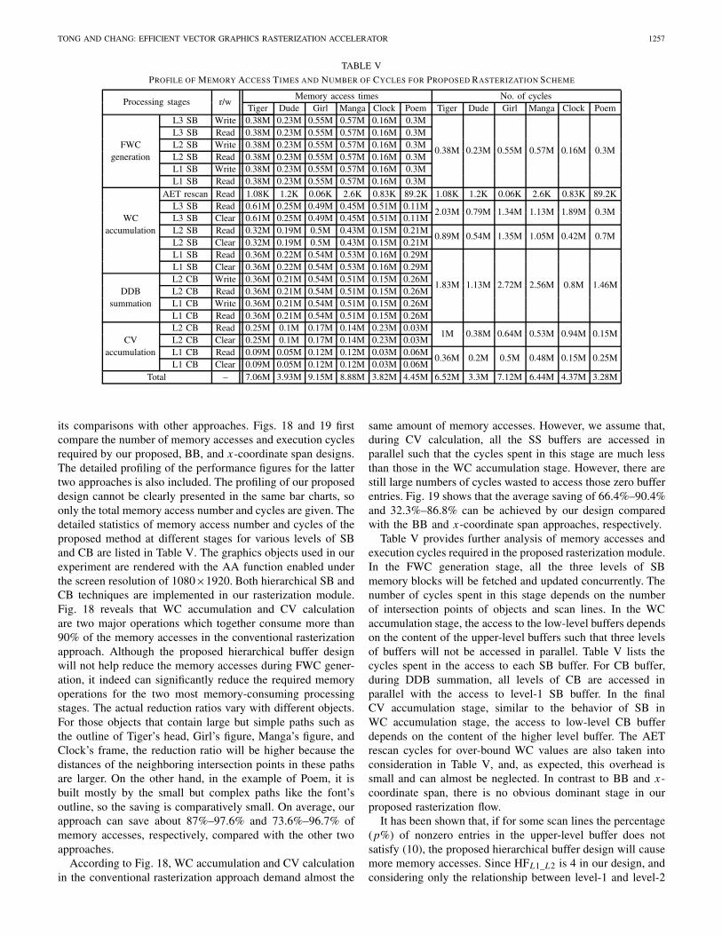
Fig. 20. Comparison of the distorted and normal rendering results of objects(a) Tiger. (b) Manga.
TABLE VIII
GATE-COUNT INFORMATION OF OUR PROPOSED RASTERIZATION
ACCELERATOR CIRCUIT (SCREEN RESOLUTION 1080 × 1920)
Modules Memory architecture Memory capacity (bits) Gate count
L3 SB Two-port 68 3360L2 SB Two-port 270 4219L1 SB Two-port 2160 9332L2 CB Single-port 270 3298L1 CB Single-port 5400 8946others N/A N/A 3077
total N/A 8168 32 232
can be completely avoided by using an additional counter tocount the number of nonzero entries in level-2 SB during theFWC generation stage. Once a threshold, which correspondsto 75% nonzero ratio, has been reached by the counter, theaccess to the high-level buffer can be disabled for the currentSS to avoid the side effect.
Finally, Table VII compares the total buffer size requiredfor various rasterization accelerator designs based on SBrendering. It can be found that the method of [12] can save83% buffer capacity compared with the conventional approach;however, its rendering image may be distorted. The renderingresults in [12] have been compared with the images renderedby the conventional approach. The error ratio calculated bydividing the number of different pixels with the total number ofrendering pixels is also listed in Table VII. Although the errorratio of [12] seems small, it cannot be neglected in the aspectof visual quality for particular test images. Fig. 20 shows twodistorted image examples. The regions near Tiger mouth ofFig. 20(a) and the waist of Girl of Fig. 20(b) appear wrongand cannot be ignored. On the contrary, our approach cannot only preserve the quality but also reduce buffer size. Thetotal buffer size required in our proposed scheme includingthree levels of SB and two levels of CB equals (W/(HFL1_L2×HFL2_L3))+ (W/HFL1_L2) + W × 2+ (W/HFL1_L2) + W × 5bits. By substituting the real number into this formula, the sizecan be calculated as given in Table VII. The saving of buffersize is approximately 89%.
We have realized the hardware implementation of the pro-posed architecture shown in Fig. 16, and synthesized thecircuit using UMC 90-nm technology under 250 MHz workingfrequency. As shown in Table VIII, the overall design costs32 232 gates. The gate count includes the area of all buffermemory blocks but excludes the area of AET. Up to morethan 90% of the overall rasterization circuit is occupied bymemory modules. The gate-count information of buffers listedin Table VIII is obtained according to the synthesized results,although for smaller memory blocks they may consume less
TONG AND CHANG: EFFICIENT VECTOR GRAPHICS RASTERIZATION ACCELERATOR 1259
TABLE IX
COMPARISON OF FPS METRIC OF DIFFERENT IMPLEMENTATIONS
(SCREEN RESOLUTION 1080 × 1920)
Tiger Dude Girl Manga Clock Poem
BB (HW, 250 MHz) 4.06 15.49 3.92 6.65 5.48 25.53x-cood. span
7.22 19.04 11.83 14.56 7.51 51.54(HW, 250 MHz)
Proposed (HW, 250 MHz) 38.34 75.75 35.1 38.81 57.2 76.21Proposed (SW) 0.17 0.41 0.22 0.25 0.2 0.84
area if implemented directly by registers or pure logic gates.Table IX further compares the frames per second that canbe achieved by different approaches for the rasterization ofdifferent objects. In addition to the hardware acceleration ap-proaches including BB, x-coordinate span, and the proposed,we also compare with the pure software (SW) implementationof our proposed algorithm in the personal computer with 2.4GHz CPU. Based on the proposed SB and CB architectures,our rasterization design can render more than 30 frames persecond, which can support real-time HDTV 2-D graphicsapplications.
VIII. CONCLUSION
This paper has presented an optimized AA rasterization ac-celerator design based on a new SB architecture that minimizesthe memory access count, computation time, and hardwarearea. We proposed a compressed SB coding scheme by usingonly 2 bits to indicate the range of WC. In addition, the useof CB has been proposed to avoid the duplication of SB.The required memory capacity used in our design is 89%less compared with the direct implementation of conventionalrasterization approach. We also proposed a multilevel bufferorganization that can help skipping the accesses of thoseentries with zero values. By transforming the DB value into theDDB representation, the access to CB could be significantlyreduced. Our simulation result showed that over 87% memoryaccess operations could be saved. The rendering cycles werealso reduced by more than 66.4%. We realized the proposeddesign into the actual an circuit using UMC 90-nm technology.The overall gate count of the circuit was 32 232. It could runup to 250 MHz, and deliver real-time rendering performanceunder HDTV resolution. In addition, our architecture couldbe easily extended for parallel execution of multiple SS withduplicated multilevel SB and CB for even higher FPS. The pro-posed algorithm and design can improve the overall renderingspeed and are suitable for dedicated embedded applicationslike electronic books and maps.
REFERENCES
[1] Scalable Vector Graphics (SVG) 1.1 Specification, W3C SVG WorkingGroup, Deutschland, Germany, 2003.
[2] OpenVG Specification, Version 1.0, Khronos Group Inc., Beaverton, OR,2005.
[3] G. He, B. Bai, Z. Pan, and X. Cheng, “Accelerated rendering of vectorgraphics on mobile devices,” in Proc. 12th Int. Conf. HCI, Interact.Platforms Tech., Beijing, China, 2007, pp. 298–305.
[4] S. Y. Lee and B. U. Choi, “Vector graphic reference implementation forembedded system,” in Proc. 5th IFIP WG 10.2 Int. Workshop, SantoriniIsland, Greece, 2007, pp. 243–252.
[5] B. S. He, X. L. Xu, and T. Zheng, “Vector graphics rendering on mobiledevice,” in Proc. Int. Conf. Commun. Mobile Comput., vol. 3. Jan. 2009,pp. 8–11.
[6] T. C. Tong and Y. N. Chang, “A low cost 2D graphics anti-aliasing ren-dering scheme,” in Proc. Int. Symp. Next-Generat. Electron., Kaohsiung,Taiwan, Nov. 2010, pp. 207–210.
[7] Y. O. Kim, H. J. Woo, and C. H. Kim, “Hardware type vector graphicsaccelerator,” U.S. Patent 0 045 683, Feb. 25, 2010.
[8] R. Huang and S. I. Chae, “Implementation of an OpenVG rasterizer withconfigurable anti-aliasing and multi-window scissoring,” in Proc. 6th Int.Conf. Comput. Inf. Technol., Seoul, Korea, Jul. 2006, pp. 179–184.
[9] S. H. Kim, Y. Oh, K. Park, and W. W. Ro, “Hardware implementationof a tessellation accelerator for the OpenVG standard,” IEICE Electron.Exp., vol. 7, no. 6, pp. 440–446, 2010.
[10] D. Kim, K. Cha, and S. I. Chae, “A high-performance OpenVGaccelerator with dual-scanline filling rendering,” IEEE Trans. Consum.Electron., vol. 54, no. 3, pp. 1303–1311, Aug. 2008.
[11] K. Kallio, “Scanline edge-flag algorithm for antialiasing,” in Proc.Theory Pract. Comput. Graph., Bangor, Wales, Jun. 2007, pp. 81–88.
[12] Y. L. Shen, S. W. Seo, Y. Zhang, and H. C. Oh, “A low hardware cost2D vector graphic rendering algorithm for supersampling antialiasing,”in Proc. 2nd Int. Workshop ETCS, vol. 1. 2010, pp. 141–144.
[13] M. Robart, “OpenVG paint subsystem over OpenGL ES shaders,” in Int.Conf. Consumer Electron. Dig. Tech. Papers, Las Vegas, NV, 2009, pp.1–2.
[14] I. Leben. (2007). ShivaVG OpenVG Implementation [Online]. Available:http://sourceforge.net/projects/shivavg/
[15] OpenVG Reference Implementation. (2007) [Online]. Available:http://www.khronos.org/registry/vg/ri/openvg-1_0_1-ri.zip
[16] J. F. S. Hill, Computer Graphics. New York: Macmillan, 1990.[17] J. D. Foley, A. V. Dam, S. K. Feiner, and J. F. Hughes, Computer
Graphics: Principles and Practice, 2nd ed. Boston, MA: Addison-Wesley, 1990.
Ting-Chi Tong received the B.S. and M.S. de-grees from the Department of Computer Scienceand Engineering, National Sun Yat-Sen University,Kaohsiung, Taiwan, in 2006 and 2008, respectively,where he is currently pursuing the Ph.D. degree incomputer science and engineering.
His current research interests include video com-pression, 2-D vector graphics, 3-D graphics, andembedded system design.
Yun-Nan Chang received the B.S. degree fromNational Taiwan University, Taipei, Taiwan, in 1990,and the M.S. and Ph.D. degrees from the Universityof Minnesota, Minneapolis, in 1995 and 1999, re-spectively, all in electrical engineering.
He is currently an Associate Professor with theDepartment of Computer Science and Engineer-ing, National Sun Yat-Sen University, Kaohsiung,Taiwan. His current research interests include low-power design methodologies, computer arithmetic,error-control code CODEC IP design, and SOC
design for multimedia and graphic applications.
Recommended