Satyam Kapil
EFFECTIVE DESIGN OF STATCOM CON-SIDERING FUNDAMENTAL FREQUENCY CURRENT, ACTIVE HARMONIC FILTER-ING AND ZERO SEQUENCE CURRENT
Faculty of Information Technology and Communication Science
Master of Science Thesis November 2019

i
ABSTRACT
SATYAM KAPIL: Effective Design of STATCOM Considering Fundamental Frequency
Current, Active Harmonic Filtering and Zero Sequence Current
Master of Science Thesis, 90 pages
Tampere University
Master’s Degree Programme in Electrical Engineering
November 2019
The main objective of this thesis was to investigate the effect of parallel reactive power com-pensation (RPC) and active harmonic filtering (AHF) operation on a STATCOM design, in terms of needed number of submodules (SMs), DC link voltage capacity, MV busbar voltage, zero se-quence current demand, transformer and coupling inductor reactance. To achieve this objective, two design scenarios were carried out. In the first scenario, fundamental reactive current of stud-ied STATCOM was prioritized over its current for active harmonic voltage filtering. In the second scenario, studied STATCOM was required to produce the nominal fundamental reactive power and perform active harmonic voltage filtering simultaneously.
The problem was studied in PSCAD based simulation environment. In all simulations, q-com-ponent current was supplied manually to enable the RPC operation of studied STATCOM. To enable AHF operation, harmonic current control mode was used, and the reference value of the desired harmonic filtering current was supplied accordingly. However, before proceeding with any simulation, first, the system limitations based on the studied STATCOM technology were studied and adequate majors were placed inside the simulation mode accordingly. Thereafter, simulations providing information on the basic STATCOM design operating in RPC mode only (and without AHF functionality) were carried out so that it can be compared later with the aforementioned sce-narios of parallel RPC and AHF operations.
In the first design scenario, it was found out that additional AHF operation affects the STAT-COM design in three ways. First was the magnitude of AHF current where an increment in the needed number of SMs w.r.t basic design was noticed with increasing magnitude of AHF current. The second was the phase angle references of AHF current where if phase angle references of AHF current are chosen such that peaks of produced voltage source converter’s (VSC’s) funda-mental and harmonic voltages are aligned then the amount of needed SMs to produce the same VSC voltage was increased. But, if phase angle references of AHF current are such that the peaks of VSC voltages are opposite to each other, then fewer SMs are required to produce the same VSC voltage. The third effect on STATCOM design was based on the harmonic order of AHF current produced. It was noticed that when harmonic order of AHF current was high, then the amount of needed SMs to produce the same magnitude of AHF current was increased.
In the second design scenario, it was found that maximum fundamental reactive current and maximum filtering current cannot be achieved at the same time with a geometrical summation principle of these currents, but possible with an arithmetical summation principle with a trade-off between optimum utilisation of current capacity and extra hardware cost. Hence, an optimum design to achieve the maximum of RPC and AHF current simultaneously exists between economical (based on the geometrical summation principle) and conservative (based on the arith-metical summation principle) design, but rather close to the economical one. In last, it was also noticed that the maximum demand of zero sequence current occurred when STATCOM was pro-ducing fundamental reactive current and negative sequence AHF current simultaneously in the maximum capacitive operation point, with an unbalanced network. And, peaks of positive and negative sequence network voltage and peaks of produced VSC voltages (fundamental and har-monic) were aligned.
Keywords: STATCOM, MMC, reactive power compensation, active harmonic filtering The originality of this thesis has been checked using the Turnitin Originality Check service.

ii
PREFACE
This Master of Science Thesis was written for GE Grid Solutions Oy, from the tenure of
May’2019 to Oct’2019, as to comply with one of the requirements to complete MSc. de-
gree in Smart Grid (Electrical Engineering) from the Tampere University.
First of all, I would like to express my gratitude to my thesis supervisor at GE, MSc. Jani
Honkanen, to provide me with a comprehensive road map required to complete this the-
sis work within the stipulated time. His comments on the early stage of my work and help
in developing the simulation environment have considerably paved the way.
A sincere thanks to Prof. Sami Repo and Prof. Pertti Järventausta for examining my
thesis. Also, I would like to thank MSc. Vesa Oinonen for providing me this opportunity
of thesis worker at GE and facilitating the entire thesis process. Additionally, I would like
to thank my colleagues at GE and fellow students at Tampere University for an erudite
discussion related to my thesis topic.
Finally, I am indebted to my family and girlfriend for their support and love throughout
this beautiful journey of master studies and thesis project.
Tampere, 4th November 2019
Satyam Kapil

iii
CONTENTS
1. INTRODUCTION .................................................................................................. 1
1.1 Objectives of the thesis ........................................................................ 2
1.2 Scope of the thesis .............................................................................. 3
1.3 Structure of the thesis .......................................................................... 4
2. HARMONICS ........................................................................................................ 5
2.1 Origin of harmonics .............................................................................. 7
2.2 Harmonic effects .................................................................................. 8
2.3 Harmonics emission indices and standards ....................................... 11
2.4 Mitigation methods ............................................................................. 15
2.4.1 Passive harmonic filter (PHF)...................................................... 16 2.4.2 Active harmonic filter (AHF) ........................................................ 18
3. REACTIVE POWER COMPENSATION (RPC) ................................................... 23
3.1 Passive Var compensation ................................................................. 23
3.2 SVC ................................................................................................... 26
3.3 STATCOM ......................................................................................... 29
3.3.1 Operation principle ...................................................................... 30 3.3.2 MMC based STATCOM technology ............................................ 34 3.3.3 STATCOM control ....................................................................... 36 3.3.4 Modulation technique .................................................................. 41
4. AHF EFFECTS ON THE STATCOM DESIGN .................................................... 43
4.1 System limitations .............................................................................. 44
4.2 Simulation setup ................................................................................ 46
4.3 Case 1: RPC operation prioritized over AHF ...................................... 48
4.3.1 Basic design with RPC mode only .............................................. 50 4.3.2 AHF current’s phase angle impact on design .............................. 52 4.3.3 AHF current’s magnitude and frequency impact on design ......... 55 4.3.4 Negative sequence AHF current impact on design ...................... 60 4.3.5 Coupling inductor and transformer reactance impact on design .. 62 4.3.6 Summary of case 1 ..................................................................... 65
4.4 Case 2: Full RPC support in parallel to AHF operation ....................... 66
4.4.1 Calculating needed harmonic current for AHF ............................. 68 4.4.2 Dimensioning STATCOM parameters ......................................... 70 4.4.3 Design in balanced network ........................................................ 75 4.4.4 Zero-sequence current and design in unbalanced network ......... 77 4.4.5 Conservative design for case 2 ................................................... 84 4.4.6 Summary of case 2 ..................................................................... 86
5. FUTURE WORK ................................................................................................. 88
6. CONCLUSION .................................................................................................... 89
REFERENCES....................................................................................................... 91
APPENDIX A: PARAMETERS OF SIMULATIONS ................................................ 96
APPENDIX B: SIMULATION RESULT SUMMARY ................................................ 97

iv
LIST OF SYMBOLS AND ABBREVIATIONS
AC Alternating Current DC Direct Current AHF Active Harmonic Filter APLC Active Power Line Conditioners BJT Bipolar Junction Transistor CSC Current Source Converters CSI Current Sourced Inverter DC Direct Current DPF Displacement Factor DSBC Double-star Bridge Cells DSCC Double-Star Chopper Cells FACTS Flexible AC Transmission System FFS Fundamental Frequency Switching GTO Gate Turn-off Thyristor HPF High Pass Filter IGBT Insulated Gate Bipolar Transistor IGCT Integrated Gate Commutated Thyristor MCOP Maximum Capacitive Operating Point MIOP Maximum Inductive Operating Point MMC Modular Multilevel Converter MOSFET Metal Oxide Semiconductor Field Effect Transistor MPC Model Predictive Control MSC Mechanically Switched Capacitor NLC Nearest Level Control NS Negative Sequence p.u Per Unit PCC Point of Common Coupling PF Power Factor PHF Passive Harmonic Filter PI Proportional Integral PLL Phase Locked Loop PR Proportional Resonant PS Positive Sequence PWM Pulse Width Modulation RMS Root-Mean-Square RPC Reactive Power Compensation SAF Shunt Active Filter SDBC Single-Delta Bridge Cells SMs Submodules SRF Synchronous Reference Frame SSBC Single-Star Bridge Cells STATCOM Static Synchronous Compensator SVC Static Var Compensator SVM Space Vector Modulation TCR Thyristor Controlled Reactor TDD Total Demand Distortion THD Total Harmonic Distortion TSC Thyristor Switched Capacitor UPQC Unified Power Quality Conditioner VSC Voltage Source Converter VSI Voltage Sourced Inverter

v
𝐵TCR Susceptance of TCR
𝑓harmonic Frequency of harmonics 𝑓fundamental Frequency of fundamental component
ℎ Integer multiple 𝑖(𝑡) Non-sinusoidal current function
𝐼0 Current DC component 𝐼h RMS value of harmonic current
𝐼Q RMS value of reactive current
𝐼R RMS value of active current 𝐼TCR TCR current
𝐼1 RMS value of fundamental current 𝐼STATCOM RMS value of STATCOM current
𝑖𝑞 Current q-component
𝑖q,ref Reference of current q-component
𝑖d,ref Reference of current d-component
𝑖0,ref Reference of current zero-component
𝐼MMC,ref Reference of MMC current
𝐼MMC,meas Measured MMC current
𝐼VSC or 𝐼VSC_rms RMS value of VSC current (excluding zero current)
𝐼VSC(1) RMS value of VSC’s fundamental current component
𝐼VSC(h) RMS value of VSC harmonic filtering current
𝐼VSC(active) RMS value of active current component of VSC
𝐼VSC(reactive) RMS value of reactive current component of VSC
𝐼zero,rms RMS value of zero sequence current of VSC
𝐼VSC(overall) RMS value of overall VSC current (including zero sequence)
𝐼VSC_peak Peak value of VSC current
𝐼h,ref Magnitude reference of harmonic filtering current
𝑗 Imaginary operator 𝑃STATCOM Active power of the STATCOM
𝑄STATCOM Reactive power of the STATCOM 𝑄cap Reactive power of capacitor
𝑆STATCOM Apparent power of the STATCOM 𝑆L Apparent power of the load
𝑡 time in second 𝑉 RMS value of the voltage
𝑉a, 𝑉b, 𝑉c Instantaneous value of a, b and c-phase voltages 𝑉α Voltage 𝛼- component 𝑉β Voltage 𝛽- component
𝑉d Voltage d-component
𝑉q Voltage q-component
𝑉m Magnitude of supply voltage 𝑉pcc,LN,meas Measured line to neutral PCC voltage
𝑉sec,LL,meas Measured line to line secondary side voltage
𝑉d,meas Measured voltage d-component
𝑉pcc,magn,ref Magnitude reference of PCC voltage
𝑉MMC,ref Reference of MMC voltage
𝑉dc Difference between two voltage levels (DC-link voltage) 𝑣∗ Voltage reference
𝑉ref Reference of PCC voltage 𝑉VSCref_peak Peak value of VSC reference voltage

vi
𝑉DC_max Maximum value of DC link voltage
𝑉DC_min Minimum value of DC link voltage
𝑉VSC_valve RMS value of VSC valve voltage
𝑉S RMS value of source voltage 𝑉L RMS value of load voltage
𝑉1 RMS value of fundamental voltage 𝜔 Fundamental angular frequency 𝑋cap Reactance of capacitor
𝑍L Load impedance
𝜑ih,ref Phase angle reference of harmonic filtering current
𝜑h Phase angle of harmonic current

1
1. INTRODUCTION
Power quality refers to the set of electrical boundaries which allow an equipment to op-
erate with its optimum performance. However, substantial increase in non-linear loads
and other devices utilising power electronic based circuits are causing serious problems
to the power system in term of degraded power quality. These non-linear loads, when
connected to a supplying network, can inject significant amount of harmonic currents or
voltages which further results into increased power losses and performance issues of
system components (e.g. transformer) [1]. Therefore, various standards have been in-
troduced to limit the severity of harmonic emissions at the different voltage levels of an
electricity supplying network [2].
Harmonic mitigation methods can be classified mainly into two categories; passive har-
monic filtering and active harmonic filtering. Passive harmonic filters (PHFs) are made
of arranging passive components such as, inductors, capacitors and resistors in a tuned
circuit (e.g. single tuned, double tuned) which provides a low impedance path to the grid
harmonic currents and thus absorbs them. Though, PHFs are cost effective, they have
certain shortcomings, such as forming series and/or parallel resonance with the grid im-
pedance and tendency to get detuned under varying network conditions. On the other
hand, active harmonic filters (AHFs) utilise the voltage (or current) source converter-
based topology and thus produce the necessary current to cancel out the grid harmonics.
AHFs come with higher cost and complex design in comparison to PHFs but their appli-
cation with multiple functions (e.g. harmonic mitigation, reactive power control, load bal-
ancing) make them more effective solutions for improving power quality. [2]
Apart from power quality issues, need of reactive power compensation is another major
concern for the power transmission system. Loads like electric motors require inductive
power from the grid to operate effectively and therefore, capacitive power is needed to
compensate this requirement. Power lines, wind farms and solar farms might also need
additional reactive power compensation for their effective operation. Flow of this reactive
power not only reserves some part of transmission capacity from the active power but
also causes significant energy losses. Hence, compensating reactive power at certain
parts of a supplying network helps increasing the net transmittable power which may
further contribute to improve steady state characteristic and thus the stability of the sys-

2
tem. Modern Flexible AC Transmission System (FACTS) devices like Static Var Com-
pensator (SVC) and Static Synchronous Compensator (STATCOM) are proven to be
more effective than passive compensation techniques due to their dynamic performance,
in such operations. [3]
Speaking of active harmonic filtering and reactive power compensation, a single solution
as STATCOM can be used to serve both purposes. STATCOM is a shunt connected
device; based on either voltage source or current source converter topology. It can be
used in a variety of power conditioning applications such as, harmonic filtering, harmonic
damping, voltage flicker reduction, load balancing, reactive power control for voltage reg-
ulation and power factor correction, power system oscillation damping (angle stability)
and any of their combinations. [2]
1.1 Objectives of the thesis
The main goal of this thesis is to investigate how to effectively design a STATCOM for
the combined modes of operation of reactive power compensation (RPC) and active har-
monic filtering (AHF). This combined operation should be investigated with two scenar-
ios. The first is to design when fundamental reactive current of STATCOM is prioritized
over its current for active harmonic voltage filtering. The second is to design when STAT-
COM is required to produce the nominal fundamental reactive power and perform active
harmonic voltage filtering simultaneously.
In first scenario, the system should be investigated when initially full current capacity is
used for RPC operation only to work out a basic design. After that, AHF functionality
should be added such that RPC operation (in terms of overall current capacity) is priori-
tised first, and the remaining current capacity is given to AHF operation. Here, operation
should be investigated in capacitive operation with maximum continuous PCC voltage.
And, the effect of harmonic filtering current on DC link voltage, voltage source converter
(VSC) voltage, VSC current and needed number of submodules (SMs) should be inves-
tigated. Further, it is of interest to know how harmonic filtering current of different mag-
nitude, frequency, phasor rotation, and phase angle affects the overall design of studied
STATCOM. Also the effect of reactance of coupling inductor and transformer on overall
system design should be investigated.
In second scenario, the system should be investigated when STATCOM is producing the
maximum required reactive power and performing harmonic filtering at the same time
(e.g., produce 100 MVAr reactive power and decrease 5th and 7th harmonic voltages at
the point of common coupling (PCC) from 2 % to 1 % simultaneously). Here, first, how

3
network impedance affects the filtering current, required to mitigate certain voltage dis-
tortion at the PCC, should be investigated. After that, considering the parallel operation
of RPC and AHF, how different frequency current components should be summed to-
gether for rating purposes, to avoid significant over dimensioning, should be carried out.
Once dimensioning is done, then the effect of AHF current (when RPC and AHF are
operating at the same time) on VSC voltage, DC link voltage, and needed number of
SMs should be investigated. In last, it is also of interest to know how parallel AHF filtering
operation affects the needed zero-sequence current under unbalanced supply condition
(considering the usual maximum continuous 2% network unbalance condition).
1.2 Scope of the thesis
Keeping the focus of the thesis into consideration, passive reactive power compensation
methods have not been discussed in greater details, hence just briefly outlined. Series
reactive power compensation methods are not part of this thesis. Therefore, the literature
review has been carried out only for the shunt connected Passive and FACTS based
compensation methods.
This thesis concentrates on STATCOM system design, therefore discussing mathemat-
ical modeling and designing of the system control doesn’t fall under the scope of this
thesis. However, to provide a holistic understanding of the entire STATCOM operation,
its control system and modulation technique have been described concisely. While ana-
lyzing the effect of active harmonic filtering at the system design level, if findings suggest
improving the overall result with possible re-tuning of STATCOM (e.g., changing system
parameters), then such kind of work is certainly within the scope of this thesis. However,
if findings suggest designing a new controller to improve the overall results, then such a
designing process has been exempted from the scope of this thesis.
PSCAD based simulation environment has been used to implement the studied STAT-
COM model. Here, grid side harmonics source and other background harmonics have
been disabled, since the objective of this thesis is not to evaluate the harmonic perfor-
mance of studied STATCOM but to investigate how generating harmonic filtering current
affect its overall design. Also, other harmonic filtering devices have not been included in
the simulation model. Network impedance in simulation has been modeled as short-cir-
cuited, in order to mimic the minimum network impedance condition to generate maxi-
mum harmonic filtering current possible, a phenomenon explained in chapter 4.4.
Since the STATCOM model used in the simulation is comprised of VSCs placed in delta
winding, therefore, an AHF current, which is zero sequence in terms of phasor rotation,

4
can not be produced with this model. Hence, all simulations have been carried out with
either positive or negative sequence type AHF currents, irrespective of their frequencies
(e.g., 150 Hz, 200 Hz, 250 Hz, etc.).
1.3 Structure of the thesis
Chapter 2 discusses the harmonics; origin, effects on the power system operation, stand-
ards to limit, and methods to mitigate them. Chapter 3 introduces the reactive power
compensation methods. Here, more emphasis has been on the shunt connected com-
pensation methods and especially the STATCOM technology in terms of its operation,
control design, and modulation technique. Chapter 4 focuses on analysing the effect of
parallel operation in AHF and RPC modes (e.g., prioritised or simultaneously), at system
design and component level. Chapter 5 put forth the future work to improve the combined
operation of STATCOM in AHF and RPC modes. Lastly, chapter 6 concludes the thesis
content.

5
2. HARMONICS
Ideal AC electricity network is meant to supply perfectly sinusoidal current/voltage sig-
nals. But due to the number of reasons, it’s hard to maintain such desirable conditions.
Presence of harmonic content in the current/voltage signal results into the deviation from
its fundamental frequency. Harmonic in the power system can be defined as a periodic
sinusoidal component whose frequency is an integral multiple of the fundamental fre-
quency component. [4]
𝑓harmonic = ℎ × 𝑓fundamental (1.1)
In equation 1.1, 𝑓fundamental is the frequency of fundamental component, ℎ is the ineger
multiple representing the number of harmonic (e.g. ℎ = 2 means 2nd harmonic) and
𝑓harmonic is the frequency of respective harmonic.
Considering the frequency of fundamental component (𝑓fundamental) as 50 Hz, frequen-
cies of harmonics, such as 3rd, 5th and 7th harmonic can be computed as 3*50 Hz =
150 Hz, 5*50 Hz = 250 Hz and 7*50 Hz = 350 Hz respectively.
Figure 1. depicts a distorted current signal which comprises of fundamental, 3rd, 5th,
and 7th harmonic components. To deduce and analyze such a non-sinusoidal periodic
waveform, we use the theory of Fourier Series. Pronounce mathematical Joseph Fourier
suggested that a set of trigonometric series elements can represent a periodic function.
These elements further comprise of DC and other components whose frequencies are
integer multiple of the fundamental frequency. [4]
Figure 1. 50Hz sinusoidal current waveform with its harmonics.

6
Let 𝑖(𝑡) be a periodic non-sinusoidal function (current). Then its trigonometric series will
be as follows:
𝑖(𝑡) = 𝑎0
2+ ∑ [𝑎h
∞ℎ=1 cos(2𝜋𝑓1ℎ𝑡) + 𝑏h sin(2𝜋𝑓1ℎ𝑡)] (1.2)
Which further can be simplified as
𝒊(𝒕) = 𝑰𝟎 + ∑ 𝑰𝐡 ∞𝒉=𝟏 𝐬𝐢𝐧(𝟐𝝅𝒇𝟏𝒉𝒕 + 𝝋𝐡)] (1.3)
With
𝐼0 = 𝑎0
2, 𝐼h = √𝑎h
2 + 𝑏h 2 𝑎𝑛𝑑, 𝜑h = tan−1 (
𝑎h
𝑏h)
Equation 1.3 attributes to Fourier series wherein 𝑡 stands for the time, 𝑎0, 𝑎h and 𝑏h are
the fourier cofficients, 𝑓1 is the fundamental frequency (e.g. 50 Hz), h is the number of
harmonic (e.g., 3rd, 4th, etc.), 𝐼0 is a DC component, 𝐼h and 𝜑h are magnitude (RMS)
and phase angle of hth harmonic current component [4].
From equation 1.3, it can be concluded that the shape of resulted waveform doesn’t only
depend on the amplitude and number of harmonic components but also their phase re-
lationship with the fundamental frequency component.
Even and odd components of the above-mentioned Fourier series expansion correspond
to even (e.g., 2,4,6..) and odd (e.g., 3,5,7..) harmonics of a non-sinusoidal periodic wave-
form (current or voltage). For most of the loads, current positive and negative half waves
are symmetrical (even after distortion) in nature and therefore there are usually only con-
siderable odd harmonics present in the network. But there are also cases of imperfect
gating of switching devices and half wave rectifier which may cause the even harmonics
as well. [5]
Another interesting behavior of harmonics is their nature of the sequence. Harmonic se-
quence denotes the phaser rotation of a current/voltage harmonic component with re-
spect to its fundamental frequency. Positive sequence harmonics rotate in the same di-
rection with respect to fundamental frequency wherein negative sequence harmonics
rotate in the opposite direction. On the other hand, zero sequence harmonics, being dis-
placed by zero degree, also known as triplen harmonics (multiple of 3). [4] A detailed
discussion summarising the effect of each harmonic sequence components has been
put forth in the section 2.2.
Table 1. Harmonic component sequencing in a balanced system [4].

7
Table 1. represents the sequencing of each harmonic components. Starting with funda-
mental frequency of 50 Hz being the positive sequency component, 2nd harmonic (100
Hz) as negative sequence component and 3rd harmonic (150 Hz) as zero sequence
component. Thus, pattern of sequencing repeats itself after each three harmonics, for
instance, next sequence of positive, negative and zero sequenc is for the 4th,5th and 6th
harmonics. Therefore, it would be pertinent to mention that in an unbalance system, har-
monics can be of any abovementioned sequence.
2.1 Origin of harmonics
Voltage and current waveforms of linear loads follow each other and thus comply with
the Ohm’s law which states that current flowing through a resistor is directly proportional
to the applied voltage (assuming resistance to be constant). Due to such linearity, current
or voltage waveforms in an electric circuit appears to be perfectly sinusoidal in shape.
Some of the linear loads are incandescent lighting, induction motors, power factor cor-
rection capacitor banks, damping reactors, electric heaters, etc. [4]
On the other hand, in non-linear loads, current doesn’t show the linear characteristic with
respect to the applied voltage. In case of non-linear resistor its resistance changes as a
function of the applied voltage. Due to this varying resistance, resistor current doesn’t
look identical to the applied voltage and seems distorted. Therefore, it can be implied
that non linear resistor produces the current harmonics which casues the distortion in its
output current. Power converters, cycloconverters, etc. are the power electronic based
devices attributing to non-linear loads. [4]
As Grady et al. [6] suggested, harmonic sources in the power system can be categorised
to saturable devices and power electronic devices. In saturable devices, harmonics are
produced due to iron saturation, as in the case of transformers. Power electronics based
loads tend to operate with different switching conditions. For instance, giving the firing
pulse to an IGBT for only half cycle of the source voltage will cause output current to
follow the voltage for half cycle only. [6]
For holistic overview Table 2. summarises the type of harmonics in the power system
along with their sources. DC type harmonics are caused by the devices like half-wave
rectifiers, arc furnaces and etc. Since the frequency of such harmonics are of zero in
value, therefore, they are given the name of ‘DC’. Further, odd and harmonics are those
components who frequencies are the multiple of odd and even numbers. The main
sources of these harmonics are non linear loads and half-wave rectifiers respectively.
The odd multiples of third harmonics are called triplen harmonics. These harmonics are
8
usually caused by the unbalanced three phase load and may result into overloading of
neutral conductor, if not compensated. In balanced supply network every harmonic has
a certain phasor sequence, as shown in Table 1, and based on their frequency they can
be categorised as positive, negative and zero sequence harmonics. Harmonic whose
frequency is lower than the fundamental frequency known as subharmonic. In last, if
frequency of a harmonic is not the integer multiple of fundamental frequency then it is
known as inter-harmonic and usually caused by the cyclo-converters. [5]
2.2 Harmonic effects
Effects of harmonics in the power system can be categorised into two main categories;
network level and system component level.
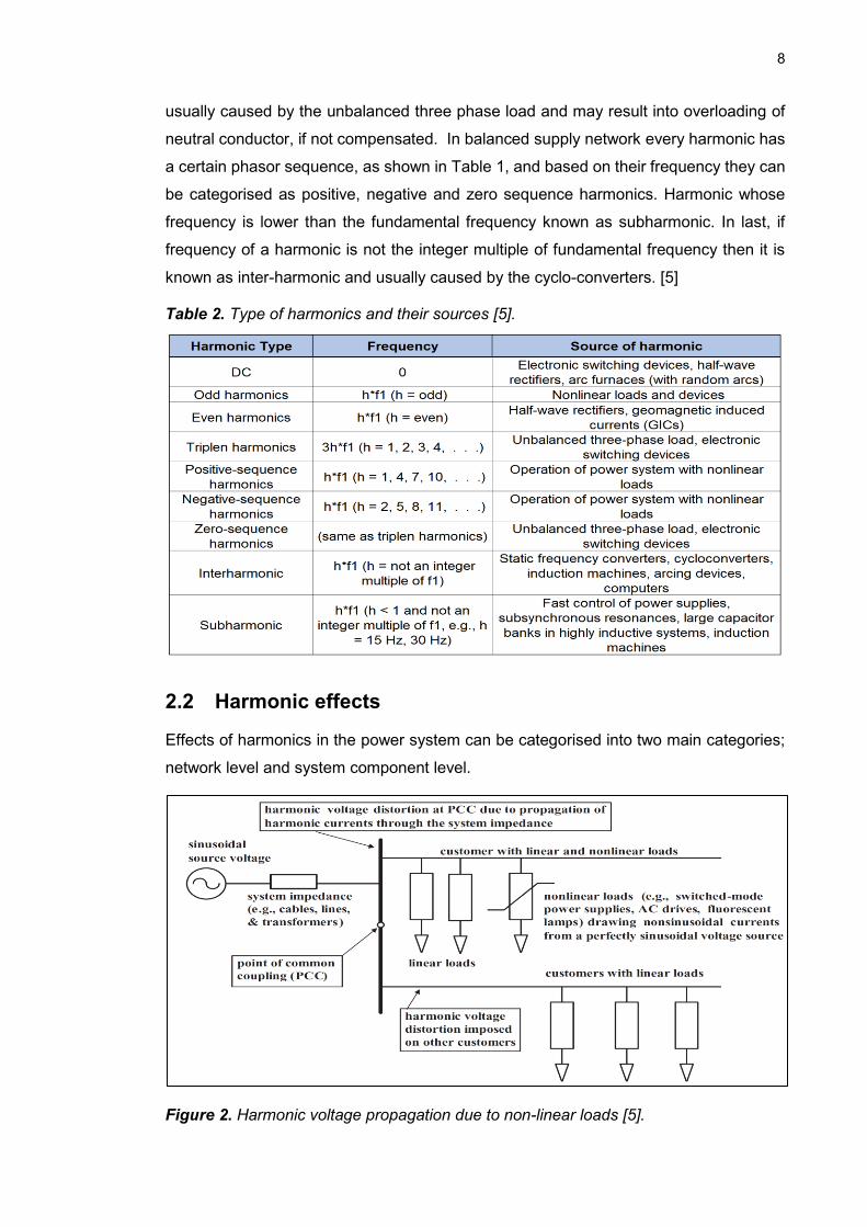
Table 2. Type of harmonics and their sources [5].
Figure 2. Harmonic voltage propagation due to non-linear loads [5].

9
Figure 2. depicts a small network comprising of linear and non-linear loads connected
through the system impendence to a sinusoidal voltage source. Here, non-linear loads
draw a harmonic current from the network. This current while flowing through the system
impedance will cause a voltage drop (harmonic voltage drops to be precise) across the
network. Hence, after subtracting this harmonic voltage drop from the source voltage it
will be noticed that resultant voltage at the point of common coupling (PCC) has become
distorted due to the harmonics. Thus, harmonics caused at the local level (non-linear
load) have the widespread effect (network level) in power system, if no curative step is
taken at the point of origin. For instance, voltage harmonics at the connection point of
motor cause the harmonic fluxes to be produced inside the motor windings. These har-
monic fluxes effect the rotation frequency in a way that motor starts rotating with a fre-
quency other than the synchronous one. Hence, the additional fluxes, caused by voltage
harmonics, produce high frequency currents inside the motor which further results in
additional losses, heating, decreased efficiency and vibration in rotor. [5]
Harmonics have negative impacts on various system components. Speaking of trans-
former, additional heat is the most vital effect caused by the harmonic content available
in the network. This extra heat deteriorates the transformer’s rating to operate within the
defined temperature limit. Moreover, in the presence of harmonics, a transformer’s in-
ductance may cause resonance with the system’s capacitance. [7] Here the concept of
resonance has been explained in detail at the end of this subchapter. Moving further,
Elmoudi et al. [8] suggested that current harmonics contribute to increase in eddy current
and stray losses of the transformer. Distortion in current may cause the protection relays
to trip in unfaulty condition and failing in tripping during a fault [7]. In the case of rotating
machines, harmonics result in increasing the copper and iron losses along with pulsating
torque, which is produced due to the interaction of harmonic and fundamental component
of the magnetic field [9].
As mentioned earlier, in term of phasor rotation with respect to fundamental frequency,
harmonics can be categorised as positive, negative, and zero sequence component.
Each of these harmonic sequences affect the power system differently. Due to same
phaser rotation with the fundamental component, positive sequence harmonics add up
with the fundamental component and result in a composite waveform. Peak to peak value
of this composite waveform might be higher than the peak to peak value of fundamental
waveform alone. Thus, this higher peak to peak value or increased magnitude in general
may contribute in causing the overloading of conductors, transformers and power lines.
[5]

10
On the contrary, due to the opposite rotation with the fundamental component, negative
sequence harmonics give birth to pulsating mechanical torque inside an induction motor.
Being the worst ones, zero sequence harmonics (also known as triplens when system is
balanced) circulate between the phases and neutral (or ground) wire of a three-phase
system. Amount of zero sequence harmonic current in neutral wire is three times higher
than its value in phase wire, since all phase currents coincide in the neutral. Conse-
quently, the main effects due to the zero sequence harmonics are overloading of neutral
conductor and telephone interference. Type of transformer winding connection plays a
big role in preventing the propagation of zero sequence harmonics. For instance, in
“grounded wye-delta” type of transformer zero sequence harmonics enter from the wye
side and due to their nature of zero displacement, they sum up in the neutral conductor.
However, on the other side of the transformer where windings arrangement is in delta
form, these harmonics can enter and flow inside the delta due to its ampere-turn balance
property. But these harmonics remain trapped there and do not appear in the delta side-
line current of the transformer. [5]
Capacitor banks used for the purpose of power factor correction and voltage support
may sometimes contribute to causing harmonic resonance. [10] Capacitor may appear
also from cables, which have high capacitance. Basically, every circuit comprised of ca-
pacitance and inductance may have one or more natural frequency of resonance and
when this frequency matches with the frequency of harmonic current produced by a non-
linear load then amplification of that harmonic current often occurs. Such a phenomenon
of harmonic current amplification due to the system resonance is known as harmonic
resonance. [11] This amplified harmonic current flowing in the network may result in
breaker tripping, blown fuses, audible noises in the capacitor, and disrupting the opera-
tion of neighboring equipment [10].
Harmonic resonance can be further divided into two main types as series and parallel
resonance. Parallel resonance occurs when the system inductance and power factor
correction (PFC) capacitor are in parallel to the harmonic producing source. On the con-
trary, when system inductance and PFC’s capacitance are in series with respect to har-
monic sources, then series resonance occurs. [6] As Eghtedarpour et al. [10] discussed,
in the case of parallel resonance, the net impedance at resonant frequency, seen from
the harmonic source side become very large. Further, multiplying this impedance with
the harmonic current (even small) flowing through the network will cause significant dis-
tortion in voltage. High distortion in voltage will be at the remote point in case of series
resonance and harmonic source (e.g., non-linear load) side in case of parallel resonance
[6]. Traditional solutions to prevent harmonic resonance is to use reactor in series with

11
the PFC capacitor, which further act as a tuned filter circuit [12]. However, the main
problem with such combination of the filter circuit is that it gets de-tuned due to ever
changing dynamics of the system network; change in system impedance caused by net-
work switching, change in load, etc [12].
2.3 Harmonics emission indices and standards
The very essence of harmonic emission calculation is to unfold the mystery of a distorted
waveform in the form of its harmonic and fundamental frequency components. Accord-
ingly, the following formulas have been discussed to provide the reader with enough
mathematical understanding behind harmonic emission measurement before discussing
the standards of limiting harmonics.
Total harmonic distortion (THD) is widely known distortion index for power quality related
issues. It is the ratio of RMS values of all harmonic components available in a signal to
the RMS value of its fundamental component: expressed in percentage. Hence, In terms
of current and voltage, THD can be defined as follows. [4]
𝑇𝐻𝐷voltage(%) = √∑ 𝑉h
2∞h=2
𝑉1∗ 100 (1.4)
𝑇𝐻𝐷current(%) = √∑ 𝐼h
2∞h=2
𝐼1∗ 100 (1.5)
Here, 𝑉h and𝐼h are the RMS value of hth harmonic voltage and current component
wherein 𝑉1 and 𝐼1 refer to the RMS value of fundamental voltage and current component
respectively.
Though THD provides a quicker measurement of distortion as one figure, detailed infor-
mation of signal spectrum is lost. Moreover, it doesn’t incorporate the amplitude infor-
mation of a signal which sometime doesn’t provide the actual insights about how sever
the harmonic emission is. For instance, fundamental current changes depending on the
operating points and therefore, current THD can be very high when the fundamental
current is small. [5]
Considering above mentioned drawback of THD, standards like IEEE-519, further sug-
gested replacing the fundamental component in THD calculation with the RMS value of
rated or load current. Doing so has included the information of varying amplitude too.
Fundamental voltage component doesn’t change much in different network loading con-

12
ditions (e.g. weak network with large load or stiff network with small load) but fundamen-
tal current component varies a lot. Hence, Total Demand Distortion (TDD) is the ratio of
RMS values of all harmonic current components (𝐼h) to the RMS value of the rated cur-
rent (𝐼rated) signal. [4]
𝑇𝐷𝐷(%) = √∑ 𝐼h
2∞ℎ=2
𝐼rated * 100 (1.6)
The relationship between power factor, displacement factor, and THD is one the im-
portant aspect in dealing with harmonic filtering related problems because knowing their
values help in designing various harmonic filter components. Displacement factor (DPF)
is the cosine of angle between current and voltage at the fundamental frequency. It is
the same as the power factor when the waveform is perfectly sinusoidal. [4]
𝐷𝑃𝐹 = cos𝜑1 (1.7)
Here, 𝜑1 is the phase difference between voltage and current at fundamental frequency.
Consequently, power factor (PF) can be defined as follows. [4]
𝑃𝐹 = 𝐼rms−1
𝐼rms∗ cos𝜑1 =
𝐷𝑃𝐹
√1+𝑇𝐻𝐷2 (1.8)
Here, THD is in % and equals to the value of √𝐼rms
2 −𝐼rms−12
𝐼rms−1∗ 100 where 𝐼𝑟𝑚𝑠−1 is the fun-
damental RMS current and 𝐼rms is the total RMS current.
The most widespread and acknowledged power quality standards are from the Institute
of Electrical and Electronics Engineers (IEEE) and International Electrotechnical Com-
mission (IEC). Among these power quality standards, some of them aim to recommend
the practices and guidelines for harmonic control, such as IEEE 519 and IEC 61000
series (e.g., IEC 61000-3-6). [4]
Both IEEE and IEC standards have the recommendation of harmonic limits for the wide
range of voltage levels in a network (e.g., 35kV, 69 kV and 161kV, etc). However, con-
sidering the scope of this thesis, only recommendations for medium voltage (MV), high
voltage (HV) and extra high voltage (EHV) levels, as per their related standards, have
been discussed accordingly.
IEEE 519 -2014, it provides the recommendations of current and voltage distortion limits
along with the indication of how to control the harmonic emission [13]. As part of shared
responsibility, it explains that based on inherent stake of all users, they should limit the
harmonic emission to a reasonable value on their individual level [14]. Moreover, system

13
operators/owners are responsible for restricting the current/voltage distortion while ad-
justing the impedance characteristics of their supplying networks [14].
Table 3. IEEE 519-2014 voltage distortion limits [15].
Table 4. IEEE 519-2014 current distortion limits (69-161 kV) [15].
Table 5. IEEE 519-2014 current distortion limits (above 161 kV) [15].
Prior to discussing the above shown tables, definition/clarification for some of the termi-
nologies is required. Starting with point of common coupling (PCC), it is the nearest elec-
trical point on a supplying network where customer loads are connected or could be
connected. Thereafter, short circuit ratio (Isc/IL) is the ratio of short circuit current (am-
peres) to the load current (amperes), at a particular location. In last, harmonic measure-
ments can be divided into short time meansurement and very short time measurements.
In case of very short time, harmonic measurements are performed with aggregation of
15 cycle over the interval of 3 seconds wherein short time harmonic measurements are
carried out over the interval of 10 minutes while aggregating 200 very short time values
of a certain frequency. [15]
Table 3 represents the voltage harmonic limits at the PCC in percent of the line to neutral
voltage rated at power frequency. Here IEEE 519-2014 further suggests that weekly 95th
percentile of short time harmonic measurement values should be less than the limits

14
shown in Table 3. and daily 99th percentile of very short harmonic measurement values
should be 1.5 times lesser than the values shown in the Table 3. [15]
Table 4 and Table 5 depict the current distortion limits where a user, connected at voltage
level of 69-161 kV and above 161 kV, should restrict the amount of harmonic emission
as: (1) 99th percentile daily very short time measurement values of harmonic current
should be lower than twice the values specified in Table 4 and Table 5, (2) 99th percentile
weekly short time measurement values of harmonic current should be lower than 1.5
times the values mentioned in Table 4 and Table 5, (3) 95th percentile daily short time
values of harmonic current should be smaller than the values specified in Table 4 and
Table 5 for 69-161 kV and above 161 kV connected consumer respectively. [15]
S. M. Halpin [14], further clarifies that as IEEE 519-2014 standard is based on the shared
responsibility concept. Hence, Table 3. shows the voltage distortion limits maintaining
which is the part of system operators’ responsibility. On the other hand, Table 4 and
Table 5 represent the current distortion limits of which to maintain is the part of user/con-
sumer’s responsibility. Interestingly, current distortion limits in Table 4 and Table 5 can
also be referred to individual voltage distortion limits of Table 3. through a system im-
pedance; derived through the short circuit ratio and assuming the value of load current
as 1.0 pu. [14]
The IEC standards have a comprehensive approach in defining harmonic limit criteria for
the utility-customer interface as well as the customer equipment. Speaking of assess-
ment for emission limits in MV, HV, and EHV network systems, IEC/TR 61000-3-6 stand-
ard is widely known. And, since the application of studied STATCOM technology is at
the MV/HV voltage level, therefore this standard has been discussed further in more
detail. However, other IEC standards defining the limits of harmonic current emission for
customer equipment connected to LV and/or public network with different current ratings
(e.g. ≤16, > 16 A and ≤ 75 A) are IEC 61000-3-2, IEC/TS 61000-3-4 and IEC 61000-3-
12. [4]
McGranaghan et al. [16] asserted that unlike other standards, IEC/TR 61000-3-6 pro-
vides guidelines to assess harmonic emission in a network, rather than providing limits
to be met. The main goal of this standard is to guide through the system operators for
carrying out the best engineering practices for ensuring the quality of supply to all con-
nected consumers. [16]
IEC/TR 61000-3-6 standard for voltage distortion is based on the idea of planning and
compatibility levels. Compatibility levels serve the reference values to coordinate with
the immunity and emission of equipment connected at the LV/MV voltage level. However,

15
planning levels can be used to define the limit of harmonic emission in a supplying net-
work, taking into the account presence of all possible harmonic sources. The system
operators define these planning levels for all voltages of the supplying network. Hence,
it can be treated as their internal objectives to deliver the quality of power supply. [17]
Compatibility levels are equal or greater than the planning levels. But planning levels are
defined in a way that they allow the coordination between different voltage levels and
their respective harmonic voltage limits. Having said that, and since different network
structures and operating conditions affect the planning levels, only indicative values
should be assigned. Thus, Table 6 represents the indicative values of planning levels for
voltage distortion at different voltage levels; MV (1 kV < Vnominal ≤ 35 kV), HV (35 kV <
Vnominal ≤ 230 kV) and EHV (230 kV < Vnominal) respectively. Here, harmonic voltage (dis-
tortion) has been shown in the percent of fundamental voltage component for different
harmonic frequencies. [17]
2.4 Mitigation methods
As mentioned earlier, in the last few decades, the number of non-linear loads connected
to the electricity supplying network has been increased drastically and thus caused the
problem of harmonics. Before discussing mitigation methods, one should first under-
stand how harmonics are affected by the different network conditions. In general, with
semiconductor loads, if grid’s strength is strong then it gives high amplitude on the cur-
rent harmonics and lower on the voltage harmonics [18]. Moreover, the amplitude of
harmonic current, for some of the non-linear loads, depends on the effective impedance
of the system (e.g., source impedance + any added line impendence) [19].
Problems caused by harmonics can be eradicated by increasing the level of immunity
for system components, restricting the amount of emission produced by equipment (e.g.,
Table 6. IEC/TR 61000-3-6 indicative planning levels for voltage distortion [17].

16
non-linear loads) and lastly with the help of harmonic mitigation techniques. New har-
monic mitigation technologies along with reformulated and improved classical ones are
available today. Some of the mitigation techniques are based on passive harmonic filters,
active harmonic filters, hybrid harmonic filters, phase shifting transformers and K-factor
transformers, etc. However, considering the scope of this thesis, only passive and active
harmonic filtering method will be discussed further. [20]
2.4.1 Passive harmonic filter (PHF)
Passive harmonic filters are circuits comprised of passive elements (e.g., resistors, in-
ductors, capacitors) which can be arranged in many different orders to serve various
functions (e.g., damping, harmonic filtering, and reactive power compensation, etc). The
main goal of passive filters is to reduce the harmonic level in a network and in some
cases to produce reactive power at the fundamental frequency as well. Based on the
type of connection, PHFs can be categorised as shunt, series and hybrid type with further
subcategory based on the topology of tuned, damped or tuned-damped circuits. Figure
3, represents the family of passive harmonic filters based on their type of connection and
topology. Here, at second level of subcategory, only shunt type PHF is expanded further
due to its wide application and popularity among other harmonic mitigation techniques.
[21]
Figure 3. Passive filters classification based on topology [21].
Shunt harmonic filtering is based on the concept of providing low impedance path to a
harmonic current so that it can be prevented from entering further into the network and
forced to confine through a circuit made of passive elements (e.g., L, C). Among these
passive elements, the capacitor may have negligible internal losses, but this is not the
case with the inductor. Therefore, the inductor is presented with a resistor in series, as
to address its internal power losses. Figure 4 depicts the various type of shunt passive
filters wherein Figure 4(a) represents the single tuned or notch filter, tuned at a particular
frequency of filtering (e.g., 150 Hz). It is a simple RLC series circuit where capacitor and

17
inductor values are driven through the amount of reactive power needed and value of
tuned frequency, respectively. Moreover, value of resistance R defines the sharpness of
filter and limit the amount of harmonic current flowing through the filter. Double or multi
tuned circuits can be made while combining two or more single tuned filters in a circuit,
as shown in Figure 4(b). [21]
Figure 4. Shunt passive: (a) single tuned, (b) double tuned, (c) first order, (d) second
order, (e) C-type. Series passive: (f) single tuned. Hybrid passive: (g) combination of
passive series filter (𝑷𝑭𝒔𝒔) and passive shunt filters (𝑷𝑭𝒔𝒉) [21].
High-pass filters (HPF) are used to prevent the flow of high order harmonics (at least 2-
4 different order harmonics) in the system. Due to the presence of resistor, these filters
can provide the damping and thus they are also known as damped filters. However,
presence of resistor not only restrict the filtering limit of the filter but also increases its
losses. As shown in Figure 4(c), first-order high pass filters are simple RC circuit which
can be used to regulate the voltage at PCC even in the presence of high order harmon-
ics. Second-order high pass filters, depicted in Figure 4(d), are often used in the system
since they come with better harmonic filtering and damping characteristics. HPF compo-
nents are less affected by the temperature and frequency variation and therefore tend
not to get detuned easily. Structure of the C-type filter is similar to second-order HPFs
except for the added second capacitor C2 in series with inductor L, as shown in Figure
Figure 4(e). Here, the series combination of second capacitor and inductor form reso-
nance at the fundamental frequency, hence, preventing the flow of fundamental current
through the resistor and therefore minimising losses. However, if resonance circuit of L
and C2 is tuned to higher frequency, losses might increase. [21]
As shown in Figure 4(f), unlike shunt, series passive filters are the parallel arrangements
of passive components (e.g., inductor, capacitor, etc.) connected in series with a supply-
ing network or a harmonic producing load requiring harmonic filtering. A series passive
filter offers low impedance to the current component at the fundamental frequency,
hence allowing it to flow through the circuit with negligible voltage drop. But it offers high
(a) (b) (c) (d) (e)
(f)
(g)

18
impedance to the harmonic components and thus blocking their flow through the circuit.
Series passive filters are used to filter a particular harmonic current, such as third har-
monic. Due to the series connection, these filters need to carry full rated load current,
which may restrict their application to single-phase low power rating equipment/networks
only. Moreover, they consume reactive power (lagging) at a fundamental frequency
which causes a voltage drop in the network and proven to be a downside of series har-
monic filters. [21]
Considering drawbacks of both series and shunt passive filters, one possible way is to
put them together in the certain configurations which offers the best performance. Such
a combined configuration, as presented in Figure 4(g), is referred to a hybrid passive
filter. Single-tuned series passive filter’s drawback of absorbing reactive power, when
implemented in hybrid filter, can be utilised in consuming the excess reactive power gen-
erated by a shunt passive filter under the light loading conditions. Moreover, series pas-
sive filter can also help in blocking the resonance occurring between the supplying sys-
tem and a shunt passive filter. [21]
J. C. Das [22] argued that though PHFs have potential of being maintenance-free, scal-
able in size (large MVars and power), cost-effective and possibly faster response of one
cycle or less when implemented with SVC, they also come with significant limitations.
PHFs are rigidly placed, and therefore, their tuning frequency and filter’s size can not be
changed. Given this situation, PHFs are not a good option for changing system condi-
tions. These changing conditions may even result in detuning of the filters. Apart from
sporadic system conditions, detuning can happen due to increase in designed tolerance
limit; further caused by the aging, temperature, and deterioration. Effective design of
passive filters is largely affected by the system impedance and may even cause a prob-
lem in the stiff network. Stepless control of filter for reactive power control in changing
load conditions is not possible; either it can be switched on or off. [22] Resistive compo-
nent of the filter may cause losses in large size application. In last, a parallel resonance
between the filter’s capacitance and line inductance may cause the harmonic amplifica-
tion in the system [21].
2.4.2 Active harmonic filter (AHF)
To overcome the drawbacks of passive filters for being fixed in size and compensation,
problems of resonance, detuning, etc., there was a need to look for other harmonic mit-
igation techniques. Thanks to the growing field of power electronics, it was possible to
develop dynamic and adjustable harmonic filtering solutions. These solutions are known
as active harmonic filters (AHFs) if only used for harmonic compensation. But if they
19
serve multiple purposes, such as harmonic compensation, reactive power compensa-
tion, load balancing, voltage flicker mitigation, etc., then they are well known as active
power line conditioners (APLCs). [23]
Based on topology AHFs can be classified as series, shunt and hybrid filters wherein
connection with the power supply may vary from case to case or depending upon the
filter’s application (e.g., Single phase-2 wire, Three phase- 3 or 4 wire, etc.). AHFs have
gone through tremendous development based on the breakthrough in power electronic
switches technology, system and control techniques, microelectronics, and converter de-
sign. The essential components of an AHF are passive elements (e.g., inductor, capac-
itor), power electronic switches and its control system. Speaking of power electronic
technology, AHFs are made of different switches such as bipolar junction transistor
(BJT), metal oxide semiconductor field effect transistor (MOSFET), gate turn-off thyristor
(GTO), insulated-gate bipolar transistor (IGBT), integrated gate-commutated thyristor
(IGCT), etc. Some of the control strategies are instantaneous reactive power theory,
synchronous frame theory, hysteria control, etc. [23] Part of controller devices for AHFs
started with discrete signal and later got shifted to digital signal processor based tech-
nologies [24], [25]. To incorporate the dynamic and steady performance of AHFs for spo-
radically changing system conditions, complex algorithms for real-time control are devel-
oped and further supported by the improvement in control platforms of proportional inte-
gral, fuzzy logic, variable structure and neural network-based controls [26]–[28].
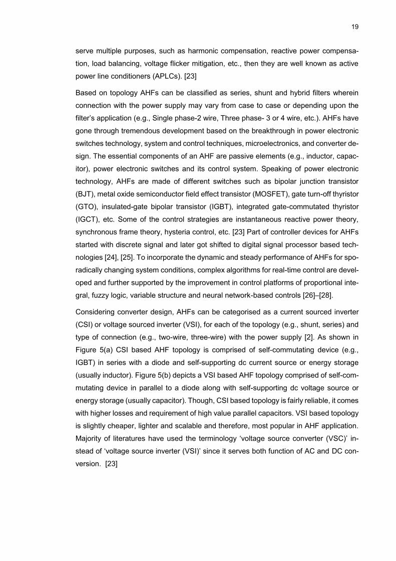
Considering converter design, AHFs can be categorised as a current sourced inverter
(CSI) or voltage sourced inverter (VSI), for each of the topology (e.g., shunt, series) and
type of connection (e.g., two-wire, three-wire) with the power supply [2]. As shown in
Figure 5(a) CSI based AHF topology is comprised of self-commutating device (e.g.,
IGBT) in series with a diode and self-supporting dc current source or energy storage
(usually inductor). Figure 5(b) depicts a VSI based AHF topology comprised of self-com-
mutating device in parallel to a diode along with self-supporting dc voltage source or
energy storage (usually capacitor). Though, CSI based topology is fairly reliable, it comes
with higher losses and requirement of high value parallel capacitors. VSI based topology
is slightly cheaper, lighter and scalable and therefore, most popular in AHF application.
Majority of literatures have used the terminology ‘voltage source converter (VSC)’ in-
stead of ‘voltage source inverter (VSI)’ since it serves both function of AC and DC con-
version. [23]
20
Figure 5. Active Filter: (a) CSI based- current fed, (b) VSI based- voltage fed [23].
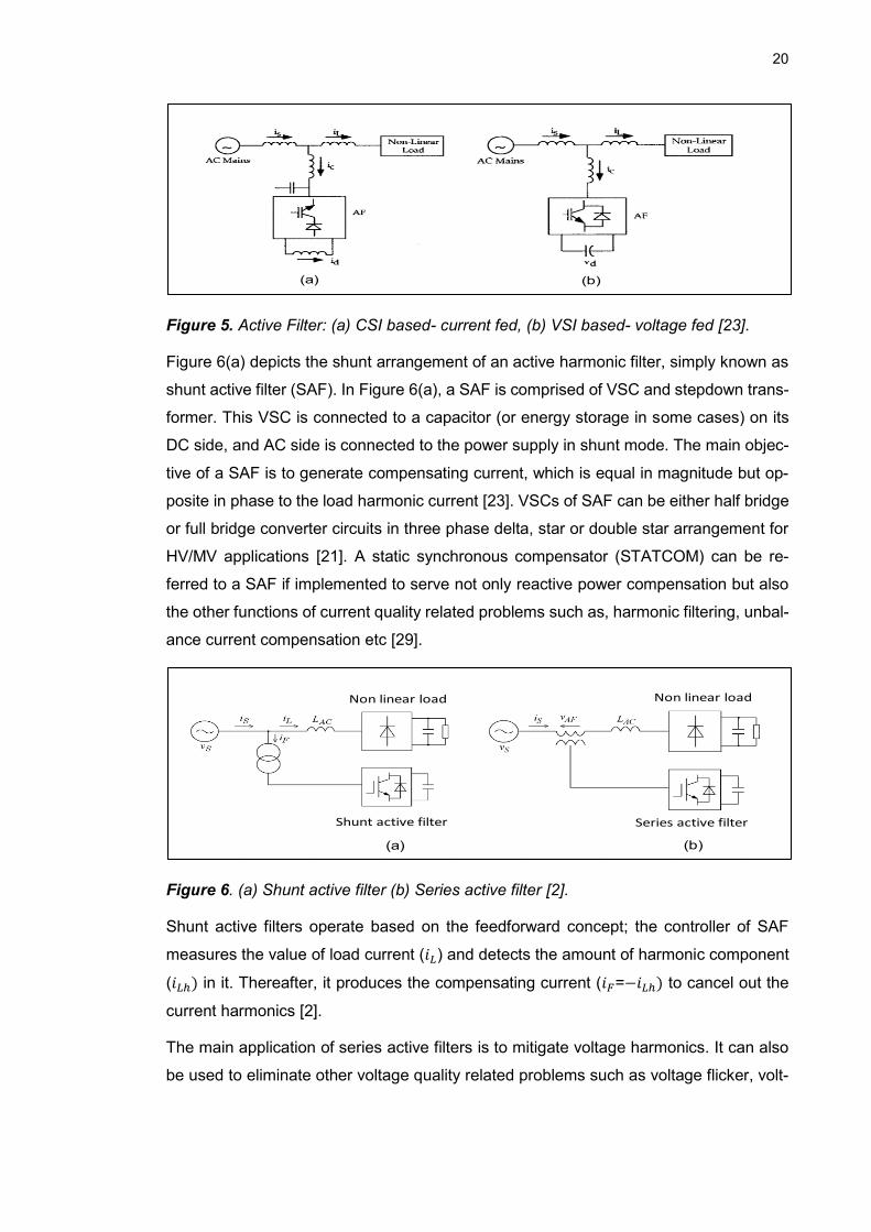
Figure 6(a) depicts the shunt arrangement of an active harmonic filter, simply known as
shunt active filter (SAF). In Figure 6(a), a SAF is comprised of VSC and stepdown trans-
former. This VSC is connected to a capacitor (or energy storage in some cases) on its
DC side, and AC side is connected to the power supply in shunt mode. The main objec-
tive of a SAF is to generate compensating current, which is equal in magnitude but op-
posite in phase to the load harmonic current [23]. VSCs of SAF can be either half bridge
or full bridge converter circuits in three phase delta, star or double star arrangement for
HV/MV applications [21]. A static synchronous compensator (STATCOM) can be re-
ferred to a SAF if implemented to serve not only reactive power compensation but also
the other functions of current quality related problems such as, harmonic filtering, unbal-
ance current compensation etc [29].
Figure 6. (a) Shunt active filter (b) Series active filter [2].
Shunt active filters operate based on the feedforward concept; the controller of SAF
measures the value of load current (𝑖𝐿) and detects the amount of harmonic component
(𝑖𝐿ℎ) in it. Thereafter, it produces the compensating current (𝑖𝐹=−𝑖𝐿ℎ) to cancel out the
current harmonics [2].
The main application of series active filters is to mitigate voltage harmonics. It can also
be used to eliminate other voltage quality related problems such as voltage flicker, volt-
(a) (b)
Non linear load Non linear load
Shunt active filter Series active filter
(a) (b)
21
age sag, voltage unbalance, etc. Series active filters, as shown in Figure 6(b), are con-
nected in series with the supplying network and/or before the load through a transformer
and they produced the required amount of voltage component to cancel out the network
harmonic voltages. Like shunt active filters, they can also be categorised based on con-
verter circuits (e.g. CSI or VSI) and type of connection (e.g., 2-wire, 3-wire, 4-wire, etc.)
with power supply. [30]
Unlike shunt active filters, control strategy of series active filters is based on the concept
of feedback; controller measures the instantaneous value of supplying current (𝑖𝑆) and
separates the harmonic component (𝑖𝑆ℎ) value from the net supplying current. Using this
harmonic current component(𝑖𝑆ℎ) and adequate feedback gain(𝐾) value, series active
filter calculates the needed amount of compensating voltage (𝑣𝐴𝐹 = −𝐾 ∗ 𝑖𝑆ℎ). Thereaf-
ter, applying this compensating voltage at the primary side of connecting transformer
results into decreasing the current harmonics and consequently a reduction in net volt-
age harmonics as well. [2]
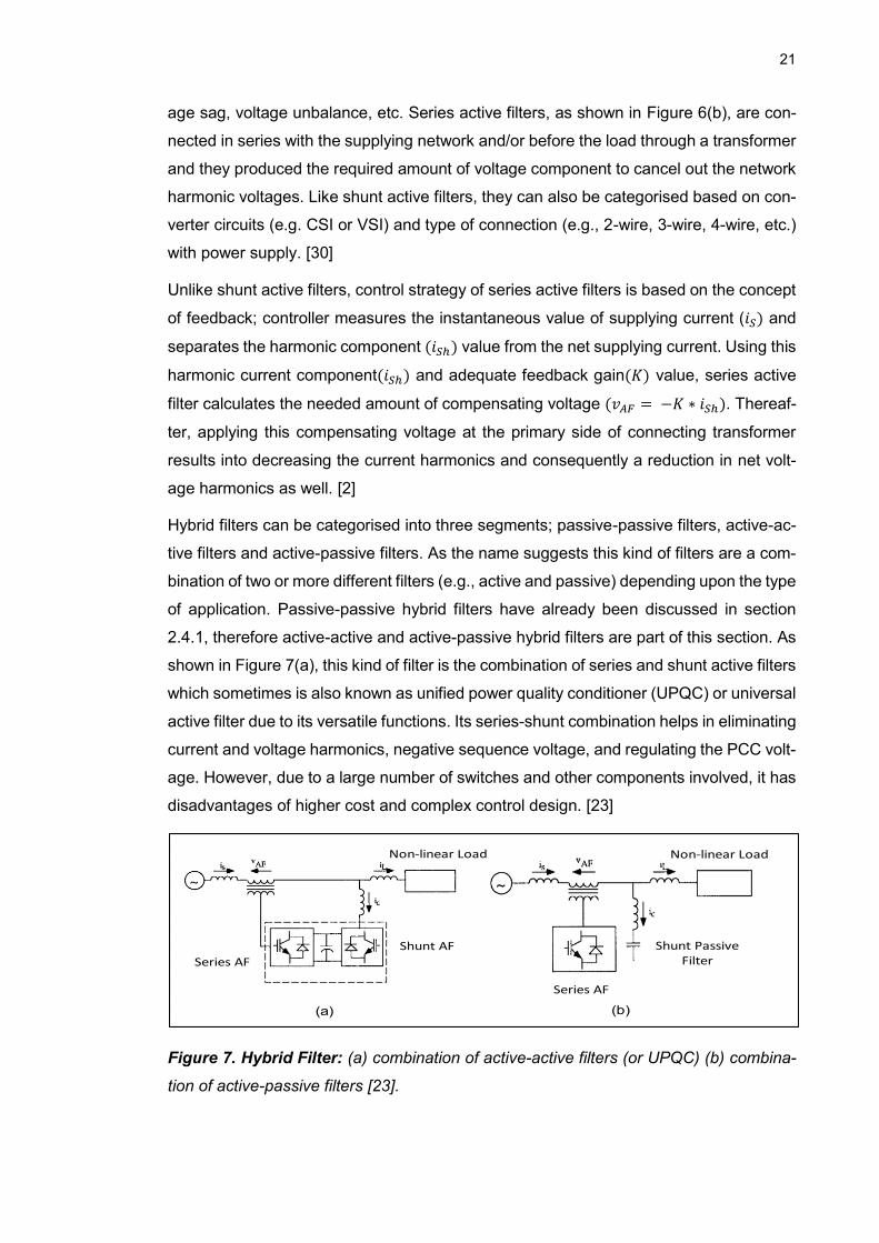
Hybrid filters can be categorised into three segments; passive-passive filters, active-ac-
tive filters and active-passive filters. As the name suggests this kind of filters are a com-
bination of two or more different filters (e.g., active and passive) depending upon the type
of application. Passive-passive hybrid filters have already been discussed in section
2.4.1, therefore active-active and active-passive hybrid filters are part of this section. As
shown in Figure 7(a), this kind of filter is the combination of series and shunt active filters
which sometimes is also known as unified power quality conditioner (UPQC) or universal
active filter due to its versatile functions. Its series-shunt combination helps in eliminating
current and voltage harmonics, negative sequence voltage, and regulating the PCC volt-
age. However, due to a large number of switches and other components involved, it has
disadvantages of higher cost and complex control design. [23]
Figure 7. Hybrid Filter: (a) combination of active-active filters (or UPQC) (b) combina-
tion of active-passive filters [23].
Series AF
Shunt AF
Non-linear Load
Series AF
Shunt Passive Filter
Non-linear Load
(a) (b)

22
In case of active-passive filter based hybrid topologies, different arrangements can be
made using (1) Series AHF and Shunt PHF, (2) Shunt AHF and Shunt PHF, (3) Series
AHF in series with Shunt PHF, etc. [31]-[33]. The most popular arrangement is series
AHF and shunt PHF based hybrid filter, as shown in Figure 7(b). It comes with reduced
cost, in comparison to purely active filter-based solutions because majority of harmonic
compensation part of the unit is taken care by the passive filters (usually for low order
harmonics). [23] Here active filter plays the role of a harmonic isolator between the load
and source side, hence, forcing harmonics to shunt passive filter and letting them confine
through it [2].
In conclusion, it is hard to argue whether pure active filters (e.g., active-active) or hybrid
active filters (e.g., active-passive) are the best solutions for harmonic filtering because
choosing one is based on the trade-off between cost and performance. Pure active filters
come with higher cost and a rather versatile functions of power conditioning (e.g., reac-
tive power control, load balancing, harmonic mitigation, etc.) but hybrid active filters are
more effective if used for harmonic filtering only. [2]

23
3. REACTIVE POWER COMPENSATION (RPC)
Like harmonics, reactive power also poses severe threats to the power system. Majority
of power quality issues are influenced by the presence of unwanted reactive power and
can be resolved if adequate compensation techniques put into the place. Capacitor and
reactor store the reactive power generated by an AC source in the quarter of the funda-
mental cycle and transfer it back to the source in the next quarter of the fundamental
cycle. Hence, the oscillation of reactive power occurs between the AC source and ca-
pacitor or reactor (or other devices which utilise reactive power for producing magnetic
field; motors) at twice the frequency of fundamental cycle in an AC system (e.g. 100 Hz
for 50 Hz rated system). [31]
Categorically reactive power compensation may serve two main objectives; load balanc-
ing and voltage support. Load balancing attributes to improve system power factor,
amount of real power drawn, and mitigating harmonics produced by the non linear load.
In case of voltage support, reactive power is used to alleviate the voltage fluctuation at
a certain network point (e.g. PCC) and thus maintaining a flat voltage profile. [31] More-
over, efficient reactive power compensation enables the economical dispatch of real
power [32]. Some of the reactive power compensation techniques, based on the mature
technology, can be dived into the three main segments as (1) Passive Var compensation
(e.g. series and shunt capacitor/reactor), (2) Rotating synchronous Var compensator
(e.g. synchronous condenser) (3) FACTS based solutions (e.g. SVC, STATCOM, UPQC,
etc.) [31]. However, keeping the objectives of this thesis into consideration, only shunt
based passive and FACTS Var solutions have been outlined in the following subchap-
ters, with more emphasis on the STATCOM technology.
3.1 Passive Var compensation
Passive Var compensators are made of reactive elements such as reactor and capaci-
tors, connected in series or shunt configuration with the power supply. The main objec-
tive of series compensation is to alter the network’s parameters (e.g. voltage, current)
wherein shunt compensation is used for changing the load side impedance. But using
both scenarios, effective control of reactive power flow can be carried out. [31]
Classification of passive Var compensators based on the topology can be summarised
as shunt, series, and hybrid compensators. Further, they can be divided based on the
number of phases such as two-wire, three-wire, or four-wire compensators. The series

24
topology of passive Var compensators has a limited implementation in electricity network
due to their impact on the performance characteristic of load and tendency to create
series resonance. Their main application is in transmission network to shorten its length
(with decreased voltage drop) and thus to provide improved power transfer capability.
On the other hand, shunt topology doesn’t affect the operation of load much and there-
fore proven to be more effective passive Var solution when compensation is needed at
the load side. But they are also widely used in the power distribution network for voltage
regulation. [21]
Figure 8. (a) Network without compensation, (b) Network with shunt Var compensation,
(c) phasor of network without compensation, (d) phasor of network with compensation
[21].
Figure 8 demonstrates the fundamental principal behind shunt compensation technique.
In Figure 8(a), an inductive load (𝑍L) is feeding through a power source (𝑉S). Since load
is inductive, hence it’s drawing reactive (𝐼𝑄) and active current (𝐼𝑅) from the source for its
effective operation. Due to this reactive current, amount of resulted current has in-
creased, and when flowing through the system impedance, it will cause more losses in
the form of voltage drop. However, flow of this reactive current can be prevented if it can
be supplied locally (e.g., near to load) with the following designing strategy [21].
Figure 8(a) and Figure 8(c) shows the case of single-phase inductive load without Var
compensation. Therefore, supply/load current can be computed as:
𝐼s = 𝐼L =𝑉L
𝑍L= 𝑉L(𝐺L + 𝑗𝐵L) = 𝐼R + 𝑗𝐼Q (3.1)
δ
𝑰 𝑰 = 𝑰
𝑰
𝑰 𝑰
𝑰 = 𝑰
𝑰𝒔 𝒔
𝑰
𝑰
(a) (b)
(c) (d)

25
Here, 𝐼R is active component of source current and in phase with the load voltage 𝑉L
wherein 𝐼Q is the reactive component of source current and in quadrature with the load
voltage.
Apparent power of the load:
𝑆L = 𝑃L + 𝑗𝑄L = 𝑉L ∗ 𝑉L(𝐺L − 𝑗𝐵L) = 𝑉L2(𝐺L − 𝑗𝐵L) (3.2)
From equation 3.1 and 3.2 it can be concluded that if we connect a compensator having
admittance value of −𝑗𝐵L(capacitive), it will produce a current of 𝐼C = −𝑗𝑉L𝐵L (opposite
to 𝐼Q)
Now the supply current post compensation, using Figure 8(b), will be.
𝐼s = 𝐼L + 𝐼C = 𝑉L(𝐺L + 𝑗𝐵L) − 𝑗𝑉L𝐵L = 𝑉L𝐺L = 𝐼R (3.3)
Needed rating of compensator
𝑆C = 𝑃C + 𝑗𝑄C = 𝑉L ∗ 𝐼C∗ = 𝑉L ∗ (−𝑗𝑉L𝐵L)
∗ = 𝑗𝑉L2𝐵L (3.4)
Here, PC will be zero, since we only need reactive power (capacitive in this case).
Hence, shunt compensator produces the equal amount of reactive current (but in oppo-
site phase (180°) to cancel out the reactive current demand of inductive load from the
main supply. Doing so results into making the net supplying current purely resistive (𝐼s =
𝐼R). This current when flowing through the system impedance causes less losses and
thus improved voltage profile at the load side, as depicted in Figure 8(d). [21]
Reactive power compensation in shunt mode can be carried out in three possible way:
(a) current-source, (b) voltage-source or (c) capacitor/inductor, Var generators. Voltage
or current source-based shunt compensation methods (e.g., STATCOM) have been dis-
cussed in the latter part of this thesis. Reactive power generated by current or voltage
sourced Var generators is independent of the voltage at the point of connection, if same
is operating within the defined Var limit. However, this is not the case with capacitor (or
inductor) based compensators because of the following reason. [31]
𝑄cap = 𝑉 ∗ 𝐼cap 𝑜𝑟 𝑉2
𝑋cap (3.5)
Here, 𝑄cap is the amount of reactive power generated, 𝐼cap is the reactive (capacitive)
current, 𝑉 is the voltage at the point of connection and 𝑋cap is the value of reactance for
capacitor. For inductive load, reactive power generated by the shunt compensator will
be capacitive and inductive in case of capacitive load. However, it can be inferred from
equation 3.5 that the amount of reactive power generated/absorbed by a shunt compen-
sator is proportional to the square of connection point voltage. So, changing in system

26
voltage will result in significant variation of generated/absorbed reactive power by the
compensator, and thus, the load either will be under-compensated or over-compensated.
Fixed shunt passive compensators are not the best solutions under changing system
conditions. But controllability over Var generation/absorption can be achieved if used
capacitors/inductors are equipped with the electromechanical switches. With the help of
relay and circuit breakers, the number of capacitors/inductors inside the compensation
circuit can be switched in or out depending on the requirement of total Var. The probable
consequences of using mechanically switched passive compensators will be the slow
and erratic control, the possibility of high inrush current and need of frequent mainte-
nances. In last, considering total cost, they are rather cheaper in comparison to modern
FACTS based solutions. [33]
3.2 SVC
Static Var Compensator (SVC) is a shunt linked thyristor-controlled Var (i.e., leading or
lagging) generator. Due to the presence of thyristors, it has been given the name “Static.”
The main application of SVC is to maintain its coupling end network (HV/MV) voltage to
a predefined reference value. Apart from voltage control, other functions of SVC are re-
active power control, power oscillation damping, and load balancing. SVC is one of the
members of FACTS family; preliminary used for increasing the system’s transferability
and controllability in term of power flow and thus improving its stability. [34]
Though the design of SVCs may vary from case to case, its main components are Thy-
ristor Controlled Reactors (TCR), Thyristor Switched Capacitor (TSC), harmonic filters,
stepdown transformer and sometimes mechanically switched reactors or capacitors too.
A typical arrangement of these components for HV/MV SVC application can be repre-
sented through the configuration shown in Figure 9. [35]

27
Figure 9. A general SVC configuration [35].
TCR is the combination of anti-parallel thyristors connected in series with a linear air-
core reactor. These thyristors act like a switch while one of them conducting in the posi-
tive half cycle and another in the second half cycle of the mains supply. The conducting
mechanism of the thyristor is controlled by its firing angle; measured through zero cross-
ing value of the voltage across the thyristor’s terminals. This firing angle varies from 90°
to 180° wherein 90° contribute to full conduction of thyristor and 180° being the angle of
no conduction at all. Varying the fire angle values in between 90° and 180° enables TCR
current to flow in the form of discontinuous pulses, symmetrically placed in both positive
and negative half cycle of AC power supply. However, to better understand such behav-
ior of TCR current, the following equation has been worked out. [36]
𝐼TCR = 𝑉s ∗ 𝐵TCR (3.6)
From equation 3.6, it can be implied that since the applied voltage is constant, the
amount of fundamental current (reactive current) for a TCR is directly proportional to its
susceptance. But this susceptance further depends on the firing angle of thyristors, which
means varying the firing angle will result in the variation of susceptance and conse-
quently adequate variation in the reactive current of TCR. [36]
Grid Connection (e.g. PCC)
Stepdown Transformer
MechanicallySwitched Reactor
Thyristor Controlled Reactor (TCR)
Thyristor Switched Capacitor
(TSC)
Harmonic Filter
(e.g. 5th, 7th)
MechanicallySwitched Capacitor

28
Thyristor Switched Capacitor (TSC) also comprises of antiparallel thyristors valve in se-
ries with a capacitor and an inductor. But in TSC, thyristor’s conduction control is not
based on the variation of firing angle, so, either they are switched ON with full conduction
or remains switched OFF. It means the output current of TSC is purely sinusoidal in
steady-state condition. [31]
Figure 10. SVC’s V-I characteristics
In voltage regulation, SVC’s susceptance is varied to achieve the desired voltage level
at PCC. As represented in Figure 10 of V-I characteristics, a SVC can maintain the con-
stant voltage at a given reference value (Vref) while varying the output current (driven
from variation in susceptance) over its range of controllability (𝐵TSC(Cmax) < 𝐵SVC <
𝐵TCR(Lmax)) [37]. Outside its controllable range, SVC behaves like a capacitor during un-
dervoltage condition and like an inductor during overvoltage conditions [38]. Hence, the
amount of reactive power generated or absorbed in such conditions follows equation 3.5,
as mentioned earlier.
Incorporating slope in SVC characteristic comes with the advantages of a significant re-
duction in its power rating, enabling parallel operation with other compensators to
achieve cost-effective controlling objective and finally, slope helps in preventing SVC to
reach its maximum operating limits quite frequently. [38]
Grigsby et al. [38] have suggested that SVC is more effective in voltage control operation
when short circuit impedance of the system is quite high (e.g., weak grid) but its control-
ler’s response becomes sluggish in strong grid conditions. Mathur et al. [39] have rightly
argued that there is no single configuration (e.g., FC-TCR, MSC-TCR, TSC-TCR, etc.)
of SVC, which offers the best reactive power compensation solution. But considering,
Voltage
Reactive current
Capacitive Inductive
BTCR(Lmax)
BTSC(Cmax)
VrefSlope

29
operational frequency, response time, losses, capital cost, and other factors, “TSC-TCR”
based SVC configuration is the most viable option [36].
3.3 STATCOM
The other important member of FACTS family is the static synchronous compensator
(STATCOM). The primary aim of STATCOM is to provide the dynamic and fast reactive
power compensation support to a network at the point of its coupling. [31] However, since
it is a power conditioning device, hence, it can be implemented to solve other power
quality related issues as well, such as harmonic filtering, load balancing, power oscilla-
tion damping, voltage regulation, etc. [2].
Like SVC, STATCOM is also a shunt connected compensation device, but its structure
and operational principle differ from the SVC. Speaking of structure, STATCOM is a con-
verter-based circuit, connected in parallel to the network through its coupling reactor and
acting like a controllable voltage source. It is analogous to a synchronous machine in
term of generating sinusoidal voltage with the fundamental frequency and freedom to
control amplitude and phase-angle at its output. [31]
Since STATCOM is a self-commutated converter-based device and its generated reac-
tive power is proportional to the PCC voltage, therefore it can generate one p.u. of reac-
tive power even in significantly undervoltage conditions. On the other hand, thyristor-
based devices like SVCs are not capable of doing the same because their shunt con-
nected capacitor or reactor’s current capability is proportional to PCC voltage squared.
Moreover, STATCOMs are smaller in size comparing to SVCs due to almost no require-
ment of passive elements and therefore have small footprints. Further, self-commutated
converters offer a quick response which enables a STATCOM to control the reactive
power faster and more precisely. Due to the modern power electronic switches (e.g.,
IGBT, IGCT), different converter topologies (e.g., modular multilevel converter), ade-
quate control and modulation techniques, STATCOMs have been able to offer plenty of
benefits. For example, lower harmonics emission, short term transient overloading ca-
pability, parallel power conditioning operations (e.g. harmonic filtering) and no inrush
current generation etc. But some of the shortcomings of STATCOM, such as high capital
cost and intricate control design, put it behind the SVCs, in term of world-wide implemen-
tation or popularity. [34]

30
3.3.1 Operation principle
Figure 11(a) depicts the single line diagram of a STATCOM. The main components of a
STATCOM can be summarised as the DC capacitors, voltage source converters (VSC),
coupling reactors, and a stepdown transformer. DC capacitor sometimes can be re-
placed with a DC energy source, if active power support from the STATCOM is also
needed (e.g., application in wind farm). The main function of a capacitor is to provide
constant DC voltage to the VSC, which is further connected in shunt mode with the mains
supply through a coupling reactor and a stepdown transformer. A STATCOM can be
viewed as a synchronous machine acting like a controllable voltage source behind the
coupling reactance. [38]
Figure 11. STATCOM: (a) Single line diagram, (b) Standby mode, (c) Inductive mode,
(d) Capacitive mode [38], [39].
Reactive power compensation using a STATCOM is based on the concept of voltage
amplitude difference. According to which, if STATCOM voltage (𝑉c) is higher than the
connection point voltage (𝑉s) then a current (𝐼STATCOM) flows from the STATCOM to the
connection point (e.g., PCC) and thus causes the generation of capacitive reactive
power, shown in Figure 11(d). On the contrary, if 𝑉c is lower than 𝑉s then current flows
from the connection point to STATCOM and causes the absorption of inductive reactive
power, shown in Figure 11(c). However, if 𝑉c and 𝑉s both are equal in amplitude, then
there will be no flow of current from either side. Thus, STATCOM will remain in standby
mode as shown in Figure 11(b). [38]
𝒕𝒊 𝒊𝒕 ( 𝒔)
( )
𝑰 = 𝟎
CouplingReactor ( )
Voltagesource
converter(VSC)
𝑰 (𝑰)
(a)
(c)
(d)
(b)

31
To better understand the above stated fact, let’s take the example of a STATCOM (𝑉𝑐)
connected to the utility supply point (𝑉s) through a coupling reactor 𝑋L as depicted in
Figure 11(a).
STATCOM current:
𝐼STATCOM = (𝑉s − 𝑉c)/𝑗𝑋L = (𝑉s − 𝑉c∠ − 𝜃)/𝑗𝑋L = (𝑉c 𝑠𝑖𝑛 𝜃 − 𝑗(𝑉s − 𝑉c 𝑐𝑜𝑠 𝜃))/𝑋𝐿 (3.7)
Here, 𝐼STATCOM is the STATCOM current and 𝜃 is the phase angle of STATCOM voltage
w.r.t to supply voltage.
Apparent, active and reactive power of the STATCOM:
𝑆STATCOM = 𝑉s ∗ 𝐼STATCOM∗ = 𝑉s ∗ ((𝑉c 𝑠𝑖𝑛 𝜃 − 𝑗(𝑉s − 𝑉c 𝑐𝑜𝑠 𝜃))/𝑋L )
∗ (3.8)
𝑆STATCOM = 𝑃STATCOM + 𝑗𝑄STATCOM = (𝑉s𝑉c 𝑠𝑖𝑛 𝜃 + 𝑗(𝑉s2 − 𝑉s𝑉c 𝑐𝑜𝑠 𝜃))/𝑋L (3.9)
𝑃STATCOM = (𝑉s𝑉c 𝑠𝑖𝑛 𝜃)/𝑋L (3.10)
𝑄STATCOM = (𝑉s2 − 𝑉s𝑉c 𝑐𝑜𝑠 𝜃)/𝑋L (3.11)
From equation 3.10, it can be noticed that while varying the phase angle between STAT-
COM and connection point voltage, active power exchange can be controlled. However,
considering STATCOM application for only reactive power compensation-based opera-
tions, we can assume that its active power exchange with the system is zero (if neglect-
ing the losses); which is only possible when STATCOM and connection point voltage
both are in phase (mean 𝜃 = 0).
Therefore,
𝑃STATCOM = (𝑉s𝑉c sin0°)/𝑋𝐿 = 0 (3.12)
𝑄STATCOM = (𝑉s2 − 𝑉s𝑉c cos 0°))/𝑋L = (𝑉s
2 − 𝑉s𝑉c)/𝑋L (3.13)
Now, equation 3.13 concludes that if the magnitude of generated STATCOM voltage (𝑉𝑐)
is higher than the connection point voltage (𝑉s) then reactive power flows from the STAT-
COM to connection point (negative sign of 𝑄STATCOM; capacitive power). On the contrary,
if 𝑉c is lower than (𝑉s) then reactive power flows from connection point to STATCOM
(positive sign of 𝑄STATCOM; inductive power).
Reactive power exchange of the STATCOM is enabled by the mechanism of input and
output power of its converter (e.g., VSC). The converter is comprised of power electronic
switches which directly connect the DC side of a STATCOM to its AC side output. Hence,
if we neglect the losses, then the amount of instantaneous power should be equal at both
of its AC and DC terminals. Active power provided by the DC source, as an input to the
converter, will be zero if we assume that the converter is only responsible for reactive

32
power exchange. Also, DC source doesn’t directly contribute to reactive power genera-
tion at the converter’s output terminal. But it is the combined operation of DC source and
switches with adequate control technique which connects the VSC’s output terminal in a
way that reactive currents circulate among the terminal phases and establish the reactive
power exchange with the system. [38]
To establish reactive power exchange, DC capacitor voltage should remain fairly con-
stant throughout the STATCOM operation. But losses within the converter cause the
capacitor voltage to drop. These losses arouse mainly due to the switching of power
electronic devices. Therefore, to maintain the required constant DC voltage, these losses
should be feed from the AC mains. Additionally, some STATCOM applications are to
provide both real and reactive power support. In such applications, DC source used at
the converter side is a battery or energy storage (with a significant amount of active
energy) which enables the real power support operation of a STATCOM during various
network contingencies (e.g., faults, loss of mains, etc.). The exchange of real power be-
tween STATCOM and AC mains can be enabled while varying the phase angle between
STATCOM voltage and connection point voltage. If STATCOM voltage is made to lead
from the connection voltage, then the flow of real power will be from STATCOM to the
AC mains. But if STATCOM voltage is made to lag by the connection point voltage, then
real power will flow from AC mains to the STATCOM. [40], [41]
As depicted in Figure 12 of V-I characteristics, while participating in the reactive power
compensation, a STATCOM can control its output current over the rated maximum ca-
pacitive and inductive range, irrespective to the system voltage. Because, it has the
same current rating in both capacitive and inductive region which means certain MVA of
a VSC provides the double dynamic range of MVAr to STATCOM. Further, it signifies
that a STATCOM can produce continuous maximum capacitive current even with as low
voltage as 0.15 pu. A STATCOM can be an effective solution when voltage support is
required during the fault or post fault conditions, especially when low voltage or sudden
voltage collapse create the bottleneck for other compensation devices (e.g., PHFs,
SVCs). The dotted region in Figure 12 represents the increased transient limit of a STAT-
COM in both capacitive and inductive region, but operation here requires a pay-back
time otherwise DC link voltage of STATCOM may vary. In the capacitive region, transient
overcurrent is limited by the maximum turn-off capability of VSC’s switches (e.g., IGBT)
and in inductive range, it is limited by the maximum junction temperature of the switches.
[36]

33
Figure 12. STATCOM’s V-I characteristics [42].
The most vital part of a STATCOM is its converter. There are mainly two types of con-
verters distinguished based on the DC source used; voltage source or current source
converter. Voltage source converters (VSCs) usually have the capacitor as its DC
source, and current source converters (CSCs) have inductor for the same purpose. Ad-
vantages of low THD, no need of bulky inductor and modularity make the VSCs a popular
choice for the industrial application of STATCOMs. Further, STATCOM topologies de-
pend on the type of converter and switching devices used. Speaking of switching de-
vices, self-commutated controllable switches like gate turn-off thyristor (GTO), insulated
gate bipolar transistor (IGBT) and integrated gate commutated thyristor (IGCT) have
captured the majority of share in commercial applications. GTOs based VSCs are used
in higher power rating applications wherein IGBT and IGCT based VSCs are used for
the low to medium power applications. However, high power with IGBT and IGCT based
VSCs can also be reached using MMC based topology. [43]
STATCOM topologies based on VSCs can be classified into two categories as multipulse
and multilevel. And, STATCOM operation can be carried out based on two methods,
namely fundamental frequency switching (FFS) and pulse width modulation (PWM).
Since FFS based operations utilise low switching, hence they are stable in nature but
may produce more harmonics if adequate converter topology (e.g., multilevel) is not
used. On the other hand, PWM based operations are executed with the higher switching
frequency, which contributes to higher switching losses. [44]
Multipulse converters are usually two-level converters with different pulse arrangements,
such as two level- 6 pulse, 12 pulse, 24 pulse, etc. Higher pulse arrangements reduce
the harmonic content in converter’s output, but requirements of total switches and cou-

34
pling magnetics for such arrangements increase the total capital cost. Multilevel convert-
ers are mainly divided into three types as (a) diode clamped, (b) flying capacitor, and (c)
cascaded multilevel converter. More level can be achieved in multilevel converters with-
out using ample of power electronic switches. The presence of less switches in a con-
verter facilitates its easy controlling operation as well as less losses and voltage stress
on its switches. Besides these benefits, modularity feature of cascade type multilevel
converters brings more edge to the STATCOM technology in term of flexibility to expand
the solution according to its application (e.g., MV or HV), cheaper and faster manufac-
turing process, etc. Therefore, modular multilevel cascade converter (MMCC) or simply
“Modular Multilevel Converter (MMC)” has certainly been able to attract the attention of
engineers and FACT industries for its further R&D and application in HV/MV rated STAT-
COM solutions. [44]
3.3.2 MMC based STATCOM technology
H. Akagi [49], adequately argued that term ‘modular’ and ‘multilevel’ in Modular Multilevel
Converter (MMC) technology doesn’t provide any information to power electronics be-
ginners about what its circuit configuration is really comprised of. Therefore, the right
word would be modular multilevel cascade converters (MMCC) which now provides us
the information that it’s an arrangement of modular converters in cascade order. How-
ever, to keep up with industry practices, MMCC has been referred to MMC throughout
this thesis work. MMC family has four members named as single-star bridge-cells
(SSBC), single-delta bridge-cells (SDBC), double-star chopper-cells (DSCC) and dou-
ble-star bridge-cells (DSBC), wherein cell means a “voltage source converter”. Here, the
very first difference is based on the cell configuration wherein bridge-cell refers to full-
bridge converter (4 switches) and chopper-cell refers to half-bridge converter (2
switches). Second difference is based on the arm (cascade connection of bridge/chopper
cell) arrangement either in delta or star configuration along with the center-tapped induc-
tor used. However, speaking of reactive power compensation, only SSBC and SDBC
based MMC configurations are widely used in STATCOM application. [45]
MMC based SSBC, or SDBC topology of a STATCOM is the cascade arrangement of
full-bridge VSCs. A single full bridge VSC is called submodule (SM), shown in Figure
13(b), and connecting these submodules in series gives the one leg (phase) of MMC.
Further, these legs either can be connected in delta (as shown in Figure 13(a)) or star
configuration to form a three phase STATCOM solution. Here, one submodule is com-
prised of four solid state switching devices and a dedicated capacitor. Speaking of
switching device, it may be GTO, IGBT or other self-commutated switches. In the case

35
of IGBT, an anti-parallel diode is connected to enable the flow of current in both direc-
tions. As depicted in Figure 13(c), if Vdc is the submodule capacitor voltage then every
submodule can produce three voltage level as +Vdc, -Vdc and 0, while turning SM
switches “ON” or “OFF” in different combination and instance. Having said that, the net
voltage of a module/phase is the summation of each submodule’s voltage output. So, if
there is ‘n’ number of submodules in a phase (module) then it will contain ‘2n+1’ voltage
levels at its output terminal. For instance, a MMC comprised of 8 submodules (in each
phase) produces the 17 level staircase like voltage at its respective output terminal, re-
sembling very close to a sinusoidal waveform, as depicted in Figure 13(d). [42]
Peng et al. [46] suggested the first MMC based STATCOM technology in 1996 while
outlining its benefits against the multilevel diode clamp and flying capacitor-based con-
verters in high voltage applications. They argued that clamping diodes increase the total
solution cost, come with the problems of packaging and parasitic inductance, which fur-
ther limit their implementation up to maximum seven levels in practical use. Moreover,
flying capacitor-based converters were expected to solve the voltage balancing problem
in the multilevel application. But couldn’t achieve much success, since they require a
large number of capacitors and high switching frequency based controlling techniques
for capacitor voltage balancing. Alternatively, MMC technology came to rescue from
these problems while eliminating the need for clamping diode and flying capacitor. Each
full-bridge converter (SM) of MMC is feed through a separate DC source, potentially ca-
pacitor. Each SM is switched once in a line cycle and combining voltage of all SMs con-
tribute to a multistep staircase voltage with significantly less harmonic content. Desired
voltage level for a STATCOM application can be achieved while combining identical
MMC submodules in series. Due to lower component involvement and simplicity of sub-
module structure, packaging of MMC modules is easy. Adding redundant submodules in
each phase of the MMC structure increases its fault tolerance limit, and faulty submodule
can be bypassed to provide uninterrupted system operation. [46]

36
Figure 13. (a) Single line diagram of SDBC-MMC based STATCOM, (b) Valve submod-
ule of MMC, (c) one submodule’s voltage output, (d) One phase voltage output of STAT-
COM [39], [47].
3.3.3 STATCOM control
In this subchapter, control design of SDBC-MMC based STATCOM (or in short MMC
based STATCOM) technology has been discussed. The overall STATCOM control has
been discussed in the three main sections. First, control objectives have been briefly
outlined, followed by the comparison of different control strategies currently used. There-
after, theories facilitating system control, such as the stationary frame and synchronous
reference frame, have been discussed. In last, control design of the studied STATCOM
has been shortly explained.
MMC based STATCOM configuration comes with the advantages of modularity, zero
sequence current based internal DC link arm balancing, high voltage, and high power
capability with low rated components, etc. Nonetheless, these features of the said STAT-
COM entail complex control strategies. Moreover, it would be pertinent to mention that
the choice of converter defines its control design requirements. In case of MMC based
STATCOM configuration, control objectives can be mainly divided into the two parts; (a)
control of exchanging current and thus the power between converter and connection
point, (b) balancing of DC capacitor voltage. These objectives can be achieved through
the linear or non-linear controller-based approach. [48]
(a) (b) (c)
(d)

37
Proportional Integral (PI) controller is the most straightforward controller used in STAT-
COM application. It is implemented in the synchronous reference frame (d-q) to carry out
respective controlling actions. It requires robust synchronization and transformation of
three-phase AC quantities into the DC quantities of rotating d-q domain. The other way
to carry out controlling actions in linear mode is through directly working with three phase
AC quantities (ABC frame). For instance, proportional resonant (PR) controller can im-
plement the linear controlling methods based on the α-β frame or three phase frames.
[48] Speaking of non-linear approaches, two main control strategies for STATCOM ap-
plications are used based on hysteria control and model predictive control (MPC) [49],
[50].
Defining a control strategy which provides the best results is not an easy task since it
depends on the plenty of aspects, such as computational burden, steady-state & dy-
namic behavior of the control technique used, type of converter, power rating and level
of application (e.g. industrial, utility) [48]. So, in other words, performance requirements
define the implementation requirements which further define the utilized control strategy
and related technology.
Control scheme used for the studied STATCOM is based on the linear controller ap-
proach, especially PI and PR controllers. Here, the controlling strategy has been imple-
mented partly in the synchronous reference frame and remaining in three phase frames,
Figure 14 outlines the same. However, before discussing the purpose of every controlling
block, the theory of synchronous reference frame and operation principle of phase locked
loop (PLL) should be outlined shortly.
Figure 14. Equivalent block diagram of STATCOM control [51].

38
To save the computational time of controlling operation, three phase grid side or STAT-
COM quantities, especially current and voltage, are needed to be converted and altered
in numbers and type of signal (AC to DC), without losing the essence of information.
Therefore, synchronous reference frame theory employs the Clarke’s and Park’s trans-
formation strategies to convert the three phase balanced AC quantities into the DC val-
ues (and/or space vectors) and thus can ease the entire controlling operation. [52]
Assume a three-phase balanced system where 𝑉a, 𝑉b and 𝑉c are the instantaneous volt-
age values of phase a, b and c. Here, knowing the information of only two phases (e.g.
𝑉a and 𝑉b) can help to figure out the third one, because in balanced network 𝑉a+𝑉b+Vc =
0. Hence, the notion that three phase balanced AC system can be retrieved through two
phases leads to the advent of Clarke’s transformation or stationary reference frame the-
ory as shown in equation 3.15. [52]
[𝑉α𝑉β
] = [1 −
1
2−
1
2
0√3
2−
√3
2
] [
𝑉a𝑉b
𝑉c
] (3.15)
Here, 𝑉α and 𝑉β are voltage 𝛼 and 𝛽- component. And, zero sequences component has
been omitted due to the assumption of balanced three phase AC system where 𝑉0 turn
out to be zero.
Computing their values provides the information that they are shifted 90° apart from each
other and therefore form a complex plane. Applying sum operator to these component
values, for each instantaneous phase voltages, results into the space vector (𝑉αβ), rotat-
ing with fundamental angular frequency of ω, as shown in Figure 15. And, if we take the
projection of stationary frame components (𝑉α and 𝑉β ) on a rotating reference frame
(with complex plane) then these components can be reduced to DC values; due to the
rotation with same angular frequency, space vectors seem standstill in synchronous
frame. Thus, the process is called Park’s transformation and can be represented through
the following equation. [53]
Figure 15. Transformation to synchronous reference frame [53].

39
[𝑉d
𝑉q] = [
cos 𝜃 sin𝜃−sin 𝜃 cos 𝜃
] [𝑉α𝑉β
] (3.16)
Where 𝑉𝑑 and 𝑉𝑞 are the voltage d and q components of a three phase AC voltage in the
synchronous reference frame. And, angle 𝜃 represents the transformation angle.
To solve equation 3.16, 𝛼 and 𝛽 component values are computed through the Clarke’s
transformation, and information on transformation angle using a synchronous reference
frame (SRF) based PLL controller. PLL is a PI controller, based on the feedback control
loop to track the phase angle of its input signal. In SRF PLL, the transformation angle
(PLL-output) value is measured until 𝑉𝑑 component comes in alignment with the grid
vector voltage (PLL-input). Confirming such alignment is based on the value of q com-
ponent. Because when 𝑉𝑑 will be aligned with grid voltage then 𝑉𝑞 component becomes
zero and same can be understood with the following equation. [53]
After solving equation 3.15 and 3.16:
[𝑉d
𝑉q] ≈ Vm [
cos(𝜔𝑡 − 𝜃)
sin(𝜔𝑡 − 𝜃)], if 𝜃 ≈ 𝜔𝑡 then 𝑉d ≈ 𝑉m and 𝑉q ≈ 0 (3.17)
Where, 𝑉m is the voltage magnitude of grid voltage, 𝜔𝑡 is the actual voltage vector angle
and 𝜃 is the PLL’s tracking angle. Hence, when 𝜃 is close to the actual angle then
sin(𝜔𝑡 − 𝜃) tends to approach zero, which in turn makes the 𝑉𝑞 component also zero.
Hence, d component now equals to the magnitude of grid voltage. Further, utilising this
information of voltage components, the instantaneous power in synchronous reference
frame can be calculated as follows.
𝑆 = 𝑃 + 𝑗𝑄 = 𝑉dq𝐼dq∗ = (𝑉d + 𝑗𝑉q) ∗ (𝐼d − 𝑗𝐼q) = (𝑉d𝐼d + 𝑉q𝐼q) + 𝑗(𝑉q𝐼d − 𝑉d𝐼q) (3.18)
Putting 𝑉q = 0 from the equation 3.17.
𝑃 = 𝑉d𝐼d (3.19)
𝑄 = −𝑉d𝐼q (3.20)
Equations 3.19 & 3.20 show that when voltage d component is aligned with the grid
vector voltage then instantaneous active power is associated with its direct current and
instantaneous reactive power with its quadrature current component. Consequently, uti-
lising this d-q theory, three phase quantities of STATCOM can be converted such that
its reactive and active power can be controlled independently. Or in other words, nature
of operating with the DC values makes the synchronous reference frame theory (d-q
theory) a classical choice for the linear control of a STATCOM.
40
STATCOM control design is largely influenced by its type of application. Studied STAT-
COM has been chosen for the application of reactive power compensation and active
harmonic filtering. For such an application, active and reactive current components of
STATCOM are the main control variable. Therefore, a cascade control strategy has been
adopted in two main sections; (1) inner current controller, (2) cluster voltage controller.
The inner current controller is used for controlling the output current while generating
adequate voltage references for the modulator. On the other hand, the function of cluster
voltage controllers is to regulate the capacitor DC voltage while determining the refer-
ence values of direct current and zero sequence current. In the end, references for the
quadrature current component can be either generated by the voltage controller or a
manual reactive power controller can be implemented. [48]
Starting with synchronisation block, it is used for tracking line to neutral fundamental
voltage at the point of common coupling (primary side of coupling transformer) and pro-
duces the direct voltage component (𝑉d) of PCC voltage, while controlling its quadrature
component (𝑉q) to zero. The output of this synchronisation block is the magnitude value
of Vd which is equal to the magnitude of 𝑉pcc,LN,meas but in d-q domain. Another synchro-
nisation block used is for tracking the secondary busbar voltage, but here output is the
transformation angle post synchronising three phase 𝑉sec,LL,meas voltage in the d-q do-
main. [51]
Second, dedicated voltage controllers for specific tasks have been assigned. Type of
controller used here is PI (proportional integral) since controlling variables are DC values
in the d-q domain. PCC voltage controller generates the reference for current q-compo-
nent (iq), because the amount of reactive power generated or absorbed is proportional
to the quadrature current 𝑖q, as shown in equation 3.20. The reference for 𝑖q,ref is gener-
ated by monitoring the magnitude difference of measured d-component PCC voltage
(𝑉d,meas) and provided reference PCC voltage (𝑉pcc,magn,ref). DC-link voltage controllers
are comprised of two PI-controllers. DC capacitor voltage may deviate from its nominal
value due to general losses in VSC: conduction and switching losses in IGBTs and di-
odes along with some capacitor losses. Further, these losses can be compensated
through active power absorption from the grid, as shown in equation 3.19, and it is pro-
portional to the current d-component. First PI-controller helps in maintaining the average
DC voltage in all three branches while producing the required reference for current d-
component (𝑖d,ref). Further, deviation in DC capacitor voltage, caused by the unbalanced
supply conditions, can be compensated with circulating zero sequence current in the

41
delta branches of MMC. Hence, second PI-controller is used to generate the reference
for zero sequence current (𝑖0,ref). [51]
Third, there is a current reference generator which combines and converts all current
references (in d-q frame) coming from the voltage controllers into a single current refer-
ence value, 𝐼𝑀MC,ref (in ABC frame) for each of the MMC phases. The transformation
angle used here comes from the synchronisation block of secondary busbar voltage.
Fourth, there is the current controllers wherein control variables are in the three phase
quantities, hence PI controller can not be used any longer. Therefore, three PR (propor-
tional resonant) controllers are used, for each of the MMC branches. Main function of
the current controller is to minimise the difference between MMC current reference gen-
erated and MMC current value measured (𝐼MMC,meas) in each of the delta branches.
Thereafter, the output of current controller and measured line to line secondary busbar
voltage (𝑉sec,LL,meas) with harmonics or only fundamental is feed into the voltage refer-
ence generator which as a result generates the adequate voltage reference (𝑉MMC,ref)
for MMC modulator. [51]
3.3.4 Modulation technique
The switching function of a converter is defined by its modulation technique. A good
modulation technique will ensure that the converter’s generated voltage is close to the
desired voltage value, the converter has low switching losses and improved harmonic
performance, etc. The real problem comes in applying the traditional modulation meth-
ods to multilevel topology, due to the involvement of large cell numbers. In fundamental
switching frequency (FSW) based modulation, commutation of each cell happens only
once per fundamental cycle. Multicarrier pulse width modulation (PWM) is based on the
comparison of carriers and reference signals. Hybrid PWM is the combination of both
FSW and carrier PWM based switching. Space vector modulation (SVM) utilises the the-
ory of space vector wherein best switching combinations and their operational time
(based on the reference signal) are varied within a control cycle to generate almost si-
nusoidal shape output. [48]
For the studied STATCOM, voltage reference generator provides the three-phase refer-
ence values of MMC voltage (to be produced) as an input to the modulator. After pro-
cessing, modulator converts this information into the state of submodule as +1, -1 or 0.
Where +1 means submodule is connected and should produce +𝑉DC voltage at its output
terminal, -1 means it is connected and should produce -𝑉DC voltage at the output terminal
and in the end 0 means submodule should be bypassed.

42
However, DC capacitor voltage of submodules, when connected, may drop with respect
to their nominal value or rise as well depending upon the active power flow within the
converter. But it should remain unchanged when the submodule is completely bypassed.
Uneven DC voltage distribution has detrimental effect on the submodule capacitors.
Therefore, an algorithm is used as the part of modulator functions which ensure the bal-
ancing of DC voltage while choosing the adequate submodule to be connected or by-
passed, depending upon the measured submodule voltage and direction of active power
flow.
43
4. AHF EFFECTS ON THE STATCOM DESIGN
MMC technology is a popular choice for the application of STATCOM and active har-
monic filtering simultaneously due to its quality of being modular, scalable, and involve-
ment of fewer electronic devices, etc. Freedom of including many submodules in MMC
design results in decreasing the switching frequency of semiconductor devices within the
submodule, high overall switching frequency, and wider control bandwidth of the con-
verter. Hence, aforesaid advantages of MMC technology give it an edge in comparison
to other counterparts of power conditioning solutions. [54]
In this chapter, system studies for an effective design of STATCOM (SDBC based MMC
technology) participating in parallel operation of reactive power compensation and active
harmonic filtering (for low order harmonics) have been carried out. Hence, to achieve the
main objectives of this thesis, first, the system limitations (e.g., IGBT current, DC link
voltage ripple) of studied STATCOM, along with their causes, have been discussed.
Thereafter, the simulation environment providing information on components used, their
parameter details, assumptions made to alter system function (if any), and other opera-
tional boundaries have been explained.
Continuing further, basic scenarios for studied STATCOM, operating only in RPC mode
(both capacitive and inductive), have been worked out. The basic scenarios provide the
information on STATCOM design (e.g., used number of submodules, coupling reactor
value, etc.) before adding AHF functionality to it. Once system limitations and information
on the basic STATCOM design (with RPC mode only) have been carried out, then the
next task was to simulate the different scenarios of combined RPC and AHF operation.
Subsequently, system parameters (or design in general) associated with the simulation
results of combined RPC and AHF scenarios (chapters 4.3. and 4.4) have been com-
pared and analysed with the results of basic scenarios (RPC only), to assess the feasi-
bility of an effective STATCOM design.
In last, it was of interest to clarify that there is no terminological difference between the
term “STATCOM and “VSC.” The term STATCOM has been referred to an overall prod-
uct which includes, VSCs, coupling reactor, and other components. However, term VSC
has only been used to explicitly specify the converter part of studied STATCOM and its
related operation.
44
4.1 System limitations
While operating in RPC mode, studied STATCOM either produces or absorbs the reac-
tive current, depending upon the magnitude difference between its terminal voltage and
voltage at the PCC. Moreover, active current flows from the grid to the converter while
making STATCOM’s voltage lagging by the PCC voltage with a small angle. The main
application of active current is to feed the converter losses, and it is usually very small in
magnitude. Hence, so far, it has been realized that overall STATCOM current (or VSC
current) is comprised of two main components as active and reactive current. But there
is another current component known as zero-sequence current. As mentioned in chapter
3.3.1, zero sequence current is the circulating current inside the delta winding of three-
phase STATCOM branches. This current component is used for balancing the DC-link
branch voltages of the STATCOM.
Additionally, if AHF functionality of studied STACOM is also enabled, then one more
current, known as harmonic filtering current, got added to the list of STATCOM current
components. Therefore, in combine RPC and AHF operation of studied STATCOM, its
net current will be comprised of four current components such as, reactive current, active
current, zero sequence current, and harmonic filtering current. Rating of this net STAT-
COM current depends on the various factors such as system components used (e.g.,
power electronic switches), level of application (e.g., MV, HV) and, etc.
Studied STATCOM has been implemented for the HV/MV application, wherein detailed
information on system parameters will be provided later in chapter 4.2. Speaking of com-
ponents, VSCs used inside the STATCOM have a significant influence on its current
rating. MMC based STATCOM technology uses the series combination of VSCs to form
a leg. Further, a VSC is comprised of four semiconductor switches (one switch compris-
ing of IGBT and diode), and therefore maximum current carrying capability of these
switches is one of the deciding factors for the overall STATCOM or VSC current (IVSC)
rating [61]. Characteristics of module packaging influence the VSC current rating too
[55]. The RMS value of VSC current and its relationship with other current components
(also in RMS) can be summarised as following [4].
𝐼VSC = √𝐼VSC(1)2 + 𝐼VSC(h)
2 (4.1)
Here, 𝐼VSC is the RMS value of VSC current, 𝐼VSC(h) is the RMS value of VSC harmonic
filtering current and 𝐼VSC(1) is the RMS value of VSC fundamental current component.

45
As per the theory of harmonics, RMS value of net harmonic current squared (and in this
case harmonic filtering current generated by VSC) is nothing but RMS currents of differ-
ent frequencies added in squares, as mentioned below. [4]
𝐼VSC(h)2 = 𝐼h2,rms
2 + 𝐼h3,rms2 + 𝐼h4,rms
2 + 𝐼h5,rms2 + ⋯ = ∑ 𝐼hk,rms
2∞k=2 (4.2)
Where, Ihk represents the RMS values of different harmonic (frequency) currents, such
as 2nd, 3rd, 4th and 5th harmonics respectively.
Referring to the operational principle of STATCOM described in chapter 3.3.1, active
component of VSC (STATCOM) current is in phase with the PCC voltage but quadrature
to its reactive current component. Hence, applying the same principle to fundamental
VSC current, it can be constituted as follows.
𝐼VSC(1)2 = 𝐼VSC(active)
2 + 𝐼VSC(reactive)2 (4.3)
Where, IVSC(active) is the active current component of VSC’s fundamental current and
IVSC(reactive) is the reactive current component of the same.
Thus, using equation 4.3 and 4.2, RMS value of VSC current can be rewritten as men-
tioned below.
𝐼VSC = √𝐼VSC(active)2 + 𝐼VSC(reactive)
2 + ∑ 𝐼hk,rms2∞
k=2 (4.4)
However, equation 4.4 doesn’t include the information on zero sequence current, needed
to balance the DC link voltage among the VSC’s branches due to network contingencies
(e.g. unsymmetrical load, faults, etc.). This zero-sequence current (𝐼𝑧𝑒𝑟𝑜,𝑟𝑚𝑠) when added
arithmetically, to consider worst case (since the phase angle of zero sequence current
varies between different scenarios), with VSC’s active current, reactive current and fil-
tering current’s square root values provide the overall RM rating of VSC current, as men-
tioned below
𝐼VSC(overall) = √𝐼VSC(active)2 + 𝐼VSC(reactive)
2 + ∑ 𝐼hk,rms2∞
𝑘=2 + 𝐼𝑧ero,rms (4.5)
Equation 4.5 represents the rated RMS value of the overall VSC (STATCOM) current
and has limitation of 1000 A in the delta winding of the studied STATCOM, due to earlier
mentioned reasons (e.g. IGBT switch, internal busbar, etc.). Moreover, peak value of
instantaneous VSC current 𝐼VSC_peak for the studied STATCOM is restricted to 2100 A.
Speaking of voltage, studied STATCOM has two limitations. First, safety margin or re-
maining capacity between DC link voltage and the peak of VSC’s voltages, after produc-
ing the desired VSC voltage. In RPC operation, DC link voltage of VSC oscillates at

46
second harmonic (twice the fundamental frequency) and affects the number submodules
required to produce the desired VSC voltages and so thus the currents. Choosing a
smaller number of submodules than the required values results in not having enough
capacity in DC link voltage to produce the desire VSC voltage. To validate whether cho-
sen number of submodules is enough to produce required VSC voltage, one of the pos-
sible ways is to plot DC link voltage and VSC reference voltage together in a x-y plane.
Once plotted, the peak value of VSC reference voltage should be less than the DC link
voltage. The margin between VSC reference voltage peak and DC link voltage ensure
enough voltage capacity in DC link to produce the desired VSC valve voltage. And, in
this thesis it was assumed that any value of remaining DC link capacity between 1kV to
3kV is an adequate safety margin.
Second voltage-based limitation is related to the insulation level of studied STATCOM’s
valve voltage. Here, the maximum phase-to-phase RMS value of secondary bus bar
voltage (secondary side of STATCOM transformer) and STATCOM valve RMS voltage
should stay well below 72.5 kV RMS insulation level given in the IEC 60071-1 standards.
[56]
4.2 Simulation setup
To investigate the impact of combine RPC and AHF operation on system design, already
available PSCAD based STATCOM simulation model is used and its parameters are
changed to correspond the studied STATCOM. Here, some changes to the harmonic
controls of the used simulation models are also carried out to investigate the design
issues better. This model is comprised of an ideal voltage source, network impedance,
a step-down transformer (Y-d), and in last, a shunt connected STATCOM. The ideal
voltage source used is capable of producing positive and negative sequence voltages at
50 Hz of the fundamental frequency. A set up of three-phase voltage sources in delta
arrangement has been referred as a modular multilevel converter. The three-phase volt-
age output of the modeled STATCOM is in alignment with the control operation, and the
modulation technique explained in chapters 3.3.3 and 3.3.4, respectively. Further, the
STATCOM model is also comprised of coupling reactors, parasitic resistances, and other
measurements (e.g., current, voltage, harmonic, etc.) devices. Referring to Figure 16, it
represents all the aforementioned system components in the form of a simplified single
line diagram.

47
Figure 16. Single line diagram of simulation model [51].
An effective STATCOM design can be worked out while considering all possible worst
conditions the overall system can offer. Starting with the network, one of the possible
worst situations to a STATCOM operating with harmonic filtering is when network imped-
ance is at its lowest, a phenomenon described in chapter 4.4. Here, low impedance re-
quires a rather high harmonic filtering current to compensate for the same level of voltage
distortion in comparison to other higher network impedance values. For example, for
simplicity of the analysis, there are no harmonic voltages in the network which to be
actively filtered. Instead network is short-circuited, and harmonic current control mode is
used to mimic the harmonic voltage filtering in different network scenarios. With Thevenin
equivalent network, it would be difficult to create small impedance operation points for
harmonics (which exist in the real networks). Therefore, unreasonably high network har-
monic voltages should be used in the simulations to get large harmonic current outputs
from STATCOM which are of primary interest from design point of view. With the short-
circuited network even large harmonic currents produced by STATCOM do not cause
harmonic voltages to PCC. In the simulations, the need for active harmonic filtering cur-
rent (harmonic current reference) is determined by the user.
Manual current q-component control is used in all simulations to enable RPC operation
of studied STATCOM and reference value of current q-component (𝐼q,ref) has been sup-
plied accordingly to generate the desired reactive current. To enable AHF operation, the
harmonic current control mode of studied STATCOM has been used and the reference
value of desired current harmonics is supplied accordingly. To make sure generated har-
monic current follows its reference value, resonant branches for respective harmonics,
Tranformer 220 kV/34.1 kV
Network impedance
Ideal grid source, 50Hz

48
with adequate gain value, have been added to the existing PR controller. Adding refer-
ences of reactive current, harmonic current, zero sequence current and active current
results into overall VSC current reference (𝐼VSC,ref). But before adding them together,
adequate limitations (according to the current priority- reactive or harmonic) to restrict
overall VSC current RMS value below 1000 A (in delta winding) has been used inside
the current reference generator.
The overall simulation results have been categorised into two chapters of 4.3 and 4.4
respectively, based on different priority modes of STATCOM’s RPC and AHF operations.
Thus, details on chosen system parameters have also been discussed at the beginning
of those chapters accordingly. In last, actual simulation model may include more compo-
nents, parameters, and functions but since they do not contribute much in the under-
standing of this work, therefore have not been explained here.
4.3 Case 1: RPC operation prioritized over AHF
In this chapter, investigation on how the combined operation of RPC and AHF of studied
STATCOM affects its design has been carried out. Here reactive power compensation
is prioritised over harmonic voltage filtering. For example, if 50 % capacity of a 100 MVAr
rated STATCOM is needed for reactive current, then rest can be used to produce the
filtering current. The sequence of prioritisation has been chosen in a way that first zero
sequence current is prioritized, and second is active fundamental frequency current, then
reactive fundamental frequency current and in last harmonic filtering current. Here, zero
sequence current and active fundamental frequency current need to be prioritized first
since without them the STATCOM DC-link voltage control would be lost and STATCOM
could not operate.
In a balanced network, harmonics of different order have certain type of sequence (e.g.
3rd harmonic as zero sequence). However, in practical application electricity network is
usually unbalanced. Having said that, sequence theory of harmonics is no longer appli-
cable because same harmonic (as with balanced network) now can be of any sequences,
for instance, 3rd harmonic can be of positive, negative or zero sequence in nature.
Studied STATCOM is made of three phase submodule branches placed in a delta ar-
rangement, and therefore it can not generate a harmonic current, which is zero sequence
in nature. Considering the abovementioned issues, zero sequence type of harmonic fil-
tering current can not be produced by the studied STATCOM. Therefore, it has been
decided that, initially design cases would be carried out to investigate the impact of dif-

49
ferent magnitudes and harmonic orders of filtering current. Here, phasor rotation of har-
monic current would be chosen as positive sequence in nature. But later, same harmonic
currents will be simulated as negative sequence to analyse the impact of phasor rotation
on the design process as well.
In this part of the simulation, the chosen grid side line to line (L-L) RMS voltage was 220
kV (1.0 per unit) in magnitude, positive sequence in nature and perfectly sinusoidal at 50
Hz. Network impedance was short circuited; explanation given in chapter 4.2. Trans-
former with YNd11 connection, 220 kV primary side nominal L-L RMS voltage, 34.1 kV
secondary side nominal L-L RMS voltage and leakage reactance of 0.10 per unit (p.u)
was chosen. STATCOM was rated at 100 MVAr of power. Capacitance of one submod-
ule was 7000 μF. The inductance of coupling coil was chosen to be 13 mH. Information
on number of submodules used per branch was retrieved after simulating the basic sce-
nario as mentioned in chapter 4.3.1. Moreover, detailed information on network and
STATCOM parameter have been enclosed in Appendix A, Table 1.
Speaking of designing approach of case-1, first the basic scenarios have been worked
out; providing information on the needed number of submodules with capacitive and in-
ductive operating point in RPC mode only. Thereafter, simulation results showing effect
of required VSC voltage waveform and VSC DC-link voltage waveform on needed num-
ber of submodules due to different combination of fundament reactive and harmonic fil-
tering current, have been carried out. In all scenarios, current and voltage limitations
mentioned in chapter 4.1 were also considered.
The main objective of case-1 simulations was to figure out the worst-case design of stud-
ied STATCOM. This design should be valid in both the capacitive and inductive operating
points of the STATCOM. But harmonic filtering in overvoltage situation (e.g. 1.35 p.u of
PCC voltage) has been assumed to be disabled since practical priority in such condition
is to maintain the nominal reference voltage at the PCC (e.g. 0.9 to 1.10 p.u). Therefore,
the entire current capacity was used to produce only fundamental inductive current. On
the other hand, worst case STATCOM design with AHF in capacitive operating point has
been worked out with scenarios of different combine requirements of fundamental reac-
tive current and harmonic filtering current. Freedom with fundamental reactive was only
to choose its different magnitude. But harmonic filtering current was manipulated with
different magnitude, different harmonic orders and phase sequences (positive or nega-
tive only). A scenario of harmonic filtering current comprising several frequencies (har-
monic order) was also considered. In last, apart from the reactive and harmonic filtering
current, impact of coupling reactance and transformer reactance on effective STATCOM
design have been investigated.

50
4.3.1 Basic design with RPC mode only
A 100 MVAr STATCOM was dimensioned based on two extremes. First, maximum con-
tinuous voltage where maximum capacitive current should be produced. Second, the
short-time overvoltage situation where maximum inductive current should be produced.
Chosen network voltage values were 1.10 p.u for maximum continuous voltage in ex-
treme capacitive operating point and 1.35 p.u for overvoltage condition in extreme induc-
tive operating point. Fundamental capacitive and inductive current in both extreme oper-
ating points were rated with +1.0 p.u and -1.0 p.u (or ±1.0 kA) respectively. As per the
basic design, the required number of submodules (SMs) to produce ±1.0 p.u of funda-
mental reactive current in both extreme operating points was 34. To validate this sub-
module number, some current and voltage results with aforesaid operating point values,
system parameters described at the beginning of chapter 4.3 and system limitations de-
fined in chapter 4.1 were simulated with PSCAD model and shown in Figure 17 and
Figure 18 respectively.
Figure 17 represents the current and voltage results simulated in the maximum capaci-
tive operating point to produce fundamental reactive current. Figure 17(a) shows the
waveforms of DC link voltage labelled as “VDC_tot_AB”, VSC’s reference & produced
valve voltage as “Vvsc_ref_AB and Vvsc_valve_AB” and MV busbar voltage as
“VMV_AB” respectively. Figure 17(b) represents the waveforms of VSC’s reference and
produced phase current in delta winding labelled as “Ivsc_ref_AB and Ivsc_AB” respec-
tively. To simulate these results, manual current q-component (𝐼q,ref) control mode was
chosen to produce 1.0 p.u of fundamental capacitive current.
Figure 17(a) shows that with 34 SMs, the maximum of DC link voltage (𝑉DC_max) is 66.78
kV and the peak of VSC reference voltage (𝑉VSCref_peak) is at 63.82 kV. This signifies that
there is 2.96 kV of voltage capacity left in DC link. A safety margin to avoid overlapping
between DC link and peak of VSC reference voltage, or to ensure enough capacity in
DC link to produce required voltage, should be chosen (e.g. between 1.0 to 3.0 kV).
Increasing the number of SMs (e.g. 35) from this point would result into more than re-
quired free capacity in DC link voltage and thus not an effective design. Decreasing num-
ber of SMs (e.g. 33) would result into overlapping of 𝑉DC_max and 𝑉VSCref_peak and thus
violation of one of the system limitations defined in chapter 4.1.

51
Figure 17. Simulated (a) DC link, VSC valve and MV busbar voltages in maximum ca-
pacitive operating point (MCOP), (b) VSC phase current in delta winding.
Here, RMS value of MV busbar voltage and VSC valve voltage also remains below 72.5
kV. Figure 17(b) shows that peak of VSC current (𝐼vsc_peak) stays below 2.1 kA and its
RMS value (𝐼vsc_rms) is 0.9997 kA. Consequently, these results comply with all of the
current and voltage limitations mentioned in chapter 4.1. Thus 34 submodules for maxi-
mum capacitive operating point is the valid number for an effective STATCOM design.
Thereafter, current and voltage results for maximum inductive operating point, to produce
fundamental reactive current, were simulated and shown in Figure 18. To simulate these
results chosen grid source voltage and 𝐼q,ref values were 1.35 p.u and -1.0 p.u (- sign for
inductive current) respectively. And, number of SMs chosen was 34.
Figure 18. Simulated (a) DC link, VSC valve and MV busbar voltages in maximum in-
ductive operating point (MIOP), (b) VSC phase current in delta winding.
Unlike capacitive, in extreme inductive operating point, maximum of DC link voltage and
peak of VSC valve voltage are not aligned. But it is the minimum of DC link voltage
(𝑉DCmin) and peak of VSC reference voltage which creates the bottleneck, if aligned. Fig-
ure 18(a) shows that with 34 submodules, value of 𝑉DC_min is 56.18 kV and value of
𝑉VSCref_peak is at 54.37 kV. This signifies the free capacity of 1.81 kV in DC link voltage.
Changing the number of submodules further (e.g. 33 or 35) either results into no free
(a) (b)
(a) (b)

52
voltage capacity or more than required voltage capacity in DC link voltage. Moreover,
RMS values of MV busbar and VSC valve voltages were also below 72.5 kV.
In Figure 18(b), value of 𝐼vsc_peak stay below 2.1 kA and 𝐼vsc_rms turned out to be 0.9998
kA. Hence, results shown in Figure 18 comply with all of the current and voltage limita-
tions mentioned in chapter 4.1. Thus 34 submodules for maximum inductive operating
point is the valid number for an effective STATCOM design.
So far, a basic design, in term of number of submodules, for the maximum capacitive
and inductive operating point of fundamental reactive current has been carried out. Here,
34 submodules sought to be enough for producing maximum fundamental capacitive
and inductive current in both operating points. Value of safety margin to ensure enough
DC link voltage capacity has been assumed to be in between 1.0 to 3.0 kV.
4.3.2 AHF current’s phase angle impact on design
In combine RPC and AHF operation, VSC’s output current is comprised of fundamental
current and harmonic components of filtering current. The magnitude reference of fun-
damental reactive current is computed through equation 3.7, mentioned in chapter 3.3.1.
And, its phase angle references are either leading or lagging the VSC voltage by 90°,
depending upon the operating point (inductive or capacitive). In case of harmonic filtering
current, its magnitude and phase angle references are computed through the required
filtering harmonic voltage at the PCC. But in this case 1, since RPC is prioritized, this
harmonic current is limited to the capacity that is left after RPC operation.
In all simulations, references to fundamental and harmonic filtering current have been
supplied manually to work out with an effective design in the worst conditions possible.
Magnitude reference of reactive current was supplied manually through q-component
(𝐼q,ref) and phase angle references while adding/subtracting 90° in detected phase an-
gles of PCC voltage. Further, magnitude reference of harmonic filtering current was also
supplied manually through 𝐼h,ref current component and phase angles of detected PCC
secondary side fundamental voltage (MV busbar voltage) were used as its phase angle
references. In last, to produce filtering current of different harmonics (e.g. 3rd, 5th or 7th),
manual frequency references (e.g. 150, 200, 250 Hz) were also supplied to the harmonic
controller.
Different magnitude of harmonic filtering current affects the STATCOM design differently
and that has been shown in the next chapter of this thesis. However, it was of interest to
know what phase angle reference values cause the worst-case design. Therefore, ini-
tially, a sample magnitude reference case was decided; fundamental reactive current in
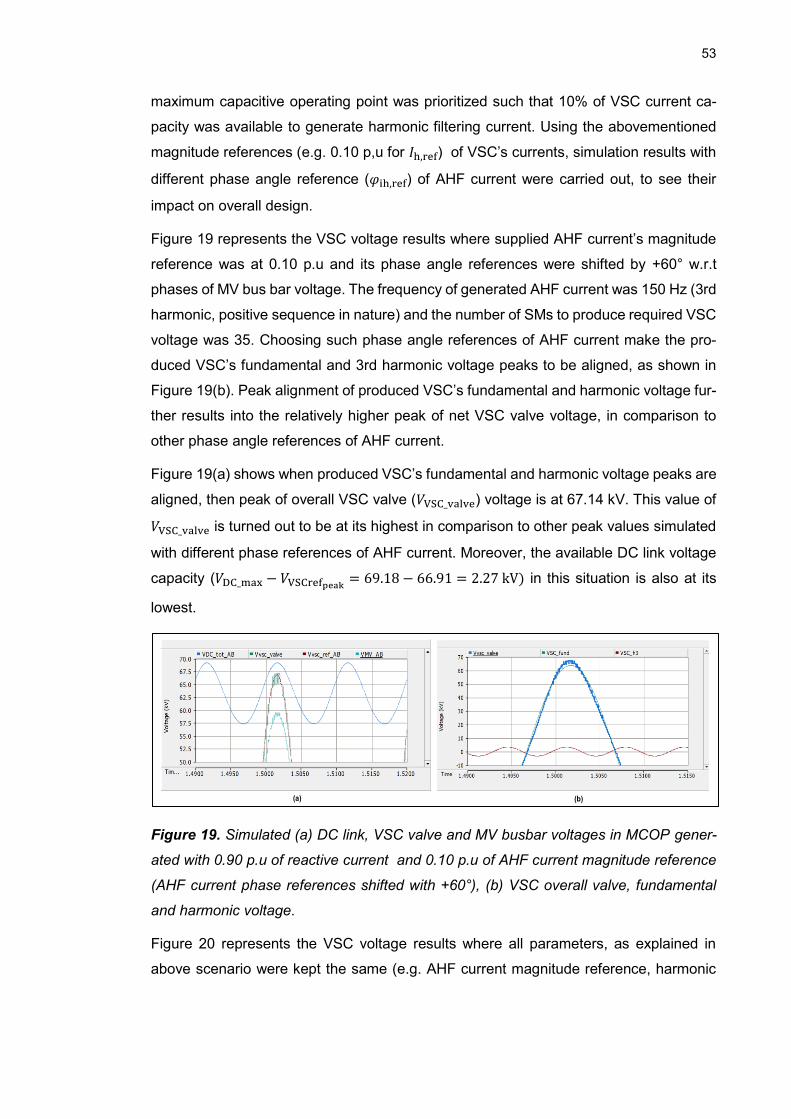
53
maximum capacitive operating point was prioritized such that 10% of VSC current ca-
pacity was available to generate harmonic filtering current. Using the abovementioned
magnitude references (e.g. 0.10 p,u for 𝐼h,ref) of VSC’s currents, simulation results with
different phase angle reference (𝜑ih,ref) of AHF current were carried out, to see their
impact on overall design.
Figure 19 represents the VSC voltage results where supplied AHF current’s magnitude
reference was at 0.10 p.u and its phase angle references were shifted by +60° w.r.t
phases of MV bus bar voltage. The frequency of generated AHF current was 150 Hz (3rd
harmonic, positive sequence in nature) and the number of SMs to produce required VSC
voltage was 35. Choosing such phase angle references of AHF current make the pro-
duced VSC’s fundamental and 3rd harmonic voltage peaks to be aligned, as shown in
Figure 19(b). Peak alignment of produced VSC’s fundamental and harmonic voltage fur-
ther results into the relatively higher peak of net VSC valve voltage, in comparison to
other phase angle references of AHF current.
Figure 19(a) shows when produced VSC’s fundamental and harmonic voltage peaks are
aligned, then peak of overall VSC valve (𝑉VSC_valve) voltage is at 67.14 kV. This value of
𝑉VSC_valve is turned out to be at its highest in comparison to other peak values simulated
with different phase references of AHF current. Moreover, the available DC link voltage
capacity (𝑉DC_max − 𝑉VSCrefpeak= 69.18 − 66.91 = 2.27 kV) in this situation is also at its
lowest.
Figure 19. Simulated (a) DC link, VSC valve and MV busbar voltages in MCOP gener-
ated with 0.90 p.u of reactive current and 0.10 p.u of AHF current magnitude reference
(AHF current phase references shifted with +60°), (b) VSC overall valve, fundamental
and harmonic voltage.
Figure 20 represents the VSC voltage results where all parameters, as explained in
above scenario were kept the same (e.g. AHF current magnitude reference, harmonic
(a) (b)

54
type, number of SMs, etc.) except the phase angle references. Here, phase angle refer-
ences of AHF current were shifted by +240° w.r.t phases of MV bus bar voltage. Choos-
ing such phase angle references of AHF current makes the produced VSC’s fundamental
and 3rd harmonic voltage peaks to be opposite to each other, as shown in Figure 20(b).
Since peaks of these voltages are in opposite direction, therefore, the peak of overall
VSC valve voltage also got decreased significantly in comparison to its value in Figure
20(b).
Figure 20. Simulated (a) DC link, VSC valve and MV busbar voltages in MCOP gener-
ated with 0.90 p.u of reactive current and 0.10 p.u of AHF current magnitude reference
(AHF current phase references shifted with +240°), (b) VSC overall valve, fundamental
and harmonic voltage.
Figure 20(a) shows when produced VSC’s fundamental and harmonic voltage peaks are
in the opposite direction, then the peak of overall VSC valve (𝑉VSC_valve) voltage is at
62.05 kV. Lower 𝑉VSC_valve peak also result into increasing the available DC link voltage
capacity (𝑉DC_max − 𝑉VSCrefpeak= 67.93 − 60.88 = 7.05 kV) which supposedly can be uti-
lised to decrease the number of required SMs from 35 to 34.
Consequently, the phase angle of AHF current affects the effective STATCOM design in
a way that if peaks of produced VSC’s fundamental and harmonic voltages are aligned,
then higher number of SMs is required, in comparison to the situation when peaks are
not aligned. But if peaks are opposite to each other, then there is a probability at least
with low order harmonic filtering current that less SMs might be needed to produce the
same VSC voltage. Moreover, because needed AHF current phase varies depending on
operating point and is not known in design phase, the worst-case approach needs to be
taken to be able to operate in all operating points.
(a) (b)

55
4.3.3 AHF current’s magnitude and frequency impact on design
In this section, the impact of different magnitudes and frequencies of AHF current on
STATCOM design has been investigated. The reactive current has been prioritised first,
and thereafter remaining current capacity was allocated to AHF current. For instance,
80% of VSC current was utilised to generate fundamental reactive current and rest for
AHF current generation. Speaking of frequencies, 3rd, 4th and 5th harmonics (150, 200
and 250 Hz) have been chosen to work out in this section. The phasor rotation of these
harmonics has been assumed to be positive sequence in all simulations. Only the num-
ber of SMs, reactive current’s magnitude reference, AHF current’s magnitude, frequency
and phase angle references were changed in the simulations, else other system param-
eters remained the same as defined earlier in chapter 4.3. All simulation results have
been worked out in the maximum capacitive operating point (MCOP).
Initially, simulation results with AHF current of 3rd order harmonic have been carried out.
The magnitude references were chosen such that after prioritising the fundamental re-
active current, remaining capacity for AHF current magnitude reference were sought to
be 20%, 40% and 60% of overall VSC current capacity. Thereafter, using the same set
of AHF current magnitude reference, simulation results with 4th, 5th and combined
(3rd+4th+5th) order of harmonics were worked out. Both worst (peak aligned) and best
(peak opposite) phase angle references, as defined in chapter 4.3.2, were used with
aforesaid simulation results.
Figure 21 represents the case where after prioritising fundamental reactive current, 20%
of current capacity was available to produce 3rd order positive sequence AHF current.
The phase angle references of 3rd order AHF current for worst peak situation, as ex-
plained in chapter 4.3.2, were sought to be shifted by +60° w.r.t phases of MV bus bar
voltage. The number of SMs used in this situation is 34 analogous to the situation when
full current capacity was used to generate only fundamental reactive current in MCOP
region (basic case design).
Figure 21(a) shows the waveforms of VSC’s voltages when simulated with aforesaid
AHF current’s magnitude, frequency and phase angle references. Here, it can be clearly
seen that peak value of VSC reference voltage (𝑉VSCrefpeak= 73.93 kV) is higher than
maximum of DC link voltage (𝑉DC_max = 67.80 kV). it signifies that available DC-link volt-
age is not enough to produce the desired valve voltage and thus the overall VSC current.
Further this DC link voltage was produced with 34 SMs and if same is not enough then
there is clearly a requirement to increase the number of SMs.

56
Figure 21. Simulated (a) DC link, VSC valve and MV busbar voltages in MCOP region
and 3rd order AHF current with 0.20 p.u of magnitude, worst peak phase angle (+60°)
and 34 submodules, (b) VSC phase current in delta winding.
Thereafter, simulations with the same AHF current references but with the increased
number (e.g. 35, 36) of SMs were repeated until enough DC link voltage is achieved.
Figure 23 shows the waveforms of VSC’s voltages and current with 37 SMs. In Figure
23(a), values of 𝑉VSCrefpeak and 𝑉DC_max are 69.94 kV and 73.35 kV respectively. It shows
that now there is 3.41 of remaining capacity in DC link voltage and therefore required
VSC voltage can be produced without violating the safety margin. Further, the RMS value
of MV bus bar voltage is 23.64 kV which is lower than the insulation voltage limit of 72.5
kV as defined in chapter 4.1.
Figure 23(b) represents the VSC’s current waveform. Here it can be clearly seen that
peak of VSC current stays below 2.1 kA. It’s net RMS value (𝐼vsc_rms) in delta winding
(i.e. AB phase) was 0.9960 kA wherein RMS value of fundamental current component
was at 0.9758 kA and 3rd order AHF current component was at 0.1996 kA. So, consid-
ering all system limitation required number of SMs to produce such an AHF current was
37.
Figure 22. Simulated (a) DC link, VSC valve and MV busbar voltages in MCOP region
and 3rd order AHF current with 0.20 p.u of magnitude, worst peak phase angle (+60°)
and 37 submodules, (b) VSC phase current in delta winding.
(a) (b)
(a) (b)

57
Hence, prioritising fundamental reactive current such that 20% of overall VSC current is
used for 3rd order AHF current, result into increasing the number of SMs by 3, in com-
parison to the situation where entire current capacity was used only for the fundamental
reactive current only (basic design case in MCOP).
Now simulations were carried out assuming 40% of current capacity was available to
produce 3rd order positive sequence AHF current, with its worst-case phase angle. Start-
ing with 37 SMs, same situation happened as described in Figure 21, where DC link
voltage capacity was not enough to produce the required VSC voltage. Therefore, the
number of SMs was increased until all system limitations were satisfied.
The needed number of SMs to produce 0.40 p.u of AHF current was worked out to be
39, and to validate the same simulated VSC’s voltage and current results are shown in
Figure 23. Here, Figure 23(a) shows the values of 𝑉VSCrefpeak and 𝑉DC_max as 75.82 kV
and 77.87 kV respectively and signify the remaining DC link voltage capacity of 2.05 kV.
The RMS value of MV bus bar voltage was at 23.57 kV. Figure 23(b) depicts that 𝐼vsc_peak
is much below than 2.1 kA and value of 𝐼vsc_rms in delta winding was at 0.9991 kA wherein
RMS value of fundamental current component was at 0.9167 kA and 3rd order AHF
current component was at 0.3973 kA. Thus 39 is the adequate number of SMs to produce
such AHF current without violating any of the system limitations.
Figure 23. Simulated (a) DC link, VSC valve and MV busbar voltages in MCOP region
and 3rd order AHF current with 0.40 p.u of magnitude, worst peak phase angle (+60°)
and 39 submodules, (b) VSC phase current in delta winding.
Prioritising fundamental reactive current such that 40% of overall VSC current capacity
is used for 3rd order AHF current, results into increasing the number of SMs from 34 to
39, in comparison to the basic design case in MCOP region with fundamental reactive
current only.
Next simulation was carried out, assuming 60% of current capacity was available to pro-
duce 3rd order positive sequence AHF current, with its worst-case phase angle. The
(a) (b)

58
needed number of SMs to produce 0.60 p.u of AHF current, with an iterative process of
enough DC link capacity, sought out to be 42. Figure 24 depicts the VSC’s voltage and
current results when simulated with 42 SMs for 0.60 p.u of AHF current in the MCOP
region.
Figure 24(a) shows that with 42 SMs there is enough DC link capacity (VDC_max −
𝑉VSCrefpeak= 84.18 − 81.24 = 2.94 kV) after producing the desired VSC voltage and so
thus the current. The RMS value of MV bus bar voltage was at 23.49 kV. Figure 24(b)
depicts that 𝐼vsc_peak is lower than 2.1 kA and value of 𝐼vsc_rms in delta winding was at
0.9999 kA wherein RMS value of fundamental current component was at 0.7999 kA and
3rd order AHF current component was at 0.5997 kA. Hence, prioritising fundamental
reactive current such that 60% of overall VSC current capacity is used for 3rd order AHF
current, result into increasing the number of SMs from 34 to 42, in comparison to the
basic design case in MCOP region with fundamental reactive current only.
Figure 24. Simulated (a) DC link, VSC valve and MV busbar voltages in MCOP region
and 3rd order AHF current with 0.60 p.u of magnitude, worst peak phase angle (+60°)
and 42 submodules, (b) VSC phase current in delta winding.
To check how phase angle reference impacts the number of SMs with 3rd order har-
monic, case of 0.40 p.u AHF current was re-simulated. But this time instead of using the
worst peak phase angle references (+60° phase shift), best peak phase angle references
(+240° phase shift) for AHF current were used. Figure 25(a) shows there is enough re-
maining DC link capacity (𝑉DC_max − 𝑉VSCrefpeak= 74.00 − 60.68 = 13.32 kV) in phase AB
and therefore the number of SMs can be reduced from 39 to an adequate value. But this
DC link capacity is not equally available in all of the VSC’s phases. Figure 25(b) shows
the waveform of VSC voltages in phase BC with 39 SMs. Here, the remaining DC link
capacity (𝑉DC_max − 𝑉VSCrefpeak= 77.82 − 74.72 = 3.01 kV) after producing the desired
valve voltage is close to the system limit defined in chapter 4.1. And decreasing SMs
further would result in violation of system limitation of safety margin in DC link voltage
(a) (b)

59
capacity of BC phase. So from these two results, it can be implied that choosing best
peak phase angle may free some DC link capacity in one phase, but it’s not necessary
that same capacity will be available in other phase too.
Figure 25. Simulated DC link, VSC valve and MV busbar voltages in MCOP region and
3rd order AHF current with 0.40 p.u of magnitude, best peak phase angle (+240°) and
39 submodules (a) phase AB (b) phase BC
So far, cases with 3rd order AHF current were simulated and its different magnitudes
and phase angles impact on the needed number of SMs have been investigated. Having
said that, instead of 3rd order, now all of these simulations should be repeated with 4th
order, 5th order and combined order (3th, 4th and 5th) of AHF currents with the same
approach of choosing 0.20, 0.40 and 0.40 p.u of magnitude references along with their
respective worst phase angle references in MCOP region. However, since the method
of analysing impact of these AHF currents remain the same (e.g. validating remaining
DC link capacity, rms value of MV busbar voltage and VSC current limit in delta winding).
Therefore, all the simulation results with these AHF currents were segregated and shown
in Table 7.
Starting with 4th order AHF current, its worst and best peak conditions occured when its
phase angle references are shifted by +20° and +200° w.r.t phases of MV bus bar volt-
age. As shown in Table 7, with worst peak angle reference in MCOP region, the needed
number of SMs to produce 0.20, 0.40 and 0.60 p.u of 4th order AHF current (along with
prioritised reactive current), after complying with all system limitations, sought out to be
39, 43 and 47 respectively. Thereafter, using the same approach, simulation for 5th order
AHF current were carried out and its worst and best peak conditions found out to be
shifted by +0° and +180° w.r.t phases of MV bus bar voltage. And, to produce the same
set of magnitudes (as mentioned above) for this order of AHF current, the needed num-
ber of SMs turned out to be 40, 46 and 50 respectively.
In last, impact of combined AHF currents of different frequencies, different magnitude
and phase angle references on the needed number of SMs were also investigated. The
(a) (b)

60
frequency reference for these AHF currents were 150, 200 and 250 Hz (3rd, 4th and 5th
order). Though each of the AHF currents was provided with its own magnitude reference
but magnitude reference of net AHF current (computed through equation 4.2 mentioned
in chapter 4.1) was chosen to be 20%, 40% and 60% of overall VSC’s current capacity.
Moreover, worst-peak phase angle references of each harmonic current were consid-
ered, such as 60° (phase shift w.r.t MV busbar voltage) for 3rd harmonic, 20° for 4th
harmonic and 0° for 5th harmonic filtering current.
Thus, simulation results with combined 3rd, 4th and 5th order AHF currents are shown
in Table 7. From these results it can be concluded that producing AHF current with mag-
nitudes of 0.20, 0.40 and 0.60 p.u result into the highest number of SMs as 42, 50 and
55 respectively, in comparison to the same magnitude of AHF current comprising only
single harmonic.
Table 7. Simulation results with different magnitude and phase angle of AHF current comprising 4th, 5th and combined order of harmonics
4.3.4 Negative sequence AHF current impact on design
In practical application, harmonics present in the network might be of any phasor rotation.
Therefore, AHF current to compensate those harmonics would also be of any phasor
rotation (e.g. positive, negative or zero sequence). Since studied STATCOM is a delta
arrangement of three phase MMC branches, therefore it can not be utilised to produce
zero sequence AHF current. But it certainly can produce positive and negative sequence
AHF current.
In the previous chapter, simulations were carried out with positive sequence AHF current
of different magnitudes and frequencies. But, in this chapter, simulation results showing
impact of negative sequence AHF current have been worked out. Speaking of frequency,
simulations were worked out with 5th order AHF current, since 5th harmonic is negative
sequence in nature if supplying network is balanced. Hence, after prioritising fundamen-
tal reactive current, the available current capacity of the AHF current was assumed to be

61
20% of overall VSC current. The phase angle references of AHF current were chosen to
be negative sequence in worst peak condition (0° phase shift w.r.t MV busbar voltage).
Figure 26 represents the simulated VSC’s voltage and current waveforms with negative
sequence AHF current.
The needed number of SMs to produce desired AHF current magnitude with enough
remaining DC link capacity sought to be 40, through multiple iteration. As shown in Figure
26(a), the remaining DC link capacity in this case is at 2.70 kV (𝑉DC_max − 𝑉VSCrefpeak=
78.28 − 75.58). Comparing this value with remaining DC link capacity of the same mag-
nitude but positive sequence 5th order AHF current, shown in Table 7, it turned out that
same was 2.72 kV earlier. Hence no significant difference in available DC link voltage,
and therefore the number of SMs in both cases also remain the same.
Figure 26. Simulated (a) DC link, VSC valve and MV busbar voltages in MCOP region
and 5th order AHF current with 0.20 p.u of magnitude, negative phase sequence in worst
peak phase angle (0°) and 40 submodules, (b) VSC phase current in delta winding.
Comparing VSC current results, in Figure 26(b) and Table 7 value of 𝐼vsc_peak remains
unchanged at 1.67 kA, irrespective to the condition whether AHF current is positive or
negative sequence in nature. Here, RMS value of VSC’s fundamental current component
in positive sequence case was 0.9686 kA and 0.9689 kA in negative sequence case.
The value of zero sequence current in both of the cases was not significantly high; 3.28
and 3.14 A respectively.
Hence, the above mentioned simulation results suggest that changing phasor rotation of
AHF current from positive to negative sequence doesn’t affect much the overall STAT-
COM design. Because, the number of needed SMs to produce desired VSC voltage and
other system parameters (e.g. DC link capacity, VSC current peak value) almost remain
unchanged. Nevertheless, cases of 0.40 and 0.60 p.u magnitude references with nega-
tive sequence AHF current were simulated. Later these results have been compared with
the results of positive sequence AHF current of the same magnitude. Table 8 represents
(a) (b)

62
the data of available DC-link voltage and the needed number of SMs to produce a certain
magnitude of AHF current with both positive and negative sequence in nature. Here it
can be clearly seen that the value of needed SMs (e.g. 40) does not deviate whether its
0.20 p.u AHF current of positive sequence or negative sequence.
Table 8. Comparison of Number of SMs and available DC-link voltage with 5th order
positive and negative sequence AHF current.
4.3.5 Coupling inductor and transformer reactance impact on design
In this chapter, the impact of coupling inductor’s and transformer’s reactance has been
investigated. One of the main functions of the coupling inductor is to restrict the amount
of harmonic current drawn from the grid due to presences of harmonics in VSC’s output
voltage. Moreover, VSC’s net impedance seen from the grid side is the summation of
coupling inductor and transformer’s reactance. Higher the value of this impedance is,
better the harmonic attenuation would be. But increasing the reactance value of the cou-
pling inductor comes with two possible consequences. First, large inductor value makes
the system dynamic slower. Second, as per the equation 3.7 mentioned in chapter 3.3.1,
to produce a fixed amount of capacitive reactive current, more VSC voltage is needed
with higher reactance value.
To produce higher VSC voltage, more SMs are needed which ultimately affects its de-
sign. Hence, to show the effect of how increasing or decreasing the reactance value
affects the needed number of SMs, two cases for each coupling inductor and transformer
reactance have been simulated. Thereafter, the results of these cases have been com-
pared with the pre-defined system values.
Starting with coupling reactance, its system value of 13 mH was chosen in all of the
simulations till now. But now, to check its effect on needed SMs, cases with 16 mH and
11 mH have been simulated. First simulation, with 16 mH of coupling reactance and
assuming 20% of current capacity was available to produce combine 3rd, 4th and 5th
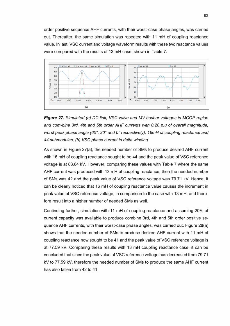
63
order positive sequence AHF currents, with their worst-case phase angles, was carried
out. Thereafter, the same simulation was repeated with 11 mH of coupling reactance
value. In last, VSC current and voltage waveform results with these two reactance values
were compared with the results of 13 mH case, shown in Table 7.
Figure 27. Simulated (a) DC link, VSC valve and MV busbar voltages in MCOP region
and com-bine 3rd, 4th and 5th order AHF currents with 0.20 p.u of overall magnitude,
worst peak phase angle (60°, 20° and 0° respectively), 16mH of coupling reactance and
44 submodules, (b) VSC phase current in delta winding.
As shown in Figure 27(a), the needed number of SMs to produce desired AHF current
with 16 mH of coupling reactance sought to be 44 and the peak value of VSC reference
voltage is at 83.64 kV. However, comparing these values with Table 7 where the same
AHF current was produced with 13 mH of coupling reactance, then the needed number
of SMs was 42 and the peak value of VSC reference voltage was 79.71 kV. Hence, it
can be clearly noticed that 16 mH of coupling reactance value causes the increment in
peak value of VSC reference voltage, in comparison to the case with 13 mH, and there-
fore result into a higher number of needed SMs as well.
Continuing further, simulation with 11 mH of coupling reactance and assuming 20% of
current capacity was available to produce combine 3rd, 4th and 5th order positive se-
quence AHF currents, with their worst-case phase angles, was carried out. Figure 28(a)
shows that the needed number of SMs to produce desired AHF current with 11 mH of
coupling reactance now sought to be 41 and the peak value of VSC reference voltage is
at 77.59 kV. Comparing these results with 13 mH coupling reactance case, it can be
concluded that since the peak value of VSC reference voltage has decreased from 79.71
kV to 77.59 kV, therefore the needed number of SMs to produce the same AHF current
has also fallen from 42 to 41.
(a) (b)

64
Figure 28. Simulated (a) DC link, VSC valve and MV busbar voltages in MCOP region
and com-bine 3rd, 4th and 5th order AHF currents with 0.20 p.u of overall magnitude,
worst peak phase angle (60°, 20° and 0° respectively), 11mH of coupling reactance and
41 submodules, (b) VSC phase current in delta winding.
Transformer reactance is the other crucial passive element of VSC which affects the
number of needed SMs to produce the desired voltage. Its system value of 0.10 p.u was
chosen in all of the simulations until now. But now to check its effect, cases with 0.15 p.u
and 0.05 p.u of transformer reactance with 20% available capacity (post RPC prioritisa-
tion) for AHF current generation was carried out. Here, combined 3rd, 4th and 5th order
of harmonic filtering current, positive sequence in nature and having worst-case phase
angle reference, has been used. VSC current and voltage waveform results with these
two reactance values were compared with the results of 0.10 p.u transformer reactance
case of the same AHF current shown in Table 7.
Figure 29(a) depicts that the needed number of SMs to produce desired AHF current
with 0.15 p.u of transformer reactance sought to be 45 and peak value of VSC reference
voltage is at 86.31 kV. Comparing these values with Table 7 wherein the same AHF
current was produced with 0.10 p.u of transformer reactance, then the needed number
of SMs was 42 and the peak value of VSC reference voltage was 79.71 kV.
Figure 29. Simulated (a) DC link, VSC valve and MV busbar voltages in MCOP region
and com-bine 3rd, 4th and 5th order AHF currents with 0.20 p.u of overall magnitude,
worst peak phase angle (60°, 20° and 0° respectively), 0.15 p.u of transformer reactance
and 45 submodules, (b) VSC phase current in delta winding.
(a) (b)
(a) (b)

65
In last, the value of transformer reactance was decreased to 0.05 p.u and simulation to
produce the same AHF current (as did last case) was carried out. Here, now the needed
number of SMs to produce desired AHF current sought to be 38 and the peak value of
VSC reference voltage is at 73.03 kV, shown in Figure 30(a). Comparing these values
with Table 7 where the same AHF current was produced with 0.10 of transformer reac-
tance, the values of these parameters were 42 and 79.71 kV respectively.
Therefore, it can be concluded that increasing the transformer reactance value from 0.10
to 0.15 p.u result in increment in peak value of VSC voltage reference from 79.71 to
86.31 kV and consequently increment into the needed number of SMs from 42 to 45 as
well. Similarly, decreasing the same reactance value from 0.10 to 0.05 p.u result into
decrement in peak value of VSC voltage reference from 79.71 to 73.03 kV and conse-
quently decrement in the needed number of SMs from 42 to 38 as well.
Figure 30. Simulated (a) DC link, VSC valve and MV busbar voltages in MCOP region
and com-bine 3rd, 4th and 5th order AHF currents with 0.20 p.u of overall magnitude,
worst peak phase angle (60°, 20° and 0° respectively), 0.05 p.u of transformer reactance
and 38 submodules, (b) VSC phase current in delta winding.
4.3.6 Summary of case 1
In chapter 4.3, it was investigated that how combined operation of RPC and AHF of
studied STATCOM affects its design. Here, combined operation was such that RPC was
prioritised over the AHF operation. After reconciling all simulation results, as shown in
Appendix B, Table 1, it was found out that additional AHF operation affects the STAT-
COM design, so thus the needed number of SMs, in three ways. First was the magnitude
of AHF current. It can be clearly seen in the aforementioned table that when magnitude
of an AHF current goes high (e.g. 20%, 40%), then an increment in the needed number
of SMs w.r.t basic design was noticed.
Second was the phase angle references of AHF current. Here, if phase angle references
of AHF current and chosen such that the peaks of produced VSC’s fundamental and
(a) (b)

66
harmonic voltages are aligned, then the peak of resultant VSC voltage may go even
more higher, in comparison to the situation when peaks are not aligned. The higher peak
of resultant VSC voltage means the requirement of higher DC link voltage and thus more
SMs. But if peaks are opposite to each other, fewer SMs are required to produce the
same VSC voltage. And, because AHF current angle changes according to the operating
point, worst case angle should be considered in design to be able to operate in all oper-
ating points.
The third effect on STATCOM design was based on the order of AHF current produced.
As shown Appendix B, Table 1, the number of needed SMs to produce an AHF current
of 5th order was higher than the same magnitude AHF current of 3rd order, for instance,
case of 20% of overall STATCOM current capacity. Also, when combining three harmon-
ics, with same total RMS current magnitude, the needed number of submodules was
higher than with any of the single harmonic only. This seems to be due to reason that
harmonic currents cancel each other part of the cycle (reducing current RMS) but they
increase the total VSC voltage peak. Further, simulations to produce the same magni-
tude of AHF current but with negative sequence of phasor rotation were also worked out.
And, no significant impact on STATCOM design was noticed, in comparison to all posi-
tive sequence based AHF current scenarios. Additionally, the impact of transformer and
coupling inductor ‘s reactance was investigated. Increasing reactance value for both of
these components resulted in an increase in the needed number of SMs to produce the
same amount of current.
In summary, since the number of submodules is increased significantly in some cases
due to AHF, it increases costs considerably. In order to benefit from AHF without over-
dimensioning the STATCOM, it can also be done so that the number of submodules is
kept same as in RPC mode only (e.g. 34 SMs). And, then the AHF current will be limited
by control so that we will not end up into higher VSC voltage stress than in RPC mode
only. This way AHF can still be utilized well in many operating points but in extreme
cases its use is more limited.
4.4 Case 2: Full RPC support in parallel to AHF operation
In this chapter, the design of STATCOM when it is required to produce nominal funda-
mental current/power and perform active harmonic filtering at the same time has been
carried out. For example, produce 100 MVAr reactive power and decrease 5th and 7th
harmonic voltages at PCC from 2 % to 1 % simultaneously. Speaking of priority, zero
sequence circulating current and active fundamental frequency current are prioritized
first but then reactive current and active harmonic filtering have the same priority. Here,

67
it was of main interest to investigate how to design STATCOM effectively (without signif-
icant over dimensioning) so that both requirements are satisfied.
As part of the design process, first needed VSC harmonic current to filter out harmonic
voltage at the PCC has been calculated. Here, while computing needed AHF current,
how network impedance affects its magnitude value has also been explained. Thereaf-
ter, using the nominal value of fundamental reactive current and computed AHF current,
total current at the PCC was worked out. Using this value and HV side PCC voltage, the
net MVAr capacity of STATCOM was defined. MV bus bar voltage was calculated as per
the system limitation of maximum phase current in delta winding and voltage insulation
level defined in chapter 4.1. Next, values of coupling inductor and transformer reactance
were calculated iteratively, as per the MVAr capacity. In last, the number of needed sub-
modules to generate such a combine RPC and AHF current was investigated by the
simulations.
To find out the needed number of SMs, all possible worst-case situation (highest needed
VSC voltage), as worked out in chapter in 4.3, were considered. First, worst situation can
be defined when network voltage is at its maximum continuous value, STATCOM pro-
ducing the reactive and AHF current in MCOP region and fundamental and harmonic
VSC voltage peaks occurring at the same time. Second, worst situation occurs when
entire STATCOM capacity is used to produce reactive current (no AHF current) in the
MIOP region during a short time overvoltage condition.
Considering above mentioned worst cases, an effective STATCOM design was carried
out and, then the same was tested with unbalance supply network. The main motive to
test STATCOM design with an unbalance supply was to see the effect of zero sequence
current on the needed number of SMs and effect on needed MV busbar voltages to pro-
duce the required reactive and AHF currents. Further, it was also of interest to check
whether any worst-case situation with voltage unbalance also exists.
Parameters of simulation model almost remain the same, except STATCOM MVAr rat-
ing, secondary side nominal L-L RMS voltage and inductance of coupling coil. These
parameters have been recalculated in chapter 4.4.2, hence mentioned accordingly. In-
formation on the number of submodules used per branch was retrieved after simulating
the worst-case scenarios as mentioned in chapter 4.4.2. Finally, detailed information on
the network and STATCOM parameter have been enclosed in Appendix A, Table 2.

68
4.4.1 Calculating needed harmonic current for AHF
Characteristics of frequency-dependent system impedance at PCC affects the STAT-
COM design and its rating. Changing impedance of transmission line, passive compo-
nents (e.g. capacitors, inductors) and voltage control devices available in the vicinity and
changing dynamics of loads are among those affecting factors. Further, information on
harmonic emission caused by STATCOM, phase angles, magnitude and level of back-
ground harmonics, any other harmonic source in the vicinity and permissible harmonic
distortion limit at the PCC are other aspects for a STATCOM design. [57]
Hence, considering the objectives of this thesis, the harmonic compensation perfor-
mance of studied STATCOM has not been evaluated in this work. Because, the main
goal of this thesis is to check whether studied STATCOM can produce a certain harmonic
filtering current of a different order and phase sequences, combined with the fundamen-
tal reactive current. Therefore, background harmonic source, other harmonic filtering de-
vices, any capacitor, inductor, other voltage control devices and system loads have not
been considered in the simulation except the transmission line impedance.
Since transmission line impedance is a frequency-dependent function, therefore its value
changes with different harmonic orders. To compensate certain voltage distortion, infor-
mation on needed harmonic filtering current is needed. This harmonic filtering current
then further depends on system harmonic impendence and can be computed with the
following equation.
𝐼h =𝑉ℎ
𝑍h (4.6)
Where, 𝑉h is the RMS value of harmonic voltage, 𝑍h is transmission line harmonic im-
pedance in ohm and 𝐼h is the RMS value of filtering current produced by STATCOM to
mitigate the harmonic voltage, same is shown in Figure 31(a). Equation 4.6 shows that
the amount of needed filtering current is inversely proportional to the system impedance.
It means the higher filtering current is needed to compensate the same amount of voltage
distortion when system impedance is at its lowest, comparison to the situation when it is
high.

69
Figure 31. (a) Harmonic filtering and system impedance, (b) Impedance characteristics
at PCC [57].
Hence, transmission line impedance data considering different network conditions (e.g.
other available filtering devices) should be measured. But if impedance measurements
are not available, then its value can be assumed to be any magnitude within the circle
shown, as shown in Figure 31(b). This circle represents the information on impedance
data where the y-axis denotes the reactance and the x-axis denotes the resistance of a
transmission line. Typically value of maximum possible impedance magnitude (shown
by R2) varies from 100-200 ohms with impedance angle in the range of 75-80 degrees
respectively. In last, R1 represents the minimum network impedance can be of any mini-
mum value possible. [57]
Subsequently, since no transmission line impedance data was available for this work,
therefore, STATCOM design has been carried out while assuming the minimum value of
system impedance, as suggested in Figure 31(b). Because, choosing lower system im-
pedance would result in higher harmonic filtering current requirement, and thus one of
the worst conditions a network can offer.
Therefore, using network data mentioned in Appendix A, Table 2, a case of 2% voltage
distortion at PCC (primary side voltage of 220 kV) was assumed. Here, voltage distortion
was decided to be mitigated to 1% with minimum transmission line harmonic impedance
of 22 ohms (an arbitrary value), at 150 Hz of frequency or in other words, 3rd harmonic.
Consequently, the maximum needed filtering current from the STATCOM to perform
such compensation will be as followed.
𝐼h =𝑉h(max)
𝑍h(min)=
(2% ∗ 220 kV − 1% ∗ 220 kV)
22 ohms=
2.2
22= 100 A
Hence, 100 A of needed primary side AHF current has been worked out to dimension a
STATCOM for mitigating voltage harmonic distortion from 2% to 1% at PCC, with 22
ohms of minimum harmonic impedance.
system harmonic impedance Zh
Harmonicfiltering current source
(STATCOM)
PCC
Vh
Ih(filtering)
Grid source
(a) (b)

70
4.4.2 Dimensioning STATCOM parameters
Earlier 100 MVAr rated STATCOM was producing 1000 A of current in MCOP region
with its maximum current capacity. This current was prioritised in a way that entire current
capacity was used for reactive power when needed and when all was not needed the
remaining capacity was used to produce the AHF current. However, now, a STATCOM
has been designed which should produce 100 MVAr of reactive power and thereafter
some more capacity should be added in a way that it can produce the 100 A of AHF
current too, as computed in chapter 4.4.1. Hence, it was of interest to rate the STAT-
COM’s MVAr with such parallel RPC and AHF operation.
The primary side fundamental reactive current (RMS) of a 100 MVAr STATCOM, con-
nected to PCC through a 220/34.1 kV step down transformer (in YNd11 connection), can
be calculated as follows.
𝐼fund_reactive =𝑄STATCOM
(√3∗VLL_primary) (4.7)
𝐼fund_reactive =100 MVAr
(√3 ∗ 220 kV)= 262.43 A
The above-mentioned current is the maximum amount of reactive current present on the
primary side of PCC to regulate its voltage. However, to compensate voltage distortion
at PCC from 2% to 1%, the needed value of maximum filtering current (due to minimum
harmonic impedance) on the primary side is 100 A. Hence, on the primary side of PCC
now there will be two current components as fundamental reactive current and active
harmonic filtering current.
From equation 4.2, total RMS value of fundamental and AHF current to be produced by
a STATCOM can be calculated as mentioned below.
𝐼PCC_primary = √𝐼fund_reactive2 + 𝐼h,max
2 = √262.432 + 1002 = 280.83 A (4.8)
The earlier STATCOM was only rated to produce 262.43 A of reactive current on the
primary side of its transformer. Hence, in order to produce a combine AHF and reactive
current of 280.83 A of magnitude, the MVAr capacity of STATCOM should be revised as
mentioned below.
𝑄STATCOM,revised = 𝐼PCC_primary ∗ √3 ∗ 𝑉LL_primary (4.9)
𝑄STATCOM,revised = 280.83 A ∗ √3 ∗ 220 kV = 107 Mvar
After calculating the needed MVAr of STATCOM and primary side PCC current, next
was to check whether secondary side current remain below the maximum RMS current

71
limit of STATCOM. In delta winding maximum RMS current limit of studied STATCOM
(VSC) was 1000 A or 1732.05 (√3*1000) in wye-winding (secondary side of PCC).
Since transformer was rated with 220/34.1 kV, its secondary side current would be as
follows.
𝐼PCC_secondary =𝑄STATCOM,revised
(√3∗VLL_secondary) (4.10)
𝐼PCC_secondary =107 MVAr
(√3 ∗ 34.1 kV)= 1811.62 A = IVSC_wye
The value of secondary side current calculated through equation 4.10 certainly exceeds
the limit of wye-winding current of VSC (𝐼VSC_wye). To restrict this value, there were two
options either to decrease the MVAr of STATCOM or increase the line to line secondary
side voltage of the transformer. MVAr can not be decreased, since it has been calculated
according to the needed fundamental reactive and AHF current. Therefore, increasing
the value of secondary side voltage was decided. The value of 1730.43 A secondary
current or wye-winding VSC current (close to the defined limit) was chosen and accord-
ingly, adequate secondary side voltage was worked out to be 35.7 kV.
𝐼PCC_secondary(revised) =107 MVAr
(√3∗35.7 kV)= 1730.43 A or 1.730 kA = IVSC_wye (4.11)
Since MVAr of STATCOM and value of secondary side voltage have been revised, there-
fore the earlier value of coupling reactor (e.g. 13 mH) and the needed number of SMs
(e.g. 34) were also no longer valid and needed to be re-calculated using the equation
mentioned below (4.12) and simulator.
A fault happening on the secondary busbar results into the flow of a fault current from
VSC to the secondary busbar. This current is then limited by the coupling inductor and if
capacity has been increased and so thus the DC link voltage, then reactance value of
coupling inductor should also be increased directly proportional to the increase of num-
ber of submodules. Hence, it was decided that to compute the adequate reactance of
coupling inductor, an iterative approach should be adopted while linking information com-
ing from both platforms (equation 4.12 and simulator). As a part of the iteration, first 13
mH of reactance value was used and the needed number of SMs was retrieved through
simulation. Thereafter, new reactance was computed after rationalising the value of
needed SMs coming from the simulator, initial reactance of 13 mH and needed SMs
suggested by the equation 4.12, example given below.
Inductance in the original 100 MVAr design
SMs in the original 100 MVAr design=
X mH
SMs computed with simulation (4.12)

72
13 mH
38=
X mH
46
Now, newly computed reactance value was supplied to the simulator to validate whether
the recommended number of SMs from the last iteration comply with the new reactance
value or there was a change in it. Because, if there was an increment in the number of
needed SMs for the simulator, then again new value of reactance was computed through
equation 4.12 and this iterative process was continued until there was no increment in
the number of SMs.
Hence, simulation to produce desired positive sequence AHF current of 3rd order (or
150 Hz of frequency) along with fundamental reactive current were carried out. And, after
three iterations, final reactance value of coupling inductor and the needed number of
SMs worked out to be were 15.73 mH and 41 SMs respectively, in accordance with both
equation 4.12 and simulation-based limitations. The value of transformer reactance has
been kept the same as 0.10 p.u. Hence, all STATCOM related parameters to produce
280.83 A of combined fundamental reactive current and AHF current have been dimen-
sioned. Now next was to simulate a sample case with these values to check whether
system limitations mentioned in chapter 4.1 have been fulfilled or not.
Figure 32 represents the simulation results carried out to produce 280.83 A of VSC
(STATCOM) current on the primary side of PCC. This current should comprise of 262.43
A (RMS) of fundamental reactive current and 100 A of AHF current on the primary side
of PCC. The phase angle references of AHF current was chosen to be 60° phase shifted
w.r.t MV busbar voltage (worst peak angle reference). Here, secondary side PCC current
or VSC current in wye-winding should not exceed more than 1730.43 A (RMS), as cal-
culated through equation 4.1, and accordingly VSC current in delta winding should not
exceed 1000 A (RMS).
The needed number of SMs to produce the desired current at the primary side of PCC
with enough remaining DC link capacity sought to be 41. As shown in Figure 32(a), the
remaining DC link capacity in this case was at 3.02 kV (𝑉DC_max − 𝑉VSCrefpeak= 81.60 −
78.58). Moreover, MV busbar voltage was found to be 24.71 kV. Hence, all voltage-based
system limitations were satisfied.
However, there were some violations based on the defined current limits. Starting with
Figure 32(b), RMS value of primary side PCC current (𝐼PCC) in all phases was close to
280 A, depicted in Figure 32(d). Using FFT block function of PSCAD, values of funda-
mental current (𝐼PCC_fund) and AHF (𝐼PCC_filtering) current at the PCC were also validated
and turned out to be 262.84 and 99.79 A respectively. But, VSC current RMS value in

73
some of the phases of delta winding was founded to be more than 1000 A, shown in
Figure 32(b). Also, the maximum RMS value of VSC current in wye-winding (IVSC_Y), as
shown in Figure 32(c) was found to be 1737.51 A (A-phase) which is more than the
defined limit of 1730.43 A as computed in equation 4.11.
Figure 32. Simulated (a) DC link, VSC valve and MV busbar voltages in MCOP region
(with worst peak angle) to produce maximum AHF and fundamental reactive current at
PCC, simultaneously, (b) VSC phase current RMS values in delta-winding (c) VSC phase
current RMS values in wye-winding (d) Phase current RMS values at primary side of
PCC.
The simulation results shown in Figure 32 signify the violation of defined VSC current
limit in wye/delta winding. Here, one of the possible reasons behind such violation was
expected to be caused by the worst peak angle references of AHF current. Therefore, it
was of interest to check whether other phase angle reference of AHF current can help in
achieving the desired 280 A of combined current without violating wye or delta winding
VSC current limit. Hence, simulation with different phase angle references was carried
out and phase shift of 240° w.r.t busbar voltage (best peak angle case) turned out to be
the phase angle reference of the AHF current where combined current of 277.18 A at
the PCC was achieved, which was very close to the desired combined current of 280 A,
without violating any current or voltage limit.
Figure 33 shows the simulation result with the best peak angle reference (240° w.r.t
busbar voltage) of AHF current. Here, 41 SMs were needed to produce the desired cur-
rent with enough remaining DC link capacity as shown in Figure 33(a) (𝑉DC_max −
𝑉VSCrefpeak= 81.51 − 78.47 = 3.04 kV) and MV busbar voltage was at 24.68 kV. VSC cur-
rent RMS values in both wye and delta winding remained below their defined limits and
can be validated from Figure 33(b) and Figure 33(c). RMS value of primary side PCC
current (𝐼PCC) in all phases was slightly less than 280 A, depicted in Figure 33(d). Further,
RMS values of fundamental current and AHF current at the PCC were also validated and
turned out to be 260.01 and 99.72 A respectively.
(a)
(b) (c)
(d)
IPC...
Ipcc(A)_rms
280.697
IPC...
Ipcc(B)_rms
281.141
IPC...
Ipcc(C)_rms
279.812
VSC...
Ivsc_AB_r...
1001.38
VSC...
Ivsc_BC_rms
1001.23
VSC...
Ivsc_CA_r...
999.724
IVS...
IvscY(A)rms
1737.51
IVS...
IvscY(B)rms
1732.93
IVS...
IvscY(C)rms
1729.71

74
Figure 33. Simulated (a) DC link, VSC valve and MV busbar voltages in MCOP region
(with best peak angle) to produce maximum AHF and fundamental reactive current at
PCC, simultaneously, (b) VSC phase current RMS values in delta-winding (c) VSC phase
current RMS values in wye-winding (d) Phase current RMS values at primary side of
PCC.
Results shown in Figure 32 suggest that even after choosing an adequate secondary
side voltage of 35.7 kV and required MVAr of STATCOM, RMS value of 𝐼VSC_wye ex-
ceeded its defined limit due to certain phase angle of AHF current. Further, it explains
that the summation principle given in literature (equation 4.8) seems not to be enough to
quite satisfy the both maximum of fundamental reactive current and maximum of AHF
current requirements even though we are close to the requirements. Also, many worst-
case assumptions occurring at the same time (maximum needed harmonic voltage filter-
ing, minimum network impedance present, maximum reactive current needed) were also
considered.
Hence, it would be pertinent to say that, to see the design capability with this summation
principle, any of these currents’ magnitude should be decreased and this kind of small
deviation might be acceptable. But if not acceptable, then another option to avoid current
limitation violation is through higher MV busbar voltage (to restrict increasing PCC cur-
rent) which further results in requiring larger number of submodules and therefore in-
creased overall costs. Having said that, first an economical design utilising this geomet-
rical summation principle but slightly decreased value of AHF current to fulfil the system
limitation has been carried out. Thereafter, a conservative design in chapter 4.4.5, based
on an arithmetical summation principal and where both current requirements are easily
achieved, has been discussed.
Speaking of economical design, since reactive power compensation was assumed to be
a critical system requirement, the value of AHF current was decided to be decreased
from the target value of 100 A to a certain value until 𝐼VSC_Y limit was achieved. Hence,
simulations with multiple harmonic filtering current references were carried out. And, In
(a)
(b) (c)
(d)
VSC...
Ivsc_AB_r...
999.443
VSC...
Ivsc_BC_rms
996.764
VSC...
Ivsc_CA_r...
985.87
IVS...
IvscY(A)rms
1718.05
IVS...
IvscY(B)rms
1725.96
IVS...
IvscY(C)rms
1721.07
IPC...
Ipcc(C)_rms
278.324
IPC...
Ipcc(A)_rms
277.187
IPC...
Ipcc(B)_rms
277.815

75
the end, it was found that choosing 90 A of PCC side harmonic filtering current (with
worst peak angle reference) result in restricting the value of wye-winding VSC current
well below 1730.0 A.
Thus, STATCOM of 107 MVAr capacity with 41 SMs has been dimensioned to produce
262.43 A of maximum fundamental reactive current and 90.0 A of AHF current to mitigate
the voltage distortion at PCC. Now In upcoming chapters impact of worst-case situations
on the designed STATCOM, in a balanced and unbalanced network, has been investi-
gated.
4.4.3 Design in balanced network
In this chapter, designed STATCOM with 41 SMs has been investigated with other pos-
sible worst situations a network and added harmonic filtering function could offer. Speak-
ing of worst situations, first can be referred to the same scenario of balanced network,
as shown in Figure 42, but here simulation was carried out with decreased AHF current
(from 100 A to 90 A). Second worst situation can happen when entire STATCOM capac-
ity is used to produce the fundamental reactive current (no AHF current) in the MIOP
region during a short time overvoltage condition. In last, a worst situation due to unbal-
ance voltage in the network may cause the circulation of zero sequence current inside
the delta branch of STATCOM and can further affect its ability to produce rated RPC and
AHF currents. But keeping the length of this chapter into mind, Impact of zero sequence
current on worst case design has been investigated separately in chapter 4.4.4
In this chapter, to carry out the simulations, magnitude references for fundamental reac-
tive and AHF current have been chosen such that their values on the primary side of
PCC should be close to 262.43 and 90.0 A respectively. Network parameters for MCOP
and MIOP region remain the same as defined in the simulations of chapter 4.3. Further,
in MIOP region, AHF functionality has been assumed to be disabled and STATCOM only
producing the fundamental reactive current to alleviate the short time overvoltage condi-
tion (harmonic performance is usually measured in longer intervals). The number of
needed SMs used for producing the desired PCC side current was 41. The frequency of
produced AHF current was chosen to be 150 Hz or in other words, 3rd order harmonic.
Phasor rotation of AHF current has been chosen to be positive sequence in nature. The
phase angle references of 3rd order AHF current for worst peak situation, as explained
in chapter 4.3.2, were sought to be shifted by +60° w.r.t phases of MV bus bar voltage,
thus same has been used here as well.

76
Figure 34 represents the simulation results carried out when network voltage was at its
maximum continuous value and STATCOM producing the reactive and AHF current in
the MCOP region with worst-peak angle. Here, Figure 34(a) validates that there was
enough remaining DC link capacity (𝑉DC_max − 𝑉VSCrefpeak= 81.44 − 78.17 = 3.27 kV)
with 41 SMs, after producing the desired current. The RMS value of MV busbar voltage
was 24.70 kV. Figure 34(b) shows that VSC phase current remained under the defined
limit of 2.1 kA of peak value. The RMS value of 𝐼VSC_Y was at 1724.78 A. Fundamental
reactive current and AHF current RMS values at the PCC were 262.46 and 90.98 A
respectively. Hence, all system limitations were satisfied and desired current values on
the PCC side were also achieved. Conclusively, 41 SMs were enough to produce the
desired current while maintaining the adequate DC link safety margin, in this worst case.
Figure 34. Simulated (a) DC link, VSC valve and MV busbar voltages with 41 SMs in
MCOP region to produce 90 A of AHF and maximum rated fundamental reactive current
at PCC, simultaneously, in worst peak situation (b) VSC phase current in delta winding.
Figure 35 represents the simulation results carried out when entire STATCOM current
capacity is used to produce only reactive current in the MIOP region during a short time
overvoltage condition. Here, Figure 35(a) validates that there was enough remaining DC
link capacity (𝑉DCmin− 𝑉VSCrefpeak
= 68.71 − 56.05 = 12.66 kV) with 41 SMs, after produc-
ing the desired current. The RMS value of MV busbar voltage was 25.76 kV. Figure 35(b)
shows that VSC phase current remained under the defined limit of 2.1 kA of the peak
value. The RMS value of 𝐼VSC_Y was at 1730.1 A. Fundamental reactive current RMS
value at the PCC was 281.20 A because now the entire current capacity was used to
produce just the inductive current.
Simulation results shown in Figure 34 and Figure 35 proves that STATCOM dimensioned
in chapter 4.4.2 can produce the desired current even in worst peak angle and overvolt-
age situations, without over dimensioning it in term of the needed number of SMs.
(a) (b)

77
Figure 35. Simulated (a) DC link, VSC valve and MV busbar voltages with 41 SMs in
MIOP region to produce maximum rated fundamental reactive current at PCC (b) VSC
phase current in delta winding.
4.4.4 Zero-sequence current and design in unbalanced network
In this chapter, the impact of unbalanced grid voltage on STATCOM design, an extension
to the worst situations explained in the last chapter, has been investigated. During un-
balance conditions, though the net three phase power exchange of STATCOM is kept at
zero but its phasor powers may deviate w.r.t each other. In this condition, DC link voltage
started drifting and required a mean to keep it constant at a certain level. Circulating a
zero-sequence current inside the delta winding of STATCOM branches can help to pre-
vent drifting of DC link voltage. This current enables the power exchange among the
phases of delta windings, without affecting grid operation. To compute the required
amount of zero sequence current in delta winding during unbalanced network conditions,
the following equation can be utilised. [58]
𝐼zero =𝑉pos
∗ 𝑉neg𝐼neg−𝑉pos2 𝐼neg
∗ +𝑉neg2 𝐼pos
∗ −𝑉pos𝑉neg∗ 𝐼pos
|𝑉pos|2−|𝑉neg|
2 (4.13)
Here, 𝑉pos and 𝑉neg are positive and negative sequence network connection point volt-
ages and 𝐼pos and 𝐼neg are positive and negative sequence arm/branch currents of the
STATCOM.
It would be pertinent to mention that zero sequence current computed through equation
4.13 is valid only when STATCOM is producing the fundamental current component.
Adding AHF current in STATCOM output and then computing 𝐼zero value with some un-
balanced network cases doesn’t give the exact results, but rather close in comparison to
its recorded value in the simulation model. However, since the objective of this thesis is
to show how zero sequence current affects the rating of STATCOM and thus its design.
Therefore, mathematical derivation for zero sequence calculation in combined RPC and
AHF operation of STATCOM has not been carried out in this thesis work.
(a) (b)

78
Speaking of zero sequence current, increasing in its magnitude has direct consequences
on the fundamental reactive current. Because, as per the equation 4.5 mentioned in
chapter 4.1, the maximum allowed limit of overall VSC current is 1000 A for the studied
STATCOM. And, since first priority in terms of utilising VSC’s current capacity has been
given to the zero-sequence current. Therefore, any increment in zero sequence current
would decrease the available current capacity for fundamental reactive and AHF current
magnitudes. To prove the aforementioned fact, the designed STATCOM case from the
last chapter was re-simulated with 2% of unbalanced supply and results are shown in
Figure 36.
Figure 36(a) shows that adequate DC link capacity (𝑉DCmax− 𝑉VSCrefpeak
= 81.37 −
77.66 = 3.71 kV) remained after producing the desired current and RMS value of MV
busbar voltage was also at 24.88 kV. But RMS value of fundamental reactive current at
the PCC has been decreased to 261.56 A as depicted in Figure 36(b), in comparison to
the case shown in Figure 35 where the same was 262.46 A. The main reason behind
such decrement is due to the higher value of circulating zero sequence current of 9.09
A, which was 6.15 A in balanced case shown in Figure 35. This 2.94 A of increment in
zero sequence current occupied the available capacity for fundamental current in delta
winding and thus, less reactive current was produced.
Figure 36. Simulated (a) DC link, VSC valve and MV busbar voltages in MCOP region
to produce 90 A of AHF and maximum fundamental reactive current at PCC, simultane-
ously, (b) VSC phase current RMS values in delta-winding (c) Fundamental, AHF and
zero sequent current components in delta-winding of a certain phase (d) Fundamental
and AHF current RMS values at primary side of PCC.
Moreover, it would be relevant to highlight that the overall RMS value of VSC phase
current in the delta winding doesn’t provide the complete information on the presence of
zero sequence. For instance, Figure 36(a) shows that even after the presence of funda-
mental, AHF and zero sequence component, in AB phase of delta winding, the value of
VSC current is at 994.54 A instead of 1000 A. But doing the FFT analysis of the same
(a) (d)
(b) (c)
VSC...
Ivsc_AB_r...
994.543
VSC...
Ivsc_BC_rms
993.903
VSC...
Ivsc_CA_r...
984.787
VSC...
Ivsc_zero
9.09957
VSC...
Ivsc_harm
323.836
VSC...
IVSC_fund
936.636
IPC...
Ipcc_fund
261.656
IPC...
Ipcc_harm
90.9952

79
phase current provide the information on the presence of 936.63 A, 323.86 A and 9.09
A of fundamental, AHF and zero sequence current component respectively. Therefore,
using equation 4.5 these currents correctly summed to 1000.17 A of overall VSC current.
Having said that, it can be implied that due to the phasor difference among fundamental,
AHF and zero sequence current, the overall RMS value of VSC’s phase current varies
at every instant (e.g. higher when their peaks are aligned or lower when opposite).
Behrouzian et al. [59] suggested that the demand of zero sequence current depends on
two factors. First, the degree of unbalance (𝑉neg
𝑉pos) where if unbalance in a network is such
that 𝑉neg equals to 𝑉pos then using equation 4.13 infinite zero sequence current is required
to balance the DC link voltage. Second is the phase shift between positive and negative
sequence voltage where maximum zero sequence demand occurs when positive and
negative sequence voltages/currents are aligned (e.g. phase shift of 0°,120° and 240°).
[59]
Hence, earlier designed STATCOM can only produce the desired fundamental reactive
current of 262.43 A, along with 90 A of AHF current, if the margin for needed zero se-
quence current is also added into the design. Therefore, an approximate value of needed
zero sequence current in case of a 2% unbalance network using equation 4.13 was com-
puted and worked out to be 20.0 A in the delta winding. Thereafter, deducting this value
from the overall VSC current capacity, now available current capacity in delta winding for
the combined fundamental and AHF current is 980.0 A. And, referring this 20.0 A to the
secondary side (√3*20 = 34.46 and rounding to 40.0), the maximum VSC current in wye-
winding should be close to 1692.0 A (1732.0 – 40.0 = 1692). Thereby, to restrict the VSC
current in wye-winding to 1692.0 A and to achieve 262.43 A of fundamental reactive and
90.0 A of AHF current simultaneously at the PCC, new value of required secondary side
line to line voltage was computed using equation 4.11 and turned out to be 36.5 kV.
Changing the value of the secondary side line to line voltage increases the needed num-
ber of submodules and thus also coupling reactor inductance value needs to be in-
creased, as explained in chapter 4.4.2. Consequently, following the same iterative pro-
cess mentioned in equation 4.12, the value of reactance for the coupling conductor and
the needed number of SMs in such conditions were recalculated and worked out to be
16.07 mH and 42 SMs (or 47 with 10% redundancy; in case of SM failure) respectively.
Thus, new STATCOM design with 42 SMs has been rated such that it can produce the
combined 262.43 A of fundamental reactive current and 90 A of AHF current at the PCC
while maintaining 1692 A of current in its wye-winding with enough margin of zero se-
quence current for 2% unbalance network.

80
To continue validating with worst situations initially results for the designed STATCOM
with worst peak angle reference of AHF current in 2% unbalance supply (without phase
shift between positive and negative sequence grid voltage) have been simulated out.
Figure 37 represents the simulation results carried out when network voltage was 2%
unbalance and STATCOM producing the reactive and AHF current in the MCOP region
along with the worst-peak angle. Here, Figure 37(a) confirms the enough remaining DC
link capacity (𝑉DC_max − 𝑉VSCrefpeak= 83.20 − 78.95 = 4.25 kV) with 42 SMs, after produc-
ing the desired current. Figure 37(b) shows that VSC phase current remained under the
defined limit of and 2.1 kA of the peak value. The RMS value of needed zero sequence
current in this case was 10.57 A, wherein without unbalance the same value was 6.15 A
for the case shown in Figure 34. The RMS value of 𝐼VSC_Y was at 1687.28 A. Fundamental
reactive current and AHF current RMS values at the PCC were 262.50 and 90.07 A
respectively. Hence, all system limitations were fulfilled with 42 SMs. And, due to the
unbalance network, the increased value of zero sequence current and the needed num-
ber of SMs were noticed in comparison to the balanced case shown in Figure 34.
Figure 37. Simulated (a) DC link, VSC valve and MV busbar voltages with 42 SMs in
MCOP region to produce 90 A of AHF and maximum rated fundamental reactive current
at PCC, simultaneously, in worst peak situation and 2% unbalance (without phase shift
between PS and NS voltages) (b) VSC phase current in delta winding.
Figure 38 shows the simulation results when the entire STATCOM current capacity is
used to produce only reactive current in the MIOP region with a 2% unbalance supply.
Here, Figure 38(a) validates that there was enough remaining DC link capacity (𝑉DCmin−
𝑉VSCrefpeak= 70.48 − 56.88 = 13.60 kV) with 42 SMs, after producing the desired current.
Figure 38(b) shows that VSC phase current values remained under the defined limit of
2.1 kA of the peak value. The RMS value of 𝐼VSC_Y was at 1704.42 A. Fundamental reac-
tive current RMS value at the PCC was 284.64 A. Here, value of VSC current in wye-
winding and fundamental reactive current at PCC is more than required values of 1692.0
A and 280.0 A respectively. Because zero sequence current in delta winding didn’t fully
(a) (b)
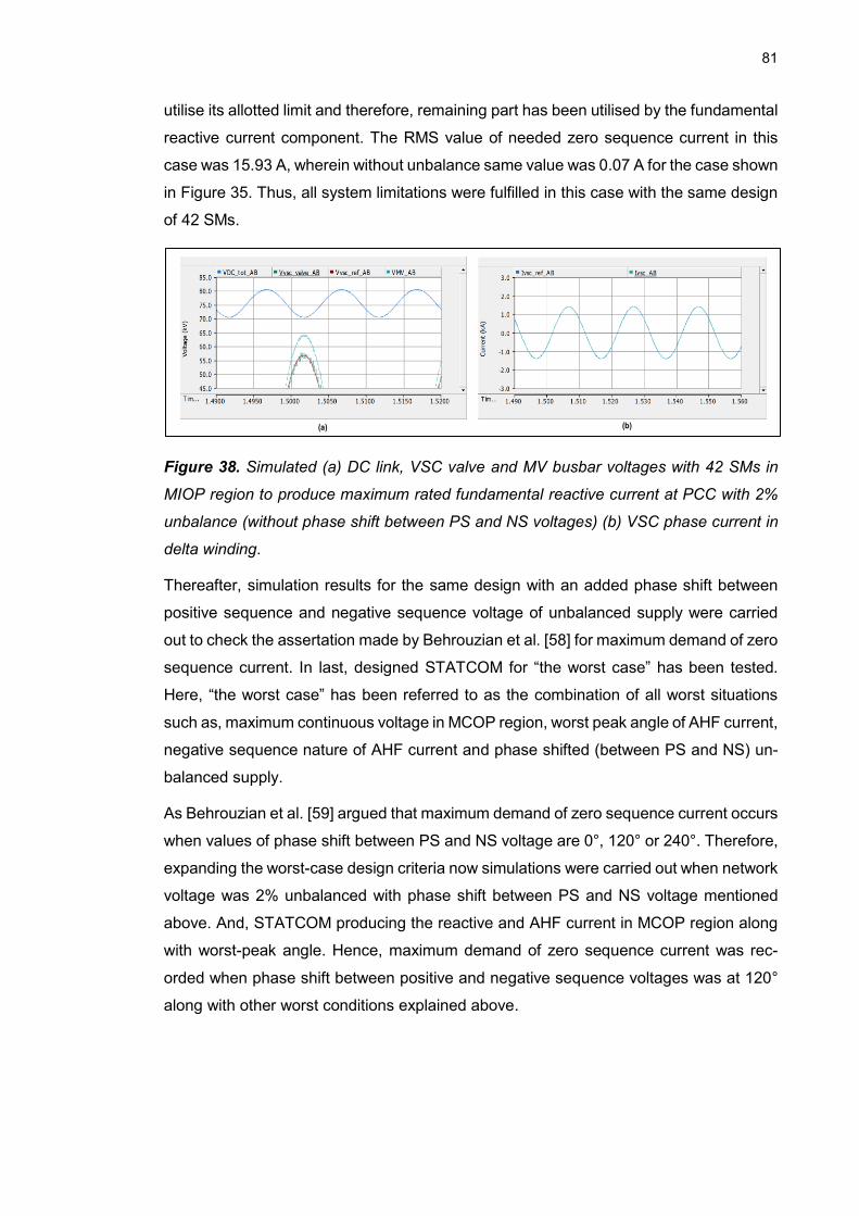
81
utilise its allotted limit and therefore, remaining part has been utilised by the fundamental
reactive current component. The RMS value of needed zero sequence current in this
case was 15.93 A, wherein without unbalance same value was 0.07 A for the case shown
in Figure 35. Thus, all system limitations were fulfilled in this case with the same design
of 42 SMs.
Figure 38. Simulated (a) DC link, VSC valve and MV busbar voltages with 42 SMs in
MIOP region to produce maximum rated fundamental reactive current at PCC with 2%
unbalance (without phase shift between PS and NS voltages) (b) VSC phase current in
delta winding.
Thereafter, simulation results for the same design with an added phase shift between
positive sequence and negative sequence voltage of unbalanced supply were carried
out to check the assertation made by Behrouzian et al. [58] for maximum demand of zero
sequence current. In last, designed STATCOM for “the worst case” has been tested.
Here, “the worst case” has been referred to as the combination of all worst situations
such as, maximum continuous voltage in MCOP region, worst peak angle of AHF current,
negative sequence nature of AHF current and phase shifted (between PS and NS) un-
balanced supply.
As Behrouzian et al. [59] argued that maximum demand of zero sequence current occurs
when values of phase shift between PS and NS voltage are 0°, 120° or 240°. Therefore,
expanding the worst-case design criteria now simulations were carried out when network
voltage was 2% unbalanced with phase shift between PS and NS voltage mentioned
above. And, STATCOM producing the reactive and AHF current in MCOP region along
with worst-peak angle. Hence, maximum demand of zero sequence current was rec-
orded when phase shift between positive and negative sequence voltages was at 120°
along with other worst conditions explained above.
(a) (b)

82
Figure 39. Simulated (a) DC link, VSC valve and MV busbar voltages with 42 SMs in
MCOP region to produce 90 A of AHF and maximum rated fundamental reactive current
at PCC, simultaneously, in worst peak situation and 2% unbalance (with 120° phase shift
between PS and NS voltages)) (b) VSC phase current in delta winding.
Figure 39(a) confirms the enough remaining DC link capacity (𝑉DC_max − 𝑉VSCrefpeak=
81.18 − 78.29 = 2.89 kV) with 42 SMs, after producing the desire current. Figure 39(b)
shows that VSC phase current remained under the defined limit of 2.1 kA of peak value.
The RMS value of needed zero sequence current in this case was 20.01 A wherein with-
out phase shift same value was 10.57 A for the case shown in Figure 37. The RMS value
of 𝐼VSC_Y was at 1686.99 A and values of fundamental reactive and AHF current at PCC
side was 262.60 A and 90.70 A respectively. Hence, all system limitations were fulfilled
with same design of 42 SMs. And, due to the unbalance network along with phase shift
of 120° between PS and NS grid voltages, increased value of zero sequence were no-
ticed.
Next simulations were carried out when network voltage was 2% unbalanced, entire
STATCOM current capacity is used to produce only reactive current in MIOP region
along with different phase shift values (e.g. 0°, 120° or 240°) of positive and negative
sequence voltage. Here, the maximum demand of zero sequence current was recorded,
when phase shift between positive and negative sequence voltages was at 240° along
with other worst conditions explained above.
Figure 40(a) validates that there was enough remaining DC link capacity (𝑉DCmin−
𝑉VSCrefpeak= 70.49 − 56.79 = 13.70 kV) with 42 SMs, after producing the desired current.
Figure 40(b) shows that VSC phase current value remained under the defined limit of
2.1 kA of the peak value. The RMS value of needed zero sequence current in this case
was 16.06 A wherein without phase shift same value was 15.93 A for the case shown in
Figure 38. The RMS value of 𝐼VSC_Y was at 1704.30 A and combined value of fundamental
reactive and AHF currents at PCC side was 284.61 A. Thus, all system limitations were
fulfilled in this case with same design of 42 SMs.
(a) (b)

83
Figure 40. Simulated (a) DC link, VSC valve and MV busbar voltages with 42 SMs in
MIOP region to produce maximum rated fundamental reactive current at PCC and 2%
unbalance (with 240° phase shift between PS and NS voltages) (b) VSC phase current
in delta winding.
In last, simulations for “the worst case” were worked out where STATCOM was produc-
ing the combined fundamental reactive and negative sequence AHF current in the MCOP
region with the worst peak angle of AHF current. And, a 2% unbalanced supply with
certain phase shift between PS and NS grid voltages. Here, maximum demand of zero
sequence was recorded when phase angle references of negative sequence AHF cur-
rent was 60° phase shifted wr.t. MV busbar voltage and phase shift between PS and NS
grid voltages was at 240°.
Figure 41. Simulated (a) DC link, VSC valve and MV busbar voltages with 42 SMs in
MCOP region to produce 90 A of negative sequence AHF and maximum rated funda-
mental reactive current at PCC, simultaneously, in worst peak situation and 2% unbal-
ance (with 240° phase shift between PS and NS voltages) (b) VSC phase current in delta
winding.
Figure 41 shows that there was enough remaining DC link capacity (𝑉DC_max −
𝑉VSCrefpeak= 83.29 − 79.35 = 3.94 kV) with 42 SMs, after producing the desired current.
Figure 41(b) shows that VSC phase current remained under the defined limit 2.1 kA of
the peak value. The RMS value of needed zero sequence current in this case was 23.52
(a) (b)
(a) (b)

84
A wherein with positive sequence AHF current same value was 20.01 A for the case
shown in Figure 39. Here, value of zero sequence current which is higher than the cal-
culated value with the equation in the beginning of this subchapter (20 A) but due to the
safety margin (rounding wye current up to 40 A) it is still within the limit. Further, the
RMS value of 𝐼VSC_Y was at 1684.32 A and the value of fundamental reactive and nega-
tive sequence AHF current at the PCC was as desired.
Finally, STATCOM design with 42 SMs has been able to produce the desired current at
PCC in all possible worst conditions. The capacity for zero sequence current to be re-
served in delta winding turned out to be approximately equals to the percent of unbalance
in the network (2% unbalanced network requires 2% capacity reservation of 1000 A). But
this applies only for the tested combination of reactive current and 3rd harmonic only.
Because with different order of harmonics, the results might be different.
4.4.5 Conservative design for case 2
In chapter 4.4.2 of case 2, it was realised that due to the geometric sum principle of
fundamental reactive current and AHF current(√𝐼Ifund_reactive
2 + 𝐼filtering2 ), the maximum of
these currents can not be achieved always at the same time. Figure 32 shows that if the
phase angle reference of AHF current are such that they cause the worst peak angle
situation of VSC voltages, then corresponding value (of desired PCC side max. reactive
and AHF current) in terms of VSC current in wye-winding exceeds its limit of 1730 A.
Moreover, Figure 33 shows that if the phase angle references of AHF current are such
that they cause the best peak angle situation of VSC voltages then corresponding value
of wye-winding VSC current remains lower than 1730 A with almost 100 A of AHF current
at the PCC but slightly less value (260.01 A) of desired (262.43 A) fundamental reactive
current. Hence, still maximum of both these currents couldn’t be achieved simultane-
ously.
Having said that, it was of interest to design a case where both maximum of fundamental
current (e.g. 262.43 A) and maximum of AHF current (e.g. 100 A) can be achieved sim-
ultaneously without compromising any of the system limitations. Hence, it was assumed
that instead of rating the VSC’s current with the geometric sum, an arithmetical sum of
fundamental reactive and AHF currents should be utilised. Because, an arithmetical sum
of RMS values of fundamental and AHF current might result in taking all current phase
angles (e.g. worst peak angle) related worst situations into the account.

85
According to chapter 4.4.2, RMS value of maximum fundamental and maximum AHF
current to be achieved at the PCC were 262.43 A and 100 A respectively. Hence, con-
sidering the conservative design, and thus their arithmetic sum, the overall primary side
PCC current would be as follows
𝐼PCC_primary = 𝐼fund_reactive + 𝐼h,max = 262.43 + 100 = 363.43 A (4.14)
In order to produce a combine AHF and reactive current of 363.43 A of magnitude, the
MVAr capacity of STATCOM should be revised as mentioned below.
𝑄STATCOM = 𝐼PCC_primary ∗ √3 ∗ 𝑉LL_primary
𝑄STATCOM = 363.43 ∗ √3 ∗ 220 ∗ 1000 = 138.10 Mvar (4.15)
Thereafter, to keep the maximum RMS value of VSC current in delta winding below 1000
A and also to consider situation of 2% unbalance supply, the maximum RMS value of
secondary side PCC current or VSC current in wye winding should be as follow
𝐼PCC_secondary or IVSC_wye = 1000 ∗ √3 − 40 = 1692.0 A (4.16)
To get this value of current, secondary side line to line PCC voltage of the transformer
should be calculated as mentioned below.
𝑉LL_secondary =𝑄STATCOM
(√3 ∗ 𝐼PCC_secondary)
𝑉LL_secondary =138.10 MVAr
(√3∗1692 A)= 47.12 kV (4.17)
In last, following the same procedure as mentioned in chapter 4.4.2, the reactance of
coupling inductor and the needed number of SMs to produce the desired current, as
calculated through equation 4.14, were carried out and worked out to be 19.49 mH and
51 SMs respectively. Thereafter, this designed STATCOM with a pessimistic or con-
servative approach was tested in “the worst” network condition, as explained in the end
of last subchapter, and respective simulation results are shown in Figure 51.
Figure 42(a) confirms the enough remaining DC link capacity (𝑉DC_max − 𝑉VSCrefpeak=
99.63 − 96.14 = 3.49 kV) with 51 SMs, after producing the desired current at PCC. Figure
42(d) shows that with conservative design (arithmetic summation of currents), the maxi-
mum RMS value of fundamental reactive current as 262.43 A and 100 A of AHF current
can be achieved simultaneously at the PCC without exceeding VSC current limit in wye
or delta winding. Here, VSC current in delta and wye winding remains well below than
1000 A and 1730 A respectively and can be validated from Figure 42(b)&(c). However,
achieving the maximum of both fundamental reactive and AHF current simultaneously

86
was not possible with an economical design (geometric summation of currents) as per
the results shown in Figure 32.
Figure 42. Simulated (a) DC link, VSC valve and MV busbar voltages with 51 SMs in
MCOP region to produce maximum rated fundamental reactive and negative sequence
AHF current at PCC simultaneously, in worst peak situation and 2% unbalance (with
240° phase shift between PS and NS voltages) (b) VSC phase current in delta winding.
Moreover, it was interesting to note that with a conservative design number of needed
SMs to produce combined 262.43 A of fundamental reactive and 100 A of AHF current
at the PCC was 51. But, with an economical design though there was slightly less current
(262.43 A fundamental and 90 A AHF) at the PCC but the number of needed SMs was
only 42. Further, in conservative design, even after producing the desired current at the
PCC, only the maximum of 772 A of overall VSC current in delta winding out of 1000 A
was utilised. And, it clearly signifies that though, a conservative design of STATCOM
with high MVAr rating and number of SMs help in achieving the maximum current objec-
tives, but it does not fully utilise its rated capacity, therefore not an optimum design.
Conclusively, an optimum design exists between economical and conservative design
which fulfills all the requirements but does not have an easy current summation principle
(arithmetical or geometrical). Since the requirements were almost achieved with geomet-
ric summation and there was a lot extra current capacity with arithmetical summation,
optimal design current summation principle is closer to the geometrical summation.
4.4.6 Summary of case 2
In chapter 4.4, a STATCOM capable of producing nominal reactive power and to perform
active harmonic filtering at the same time was designed. While designing, worst condi-
tions sought in chapter 4.3 along with the influence of minimum system impedance char-
acteristics were also considered.
(a) (d)
(b) (c)
VSC...
Ivsc_AB_r...
776.448
VSC...
Ivsc_BC_rms
742.924
VSC...
Ivsc_CA_r...
771.049
IVS...
IvscY(B)rms
1320.5
IVS...
IvscY(C)rms
1317.33
IVS...
IvscY(A)rms
1328.9
IPC...
Ipcc_fund
262.551
IPC...
Ipcc_filteri...
100.95

87
The designed STATCOM was tested with unbalanced supply, in MCOP and MIOP re-
gion, to see its effect on the required zero sequence current for the arm balancing. All
simulation results were reconciled and shown in Appendix B, Table 2. Here, it was no-
ticed that the demand of zero sequence current increases when first 2% of unbalance
along with worst peak angle reference of AHF current was introduced. Thereafter, intro-
ducing phase shift between positive and negative sequence voltages such that their
peaks are aligned resulted in further increasing the demand of zero sequence current.
In last, maximum zero sequence current was needed when simulation in MCOP region
of STATCOM with phase shifted (PS and NS peak aligned) unbalanced supply, worst
peak angle reference and negative sequence type of AHF current was worked out.
In designing process, amount of zero sequence to be reserved can be computed through
the equation mentioned chapter 4.4.4. However, it is only valid when STATCOM is op-
erating in RPC mode. After adding AHF operation, value of zero sequence current de-
pends upon the degree of unbalance, phase shift between PS and NS network voltage,
magnitude of AHF current, its phase angle and order of harmonic. Further, results of
case 2 suggested that amount of required zero sequence current was approximately
equal to the percent of unbalance (2% network unbalanced = 2%*1000 A= 20 A of zero
sequence current in delta winding). But it applies only to the AHF current magnitude,
order and phase angle used in chapter 4.4.4, and therefore value of zero sequence cur-
rent may vary with different AHF current. Moreover, demand of zero sequence current
result in decreasing the fundamental reactive current from its nominal value, due to sum-
mation principle and VSC current limitation shown in equation 4.5. Hence, to achieve the
nominal fundamental reactive current and to fulfil the zero-sequence current demand as
well, MV busbar voltage needs to be increased which further affects the reactance value
of coupling inductor, needed number of SMs and thus the overall STATCOM design.
In last, it was noticed that with an economical design (geometric reactive and harmonic
current summation) condition for maximum fundamental reactive current and maximum
filtering current can not be fulfilled at the same time, without violating VSC current limi-
tation in delta winding. However, same was possible with conservative design (arithmet-
ical reactive and harmonic current summation) at the cost of higher MVAr rating, a higher
number of needed SMs and less utilisation of overall capacity. Hence, there is an optimal
current summation principle (or optimal design) exists; something in between the afore-
mentioned geometrical and arithmetical principles, but closer to the geometric one.

88
5. FUTURE WORK
Keeping the length of this thesis in mind, there are so many other aspects and ideas
which were decided not to include in this work. To get high magnitude harmonic current,
needed to investigate the worst impact on a STATCOM design, a short-circuited network
impedance based easier approached was used in this thesis work. However, more com-
plex and rather realistic condition would be to inject the current harmonics using the grid
side voltage source in presence of a certain network impedance and then verify the
STATCOM design and its performance for active harmonic filtering and reactive current
production simultaneously.
Second, the effect of zero sequence AHF current on STATCOM design was not carried
out in this thesis because of the topology-based restrictions. Since SDBC based MMC
STATCOM was studied in this thesis where VSC branches were placed in a delta ar-
rangement. Therefore, using this topology, a zero sequence AHF current cannot be pro-
duced. Hence, SSBC based MMC STATCOM model can be used in future work to carry
out such studies.
The effect on STATCOM design when active harmonic filtering is prioritized over funda-
mental reactive current has not been investigated. Hence recommended for the future
work. Additionally, optimum summation principle for AHF and reactive current was not
found/investigated in greater details which might be needed to fulfill all requirements
without significant over dimensioning.

89
6. CONCLUSION
The main objective of this thesis was to design a STATCOM when its fundamental reac-
tive current is prioritized over active harmonic filtering and when it is required to produce
nominal fundamental reactive current/power and perform active harmonic filtering at the
same time. For such a combined RPC and AHF operation of the studied STATCOM, it
was of interest to investigate how adding AHF functionality affects its design in terms of
the needed number of SMs, DC link voltage capacity, MV busbar voltage, transformer
and coupling inductor reactance. Additionally, how to sum the fundamental and AHF
current and Impact on zero sequence current demand due to such a combined operation
in unbalance grid operation were also among those interests
Starting with the design case where RPC operation was prioritised over AHF, it was
found that producing AHF current affects the STATCOM design in three ways. First was
the magnitude of AHF current where the number of needed SMs to produce the required
voltage increases with increasing AHF current magnitude. The second was the phase
angle references of AHF current. If they are chosen such that the peaks of produced
VSC’s fundamental and harmonic voltages are aligned, then the situation of worst peak
angle occurs. In this situation, the needed number of SMs to produce the same magni-
tude of AHF current increases in comparison to the situation where VSC voltage peaks
are either not aligned or in opposite directions. The third effect on STATCOM design was
based on the order of AHF current to be produced. Here, simulation results suggested
that the number of needed SMs to produce the same magnitude of AHF current in-
creases as the order of harmonic of filtering current increases. The highest SM number
was needed when same current capacity (RMS) was used for a current of three com-
bined harmonics. Alongside, it was also found that increasing the reactance of trans-
former and coupling inductor results into increase in the needed number of SMs to pro-
duce the same amount of voltage, as with lower reactance values.
Another option for aforesaid prioritisation case (extra AHF when RPC is not needed) is
not to utilize the whole current capacity and limit the operation based on the number of
submodules needed in RPC mode only, instead not to produce so high AHF current that
number of sub-modules should be increased). This brings benefit to a network operator
most of the time without over dimensioning the STATCOM and saving significantly in
term of additional hardware costs.

90
In case of designing STATCOM capable to produce nominal reactive power and per-
forming active harmonic filtering at the same time, simulation results suggested that op-
erating with the maximum current in both operations creates a bottleneck with the overall
current limit of studied STATCOM in delta winding. Here, the maximum fundamental
reactive current and maximum filtering current can not be achieved at the same time with
an economical design (geometrical summation of currents). However, achieving maxi-
mum RMS values for both of these currents is possible in a conservative design (arith-
metical summation of currents); with a trade-off between significant safety margin of VSC
current in delta winding due to high MVAr rating (and higher cost) or optimum utilisation
of current capacity (even closer to the limit) with less MVAr rating. Hence, an optimum
design current summation principle exists between these two designs which fulfils all the
requirements and seems to be quite close to the geometrical summation principle of
economical design.
Further, testing the designed STATCOM with unbalanced supply, it was noticed that the
maximum demand of zero sequence current occurs when STATCOM was producing
fundamental reactive current and negative sequence AHF current in the MCOP region
simultaneously. And, here peaks of positive and negative sequence network voltage
were aligned along with the worst peak angle reference of AHF current. Furthermore,
when STATCOM was producing only reactive power in MIOP region, then the highest
demand of zero sequence was recorded when peaks of positive and negative sequence
network voltage were aligned.

91
REFERENCES
[1] S. R. Durdhavale and D. D. Ahire, “A Review of Harmonics Detection and Meas-urement in Power System,” International Journal of Computer Applications, vol. 143, no. 10, pp. 42–45, 2016.
[2] H. Akagi, “Active Harmonic Filters,” Proceedings of the IEEE, vol. 93, no. 12, pp. 2128–2141, 2005.
[3] N. G. Hingorani and L. Gyugyi, Understanding FACTS: Concepts and Technology of Flexible AC Transmission Systems. New York: Wiley-IEEE Press, 1999.
[4] F. C. De La Rosa, Harmonics and power systems. Boca Raton: Taylor & Francis, 2006.
[5] E. Fuchs and M. A. S. Masoum, Power Quality in Power Systems and Electrical Machines. San Diego: Elsevier Science, 2008.
[6] W. M. Grady and S. Santoso, “Understanding power system harmonics,” IEEE Power Engineering Review, vol. 21, no. 11, pp. 8–11, 2001.
[7] V. E. Wagner et al., “Effects of harmonics on equipment,” IEEE Transactions on Power Delivery, vol. 8, no. 2, pp. 672–680, 1993.
[8] A. Elmoudi, M. Lehtonen, and H. Nordman, “Effect of harmonics on transformers loss of life,” in Conference Record of the 2006 IEEE International Symposium on Electrical Insulation, 2006, pp. 408–411.
[9] G. J. Wakileh, “Harmonics in rotating machines,” Electric Power Systems Re-search, vol. 66, no. 1, pp. 31–37, 2003.
[10] N. Eghtedarpour, M. Karimi, and M. Tavakoli, “Harmonic resonance in power sys-tems - a documented case,” 2014 16th International Conference on Harmonics and Quality of Power (ICHQP), pp. 857–861, 2014.
[11] N. D. Rao, S. I. Sporea, and A. Sawma, “Analysis of resonance problems and har-monic filter design in power factor correction capacitor applications,” in Conference Proceedings. IEEE Canadian Conference on Electrical and Computer Engineering (Cat. No.98TH8341), 1998, vol. 1, pp. 293–296.
[12] M. Nasiri, M. Rostami, and Seyed Hamid Fathi, “Parallel and series harmonic res-onance prevention by anti-resonance hybrid capacitor system for power factor cor-rection,” in 2010 5th IEEE Conference on Industrial Electronics and Applications, 2010, pp. 1023–1027.
[13] S. Vlahinic, D. Brnobic, and N. Stojkovic, “Indices for Harmonic Distortion Monitor-ing of Power Distribution Systems,” in 2008 IEEE Instrumentation and Measure-ment Technology Conference, 2008, pp. 421–425.
[14] S. M. Halpin, “Comparison of IEEE and IEC harmonic standards,” in IEEE Power Engineering Society General Meeting, 2005, 2005, vol. 3, pp. 2214–2216.

92
[15] “IEEE Recommended Practice and Requirements for Harmonic Control in Electric Power Systems,” IEEE Std 519-2014 (Revision of IEEE Std 519-1992), pp. 1–29, 2014.
[16] McGranaghan and Beaulieu, “Update on IEC 61000-3-6: Harmonic Emission Limits for Customers Connected to MV, HV, and EHV,” in 2005/2006 IEEE/PES Trans-mission and Distribution Conference and Exhibition, 2006, pp. 1158–1161.
[17] “IEC TR 61000-3-6, Limits - Assessment of emission limits for the connection of fluctuating installations to MV, HV and EHV power systems,” IEC, 2008.
[18] J. Persson, “Comparing Harmonics Mitigation Techniques,” In Comsys AB, Lund, p. 6, 2014.
[19] H. A. Kazem, “Harmonic Mitigation Techniques Applied to Power Distribution Net-works,” in Advances in Power Electronics, 2013, p. 11.
[20] D. Schwanz, M. Bollen, and A. Larsson, “A review of solutions for harmonic mitiga-tion,” in 2016 17th International Conference on Harmonics and Quality of Power (ICHQP), 2016, pp. 30–35.
[21] B. Singh, A. Chandra, and K. Al-Haddad, Power Quality: Problems and Mitigation Techniques. John Wiley & Sons, 2014.
[22] J. C. Das, “Passive filters - potentialities and limitations,” IEEE Transactions on In-dustry Applications, vol. 40, no. 1, pp. 232–241, 2004.
[23] B. Singh, K. Al-Haddad, and A. Chandra, “A review of active filters for power quality improvement,” IEEE Transactions on Industrial Electronics, vol. 46, no. 5, pp. 960–971, 1999.
[24] K. HAYAFUNE, T. UESHIBA, E. MASADA, and Y. OGIWARA, “Microcomputer Controlled Active Power Filters,” Proc. of the IEEE-IECON, pp. 1221–1226, 1984.
[25] J. H. Choi, G. W. Park, and S. B. Dewan, “Standby power supply with active power filter ability using digital controller,” in Proceedings of 1995 IEEE Applied Power Electronics Conference and Exposition - APEC’95, 1995, vol. 2, pp. 783–789.
[26] Chingchi Chen and D. M. Divan, “Simple topologies for single phase AC line con-ditioning,” IEEE Transactions on Industry Applications, vol. 30, no. 2, pp. 406–412, 1994.
[27] D. A. Torrey and A. M. A. M. Al-Zamel, “Single-phase active power filters for multiple nonlinear loads,” IEEE Transactions on Power Electronics, vol. 10, no. 3, pp. 263–272, 1995.
[28] S. D. Round and N. Mohan, “Comparison of frequency and time domain neural network controllers for an active power filter,” in Proceedings of IECON ’93 - 19th Annual Conference of IEEE Industrial Electronics, 1993, vol. 2, pp. 1099–1104.
[29] Mrs. M. A. Chaudhari and Chandraprakash, “Three-phase Series Active Power Fil-ter as Power Quality Conditioner,” in 2012 IEEE International Conference on Power Electronics, Drives and Energy Systems (PEDES), 2012, pp. 1–6.

93
[30] G. W. Chang, S. K. Chen, Y. C. Chin, and W. C. Chen, “An a-b-c Reference Frame-Based Compensation Strategy for Series Active Power Filter Control,” in 2006 1ST IEEE Conference on Industrial Electronics and Applications, 2006, pp. 1–4.
[31] J. Dixon, L. Moran, J. Rodriguez, and R. Domke, “Reactive Power Compensation Technologies: State-of-the-Art Review,” Proceedings of the IEEE, vol. 93, no. 12, pp. 2144–2164, 2005.
[32] Hong Chen, “Practices of reactive power management and compensation,” in 2008 IEEE Power and Energy Society General Meeting - Conversion and Delivery of Electrical Energy in the 21st Century, 2008, pp. 1–4.
[33] O. AkwukwaegbuI and O. G. Ibe, “Concepts of Reactive Power Control and Voltage Stability Methods in Power System Network,” in IOSR Journal of Computer Engi-neering, 2013, vol. 11, pp. 15–25.
[34] X. Zhou, K. Wei, Y. Ma, and Z. Gao, “A Review of Reactive Power Compensation Devices,” in 2018 IEEE International Conference on Mechatronics and Automation (ICMA), 2018, pp. 2020–2024.
[35] A. K. Pathak, M. P. Sharma, and M. Gupta, “Static Var Compensator rating finali-zation and review of high wind penetration effect in Western Rajasthan,” in 2016 IEEE 1st International Conference on Power Electronics, Intelligent Control and En-ergy Systems (ICPEICES), 2016, pp. 1–6.
[36] R. M. Mathur and R. K. Varma, Thyristor-Based FACTS Controllers for Electrical Transmission Systems. IEEE, 2002.
[37] N. Sabai, H. N. Maung, and T. Win, “Voltage Control and Dynamic Performance of Power Transmission System Using Static Var Compensator,” in World Academy of Science, Engineering and Technology, 2008, pp. 425–429.
[38] L. L. Grigsby, Power system stability and control. Boca Raton: Taylor & Francis, 2012.
[39] GE Grid Solutions, “Static Synchronous Compensator (STATCOM) Solutions,” Broucher GEA31986, 2016. [Online]. Available: https://www.gegridsolu-tions.com/products/brochures/powerd_vtf/STATCOM_GEA31986_LR.pdf. [Ac-cessed: 17-Jul-2019].
[40] C. Schauder, “Vector analysis and control of advanced static VAr compensators,” in International Conference on AC and DC Power Transmission, 1991, pp. 266–272.
[41] C. Schauder et al., “Development of a /spl plusmn/100 MVAr static condenser for voltage control of transmission systems,” IEEE Transactions on Power Delivery, vol. 10, no. 3, pp. 1486–1496, 1995.
[42] F. Shahnia, S. Rajakaruna, and A. Ghosh, Eds., Static Compensators (STAT-COMs) in Power Systems. New York, NY: Springer, 2014.
[43] B. Singh, R. Saha, A. Chandra, and K. Al-Haddad, “Static synchronous compensa-tors (STATCOM): a review,” IET Power Electronics, vol. 2, no. 4, pp. 297–324, 2009.

94
[44] O. K. Shinde and V. R. S. V. B. Pulavarthi, “STATCOM converters and control: A review,” in 2017 International Conference on Data Management, Analytics and In-novation (ICDMAI), 2017, pp. 145–151.
[45] H. Akagi, “Classification, terminology, and application of the modular multilevel cas-cade converter (MMCC),” in The 2010 International Power Electronics Conference - ECCE ASIA -, 2010, pp. 508–515.
[46] Fang Zheng Peng, Jih-Sheng Lai, J. McKeever, and J. VanCoevering, “A multilevel voltage-source inverter with separate DC sources for static VAr generation,” in IAS ’95. Conference Record of the 1995 IEEE Industry Applications Conference Thirti-eth IAS Annual Meeting, 1995, vol. 3, pp. 2541–2548.
[47] J. Park, S. Yeo, and J. Choi, “Development of ±400Mvar World Largest MMC STAT-COM,” in 2018 21st International Conference on Electrical Machines and Systems (ICEMS), 2018, pp. 2060–2063.
[48] E. Behrouzian, “Operation and control of cascaded H-bridge converter for STAT-COM application,” PhD Thesis, Chalmers University of Technology, 2016.
[49] J. Mei, Y. Ji, X. Du, T. Ma, C. Huang, and Q. Hu, “Quasi-Fixed-Frequency Hystere-sis Current Tracking Control Strategy for Modular Multilevel Converters,” Journal of Power Electronics, vol. 14, no. 6, pp. 1147–1156, 2014.
[50] N. D. Marks, T. J. Summers, and R. E. Betz, “Challenges for capacitor voltage bal-ancing in a cascaded h-bridge StatCom utilising finite control set Model Predictive Control,” in 2013 Australasian Universities Power Engineering Conference (AUPEC), 2013, pp. 1–6.
[51] J. Honkanen, “Harmonic Performance Improvement of STATCOM,” Master Thesis, Tampere University of Technology, 2018.
[52] J. S. Pridaaa, P. Tamizharasi, and J. Baskaran, “Implementation of synchronous reference frame strategy based Shunt active filter,” in 2011 3rd International Con-ference on Electronics Computer Technology, 2011, vol. 2, pp. 240–244.
[53] J. Venkatesan and S. Natesan, “A SRF-PLL Control Scheme for DVR to Achieve Grid Synchronization and PQ Issues Mitigation in PV Fed Grid Connected System,” Circuits and Systems, vol. 7, no. 10, pp. 720–726, 2016.
[54] J. Pérez-Ramírez, V. Cárdenas, and H. Miranda, “DC-bus voltage regulation scheme for asymmetric cascade H-bridge converter working as STATCOM and ac-tive filter,” in 12th IEEE International Power Electronics Congress, 2010, pp. 21–26.
[55] R. Simpson, A. Plumpton, M. Varley, C. Tonner, P. Taylor, and X. Dai, “Press-pack IGBTs for HVDC and FACTs,” CSEE Journal of Power and Energy Systems, vol. 3, no. 3, pp. 302–310, 2017.
[56] “IEC 60071-1, Insulation co-ordination - Part 1: Definitions, principles and rules,” IEC, 2011.
[57] CIGRE Working Group 14.19, “Static synchronous compensator (STATCOM),” 1999.
95
[58] D. Basic, M. Geske, and S. Schroeder, “Limitations of the H-bridge multilevel STAT-COMs in compensation of current imbalance,” in 2015 17th European Conference on Power Electronics and Applications (EPE’15 ECCE-Europe), 2015, pp. 1–10.
[59] E. Behrouzian and M. Bongiorno, “Investigation of Negative-Sequence Injection Capability of Cascaded H-Bridge Converters in Star and Delta Configuration,” IEEE Transactions on Power Electronics, vol. 32, no. 2, pp. 1675–1683, 2017.

96
APPENDIX A: PARAMETERS OF SIMULATIONS
Appendix A, Table 1. Simulation parameters for case 1
Appendix A, Table 2. Simulation parameters for case 2

97
APPENDIX B: SIMULATION RESULT SUMMARY
Appendix B, Table 1. Summary of simulation results from case 1 (RPC operation prior-
itized over AHF)
Appendix B, Table 2. Summary of simulation results from case 2 (Full RPC support in
parallel to AHF operation)
Recommended


![contiued paugt 2fruem1 itte ida re riiumoe .ZDQ]D ... · the region, Greenburgh is con-sidering three options: Full- time online instruction, in-person in - struction with social](https://img.pdfslide.us/doc/110x75/5fac32eafcb492674000077a/contiued-paugt-2fruem1-itte-ida-re-riiumoe-zdqd-the-region-greenburgh-is.jpg)