EE5311- Digital IC DesignModule 5 - Sequential Circuit Design
Janakiraman V
Assistant ProfessorDepartment of Electrical EngineeringIndian Institute of Technology Madras
Chennai
November 8, 2017
Janakiraman, IITM EE5311- Digital IC Design, Module 5 - Sequential Circuit Design 1/52
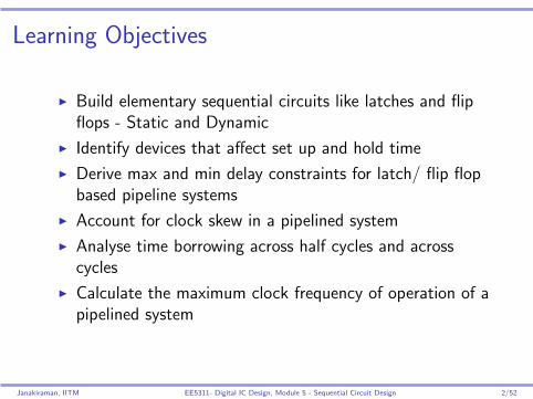
Learning Objectives
◮ Build elementary sequential circuits like latches and flipflops - Static and Dynamic
◮ Identify devices that affect set up and hold time
◮ Derive max and min delay constraints for latch/ flip flopbased pipeline systems
◮ Account for clock skew in a pipelined system
◮ Analyse time borrowing across half cycles and acrosscycles
◮ Calculate the maximum clock frequency of operation of apipelined system
Janakiraman, IITM EE5311- Digital IC Design, Module 5 - Sequential Circuit Design 2/52
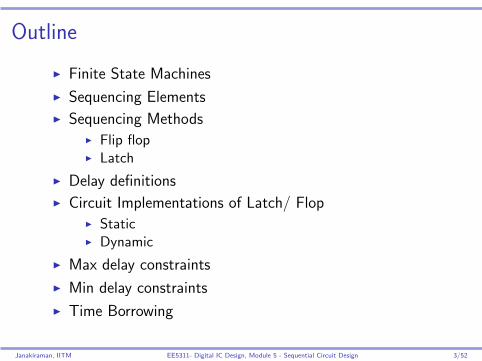
Outline
◮ Finite State Machines
◮ Sequencing Elements
◮ Sequencing Methods◮ Flip flop◮ Latch
◮ Delay definitions
◮ Circuit Implementations of Latch/ Flop◮ Static◮ Dynamic
◮ Max delay constraints
◮ Min delay constraints
◮ Time Borrowing
Janakiraman, IITM EE5311- Digital IC Design, Module 5 - Sequential Circuit Design 3/52
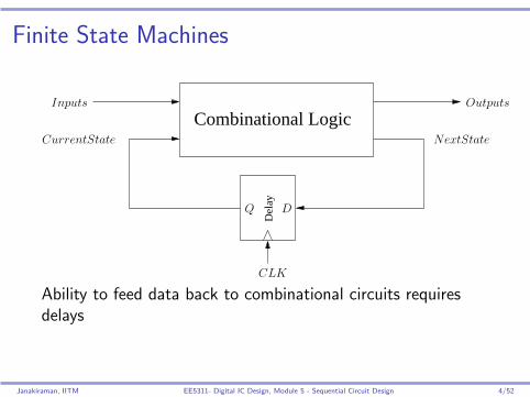
Finite State Machines
Combinational Logic
Del
ay
Inputs
DQ
Outputs
NextStateCurrentState
CLK
Ability to feed data back to combinational circuits requiresdelays
Janakiraman, IITM EE5311- Digital IC Design, Module 5 - Sequential Circuit Design 4/52
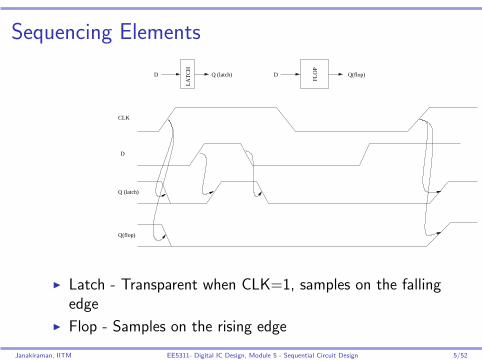
Sequencing Elements
Q(flop)
CLK
D
Q (latch)
Q(flop)
LAT
CH
FLO
P
D Q (latch) D
◮ Latch - Transparent when CLK=1, samples on the fallingedge
◮ Flop - Samples on the rising edge
Janakiraman, IITM EE5311- Digital IC Design, Module 5 - Sequential Circuit Design 5/52
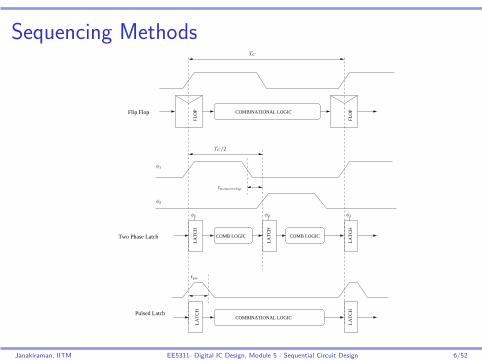
Sequencing Methods
Flip Flop COMBINATIONAL LOGIC
COMB LOGIC COMB LOGIC
FLO
P
FLO
P
LAT
CH
LAT
CH
LAT
CH
COMBINATIONAL LOGIC
LAT
CH
LAT
CHPulsed Latch
Two Phase Latch
φ1
φ2
φ1 φ2 φ1
TC
TC/2
tnonoverlap
tpw
Janakiraman, IITM EE5311- Digital IC Design, Module 5 - Sequential Circuit Design 6/52
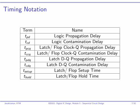
Timing Notation
Term Nametpd Logic Propagation Delaytcd Logic Contamination Delaytpcq Latch/ Flop Clock-Q Propagation Delaytccq Latch/ Flop Clock-Q Contamination Delaytpdq Latch D-Q Propagation Delaytcdq Latch D-Q Contamination Delaytsetup Latch/ Flop Setup Timethold Latch/Flop Hold Time
Janakiraman, IITM EE5311- Digital IC Design, Module 5 - Sequential Circuit Design 7/52
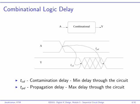
Combinational Logic Delay
Y
A Combinational Y
A
tcd
tpd
◮ tcd - Contamination delay - Min delay through the circuit
◮ tpd - Propagation delay - Max delay through the circuit
Janakiraman, IITM EE5311- Digital IC Design, Module 5 - Sequential Circuit Design 8/52
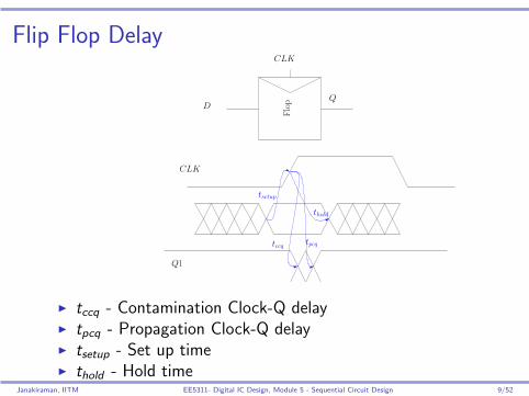
Flip Flop Delay
tsetup
CLK
D
Flop
CLK
Q
Q1
thold
tpcqtccq
◮ tccq - Contamination Clock-Q delay◮ tpcq - Propagation Clock-Q delay◮ tsetup - Set up time◮ thold - Hold time
Janakiraman, IITM EE5311- Digital IC Design, Module 5 - Sequential Circuit Design 9/52
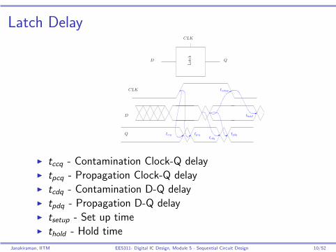
Latch Delay
tccq tpcq
CLK
D
Q
D
CLK
Q
Latch
tcdqtpdq
thold
tsetup
◮ tccq - Contamination Clock-Q delay◮ tpcq - Propagation Clock-Q delay◮ tcdq - Contamination D-Q delay◮ tpdq - Propagation D-Q delay◮ tsetup - Set up time◮ thold - Hold time
Janakiraman, IITM EE5311- Digital IC Design, Module 5 - Sequential Circuit Design 10/52
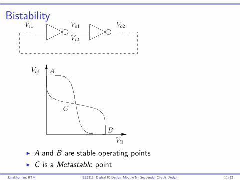
Bistability
Vi1
Vi1 Vo2Vo1
Vi2
B
A
C
Vo1
◮ A and B are stable operating points
◮ C is a Metastable point
Janakiraman, IITM EE5311- Digital IC Design, Module 5 - Sequential Circuit Design 11/52
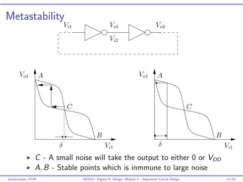
Metastability
δ
Vo2Vo1
Vi2
B
AVo1
Vi1
C
B
AVo1
Vi1δ
C
Vi1
◮ C - A small noise will take the output to either 0 or VDD
◮ A,B - Stable points which is inmmune to large noise
Janakiraman, IITM EE5311- Digital IC Design, Module 5 - Sequential Circuit Design 12/52
Switching Bistable States
◮ Breaking the Feedback loop - Multiplexer based latch
◮ Overpowering Feedback loop - Common in SRAMs
Janakiraman, IITM EE5311- Digital IC Design, Module 5 - Sequential Circuit Design 13/52
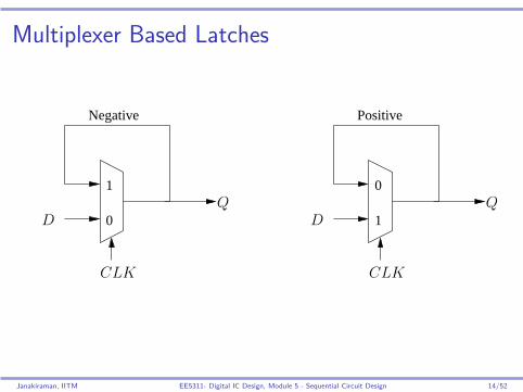
Multiplexer Based Latches
Positive
1
0
Negative
0
1
CLK
DQ
CLK
DQ
Janakiraman, IITM EE5311- Digital IC Design, Module 5 - Sequential Circuit Design 14/52

Multiplexer Based Latches
Positive
1
0
Negative
0
1
CLK
DQ
CLK
DQ
Janakiraman, IITM EE5311- Digital IC Design, Module 5 - Sequential Circuit Design 15/52
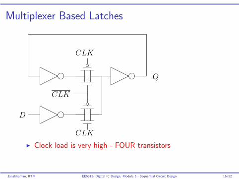
Multiplexer Based Latches
CLK
Q
CLK
D
CLK
◮ Clock load is very high - FOUR transistors
Janakiraman, IITM EE5311- Digital IC Design, Module 5 - Sequential Circuit Design 16/52
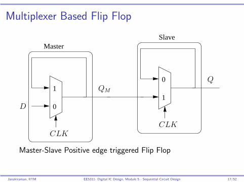
Multiplexer Based Flip Flop
Slave
1
01
0
Master
CLK
D
QM
CLK
Q
Master-Slave Positive edge triggered Flip Flop
Janakiraman, IITM EE5311- Digital IC Design, Module 5 - Sequential Circuit Design 17/52
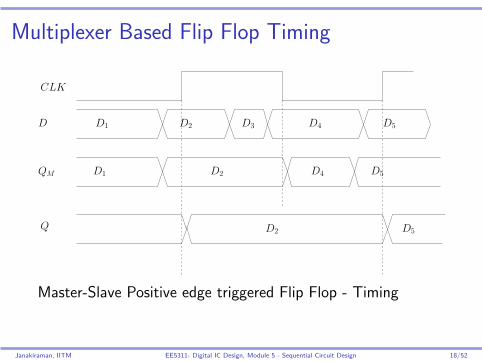
Multiplexer Based Flip Flop Timing
D4D2D1 D5
D1 D2 D5
CLK
D
QM
Q D2 D5
D3
D4
Master-Slave Positive edge triggered Flip Flop - Timing
Janakiraman, IITM EE5311- Digital IC Design, Module 5 - Sequential Circuit Design 18/52
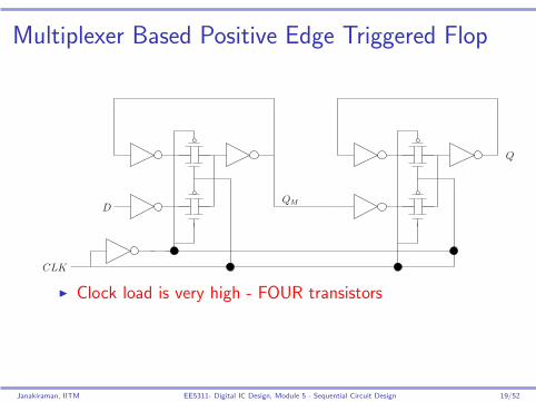
Multiplexer Based Positive Edge Triggered Flop
CLK
QMD
Q
◮ Clock load is very high - FOUR transistors
Janakiraman, IITM EE5311- Digital IC Design, Module 5 - Sequential Circuit Design 19/52
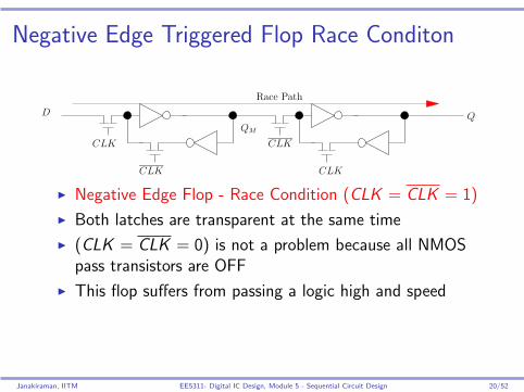
Negative Edge Triggered Flop Race Conditon
Race Path
CLK
CLK
CLK
CLK
QD
QM
◮ Negative Edge Flop - Race Condition (CLK = CLK = 1)
◮ Both latches are transparent at the same time
◮ (CLK = CLK = 0) is not a problem because all NMOSpass transistors are OFF
◮ This flop suffers from passing a logic high and speed
Janakiraman, IITM EE5311- Digital IC Design, Module 5 - Sequential Circuit Design 20/52
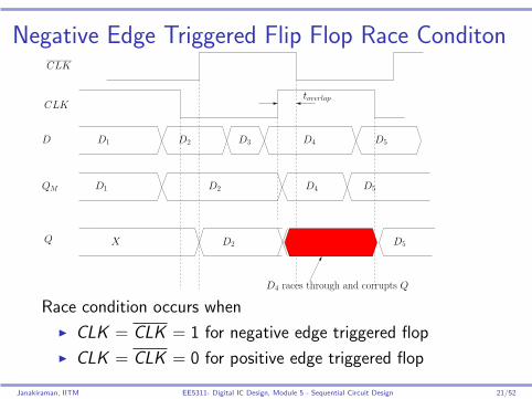
Negative Edge Triggered Flip Flop Race Conditon
X
D2D1 D5
D1 D2 D5
CLK
D
QM
Q
D3
D4
D4
CLK
D2
D4 races through and corrupts Q
D5
toverlap
Race condition occurs when
◮ CLK = CLK = 1 for negative edge triggered flop
◮ CLK = CLK = 0 for positive edge triggered flop
Janakiraman, IITM EE5311- Digital IC Design, Module 5 - Sequential Circuit Design 21/52
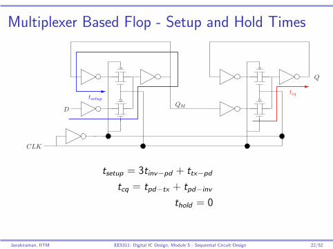
Multiplexer Based Flop - Setup and Hold Times
tcq
Q
DQM
CLK
tsetup
tsetup = 3tinv−pd + ttx−pd
tcq = tpd−tx + tpd−inv
thold = 0
Janakiraman, IITM EE5311- Digital IC Design, Module 5 - Sequential Circuit Design 22/52
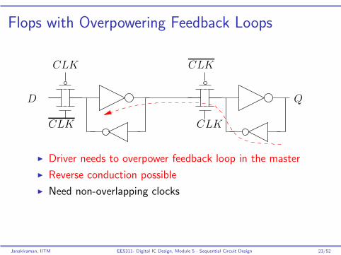
Flops with Overpowering Feedback Loops
Q
CLK
CLK
CLK
CLK
D
◮ Driver needs to overpower feedback loop in the master
◮ Reverse conduction possible
◮ Need non-overlapping clocks
Janakiraman, IITM EE5311- Digital IC Design, Module 5 - Sequential Circuit Design 23/52
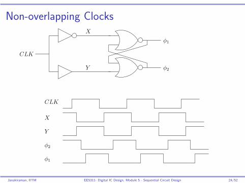
Non-overlapping Clocks
CLK
CLK
X
φ1
φ2
X
Y
Y
φ2
φ1
Janakiraman, IITM EE5311- Digital IC Design, Module 5 - Sequential Circuit Design 24/52
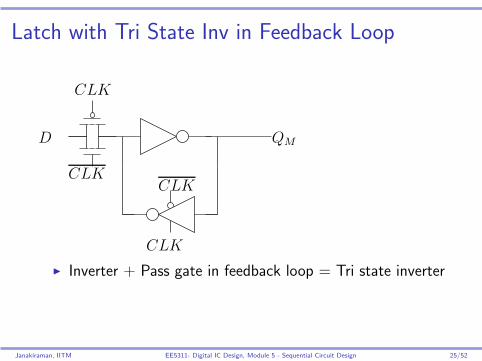
Latch with Tri State Inv in Feedback Loop
CLK
CLK
QMD
CLK
CLK
◮ Inverter + Pass gate in feedback loop = Tri state inverter
Janakiraman, IITM EE5311- Digital IC Design, Module 5 - Sequential Circuit Design 25/52
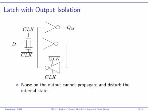
Latch with Output Isolation
QM
CLK
CLK
CLK
CLK
D
◮ Noise on the output cannot propagate and disturb theinternal state
Janakiraman, IITM EE5311- Digital IC Design, Module 5 - Sequential Circuit Design 26/52
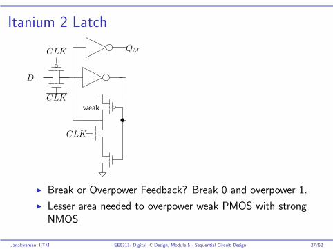
Itanium 2 Latch
weak
CLK
D
QM
CLK
CLK
◮ Break or Overpower Feedback? Break 0 and overpower 1.
◮ Lesser area needed to overpower weak PMOS with strongNMOS
Janakiraman, IITM EE5311- Digital IC Design, Module 5 - Sequential Circuit Design 27/52
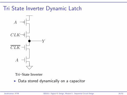
Tri State Inverter Dynamic Latch
Tri−State Inverter
A
A
Y
CLK
CLK
◮ Data stored dynamically on a capacitor
Janakiraman, IITM EE5311- Digital IC Design, Module 5 - Sequential Circuit Design 28/52
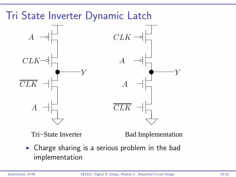
Tri State Inverter Dynamic Latch
Bad ImplementationTri−State Inverter
CLK
Y
A
A
CLK
CLK
A
A
Y
CLK
◮ Charge sharing is a serious problem in the badimplementation
Janakiraman, IITM EE5311- Digital IC Design, Module 5 - Sequential Circuit Design 29/52
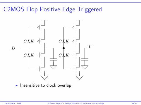
C2MOS Flop Positive Edge Triggered
YCLK
D
CLK
CLK
CLK
◮ Insensitive to clock overlap
Janakiraman, IITM EE5311- Digital IC Design, Module 5 - Sequential Circuit Design 30/52
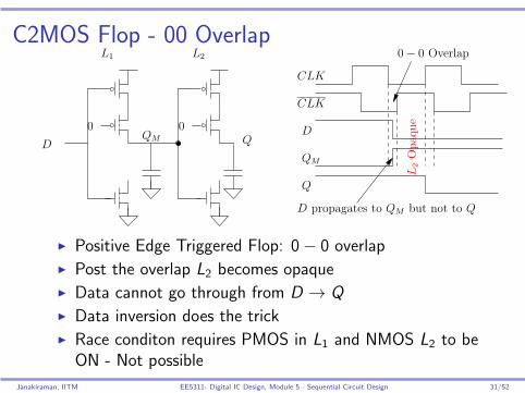
C2MOS Flop - 00 Overlap
QD
0 0
L1 L2
QM
CLK
CLK
D
0− 0 Overlap
QM
Q
L2Opaque
D propagates to QM but not to Q
◮ Positive Edge Triggered Flop: 0− 0 overlap◮ Post the overlap L2 becomes opaque◮ Data cannot go through from D → Q
◮ Data inversion does the trick◮ Race conditon requires PMOS in L1 and NMOS L2 to be
ON - Not possible
Janakiraman, IITM EE5311- Digital IC Design, Module 5 - Sequential Circuit Design 31/52
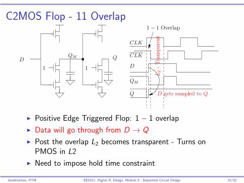
C2MOS Flop - 11 Overlap
Q CLK
CLK
D gets sampled to Q
1− 1 Overlap
D
1 1 D
QM
QM
Q
L2-Transparent
◮ Positive Edge Triggered Flop: 1− 1 overlap
◮ Data will go through from D → Q
◮ Post the overlap L2 becomes transparent - Turns onPMOS in L2
◮ Need to impose hold time constraint
Janakiraman, IITM EE5311- Digital IC Design, Module 5 - Sequential Circuit Design 32/52
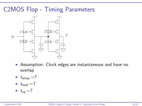
C2MOS Flop - Timing Parameters
YCLK
D
CLK
CLK
CLK
◮ Assumption: Clock edges are instantaneous and have nooverlap
◮ tsetup =?
◮ thold =?
◮ tcq =?
Janakiraman, IITM EE5311- Digital IC Design, Module 5 - Sequential Circuit Design 33/52
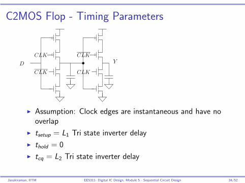
C2MOS Flop - Timing Parameters
YCLK
D
CLK
CLK
CLK
◮ Assumption: Clock edges are instantaneous and have nooverlap
◮ tsetup = L1 Tri state inverter delay
◮ thold = 0
◮ tcq = L2 Tri state inverter delay
Janakiraman, IITM EE5311- Digital IC Design, Module 5 - Sequential Circuit Design 34/52
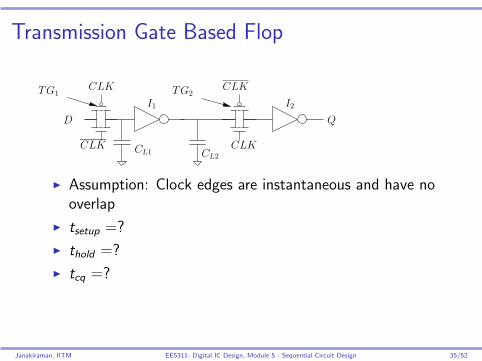
Transmission Gate Based Flop
TG1CLK CLK
CLK
D Q
CLK CL1 CL2
I2I1
TG2
◮ Assumption: Clock edges are instantaneous and have nooverlap
◮ tsetup =?
◮ thold =?
◮ tcq =?
Janakiraman, IITM EE5311- Digital IC Design, Module 5 - Sequential Circuit Design 35/52
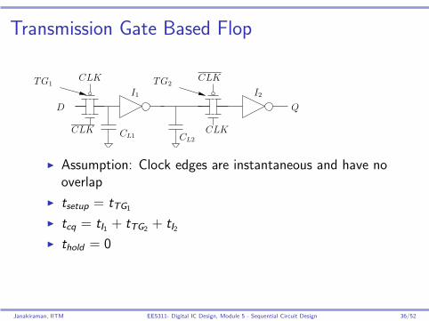
Transmission Gate Based Flop
TG1CLK CLK
CLK
D Q
CLK CL1 CL2
I2I1
TG2
◮ Assumption: Clock edges are instantaneous and have nooverlap
◮ tsetup = tTG1
◮ tcq = tI1 + tTG2 + tI2
◮ thold = 0
Janakiraman, IITM EE5311- Digital IC Design, Module 5 - Sequential Circuit Design 36/52
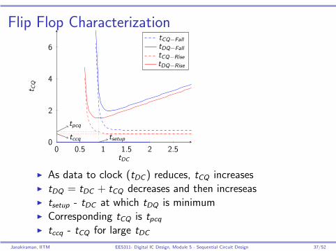
Flip Flop Characterization
0 0.5 1 1.5 2 2.50
2
4
6
tsetuptccq
tpcq
tDC
t CQ
tCQ−Fall
tDQ−Fall
tCQ−Rise
tDQ−Rise
◮ As data to clock (tDC ) reduces, tCQ increases◮ tDQ = tDC + tCQ decreases and then increseas◮ tsetup - tDC at which tDQ is minimum◮ Corresponding tCQ is tpcq◮ tccq - tCQ for large tDC
Janakiraman, IITM EE5311- Digital IC Design, Module 5 - Sequential Circuit Design 37/52
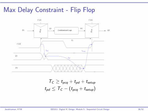
Max Delay Constraint - Flip Flop
Combinational Logic
tsetup
CLK
D1
Flop
CLK
Flop
CLK
Q2Q1 D2
Q1
D2
tpd
TC
tpcq
TC ≥ tpcq + tpd + tsetup
tpd ≤ TC − (tpcq + tsetup)
Janakiraman, IITM EE5311- Digital IC Design, Module 5 - Sequential Circuit Design 38/52
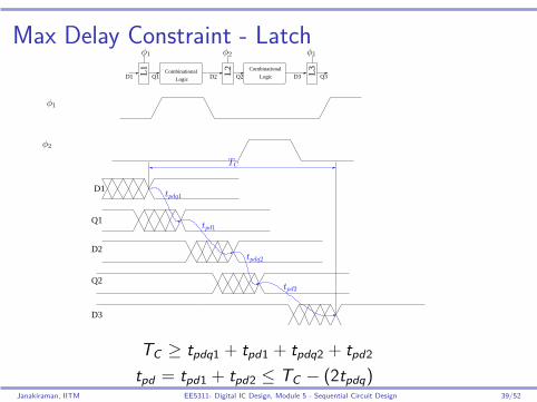
Max Delay Constraint - Latch
Logic
Combinational
Logic
D2
L1 L2 L3Q1 D2 D3Q2 Q3D1
D1
Q1
Q2
D3
Combinational
tpd2
φ1 φ2 φ1
tpdq1
tpd1
tpdq2
φ1
φ2
TC
TC ≥ tpdq1 + tpd1 + tpdq2 + tpd2
tpd = tpd1 + tpd2 ≤ TC − (2tpdq)Janakiraman, IITM EE5311- Digital IC Design, Module 5 - Sequential Circuit Design 39/52
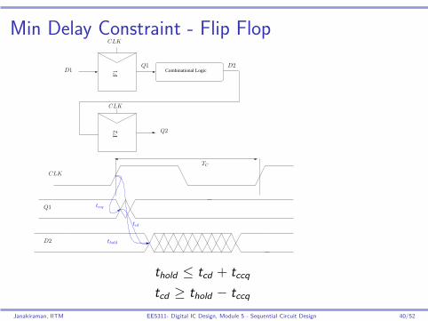
Min Delay Constraint - Flip Flop
Combinational Logic
CLK
CLK
Q1
D2
TC
thold
tccq
tcd
D1
F1
CLK
Q1 D2
F2 Q2
thold ≤ tcd + tccq
tcd ≥ thold − tccq
Janakiraman, IITM EE5311- Digital IC Design, Module 5 - Sequential Circuit Design 40/52
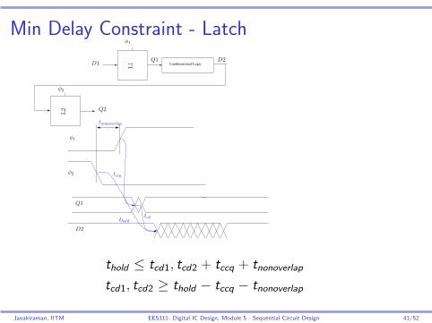
Min Delay Constraint - Latch
Combinational Logic
tnonoverlap
D1
L1
φ1
Q1 D2
Q2
L2
Q1
D2
tcd
tccq
φ2
φ1
φ2
thold
thold ≤ tcd1, tcd2 + tccq + tnonoverlap
tcd1, tcd2 ≥ thold − tccq − tnonoverlap
Janakiraman, IITM EE5311- Digital IC Design, Module 5 - Sequential Circuit Design 41/52
Time Borrowing
◮ Flops impose hard edges
◮ If data arrives late - Error
◮ If data arrives early - Data is blocked till next edge
◮ Blocking time is wasted
◮ Latches allow Time Borrowing
◮ Data doesn’t have to set up until the falling edge
Janakiraman, IITM EE5311- Digital IC Design, Module 5 - Sequential Circuit Design 42/52
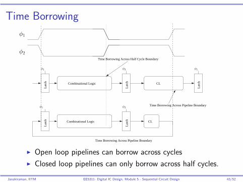
Time Borrowing
Time Borrowing Across Pipeline Boundary
Time Borrowing Across Pipeline Boundary
Time Borrowing Across Half Cycle Boundary
Combinational Logic CL
Latc
h
Latc
h
Latc
h
Combinational Logic CL
Latc
h
Latc
h
φ1
φ2
φ1
φ1
φ2 φ1
φ2
◮ Open loop pipelines can borrow across cycles
◮ Closed loop pipelines can only borrow across half cycles.
Janakiraman, IITM EE5311- Digital IC Design, Module 5 - Sequential Circuit Design 43/52
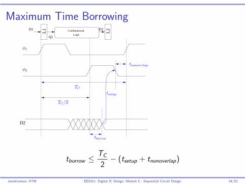
Maximum Time Borrowing
L1 Combinational
Logic
L2
D2
D2D1
Q1
φ1
φ2
TC
tnonoverlap
tsetup
tborrow
TC/2
tborrow ≤TC
2− (tsetup + tnonoverlap)
Janakiraman, IITM EE5311- Digital IC Design, Module 5 - Sequential Circuit Design 44/52
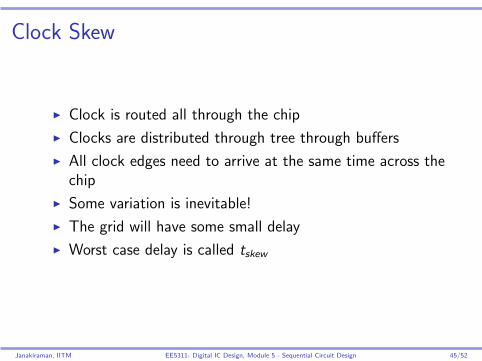
Clock Skew
◮ Clock is routed all through the chip
◮ Clocks are distributed through tree through buffers
◮ All clock edges need to arrive at the same time across thechip
◮ Some variation is inevitable!
◮ The grid will have some small delay
◮ Worst case delay is called tskew
Janakiraman, IITM EE5311- Digital IC Design, Module 5 - Sequential Circuit Design 45/52
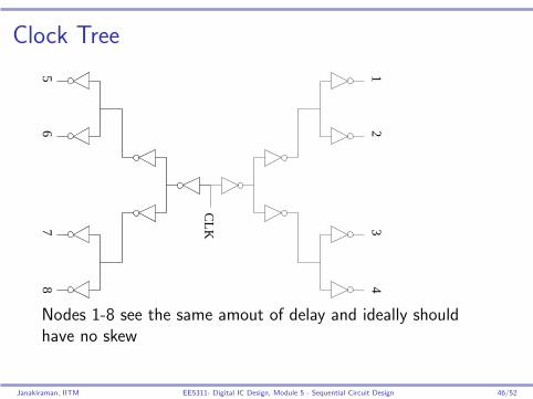
Clock Tree
87
43
CLK
21
65
Nodes 1-8 see the same amout of delay and ideally shouldhave no skew
Janakiraman, IITM EE5311- Digital IC Design, Module 5 - Sequential Circuit Design 46/52
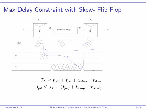
Max Delay Constraint with Skew- Flip Flop
Combinational Logic
tskew
CLK
D1
Flop
CLK
Flop
CLK
Q2Q1 D2
Q1
D2
tpd
TC
tpcq tsetup
TC ≥ tpcq + tpd + tsetup + tskew
tpd ≤ TC − (tpcq + tsetup + tskew)
Janakiraman, IITM EE5311- Digital IC Design, Module 5 - Sequential Circuit Design 47/52
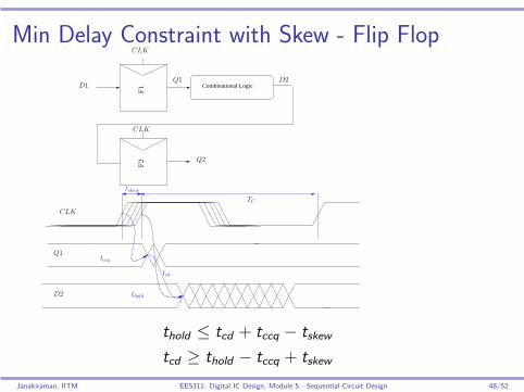
Min Delay Constraint with Skew - Flip Flop
Combinational Logic
tskew
CLK
Q1
D2
TC
thold
tcd
D1
F1
CLK
Q1 D2
F2 Q2
CLK
tccq
thold ≤ tcd + tccq − tskew
tcd ≥ thold − tccq + tskew
Janakiraman, IITM EE5311- Digital IC Design, Module 5 - Sequential Circuit Design 48/52
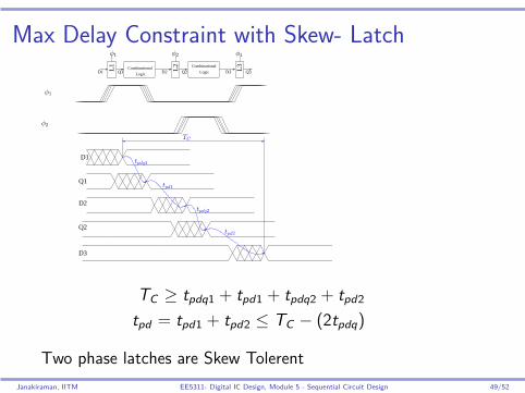
Max Delay Constraint with Skew- Latch
D2
Combinational
Logic
Combinational
Logic
D1
Q1
Q2
D3
L1 L2 L3Q1 D2 D3Q2 Q3D1
tpd2
tpdq1
tpd1
tpdq2
TC
φ1
φ2
φ1 φ2 φ1
TC ≥ tpdq1 + tpd1 + tpdq2 + tpd2
tpd = tpd1 + tpd2 ≤ TC − (2tpdq)
Two phase latches are Skew Tolerent
Janakiraman, IITM EE5311- Digital IC Design, Module 5 - Sequential Circuit Design 49/52
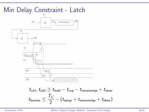
Min Delay Constraint - Latch
Combinational Logic
tskew
D1
L1
φ1
Q1 D2
Q2
L2
Q1
D2
tcd
tccq
φ2
φ1
φ2
tnonoverlap
thold
tcd1, tcd2 ≥ thold − tccq − tnonoverlap + tskew
tborrow ≤TC
2− (tsetup + tnonoverlap + tskew )
Janakiraman, IITM EE5311- Digital IC Design, Module 5 - Sequential Circuit Design 50/52
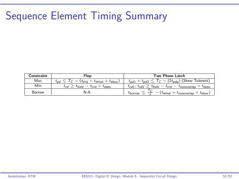
Sequence Element Timing Summary
Constraint Flop Two Phase Latch
Max tpd ≤ TC − (tpcq + tsetup + tskew ) tpd1 + tpd2 ≤ TC − (2tpdq) (Skew Tolerent)
Min tcd ≥ thold − tccq + tskew tcd1, tcd2 ≥ thold − tccq − tnonoverlap + tskew
Borrow N.A. tborrow ≤TC2
− (tsetup + tnonoverlap + tskew )
Janakiraman, IITM EE5311- Digital IC Design, Module 5 - Sequential Circuit Design 51/52
References
The material presented here is based on the following books/lecture notes
1. Digital Integrated Circuits Jan M. Rabaey, AnanthaChandrakasan and Borivoje Nikolic 2nd Edition, PrenticeHall India
2. CMOS VLSI Design, Neil H.E. Weste, David Harris andAyan Banerjee, 3rd Edition, Pearson Education
Janakiraman, IITM EE5311- Digital IC Design, Module 5 - Sequential Circuit Design 52/52
Recommended