1
EE19D Digital Electronics: Logic Devices
1
EE19D Digital Electronics
Logic Devices: Pt 1 – Decoders, Comparators, & Encoders
Covers: Comparators, Decoders, Encoders, Multiplexers, DemultiplexersRAM, ROM, PLDs - VHDL Models
EE19D Digital Electronics: Logic Devices
2
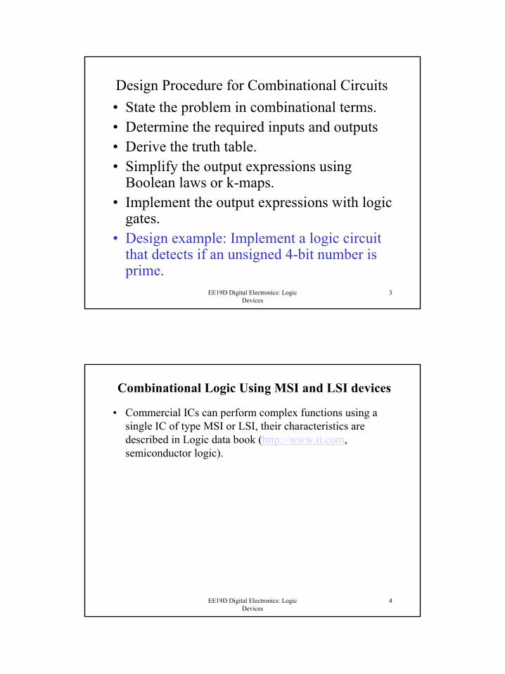
Logic Device ClassificationCombinational Circuit output is a function only of the current inputs eg., AND gates, decoders
SequentialCircuit output is a function only of the current inputs AND past inputs i.e. the circuit has memory. Eg. counters
Small Scale Integration (SSI) Integrated circuit uses only a few gates (20 or less). Typically provides only basic gate functions
Medium Scale Integration (MSI) IC uses 20-200 gates to provide common higher level functions such as decoding, multiplexing, counting etc.
Large Scale Integration (LSI) Ics have 200-200K gates ( 400K transistors) or more to realise still higher functions such as small memories and microprocessors, PLDs, CPLDs etc.
Very Large Scale Integration (VLSI) IC with over 106 transistors or more which realises the highest level of logic functionality. Examples: Pentium level processors (50 mil xsistors!),FPGAs etc.
Device delay (and cost) goes up with complexity
2
EE19D Digital Electronics: Logic Devices
3
Design Procedure for Combinational Circuits• State the problem in combinational terms.• Determine the required inputs and outputs• Derive the truth table.• Simplify the output expressions using
Boolean laws or k-maps.• Implement the output expressions with logic
gates.• Design example: Implement a logic circuit
that detects if an unsigned 4-bit number is prime.
EE19D Digital Electronics: Logic Devices
4
Combinational Logic Using MSI and LSI devices
• Commercial ICs can perform complex functions using a single IC of type MSI or LSI, their characteristics are described in Logic data book (http://www.ti.com, semiconductor logic).
3
EE19D Digital Electronics: Logic Devices
5
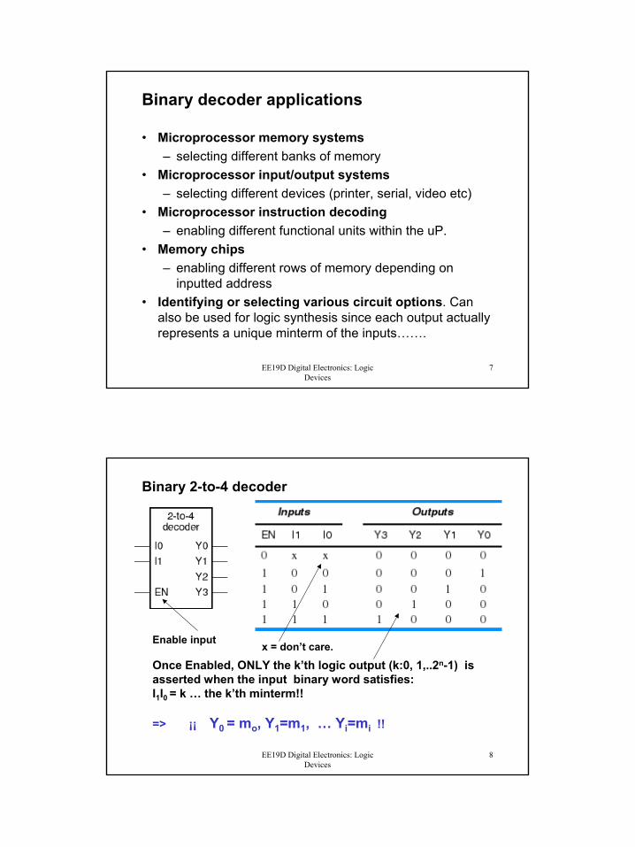
9-bit odd/even parity generator74280
BCD-to-binary converter74184
16 x 1 multiplexer74150
8 x 1 multiplexer74151
Priority encoder74147
BCD-to-Decimal encoder74145
4-line-to-16-line decoder/demultiplexer74159
3-line-to-8-line decoder/demultiplexer74137
2-line-to-4-line decoder/demultiplexer74139
4-bit magnitude comparator7485
4-bit adder with fast carry7483
DescriptionTTL Device Number
EE19D Digital Electronics: Logic Devices
6
Decoders (5.4.1-5.4.5) General decoder structure
•A decoder is a MIMO device that maps an input code to a different uniqueoutput code, I.e. the mapping is 1-to-1
• Typically n inputs, 2n
outputs 2-to-4, 3-to-8, 4-to-16, etc
• Most common: Binary Decoder maps each n-bit input to assert only 1 of 2n outputs Also: 7-segment and BCD decoders
4
EE19D Digital Electronics: Logic Devices
7
Binary decoder applications
• Microprocessor memory systems– selecting different banks of memory
• Microprocessor input/output systems– selecting different devices (printer, serial, video etc)
• Microprocessor instruction decoding– enabling different functional units within the uP.
• Memory chips– enabling different rows of memory depending on
inputted address• Identifying or selecting various circuit options. Can
also be used for logic synthesis since each output actually represents a unique minterm of the inputs…….
EE19D Digital Electronics: Logic Devices
8
Binary 2-to-4 decoder
Enable input
Once Enabled, ONLY the k’th logic output (k:0, 1,..2n-1) is asserted when the input binary word satisfies: I1I0 = k … the k’th minterm!!
=> ¡¡ Y0 = mo, Y1=m1, … Yi=mi !!
x = don’t care.
5
EE19D Digital Electronics: Logic Devices
9
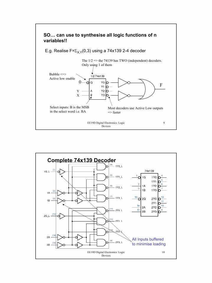
SO… can use to synthesise all logic functions of n variables!!
E.g. Realise F=ΣX,Y(0,3) using a 74x139 2-4 decoder
FYX
0
Bubble <=> Active low enable
Select inputs: B is the MSBin the select word i.e. BA
The 1/2 => the 74139 has TWO (independent) decoders. Only using 1 of them
Most decoders use Active Low outputs => faster
EE19D Digital Electronics: Logic Devices
10
Complete 74x139 Decoder
All Inputs buffered to minimise loading
6
EE19D Digital Electronics: Logic Devices
11
b2
b0b1
DEC0_LDEC1_LDEC2_LDEC3_L
DEC4_LDEC5_LDEC6_LDEC7_L
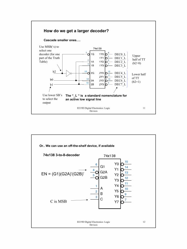
How do we get a larger decoder?
Cascade smaller ones….
Use MSB(‘s) to select one decoder (for one part of the Truth Table)
Use lower SB’s to select the output
The “_L “ is a standard nomenclature for an active low signal line
Upper half of TT (b2=0)
Lower half of TT (b2=1)
EE19D Digital Electronics: Logic Devices
12
Or.. We can use an off-the-shelf device, if available
74x138 3-to-8-decoder
C is MSB
EN = (G1)(G2A)’(G2B)’
7
EE19D Digital Electronics: Logic Devices
13
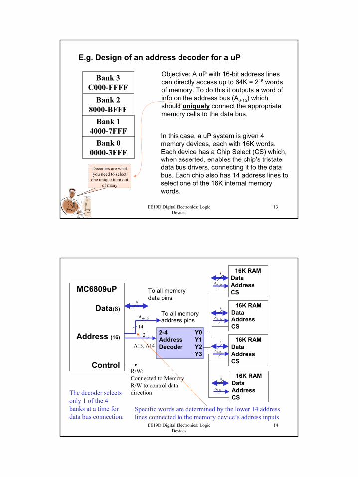
E.g. Design of an address decoder for a uP
Bank 00000-3FFF
Bank 14000-7FFF
Bank 28000-BFFF
Bank 3C000-FFFF
Objective: A uP with 16-bit address lines can directly access up to 64K = 216 words of memory. To do this it outputs a word of info on the address bus (A0-15) which should uniquely connect the appropriate memory cells to the data bus.
In this case, a uP system is given 4 memory devices, each with 16K words. Each device has a Chip Select (CS) which, when asserted, enables the chip’s tristatedata bus drivers, connecting it to the data bus. Each chip also has 14 address lines to select one of the 16K internal memory words.
Decoders are what you need to select
one unique item out of many
EE19D Digital Electronics: Logic Devices
14
MC6809uP
Data(8)
Address (16)
Control
16K RAMDataAddressCS
16K RAMDataAddressCS
16K RAMDataAddressCS
16K RAMDataAddressCS
A15, A14
2 2-4 Y0Address Y1Decoder Y2
Y3
8
To all memorydata pins
To all memoryaddress pins
A0-13
14
R/W:Connected to Memory R/W to control data directionThe decoder selects
only 1 of the 4 banks at a time for data bus connection.
Specific words are determined by the lower 14 address lines connected to the memory device’s address inputs
8
8
8
8
A0-13
A0-13
A0-13
A0-13
8
EE19D Digital Electronics: Logic Devices
15
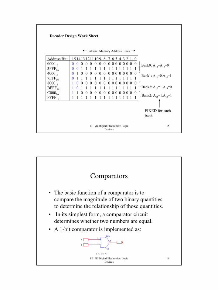
Address Bit: 15 1413 1211 10 9 8 7 6 5 4 3 2 1 0000016 0 0 0 0 0 0 0 0 0 0 0 0 0 0 0 03FFF16 0 0 1 1 1 1 1 1 1 1 1 1 1 1 1 1400016 0 1 0 0 0 0 0 0 0 0 0 0 0 0 0 07FFF16 0 1 1 1 1 1 1 1 1 1 1 1 1 1 1 1800016 1 0 0 0 0 0 0 0 0 0 0 0 0 0 0 0BFFF16 1 0 1 1 1 1 1 1 1 1 1 1 1 1 1 1C00016 1 1 0 0 0 0 0 0 0 0 0 0 0 0 0 0FFFF16 1 1 1 1 1 1 1 1 1 1 1 1 1 1 1 1
Bank0: A14=A15=0
Bank1: A15=0.A14=1
Bank2: A15=1.A14=0
Bank2: A15=1.A14=1
FIXED for each bank
Internal Memory Address Lines
Decoder Design Work Sheet
EE19D Digital Electronics: Logic Devices
16
Comparators
• The basic function of a comparator is to compare the magnitude of two binary quantities to determine the relationship of those quantities.
• In its simplest form, a comparator circuit determines whether two numbers are equal.
• A 1-bit comparator is implemented as:
B
X = 1 if A = B
X
UC1A
7433
2
31A
9
EE19D Digital Electronics: Logic Devices
17
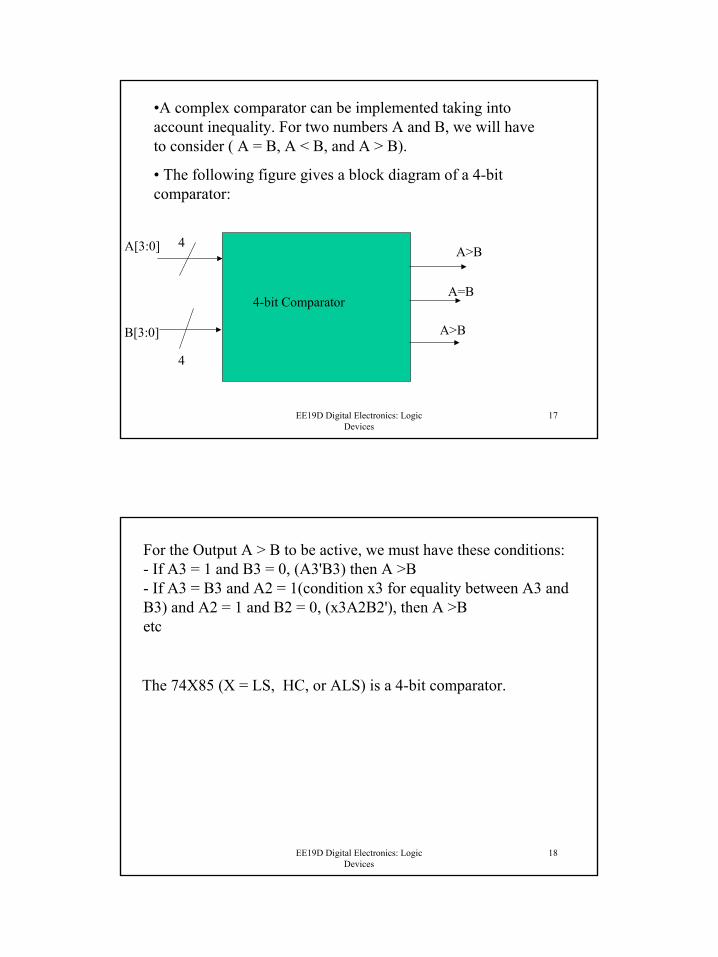
•A complex comparator can be implemented taking into account inequality. For two numbers A and B, we will have to consider ( A = B, A < B, and A > B).
• The following figure gives a block diagram of a 4-bit comparator:
4
4A[3:0]
B[3:0]
A>B
A=B
A>B
4-bit Comparator
EE19D Digital Electronics: Logic Devices
18
For the Output A > B to be active, we must have these conditions:- If A3 = 1 and B3 = 0, (A3'B3) then A >B- If A3 = B3 and A2 = 1(condition x3 for equality between A3 and B3) and A2 = 1 and B2 = 0, (x3A2B2'), then A >Betc
The 74X85 (X = LS, HC, or ALS) is a 4-bit comparator.
10
EE19D Digital Electronics: Logic Devices
19
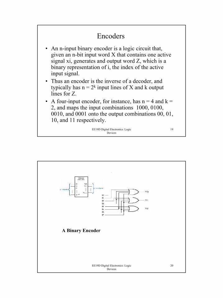
Encoders• An n-input binary encoder is a logic circuit that,
given an n-bit input word X that contains one active signal xi, generates and output word Z, which is a binary representation of i, the index of the active input signal.
• Thus an encoder is the inverse of a decoder, and typically has n = 2k input lines of X and k output lines for Z.
• A four-input encoder, for instance, has n = 4 and k = 2, and maps the input combinations 1000, 0100, 0010, and 0001 onto the output combinations 00, 01, 10, and 11 respectively.
EE19D Digital Electronics: Logic Devices
20
A Binary Encoder
11
EE19D Digital Electronics: Logic Devices
21
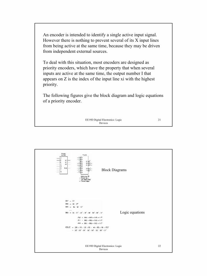
An encoder is intended to identify a single active input signal.However there is nothing to prevent several of its X input linesfrom being active at the same time, because they may be driven from independent external sources.
To deal with this situation, most encoders are designed as priority encoders, which have the property that when several inputs are active at the same time, the output number I that appears on Z is the index of the input line xi with the highest priority.
The following figures give the block diagram and logic equationsof a priority encoder.
EE19D Digital Electronics: Logic Devices
22
Block Diagrams
Logic equations
12
EE19D Digital Electronics: Logic Devices
23
EE19B Digital Electronics I
Logic Devices: Pt 2 - MultiplexersSection 5.7, Wakerly
EE19D Digital Electronics: Logic Devices
24
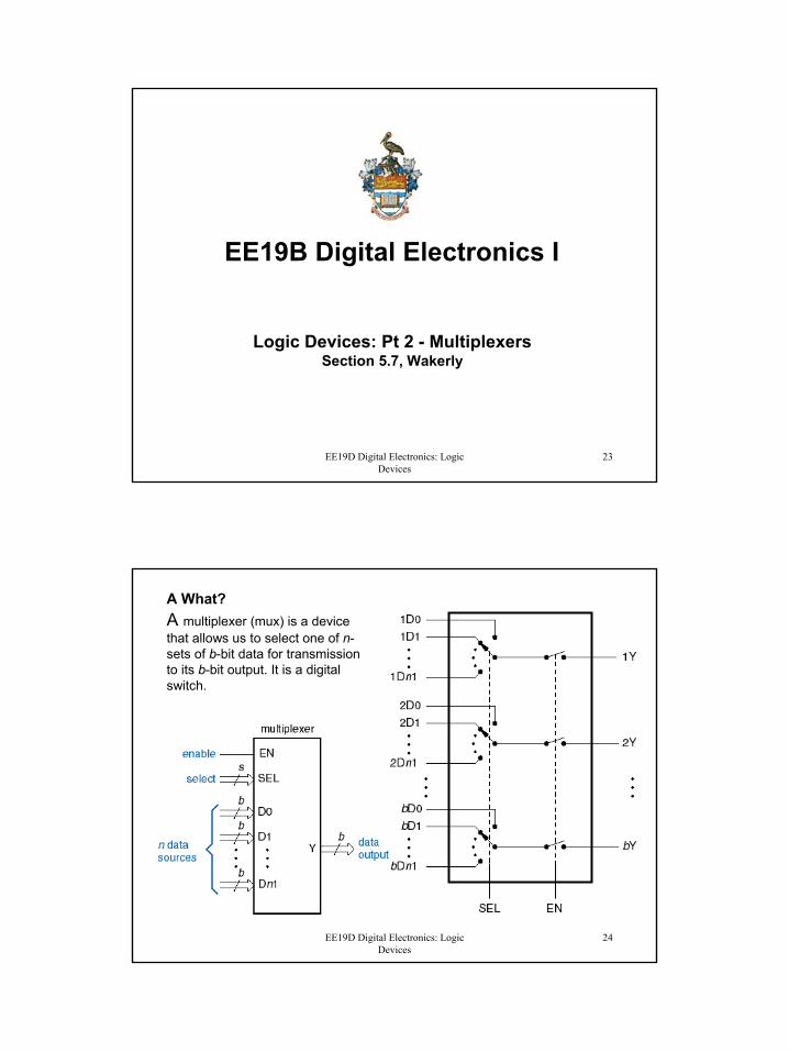
A What?A multiplexer (mux) is a device that allows us to select one of n-sets of b-bit data for transmission to its b-bit output. It is a digital switch.
13
EE19D Digital Electronics: Logic Devices
25
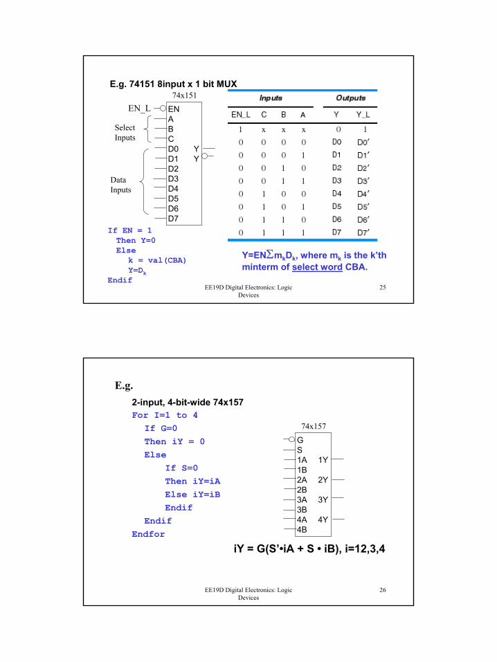
E.g. 74151 8input x 1 bit MUX
EN ABCD0 YD1 YD2D3D4D5D6D7
74x151
Select Inputs
Data Inputs
If EN = 1Then Y=0Else
k = val(CBA)Y=Dk
Endif
Y=ENΣmkDk, where mk is the k’thminterm of select word CBA.
EN_L
EE19D Digital Electronics: Logic Devices
26
2-input, 4-bit-wide 74x157For I=1 to 4
If G=0Then iY = 0Else
If S=0 Then iY=iAElse iY=iBEndif
EndifEndfor
G S1A 1Y1B2A 2Y2B3A 3Y3B4A 4Y4B
74x157
E.g.
iY = G(S’•iA + S • iB), i=12,3,4
14
EE19D Digital Electronics: Logic Devices
27
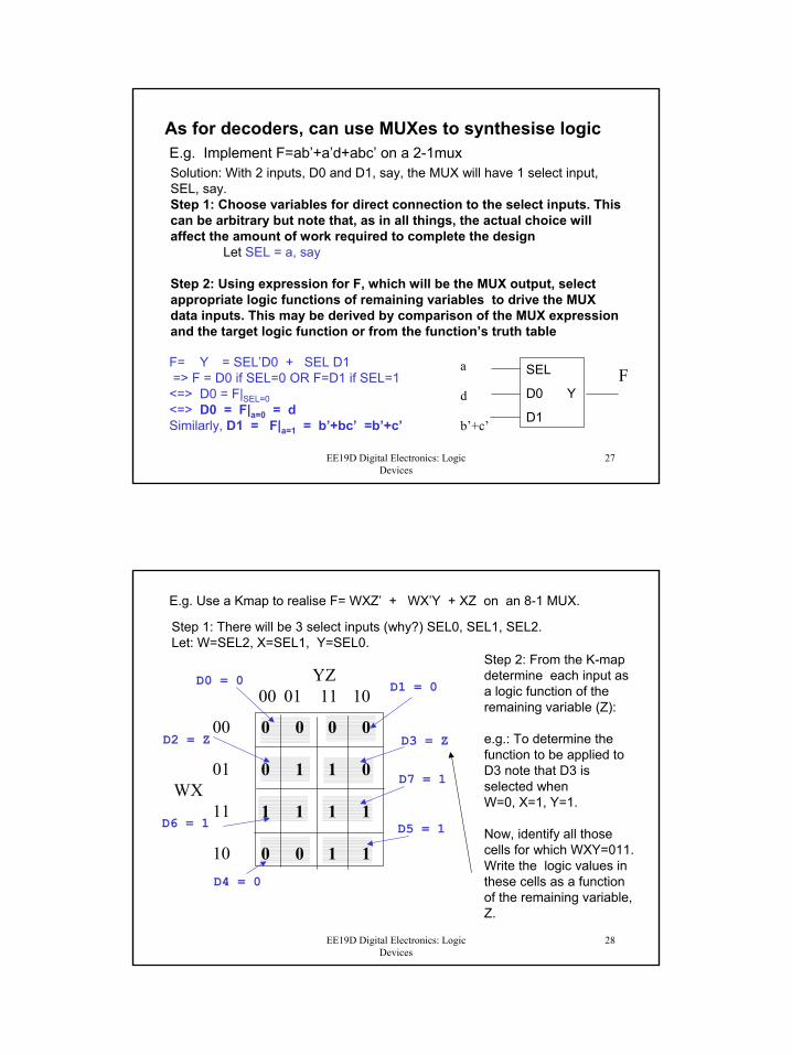
As for decoders, can use MUXes to synthesise logicE.g. Implement F=ab’+a’d+abc’ on a 2-1muxSolution: With 2 inputs, D0 and D1, say, the MUX will have 1 select input, SEL, say. Step 1: Choose variables for direct connection to the select inputs. This can be arbitrary but note that, as in all things, the actual choice will affect the amount of work required to complete the design
Let SEL = a, say
Step 2: Using expression for F, which will be the MUX output, select appropriate logic functions of remaining variables to drive the MUX data inputs. This may be derived by comparison of the MUX expression and the target logic function or from the function’s truth table
SEL
D0 Y
D1
a
d
b’+c’
FF= Y = SEL’D0 + SEL D1 => F = D0 if SEL=0 OR F=D1 if SEL=1
<=> D0 = F|SEL=0<=> D0 = F|a=0 = dSimilarly, D1 = F|a=1 = b’+bc’ =b’+c’
EE19D Digital Electronics: Logic Devices
28
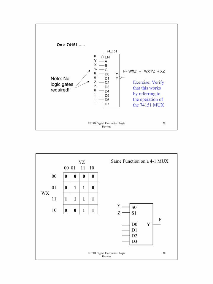
E.g. Use a Kmap to realise F= WXZ’ + WX’Y + XZ on an 8-1 MUX.
Step 1: There will be 3 select inputs (why?) SEL0, SEL1, SEL2.Let: W=SEL2, X=SEL1, Y=SEL0.
0 0 0 0
0 1 1 0
1 1 1 1
0 0 1 1
00
01WX
11
10
YZ00 01 11 10
D0 = 0 D1 = 0
D3 = Z
D7 = 1
D5 = 1
D4 = 0
D2 = Z
D6 = 1
Step 2: From the K-map determine each input as a logic function of the remaining variable (Z):
e.g.: To determine the function to be applied to D3 note that D3 is selected when W=0, X=1, Y=1.
Now, identify all those cells for which WXY=011. Write the logic values in these cells as a function of the remaining variable, Z.
15
EE19D Digital Electronics: Logic Devices
29
EN ABCD0 YD1 YD2D3D4D5D6D7
74x1510YXW00ZZ0111
F= WXZ’ + WX’YZ + XZ
On a 74151 …..
Note: No logic gates required!!
Exercise: Verify that this works by referring to the operation of the 74151 MUX
EE19D Digital Electronics: Logic Devices
30
0 0 0 0
0 1 1 0
1 1 1 1
0 0 1 1
00
01WX
11
10
YZ00 01 11 10
S0S1
D0 YD1D2D3
YZ
F
Same Function on a 4-1 MUX
16
EE19D Digital Electronics: Logic Devices
31
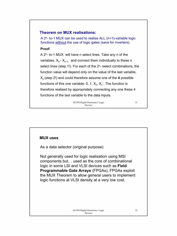
Theorem on MUX realisations:A 2n- to-1 MUX can be used to realise ALL (n+1)-variable logic functions without the use of logic gates (save for inverters).
Proof:A 2n- to-1 MUX will have n select lines. Take any n of the
variables, X0 - Xn-1, and connect them individually to these n
select lines (step 1!). For each of the 2n- select combinations, the
function value will depend only on the value of the last variable,
Xn (step 2!) and could therefore assume one of the 4 possible
functions of this one variable: 0, 1, Xn, Xn’. The function is
therefore realised by appropriately connecting any one these 4
functions of the last variable to the data inputs.
EE19D Digital Electronics: Logic Devices
32
MUX uses
As a data selector (original purpose)
Not generally used for logic realisation using MSI components but… used as the core of combinational logic in some LSI and VLSI devices such as Field Programmable Gate Arrays (FPGAs). FPGAs exploit the MUX Theorem to allow general users to implement logic functions at VLSI density at a very low cost.
17
EE19D Digital Electronics: Logic Devices
33
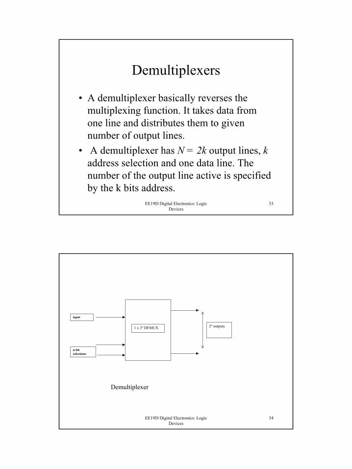
Demultiplexers
• A demultiplexer basically reverses the multiplexing function. It takes data from one line and distributes them to given number of output lines.
• A demultiplexer has N = 2k output lines, k address selection and one data line. The number of the output line active is specified by the k bits address.
EE19D Digital Electronics: Logic Devices
34
2n outputs
n-bit selections
input
1 x 2n DEMUX
Demultiplexer
18
EE19D Digital Electronics: Logic Devices
35
EE19B Digital Electronics I
Logic Devices: Pt 3 – ROMs and RAMs
EE19D Digital Electronics: Logic Devices
36
Definition
• A logic memory device allows for the storage of bits of data for later retrieval through the device output.
• Bits are retained even when the input causing them to be generated is removed
• Hence the memory device output is not a function of the immediate input but of present and past inputs.
e.g. magnetic media: memory via retention of magnetic polarityCD ROMs: memory via physical creation of pits Semiconductor memory via retention of charge
19
EE19D Digital Electronics: Logic Devices
37
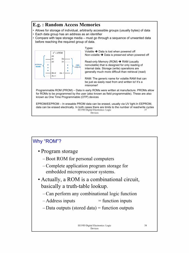
E.g. : Random Access Memories• Allows for storage of individual, arbitrarily accessible groups (usually bytes) of data• Each data group has an address as an identifier • Compare with tape storage media – must go through a sequence of unwanted data
before reaching the required group of data.
Types:Volatile Data is lost when powered off Non-volatile Data is preserved when powered off
Read-only Memory (ROM) RAM (usually nonvolatile) that is designed for only reading of internal data. Storage (write) operations are generally much more difficult than retrieval (read)
RAM: The generic name for volatile RAM that can be just as easily read from and written to! It’s a misnomer!
Programmable ROM (PROM) – Data in early ROMs were written at manufacture. PROMs allow for ROMs to be programmed by the user (also known as field programmable). These are also known as One Time Programmable (OTP) devices
EPROM/EEPROM – In erasable PROM data can be erased, usually via UV light.In EEPROM, data can be erased electrically. In both cases there are limits to the number of read/write cycles
EE19D Digital Electronics: Logic Devices
38
Why “ROM”?
• Program storage– Boot ROM for personal computers– Complete application program storage for
embedded microprocessor systems.• Actually, a ROM is a combinational circuit,
basically a truth-table lookup.– Can perform any combinational logic function– Address inputs = function inputs– Data outputs (stored data) = function outputs
20
EE19D Digital Electronics: Logic Devices
39
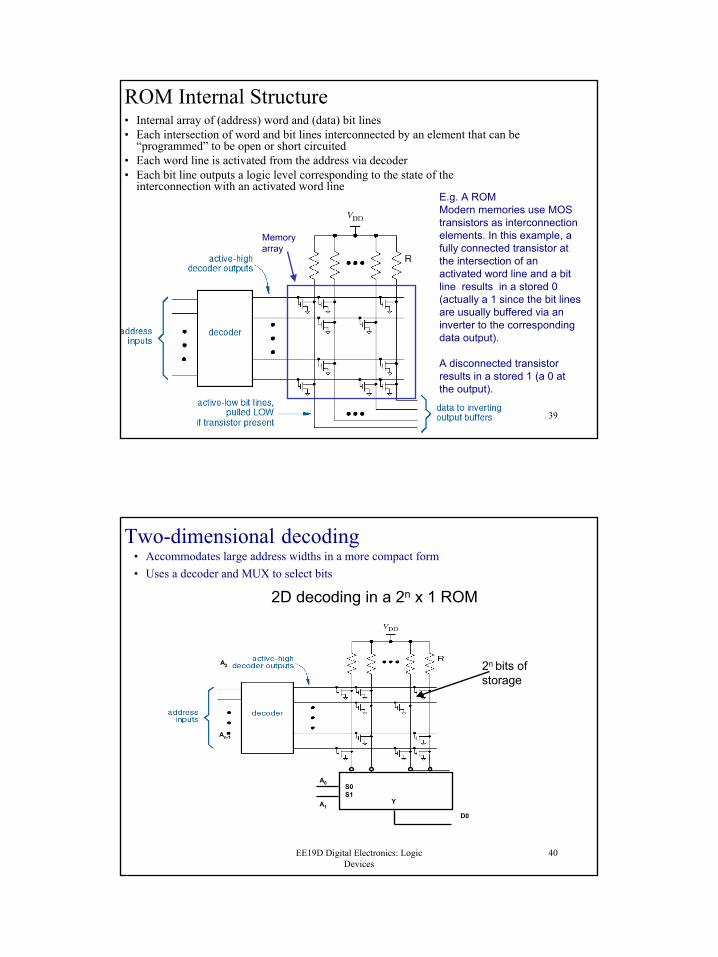
ROM Internal Structure• Internal array of (address) word and (data) bit lines• Each intersection of word and bit lines interconnected by an element that can be
“programmed” to be open or short circuited• Each word line is activated from the address via decoder• Each bit line outputs a logic level corresponding to the state of the
interconnection with an activated word line
Memory array
E.g. A ROMModern memories use MOS transistors as interconnection elements. In this example, a fully connected transistor at the intersection of an activated word line and a bit line results in a stored 0 (actually a 1 since the bit lines are usually buffered via an inverter to the corresponding data output).
A disconnected transistor results in a stored 1 (a 0 at the output).
EE19D Digital Electronics: Logic Devices
40
Two-dimensional decoding• Accommodates large address widths in a more compact form• Uses a decoder and MUX to select bits
S0S1
A0
A1Y
D0
A2
An-1
2D decoding in a 2n x 1 ROM
2n bits of storage
21
EE19D Digital Electronics: Logic Devices
41
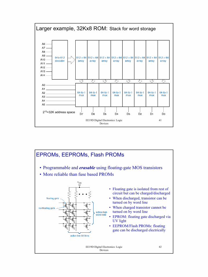
Larger example, 32Kx8 ROM: Stack for word storage
215=32K address space
EE19D Digital Electronics: Logic Devices
42
• Programmable and erasable using floating-gate MOS transistors• More reliable than fuse based PROMs
EPROMs, EEPROMs, Flash PROMs
• Floating gate is isolated from rest of circuit but can be charged/discharged
• When discharged, transistor can be turned on by word line
• When charged transistor cannot be turned on by word line
• EPROM: floating gate discharged via UV light
• EEPROM/Flash PROMs: floating gate can be discharged electrically
22
EE19D Digital Electronics: Logic Devices
43
Typical commercial EPROMs
EE19D Digital Electronics: Logic Devices
44
EEPROM programming
• Apply a higher voltage to force bit change– E.g., VPP = 12 V
• Various bit erase procedures– Byte-byte– Entire chip (“flash”)– One block (typically 32K - 66K bytes) at a time
• Programming and erasing are a lot slower than reading (milliseconds vs. 10’s of nanoseconds)
23
EE19D Digital Electronics: Logic Devices
45
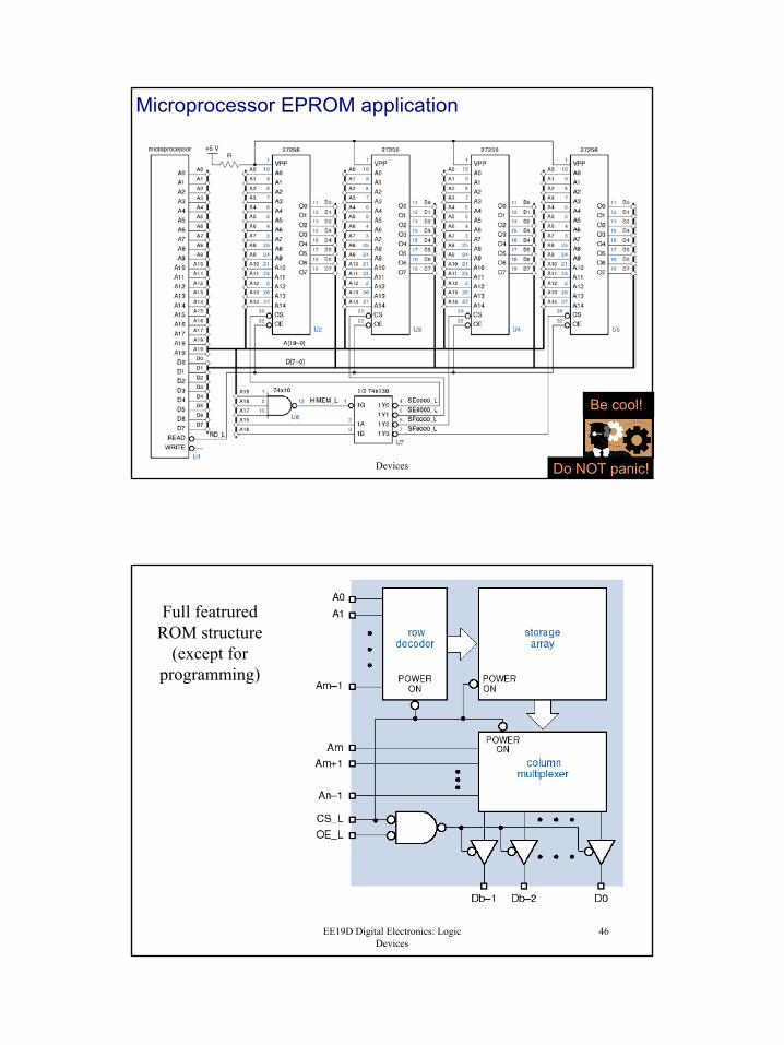
Microprocessor EPROM application
Be cool!
Do NOT panic!
EE19D Digital Electronics: Logic Devices
46
Full featruredROM structure
(except for programming)
24
EE19D Digital Electronics: Logic Devices
47
Logic-in-ROM example:2-4 Decoder with polarity control
EE19D Digital Electronics: Logic Devices
48
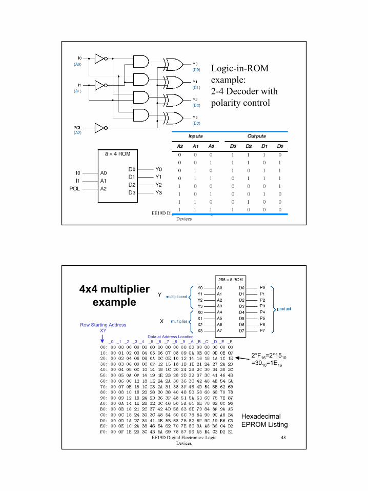
4x4 multiplier example
Y
HexadecimalEPROM Listing
Row Starting AddressXY
X
Data at Address Location_0 _1 _2 _3 _4 _5 _6 _7 _8 _9 _A _B _C _D _E _F
2*F16=2*1510=3010=1E16
25
EE19D Digital Electronics: Logic Devices
49
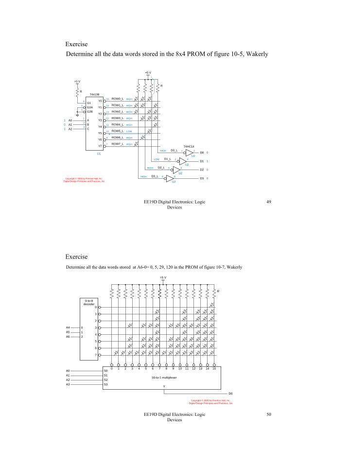
ExerciseDetermine all the data words stored in the 8x4 PROM of figure 10-5, Wakerly
D0 0
1
0
0
D2
D3
+5 V
+5 V
U1
74x138
ROW0_L HIGH
HIGH
HIGH
HIGH
HIGH
LOW
HIGH
HIGH
R
R
ROW1_L
ROW2_L
ROW3_L
ROW4_L
ROW5_L
ROW6_L
ROW7_L74HC14
D0_L
D1_L
D2_L
D3_L
G2A
G1
G2B
Y0
Y1
Y2
Y3
615
14
13
1
3
5
9 8
6
4
2
4
5
B
A
C
A1
A01
0
1 A2Y4
Y5
Y6
Y7
1 12
11
10
9
7
2
3
D1
U2
U2
U2
U2
HIGH
LOW
HIGH
HIGHCopyright © 2000 by Prentice Hall, Inc.�
Digital Design Principles and Practices, 3/e
EE19D Digital Electronics: Logic Devices
50
ExerciseDetermine all the data words stored at A6-0= 0, 5, 29, 120 in the PROM of figure 10-7, Wakerly
+5 V
3-to-8decoder
0
1
2
3
1
0
2
A5
A4
A6
A1
A0
A2
A3
S116-to-1 multiplexer
D0
Y
S0
S2
S3
4
5
6
7
R
0 1 2 3 4 5 6 7 8 9 10 11 12 13 14 15
Copyright © 2000 by Prentice Hall, Inc.�Digital Design Principles and Practices, 3/e
26
EE19D Digital Electronics: Logic Devices
51
EE19B Digital Electronics I
Logic Devices pt4: PLDs Wakerly Section 5.3
EE19D Digital Electronics: Logic Devices
52
Programmable Logic Arrays (PLAs)• Any combinational logic function can be realized
as a sum of products.• Idea: Build a large AND-OR array with lots of
inputs and product terms, and programmable connections.– n inputs
• AND gates have 2n inputs -- true and complement of each variable.
– m outputs, driven by large OR gates• Each AND gate has a programmable connection to each
output’s OR gate.– p AND gates where (p<<2n= no. minterms)
27
EE19D Digital Electronics: Logic Devices
53
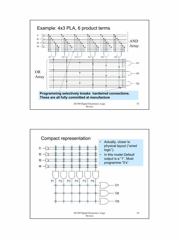
Example: 4x3 PLA, 6 product terms
Programming selectively breaks hardwired connections. These are all fully committed at manufacture
AND Array
OR Array
EE19D Digital Electronics: Logic Devices
54
Compact representation• Actually, closer to
physical layout (“wired logic”).
• In this model Default output is a “1”. Must programme “0’s”
28
EE19D Digital Electronics: Logic Devices
55
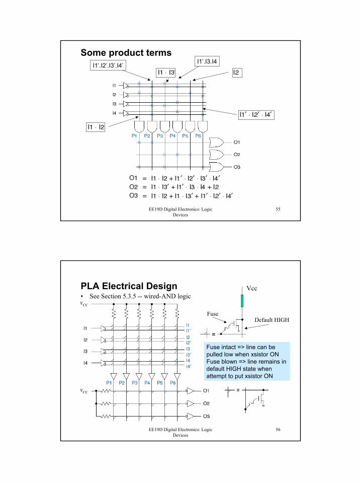
Some product termsI1’.I2’.I3’.I4’
I1’.I3.I4
EE19D Digital Electronics: Logic Devices
56
PLA Electrical Design• See Section 5.3.5 -- wired-AND logic
Fuse
Fuse intact => line can be pulled low when xsistor ONFuse blown => line remains in default HIGH state when attempt to put xsistor ON
Vcc
Default HIGH
29
EE19D Digital Electronics: Logic Devices
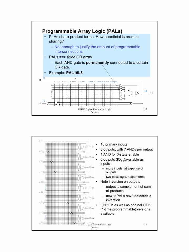
57
Programmable Array Logic (PALs)• PLAs share product terms. How beneficial is product
sharing?– Not enough to justify the amount of programmable
interconnections• PALs ==> fixed OR array
– Each AND gate is permanently connected to a certain OR gate.
• Example: PAL16L8
EE19D Digital Electronics: Logic Devices
58
• 10 primary inputs• 8 outputs, with 7 ANDs per output• 1 AND for 3-state enable• 6 outputs (IO1-6)available as
inputs – more inputs, at expense of
outputs– two-pass logic, helper terms
• Note inversion on outputs– output is complement of sum-
of-products– newer PALs have selectable
inversion• EPROM as well as original OTP
(1-time programmable) versions available

30
EE19D Digital Electronics: Logic Devices
59
Designing with PALs
• Compare number of inputs and outputs of the problem with available resources in the PAL.
• Write equations for each output using VHDL.• Compile the program, determine whether
minimized equations fit in the available AND terms.
• If no fit, try modifying equations or providing “helper” terms.
Recommended