ECE 477 Design ReviewTeam 2 Spring 2010
Digi-Brush
Josh Long Caleb Ayew-ewKatie Schremser
Outline• Project overview • Project-specific success criteria• Block diagram• Component selection rationale• Packaging design• Schematic and theory of operation• PCB layout• Software design/development status• Project completion timeline• Questions / discussion

Project Overview• Child’s toy that can eliminate the mess and stress
of children painting.• User can use multiple colors by mixing 8 given
colors • Current color will be indicated through an LED in
the tip of the brush• Painting will be recognized by interaction with a
15” touch screen • Image on the display can be saved onto an SD
Card

Project-Specific Success Criteria
1. An ability to display images on the display board2. An ability to track the digital brush on the
display board3. An ability to mimic paintbrush stroke
characteristics on the display board4. An ability to save the painted image on a SD
card5. An ability to distinguish user’s color selection
and display selected color before being painted

Block Diagram

Microcontroller :Freescale 9S12DP512DGV1
• 16-bit CPU (HCS12)• 512 kB Flash EEPROM (Program Memory)• Multiple Peripherals
– 3 SPI (FPGA)– 2 8-channel, 10-bit ATD (Color pots, Touch Screen,
Force Resistor)– 1 IIC (LED Driver)
• Max Frequency of 50 MHz (with external oscillator)• 5V Operation

FPGA: Cyclone II EP2C20Q240C8 K ABB9Y0737A• 4 PLLs• 239,616 total RAM bits• 26 Embedded Multipliers• 3.3V , Max 260 MHz Operation• Easily Accessible VHDL Libraries• Low Cost

15” Touch Monitor/Touch Screen• 15” Size
– Comparable to an 8.5” x 11” piece of paper– Cheaper than 12.1” for both parts combined
• 15” Touch Monitor– Separate Monitor and Touch Screen were cheaper than a
pre-packaged touch screen
• 15” 5-Wire Resistive Touch Screen– Resistive technology allows recognition by items other
than fingers– 5-Wire allows more accuracy than 4-Wire

Packaging Design
8 Color pots 1 “Water” Pot
15” LCD Monitor15” Touch Screen
Save/Clear Buttons
Brush Holder/Connector

Theory of Operation• Power• Microcontroller
– LED Driver– Color Pots– Force Resistor– Touch Panel
• FPGA– Boot Chip– SDRAM– VDAC/Monitor– SD Card Reader

Theory of Operation: Power
• 31V @ 2.4A inputs to linear regulators from a wall-wart
• Three LM350 Linear Regulators– >=28V to:
• 1.25V• 3.3V• 5V

Theory of Operation: Power Schematic
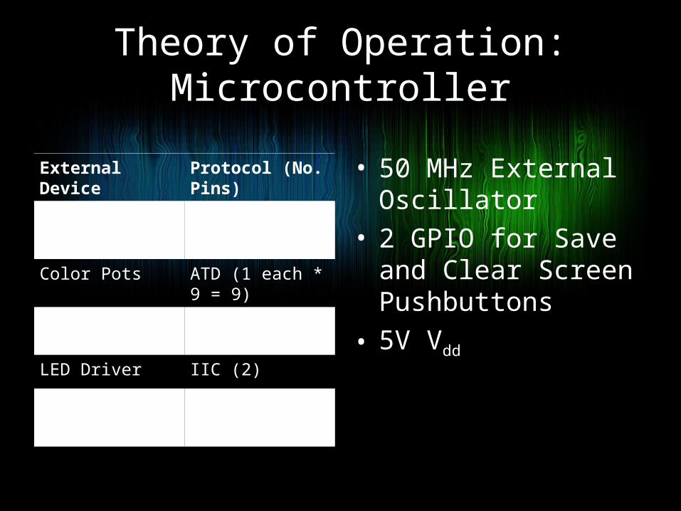
Theory of Operation: Microcontroller
External Device Protocol (No. Pins)
FPGA SPI (4)GPIO (4)
Color Pots ATD (1 each * 9 = 9)
Force Resistor ATD (1)
LED Driver IIC (2)
Touch Screen ATD (1)GPIO (4)
• 50 MHz External Oscillator
• 2 GPIO for Save and Clear Screen Pushbuttons
• 5V Vdd

Theory of Operation: Microcontroller Schematic

LED Driver
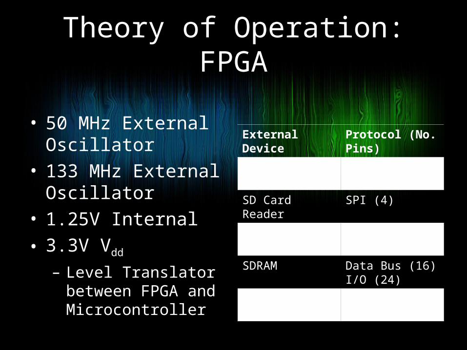
Theory of Operation: FPGA
• 50 MHz External Oscillator
• 133 MHz External Oscillator
• 1.25V Internal• 3.3V Vdd
– Level Translator between FPGA and Microcontroller
External Device Protocol (No. Pins)
Microcontroller SPI (4)GPIO (4)
SD Card Reader SPI (4)
VDAC Parallel Bus (33)
SDRAM Data Bus (16)I/O (24)
Boot Chip Digital I/O (5)

Theory of Operation:FPGA Schematic

VDAC, Boot Chip, Level Translator

SDRAM

PCB Layout: Considerations
• Separation of Analog and Digital• Large Traces for Power and GND
– Copper Pour for GND
• Many Decoupling Capacitors• Valid Trace Placements• Room for Expansion (Headers) if needed
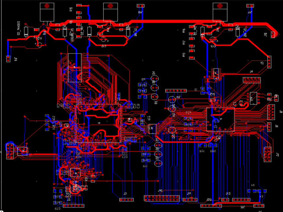
PCB Layout: Overall
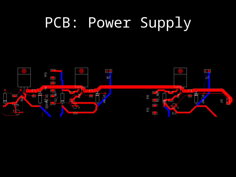
PCB: Power Supply
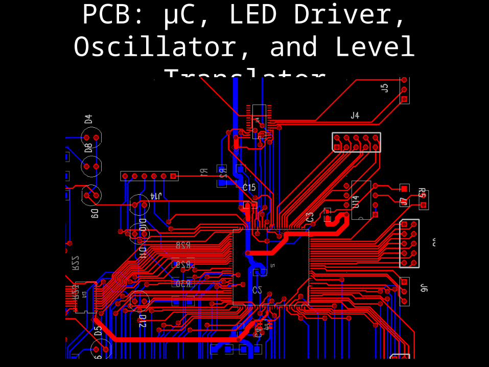
PCB: µC, LED Driver, Oscillator, and Level Translator

PCB: FPGA

PCB: VDAC, Boot Chip

PCB: SDRAM


Software Design/Development Status
• Functional Proof of Concept for mixing colors created using Java
• Programming Microcontroller with Freescale CodeWarrior and P&E BDM Multilink– Using to simulate interrupts and simple programs
relevant to the project
• Have access to SPI, VDAC, and SDRAM VHDL Libraries for the FPGA

Project Completion Timeline

Questions / DiscussionQuestions / Discussion
Recommended