Federal Urdu University of Arts Science & Technology Islamabad Electrical Engineering
________________________________________________________________________________________________ Digital Logic Design
DIGITAL LOGIC DESIGN
BASIC ELECTRICAL & ELECTRONICS LAB
DEPARTMENT OF ELECTRICAL ENGINEERING
Prepared By: Checked By: Approved By:
Engr. Yousaf Hameed Engr. M.Nasim Khan Dr.Noman Jafri
Lecturer (Lab) Electrical, Senior Lab Engineer Electrical, Dean,
FUUAST-Islamabad FUUAST-Islamabad FUUAST-Islamabad

Federal Urdu University of Arts Science & Technology Islamabad Electrical Engineering
________________________________________________________________________________________________ Digital Logic Design
Name: ____________________________________________
Registration No: ____________________________________
Roll No: ___________________________________________
Semester: _________________________________________
Batch: ____________________________________________

Federal Urdu University of Arts Science & Technology Islamabad Electrical Engineering
________________________________________________________________________________________________ Digital Logic Design
CCCOOONNNTTTEEENNNTTTSSS
Exp No List of Experiments
1 FAMILIARIZATION WITH ETS-5000 LOGIC TRAINER
2 To demonstrate Diode Logic AND and OR gate
3 Verification of truth table of AND, OR, NOT,NOR, NAND logic gates
4 Implementation of multivariable Boolean expression using logic gates & Verification of Demorgan’s Theorem
5 Implementation of 7 segment using EXCESS-3 code, Implementation of Gray code
6 Implementation of half adder & full adder
7 Design & Implementation of a 2 x 4 DECODER
8 Design & Implementation of a 4-to-2 ENCODER
9 Design of a 2x1 and 4x1 Multiplexer
10 Implementation of full adder using MUX
11 Designing and Implementing De-Multiplexer
12 Implementation/design of 1 bit & 2 bit Magnitude Comparators
13 RS Flip-Flop
14 JK Flip-Flop
15 Shift Register
16 Binary Counter

Federal Urdu University of Arts Science & Technology Islamabad Electrical Engineering
________________________________________________________________________________________________ Digital Logic Design
EXPERIMENT NO: 1
FAMILIARIZATION WITH ETS-5000 LOGIC TRAINER
ETS-5000 Logic Trainer is a device which is used to study interaction of different logic and universal gates.
Section A comprises of “POWER SWITCH” it is top left side of trainer. The function of this switch is to use OFF or ON the power. Section B comprises of “DC POWER”. It consists of Voltage Section one port is of +5V, the other is for ground connection and the third is of -5V. Section C consists of “PULSE GENERATOR”. It can be generate a pulse of 1 second, 0.1 second and 0.01 second.

Federal Urdu University of Arts Science & Technology Islamabad Electrical Engineering
________________________________________________________________________________________________ Digital Logic Design
Section D is for computer Interfacing. Section E consists of “PULSE SWITCHES”. Section F consists of “SOLDER LESS BREADBOARD OR PROTO BOARD” It is consisting of so many holes. Section G consists of “DATA SWITCHES”. There are Eight Data Switches in this trainer. Section H consists of “8 BIT LED OUTPUT INDICATOR”. The bulb in this section glows (Red) when there is logic 1 and (Green) when there is logic 0. Section I consists of “MODE SELECTOR”. It is used to set the mode on TTL & on CMOS. Section J consists of “DIGITAL DISPLAY”. Basically they consist of BCD’s. Section K consists of “DIGITAL PROBE”.
Federal Urdu University of Arts Science & Technology Islamabad Electrical Engineering
________________________________________________________________________________________________ Digital Logic Design
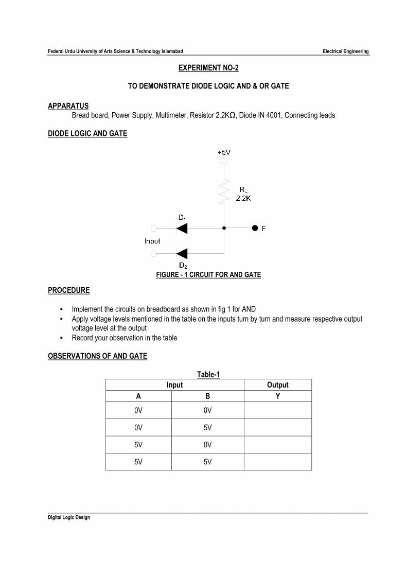
EXPERIMENT NO-2
TO DEMONSTRATE DIODE LOGIC AND & OR GATE
APPARATUS Bread board, Power Supply, Multimeter, Resistor 2.2KΩ, Diode IN 4001, Connecting leads DIODE LOGIC AND GATE
FIGURE - 1 CIRCUIT FOR AND GATE
PROCEDURE
• Implement the circuits on breadboard as shown in fig 1 for AND
• Apply voltage levels mentioned in the table on the inputs turn by turn and measure respective output voltage level at the output
• Record your observation in the table OBSERVATIONS OF AND GATE
Table-1
Input Output
A B Y
0V 0V 0V 5V 5V 0V 5V 5V
Federal Urdu University of Arts Science & Technology Islamabad Electrical Engineering
________________________________________________________________________________________________ Digital Logic Design
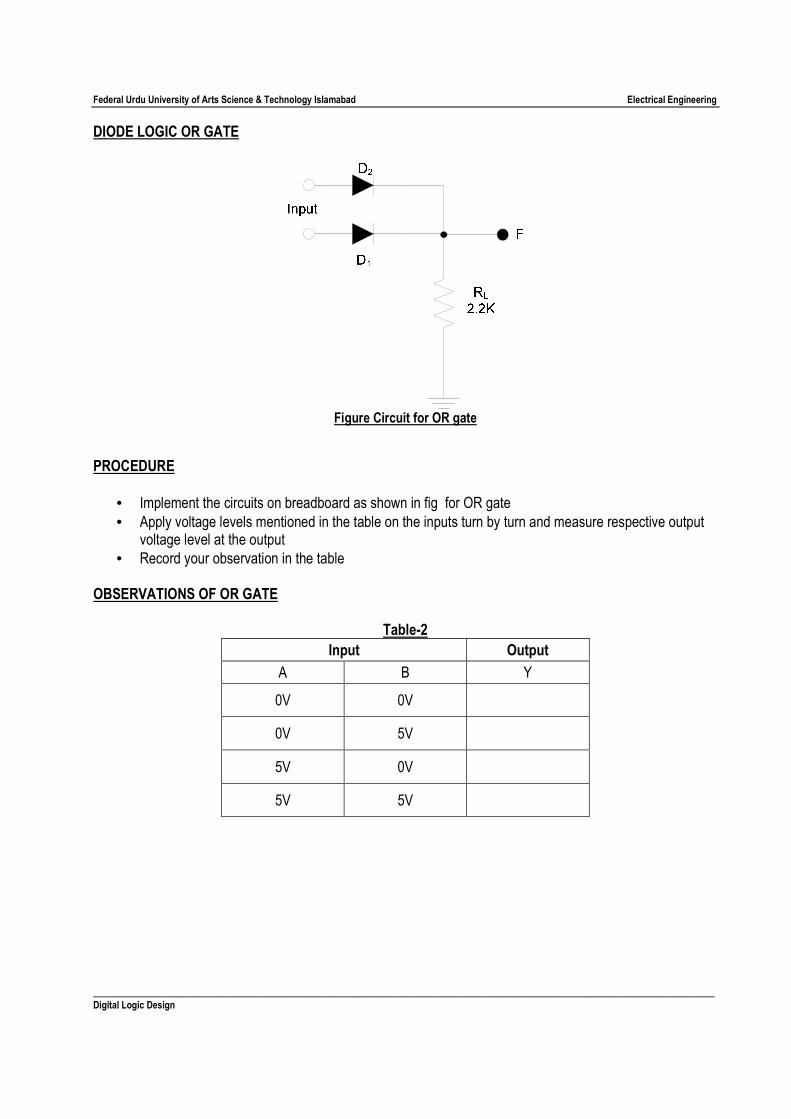
DIODE LOGIC OR GATE
Figure Circuit for OR gate
PROCEDURE
• Implement the circuits on breadboard as shown in fig for OR gate
• Apply voltage levels mentioned in the table on the inputs turn by turn and measure respective output voltage level at the output
• Record your observation in the table OBSERVATIONS OF OR GATE
Table-2
Input Output
A B Y
0V 0V 0V 5V 5V 0V 5V 5V
Federal Urdu University of Arts Science & Technology Islamabad Electrical Engineering
________________________________________________________________________________________________ Digital Logic Design
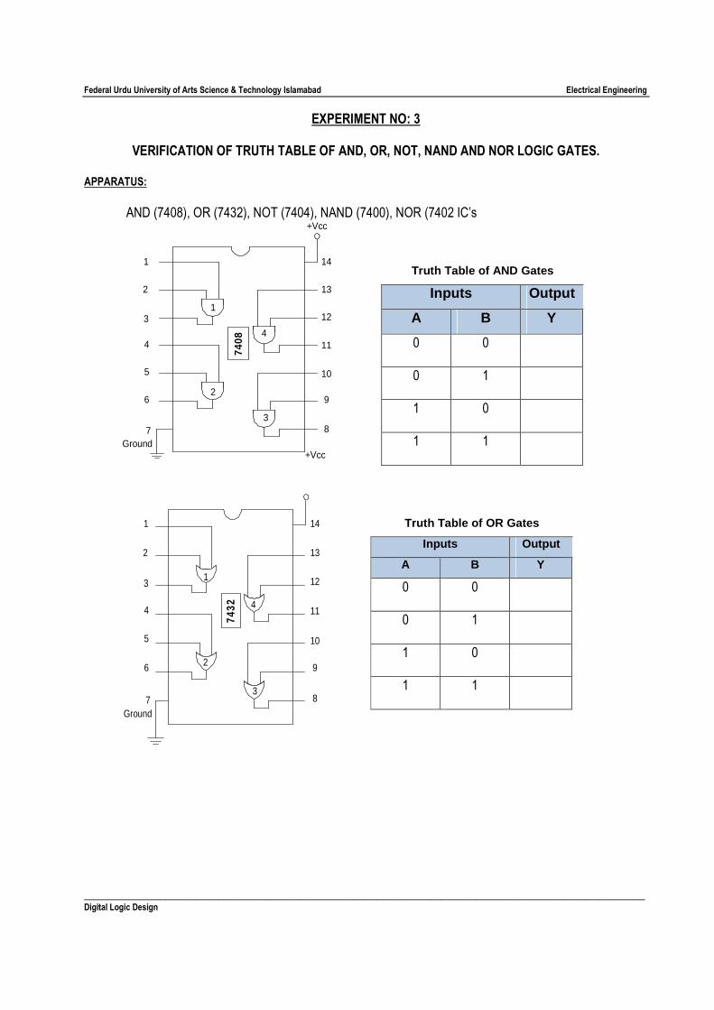
EXPERIMENT NO: 3
VERIFICATION OF TRUTH TABLE OF AND, OR, NOT, NAND AND NOR LOGIC GATES. APPARATUS:
AND (7408), OR (7432), NOT (7404), NAND (7400), NOR (7402 IC’s +Vcc
1
2
3
4
5
6
Ground
8
9
10
11
12
13
14
7
1
2
3
4
+Vcc
7408
1
2
3
4
5
6
Ground
8
9
10
11
12
13
14
7
1
2
3
4
7432
Truth Table of AND Gates
Inputs Output
A B Y
0 0
0 1
1 0
1 1
Truth Table of OR Gates
Inputs Output
A B Y
0 0
0 1
1 0
1 1
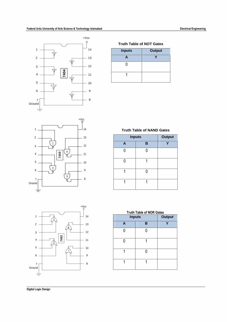
Federal Urdu University of Arts Science & Technology Islamabad Electrical Engineering
________________________________________________________________________________________________ Digital Logic Design
+Vcc
1
2
3
4
5
6
Ground8
9
10
11
12
13
14
7
1
2
3
4
5
6
7404
1
2
3
+Vcc
4
1
2
3
4
5
6
Ground
8
9
10
11
12
13
14
7
7400
7402
+Vcc
1
2
3
4
5
6
Ground
8
9
10
11
12
13
14
7
3
1
4
2
Truth Table of NOT Gates
Inputs Output
A Y
0
1
Truth Table of NAND Gates
Inputs Output
A B Y
0 0
0 1
1 0
1 1
Truth Table of NOR Gates
Inputs Output
A B Y
0 0
0 1
1 0
1 1
Federal Urdu University of Arts Science & Technology Islamabad Electrical Engineering
________________________________________________________________________________________________ Digital Logic Design
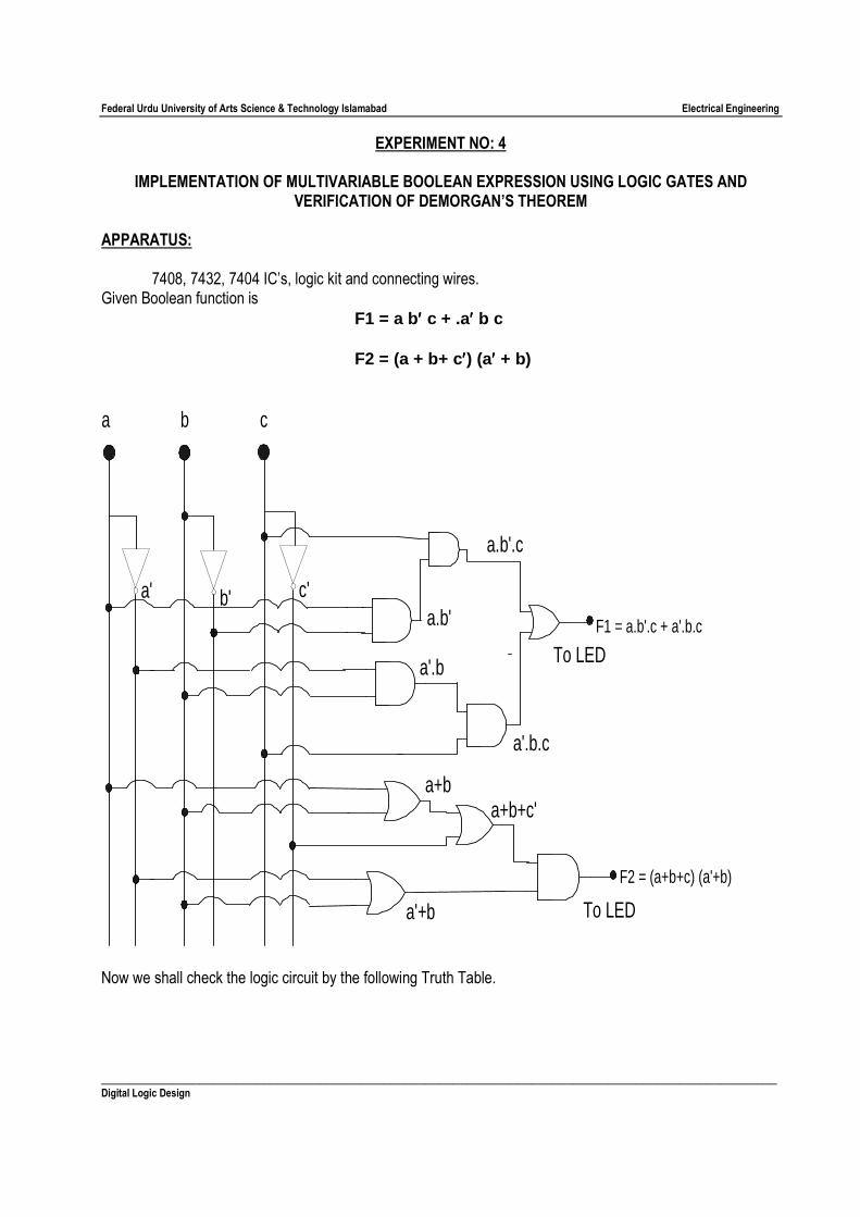
EXPERIMENT NO: 4
IMPLEMENTATION OF MULTIVARIABLE BOOLEAN EXPRESSION USING LOGIC GATES AND VERIFICATION OF DEMORGAN’S THEOREM
APPARATUS:
7408, 7432, 7404 IC’s, logic kit and connecting wires. Given Boolean function is
F1 = a b′′′′ c + .a′′′′ b c F2 = (a + b+ c ′′′′) (a′′′′ + b)
a
a'
b c
a.b'
a'.b
F1 = a.b'.c + a'.b.c
To LED
a'.b.c
a.b'.c
a+ba+b+c'
a'+b
F2 = (a+b+c) (a'+b)
To LED
b' c'
Now we shall check the logic circuit by the following Truth Table.

Federal Urdu University of Arts Science & Technology Islamabad Electrical Engineering
________________________________________________________________________________________________ Digital Logic Design
TRUTH TABLE
Inputs
Outputs F1 F2
a b c Actual Observed Actual Observed
0 0 0 0 0 1 0 1 0 0 1 1 1 0 0 1 0 1 1 1 0 1 1 1
Comments: __________________________________________________________________________ ____________________________________________________________________________________ ____________________________________________________________________________________ ____________________________________________________________________________________ ____________________________________________________________________________________ ____________________________________________________________________________________
Federal Urdu University of Arts Science & Technology Islamabad Electrical Engineering
________________________________________________________________________________________________ Digital Logic Design
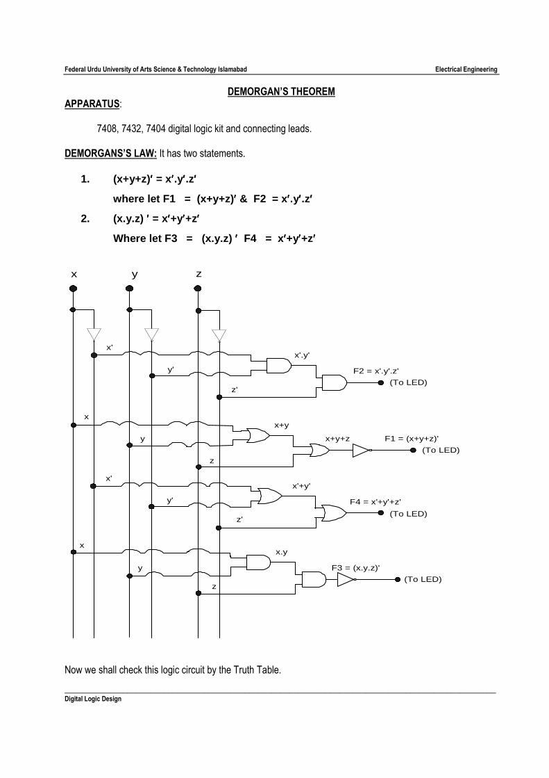
DEMORGAN’S THEOREM APPARATUS:
7408, 7432, 7404 digital logic kit and connecting leads. DEMORGANS’S LAW: It has two statements.
1. (x+y+z) ′′′′ = x ′′′′.y′′′′.z′′′′
where let F1 = (x+y+z) ′′′′ & F2 = x ′′′′.y′′′′.z′′′′
2. (x.y.z) ′′′′ = x′′′′+y′′′′+z′′′′
Where let F3 = (x.y.z) ′′′′ F4 = x ′′′′+y′′′′+z′′′′
(To LED)
x'.y'
F2 = x'.y'.z'
x+y
x+y+z
z'
F1 = (x+y+z)'
(To LED)
x'
y'
x
y
z
x'+y'
F4 = x'+y'+z'
(To LED)
x'
y'
x.y
F3 = (x.y.z)'
z(To LED)
x
y
z'
x y z
Now we shall check this logic circuit by the Truth Table.
Federal Urdu University of Arts Science & Technology Islamabad Electrical Engineering
________________________________________________________________________________________________ Digital Logic Design
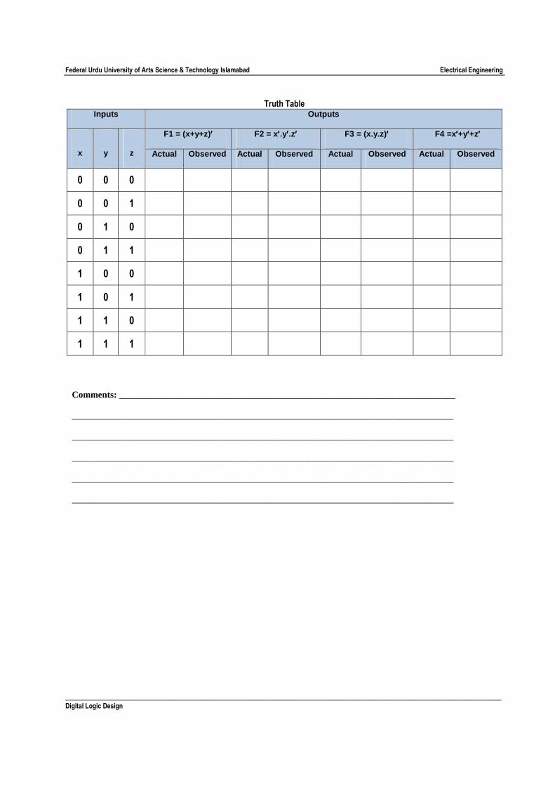
Truth Table
Inputs Outputs
x
y
z
F1 = (x+y+z) ′′′′ F2 = x ′′′′.y′′′′.z′′′′ F3 = (x.y.z) ′′′′ F4 =x′′′′+y′′′′+z′′′′
Actual Observed Actual Observed Actual Observed Actual Observed
0 0 0 0 0 1 0 1 0 0 1 1 1 0 0 1 0 1 1 1 0 1 1 1
Comments: __________________________________________________________________________ ____________________________________________________________________________________ ____________________________________________________________________________________ ____________________________________________________________________________________ ____________________________________________________________________________________ ____________________________________________________________________________________
Federal Urdu University of Arts Science & Technology Islamabad Electrical Engineering
________________________________________________________________________________________________ Digital Logic Design
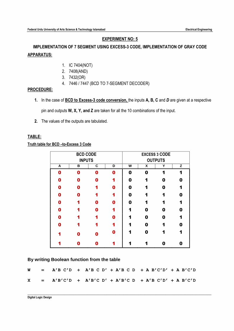
EXPERIMENT NO: 5
IMPLEMENTATION OF 7 SEGMENT USING EXCESS-3 CODE, IMPLEMENTATION OF GRAY CODE
APPARATUS:
1. IC 7404(NOT)
2. 7408(AND)
3. 7432(OR)
4. 7446 / 7447 (BCD TO 7-SEGMENT DECODER)
PROCEDURE:
1. In the case of BCD to Excess-3 code conversion, the inputs A, B, C and D are given at a respective
pin and outputs W, X, Y, and Z are taken for all the 10 combinations of the input.
2. The values of the outputs are tabulated.
TABLE:
Truth table for BCD –to-Excess 3 Code
BCD CODE
INPUTS
EXCESS 3 CODE
OUTPUTS A B C D W X Y Z
0 0 0 0 0 0 1 1
0 0 0 1 0 1 0 0
0 0 1 0 0 1 0 1
0 0 1 1 0 1 1 0
0 1 0 0 0 1 1 1
0 1 0 1 1 0 0 0
0 1 1 0 1 0 0 1
0 1 1 1 1 0 1 0
1 0 0 0 1 0 1 1
1 0 0 1 1 1 0 0
By writing Boolean function from the table
W = A’B C’D + A’B C D’ + A’B C D + A B’C’D’ + A B’C’D
X = A’B’C’D + A’B’C D’ + A’B’C D + A’B C’D’ + A B’C’D
Federal Urdu University of Arts Science & Technology Islamabad Electrical Engineering
________________________________________________________________________________________________ Digital Logic Design
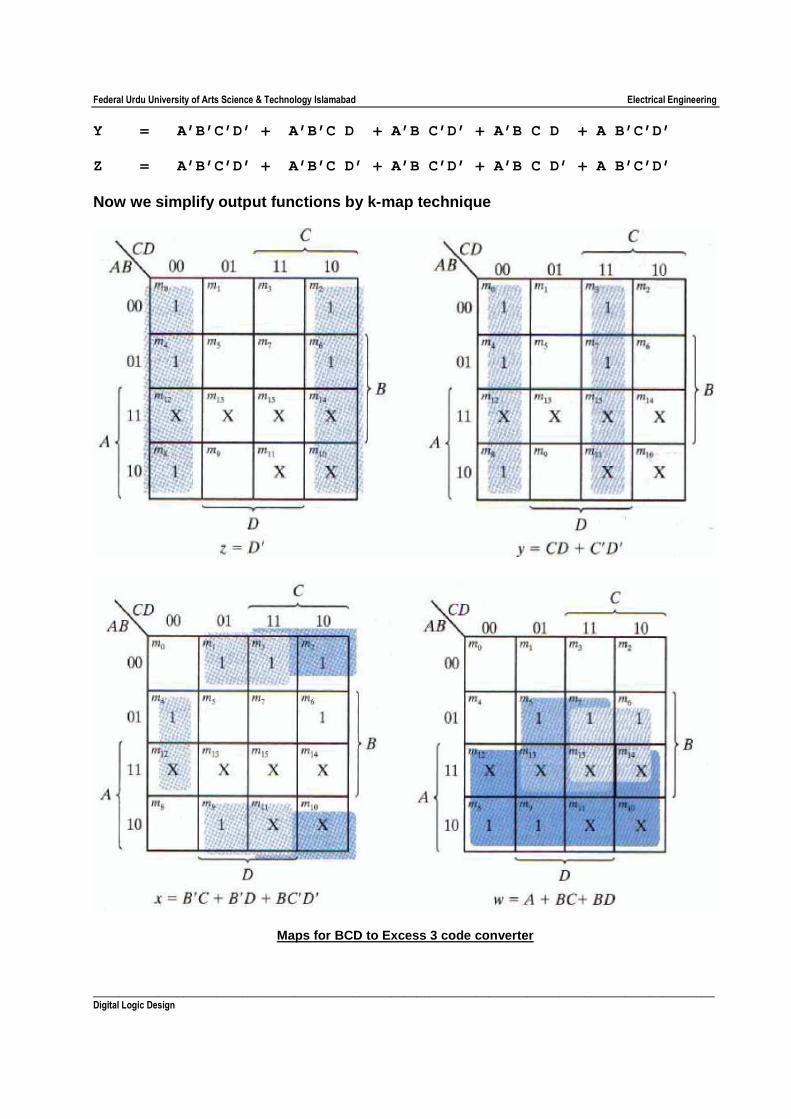
Y = A’B’C’D’ + A’B’C D + A’B C’D’ + A’B C D + A B’C’D’
Z = A’B’C’D’ + A’B’C D’ + A’B C’D’ + A’B C D’ + A B’C’D’
Now we simplify output functions by k-map technique
Maps for BCD to Excess 3 code converter
Federal Urdu University of Arts Science & Technology Islamabad Electrical Engineering
________________________________________________________________________________________________ Digital Logic Design
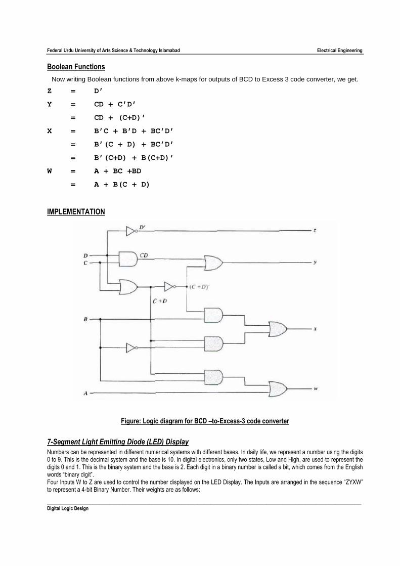
Boolean Functions
Now writing Boolean functions from above k-maps for outputs of BCD to Excess 3 code converter, we get.
Z = D’
Y = CD + C’D’
= CD + (C+D)’
X = B’C + B’D + BC’D’
= B’(C + D) + BC’D’
= B’(C+D) + B(C+D)’
W = A + BC +BD
= A + B(C + D)
IMPLEMENTATION
Figure: Logic diagram for BCD –to-Excess-3 code converter
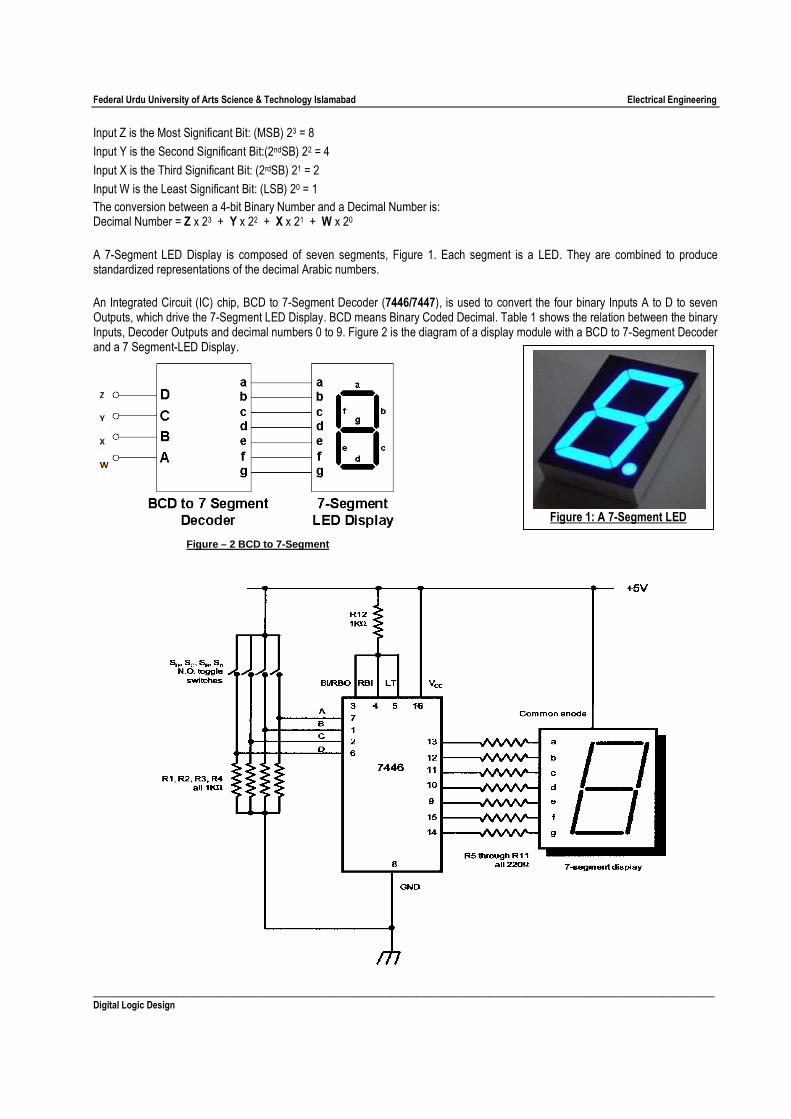
7-Segment Light Emitting Diode (LED) Display
Numbers can be represented in different numerical systems with different bases. In daily life, we represent a number using the digits 0 to 9. This is the decimal system and the base is 10. In digital electronics, only two states, Low and High, are used to represent the digits 0 and 1. This is the binary system and the base is 2. Each digit in a binary number is called a bit, which comes from the English words “binary digit”. Four Inputs W to Z are used to control the number displayed on the LED Display. The Inputs are arranged in the sequence “ZYXW” to represent a 4-bit Binary Number. Their weights are as follows:
Federal Urdu University of Arts Science & Technology Islamabad Electrical Engineering
________________________________________________________________________________________________ Digital Logic Design
Input Z is the Most Significant Bit: (MSB) 23 = 8
Input Y is the Second Significant Bit:(2ndSB) 22 = 4
Input X is the Third Significant Bit: (2rdSB) 21 = 2
Input W is the Least Significant Bit: (LSB) 20 = 1
The conversion between a 4-bit Binary Number and a Decimal Number is: Decimal Number = Z x 23 + Y x 22 + X x 21 + W x 20
A 7-Segment LED Display is composed of seven segments, Figure 1. Each segment is a LED. They are combined to produce standardized representations of the decimal Arabic numbers.
An Integrated Circuit (IC) chip, BCD to 7-Segment Decoder (7446/7447), is used to convert the four binary Inputs A to D to seven Outputs, which drive the 7-Segment LED Display. BCD means Binary Coded Decimal. Table 1 shows the relation between the binary Inputs, Decoder Outputs and decimal numbers 0 to 9. Figure 2 is the diagram of a display module with a BCD to 7-Segment Decoder and a 7 Segment-LED Display.
Figure – 2 BCD to 7-Segment
Figure 1: A 7-Segment LED
Display
Federal Urdu University of Arts Science & Technology Islamabad Electrical Engineering
________________________________________________________________________________________________ Digital Logic Design
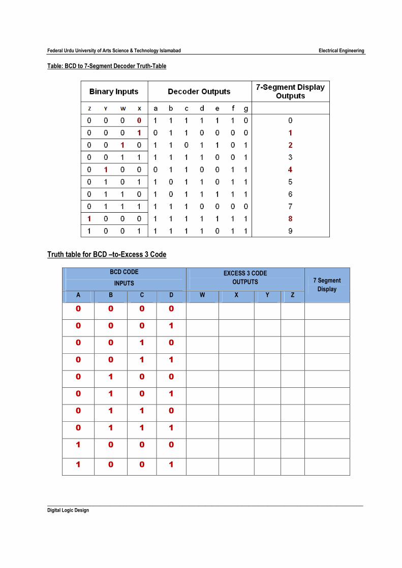
Table: BCD to 7-Segment Decoder Truth-Table
Truth table for BCD –to-Excess 3 Code
BCD CODE
INPUTS
EXCESS 3 CODE
OUTPUTS 7 Segment
Display A B C D W X Y Z
0 0 0 0
0 0 0 1
0 0 1 0
0 0 1 1
0 1 0 0
0 1 0 1
0 1 1 0
0 1 1 1
1 0 0 0
1 0 0 1
Federal Urdu University of Arts Science & Technology Islamabad Electrical Engineering
________________________________________________________________________________________________ Digital Logic Design
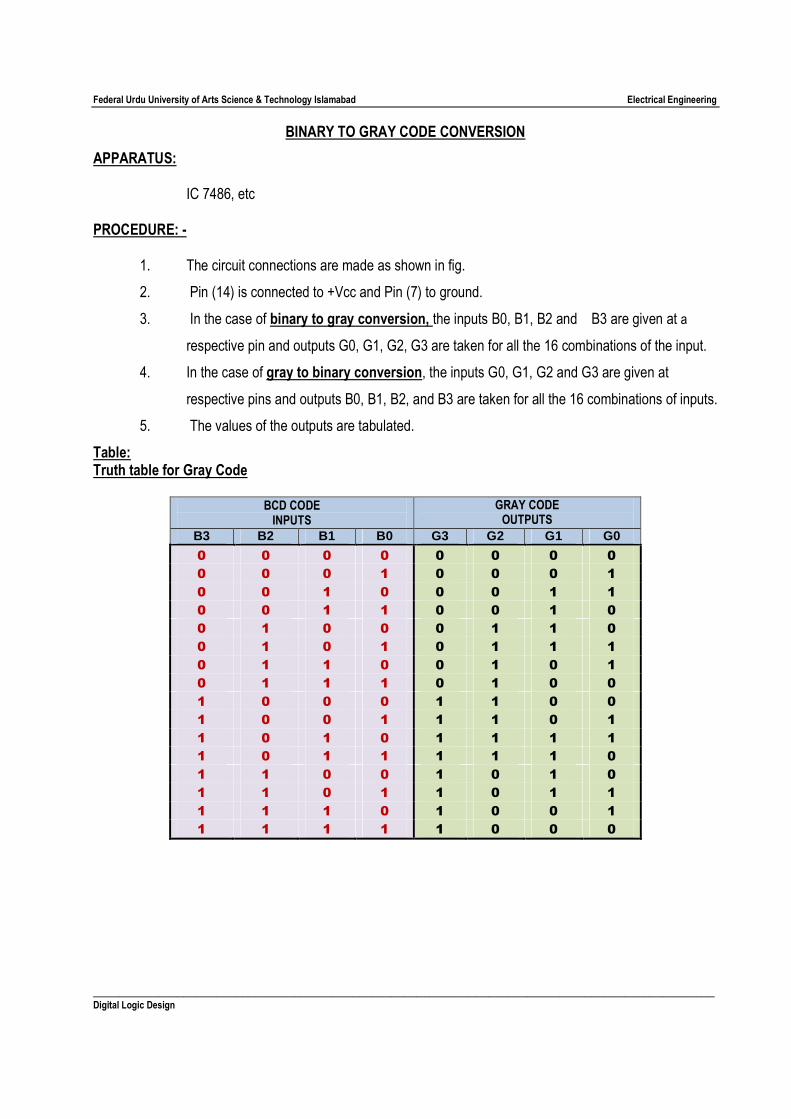
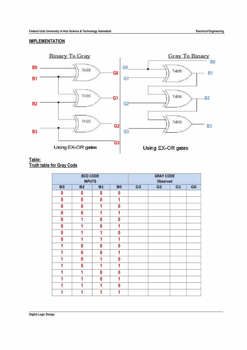
BINARY TO GRAY CODE CONVERSION
APPARATUS:
IC 7486, etc
PROCEDURE: -
1. The circuit connections are made as shown in fig.
2. Pin (14) is connected to +Vcc and Pin (7) to ground.
3. In the case of binary to gray conversion, the inputs B0, B1, B2 and B3 are given at a
respective pin and outputs G0, G1, G2, G3 are taken for all the 16 combinations of the input.
4. In the case of gray to binary conversion, the inputs G0, G1, G2 and G3 are given at
respective pins and outputs B0, B1, B2, and B3 are taken for all the 16 combinations of inputs.
5. The values of the outputs are tabulated.
Table: Truth table for Gray Code
BCD CODE INPUTS
GRAY CODE OUTPUTS
B3 B2 B1 B0 G3 G2 G1 G0
0 0 0 0 0 0 0 0
0 0 0 1 0 0 0 1
0 0 1 0 0 0 1 1
0 0 1 1 0 0 1 0
0 1 0 0 0 1 1 0
0 1 0 1 0 1 1 1
0 1 1 0 0 1 0 1
0 1 1 1 0 1 0 0
1 0 0 0 1 1 0 0
1 0 0 1 1 1 0 1
1 0 1 0 1 1 1 1
1 0 1 1 1 1 1 0
1 1 0 0 1 0 1 0
1 1 0 1 1 0 1 1
1 1 1 0 1 0 0 1
1 1 1 1 1 0 0 0
Federal Urdu University of Arts Science & Technology Islamabad Electrical Engineering
________________________________________________________________________________________________ Digital Logic Design
IMPLEMENTATION
Table: Truth table for Gray Code
BCD CODE
INPUTS
GRAY CODE
Observed
B3 B2 B1 B0 G3 G2 G1 G0
0 0 0 0
0 0 0 1
0 0 1 0
0 0 1 1
0 1 0 0
0 1 0 1
0 1 1 0
0 1 1 1
1 0 0 0
1 0 0 1
1 0 1 0
1 0 1 1
1 1 0 0
1 1 0 1
1 1 1 0
1 1 1 1
B0 B0 G0 G0 B1 B1 G1
G1 B2 B2 G2 G2 B3 B3 G3 G3
Federal Urdu University of Arts Science & Technology Islamabad Electrical Engineering
________________________________________________________________________________________________ Digital Logic Design
EXPERIMENT NO: 6 IMPLEMENTATION OF HALF ADDER & FULL ADDER
APPARATUS:
7486, 7432, 7408, 7404 IC’s, logic kit and connecting leads.
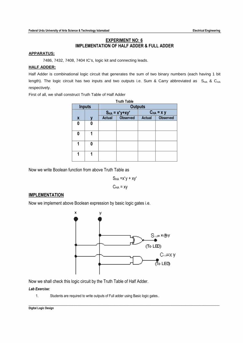
HALF ADDER:
Half Adder is combinational logic circuit that generates the sum of two binary numbers (each having 1 bit
length). The logic circuit has two inputs and two outputs i.e. Sum & Carry abbreviated as SHA & CHA
respectively.
First of all, we shall construct Truth Table of Half Adder
Truth Table
Inputs Outputs
x
y
SHA = x′′′′y+xy′′′′ CHA = x y Actual Observed Actual Observed
0 0 0 1 1 0 1 1
Now we write Boolean function from above Truth Table as
SHA =x′y + xy′
CHA = xy
IMPLEMENTATION
Now we implement above Boolean expression by basic logic gates i.e.
Now we shall check this logic circuit by the Truth Table of Half Adder.
Lab Exercise:
1. Students are required to write outputs of Full adder using Basic logic gates..
Federal Urdu University of Arts Science & Technology Islamabad Electrical Engineering
________________________________________________________________________________________________ Digital Logic Design
2. Then implement Half Adder using basic logic gates.
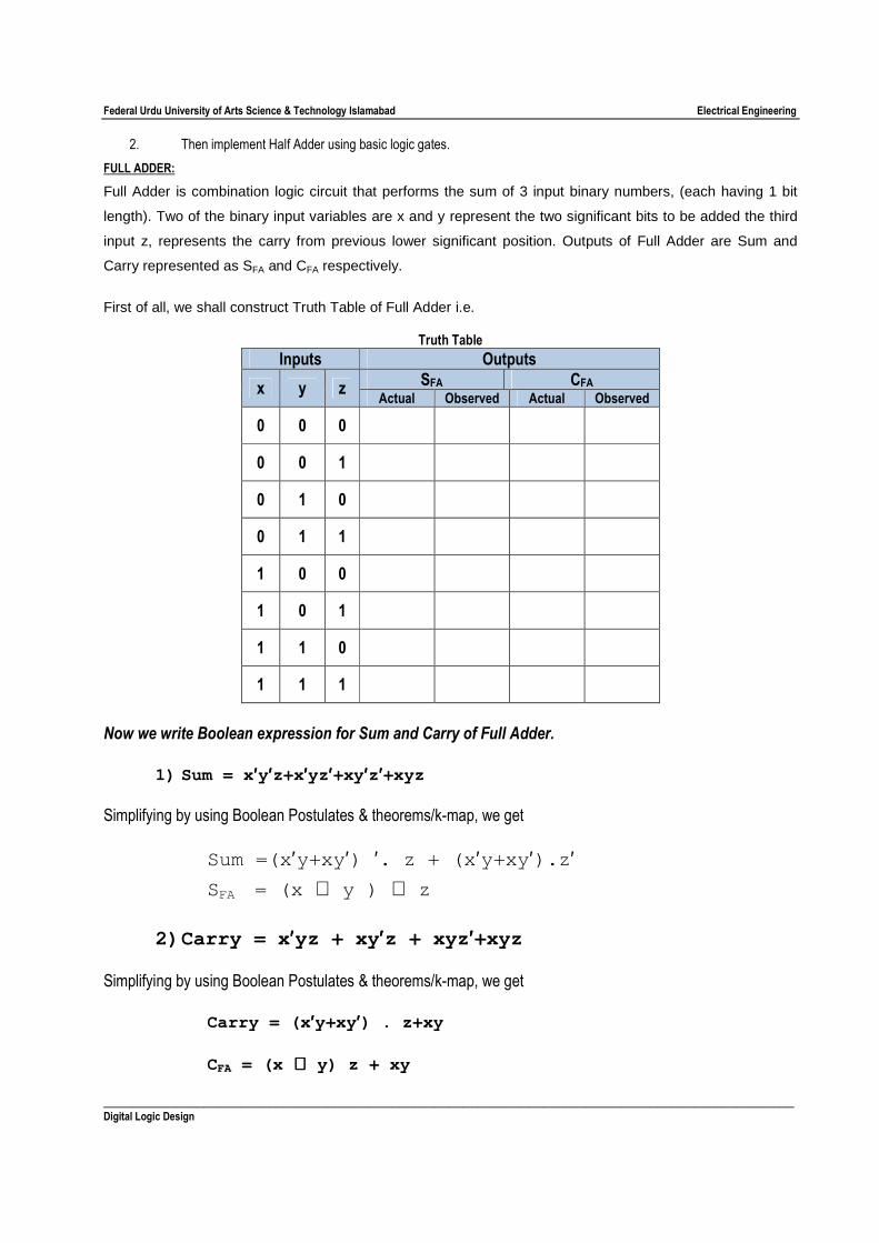
FULL ADDER:
Full Adder is combination logic circuit that performs the sum of 3 input binary numbers, (each having 1 bit
length). Two of the binary input variables are x and y represent the two significant bits to be added the third
input z, represents the carry from previous lower significant position. Outputs of Full Adder are Sum and
Carry represented as SFA and CFA respectively.
First of all, we shall construct Truth Table of Full Adder i.e.
Truth Table
Inputs Outputs
x y z SFA CFA
Actual Observed Actual Observed
0 0 0 0 0 1 0 1 0 0 1 1 1 0 0 1 0 1 1 1 0 1 1 1
Now we write Boolean expression for Sum and Carry of Full Adder.
1) Sum = x ′′′′y ′′′′z+x ′′′′yz ′′′′+xy ′′′′z ′′′′+xyz Simplifying by using Boolean Postulates & theorems/k-map, we get
Sum =(x′y+xy′) ′. z + (x′y+xy′).z′ SFA = (x ⊕ y ) ⊕ z
2) Carry = x ′′′′yz + xy ′′′′z + xyz ′′′′+xyz Simplifying by using Boolean Postulates & theorems/k-map, we get
Carry = (x ′′′′y+xy ′′′′) . z+xy
CFA = (x ⊕⊕⊕⊕ y) z + xy
Federal Urdu University of Arts Science & Technology Islamabad Electrical Engineering
________________________________________________________________________________________________ Digital Logic Design
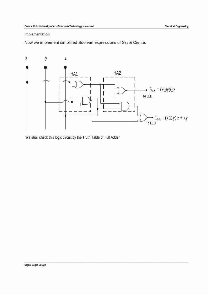
Implementation Now we implement simplified Boolean expressions of SFA & CFA i.e.
x y z
To LED
To LED
HA2HA1
SFA = (x y) z + +
CFA = (x y) z + xy +
We shall check this logic circuit by the Truth Table of Full Adder
Federal Urdu University of Arts Science & Technology Islamabad Electrical Engineering
________________________________________________________________________________________________ Digital Logic Design
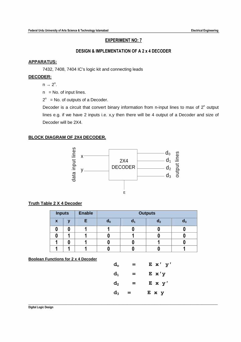
EXPERIMENT NO: 7
DESIGN & IMPLEMENTATION OF A 2 x 4 DECODER
APPARATUS:
7432, 7408, 7404 IC’s logic kit and connecting leads
DECODER:
n → 2n.
n = No. of input lines.
2n = No. of outputs of a Decoder.
Decoder is a circuit that convert binary information from n-input lines to max of 2n output
lines e.g. if we have 2 inputs i.e. x,y then there will be 4 output of a Decoder and size of
Decoder will be 2X4.
BLOCK DIAGRAM OF 2X4 DECODER.
d12X4DECODER d2
d3
d0
E
data
inpu
t lin
es
outp
ut li
nes
x
y
Truth Table 2 X 4 Decoder
Inputs Enable Outputs
x y E d0 d1 d2 d3
0 0 1 1 0 0 0
0 1 1 0 1 0 0
1 0 1 0 0 1 0
1 1 1 0 0 0 1 Boolean Functions for 2 x 4 Decoder
do = E x ′ y ′
d1 = E x ′y
d2 = E x y ′
d3 = E x y
Federal Urdu University of Arts Science & Technology Islamabad Electrical Engineering
________________________________________________________________________________________________ Digital Logic Design
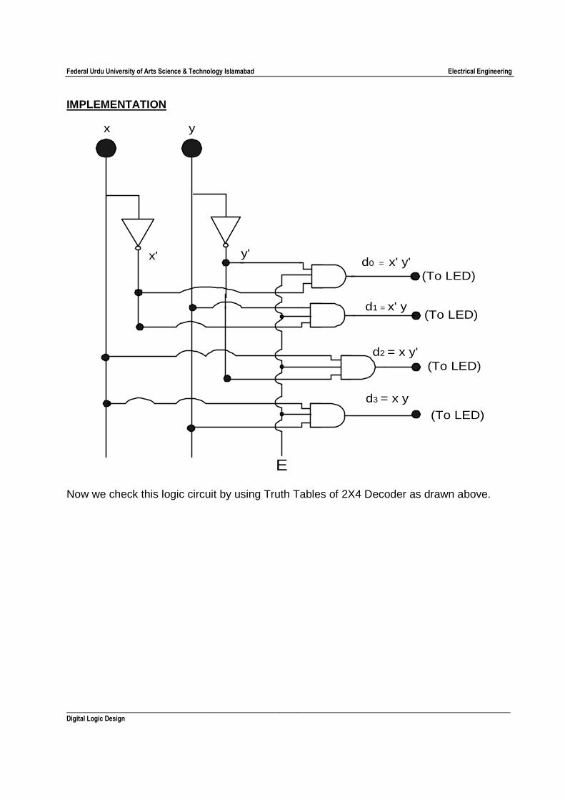
IMPLEMENTATION
d0 = x' y'
d1 = x' y
x
x'
y
(To LED)
y'
(To LED)
d2 = x y'(To LED)
(To LED)
d3 = x y
E
Now we check this logic circuit by using Truth Tables of 2X4 Decoder as drawn above.
Federal Urdu University of Arts Science & Technology Islamabad Electrical Engineering
________________________________________________________________________________________________ Digital Logic Design
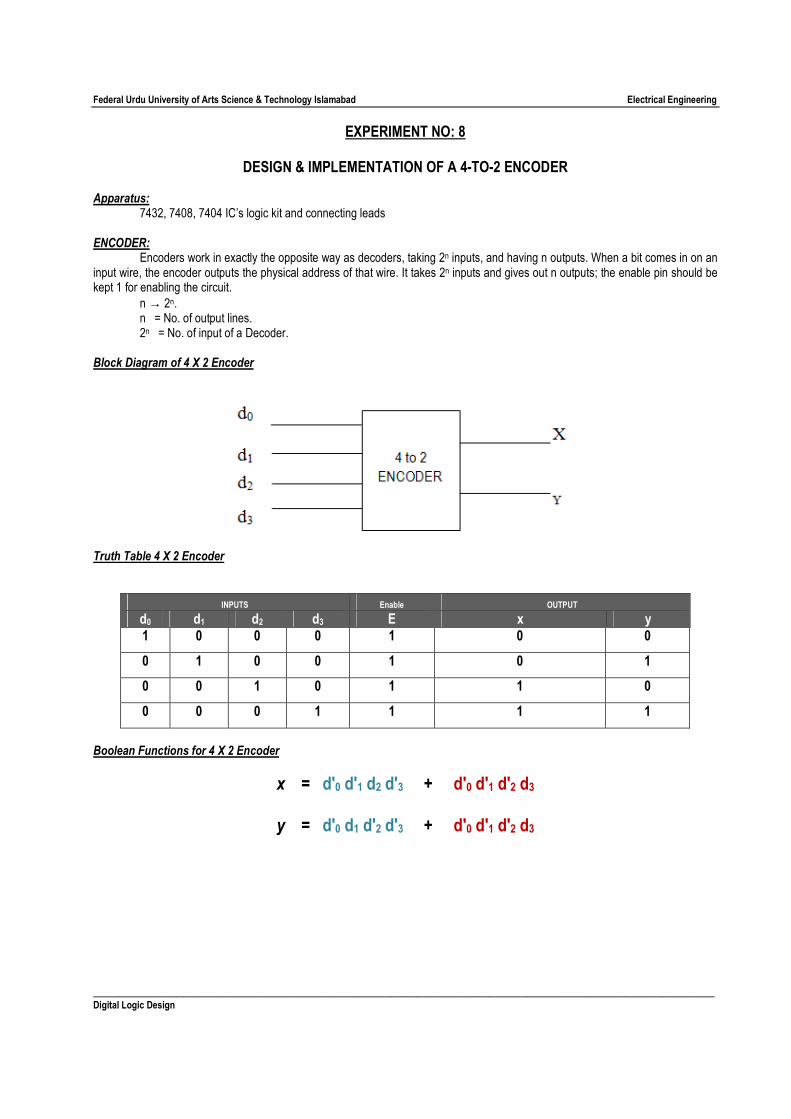
EXPERIMENT NO: 8
DESIGN & IMPLEMENTATION OF A 4-TO-2 ENCODER
Apparatus: 7432, 7408, 7404 IC’s logic kit and connecting leads
ENCODER:
Encoders work in exactly the opposite way as decoders, taking 2n inputs, and having n outputs. When a bit comes in on an input wire, the encoder outputs the physical address of that wire. It takes 2n inputs and gives out n outputs; the enable pin should be kept 1 for enabling the circuit.
n → 2n. n = No. of output lines. 2n = No. of input of a Decoder. Block Diagram of 4 X 2 Encoder
Truth Table 4 X 2 Encoder
INPUTS Enable OUTPUT
d0 d1 d2 d3 E x y
1 0 0 0 1 0 0
0 1 0 0 1 0 1
0 0 1 0 1 1 0
0 0 0 1 1 1 1
Boolean Functions for 4 X 2 Encoder
x = d′0 d′1 d2 d′3 + d′0 d′1 d′2 d3
y = d′0 d1 d′2 d′3 + d′0 d′1 d′2 d3
Federal Urdu University of Arts Science & Technology Islamabad Electrical Engineering
________________________________________________________________________________________________ Digital Logic Design
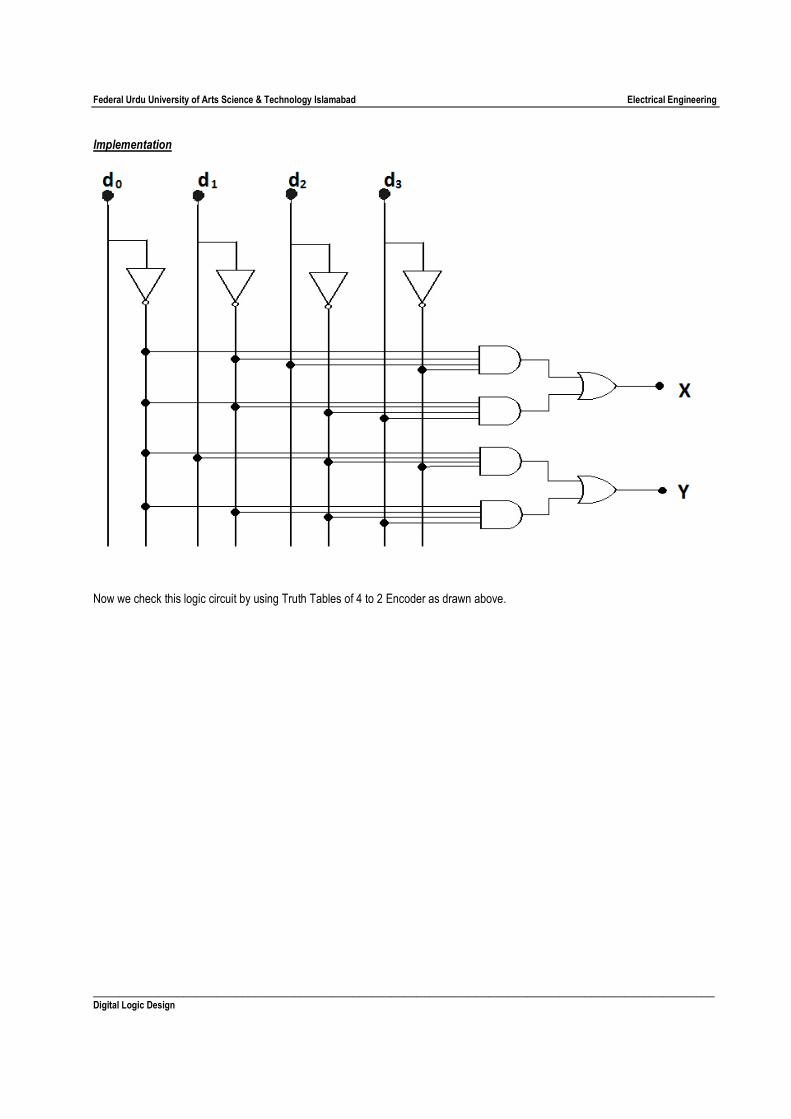
Implementation
Now we check this logic circuit by using Truth Tables of 4 to 2 Encoder as drawn above.
Federal Urdu University of Arts Science & Technology Islamabad Electrical Engineering
________________________________________________________________________________________________ Digital Logic Design
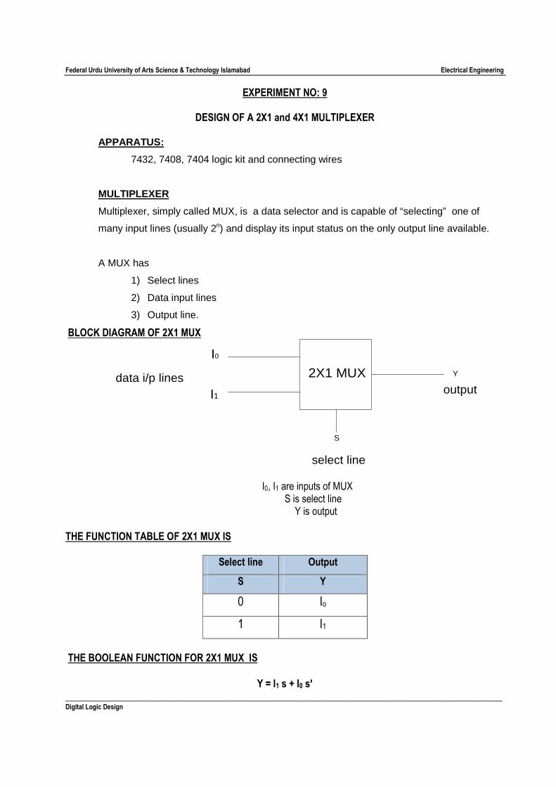
EXPERIMENT NO: 9
DESIGN OF A 2X1 and 4X1 MULTIPLEXER
APPARATUS:
7432, 7408, 7404 logic kit and connecting wires
MULTIPLEXER
Multiplexer, simply called MUX, is a data selector and is capable of “selecting” one of
many input lines (usually 2n) and display its input status on the only output line available.
A MUX has
1) Select lines
2) Data input lines
3) Output line.
BLOCK DIAGRAM OF 2X1 MUX
data i/p lines
select line
output
I0
I1
S
Y2X1 MUX
I0, I1 are inputs of MUX
S is select line Y is output
THE FUNCTION TABLE OF 2X1 MUX IS
Select line Output
S Y
0 Io
1 I1
THE BOOLEAN FUNCTION FOR 2X1 MUX IS
Y = I1 s + I0 s′′′′
Federal Urdu University of Arts Science & Technology Islamabad Electrical Engineering
________________________________________________________________________________________________ Digital Logic Design
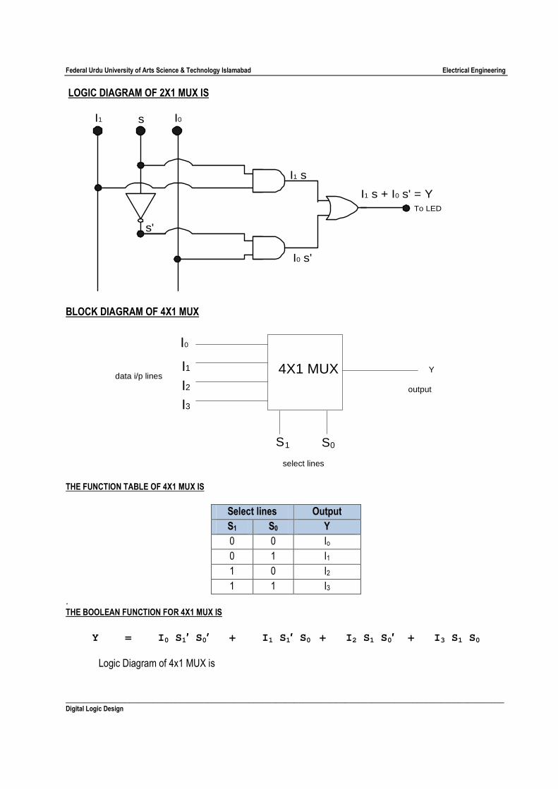
LOGIC DIAGRAM OF 2X1 MUX IS
I1 I0s
I1 s
I0 s'
s'
I1 s + I0 s' = YTo LED
BLOCK DIAGRAM OF 4X1 MUX
I0
I1
S1
Y4X1 MUXI2I3
S0
data i/p lines
select lines
output
THE FUNCTION TABLE OF 4X1 MUX IS
Select lines Output
S1 S0 Y
0 0 Io
0 1 I1
1 0 I2
1 1 I3
. THE BOOLEAN FUNCTION FOR 4X1 MUX IS
Y = I 0 S 1′′′′ S 0′′′′ + I 1 S 1′′′′ S 0 + I 2 S 1 S 0′′′′ + I 3 S 1 S 0
Logic Diagram of 4x1 MUX is
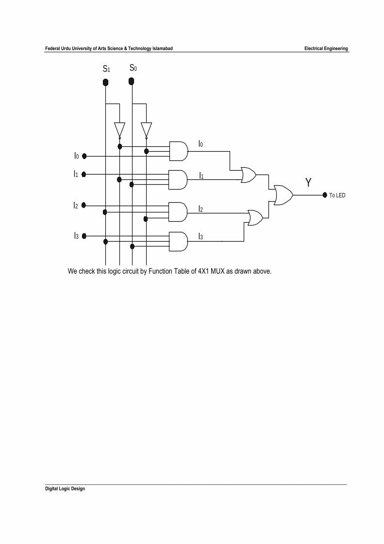
Federal Urdu University of Arts Science & Technology Islamabad Electrical Engineering
________________________________________________________________________________________________ Digital Logic Design
To LED
S1 S0
I0
I1
I2
I3
I0
I1
I2
I3
Y
We check this logic circuit by Function Table of 4X1 MUX as drawn above.
Federal Urdu University of Arts Science & Technology Islamabad Electrical Engineering
________________________________________________________________________________________________ Digital Logic Design
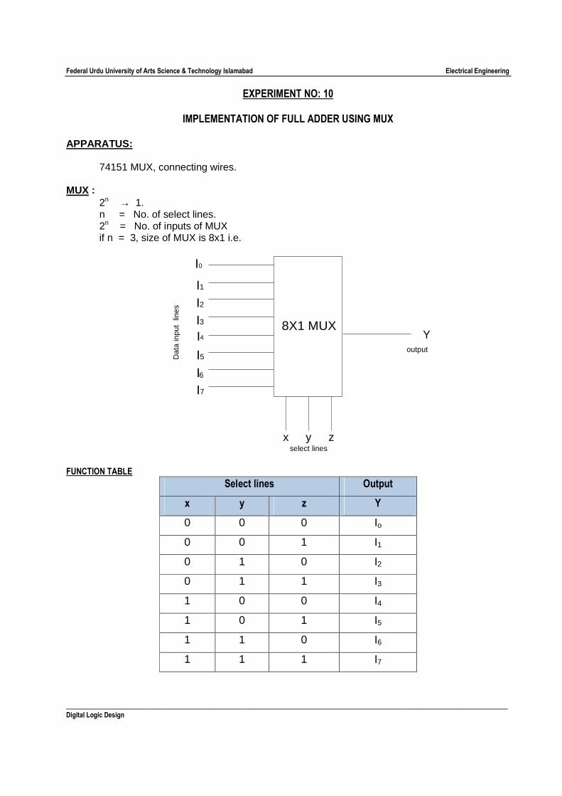
EXPERIMENT NO: 10
IMPLEMENTATION OF FULL ADDER USING MUX APPARATUS:
74151 MUX, connecting wires. MUX :
2n → 1. n = No. of select lines. 2n = No. of inputs of MUX if n = 3, size of MUX is 8x1 i.e.
I0
I1
x
Y8X1 MUX
I2I3
Dat
a in
put
lines
output
I4
I5
I6I7
y zselect lines
FUNCTION TABLE
Select lines Output
x y z Y
0 0 0 Io
0 0 1 I1
0 1 0 I2
0 1 1 I3
1 0 0 I4
1 0 1 I5
1 1 0 I6
1 1 1 I7
Federal Urdu University of Arts Science & Technology Islamabad Electrical Engineering
________________________________________________________________________________________________ Digital Logic Design
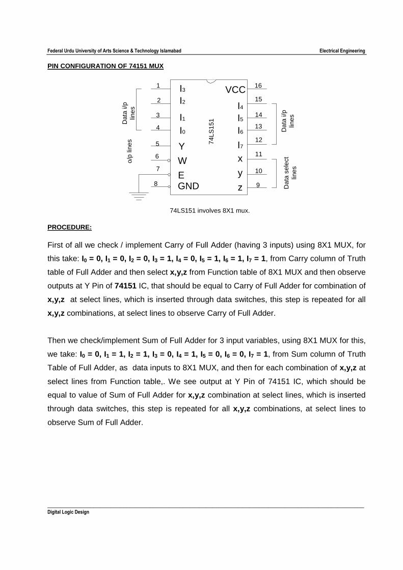
PIN CONFIGURATION OF 74151 MUX
I3
I2
I1
I0
Y
W
EGND
1
2
3
4
5
6
7
8
Dat
a i/p
lines
o/p
lines
9
10
11
12
13
14
15
16
Dat
a i/p
lines
Dat
a se
lect
lines
x
y
z
I7
I6
I5
I4
VCC
74LS
151
74LS151 involves 8X1 mux. PROCEDURE: First of all we check / implement Carry of Full Adder (having 3 inputs) using 8X1 MUX, for
this take: I0 = 0, I1 = 0, I2 = 0, I3 = 1, I4 = 0, I5 = 1, I6 = 1, I7 = 1, from Carry column of Truth
table of Full Adder and then select x,y,z from Function table of 8X1 MUX and then observe
outputs at Y Pin of 74151 IC, that should be equal to Carry of Full Adder for combination of
x,y,z at select lines, which is inserted through data switches, this step is repeated for all
x,y,z combinations, at select lines to observe Carry of Full Adder.
Then we check/implement Sum of Full Adder for 3 input variables, using 8X1 MUX for this,
we take: I0 = 0, I1 = 1, I2 = 1, I3 = 0, I4 = 1, I5 = 0, I6 = 0, I7 = 1, from Sum column of Truth
Table of Full Adder, as data inputs to 8X1 MUX, and then for each combination of x,y,z at
select lines from Function table,. We see output at Y Pin of 74151 IC, which should be
equal to value of Sum of Full Adder for x,y,z combination at select lines, which is inserted
through data switches, this step is repeated for all x,y,z combinations, at select lines to
observe Sum of Full Adder.
Federal Urdu University of Arts Science & Technology Islamabad Electrical Engineering
________________________________________________________________________________________________ Digital Logic Design
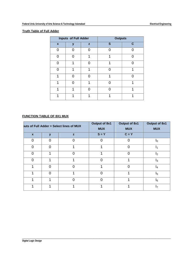
Truth Table of Full Adder
Inputs of Full Adder Outputs
x y z S C
0 0 0 0 0
0 0 1 1 0
0 1 0 1 0
0 1 1 0 1
1 0 0 1 0
1 0 1 0 1
1 1 0 0 1
1 1 1 1 1
FUNCTION TABLE OF 8X1 MUX
Inputs of Full Adder = Select lines of MUX Output of 8x1
MUX
Output of 8x1
MUX
Output of 8x1
MUX
x y z S = Y C = Y
0 0 0 0 0 I0
0 0 1 1 0 I1
0 1 0 1 0 I2
0 1 1 0 1 I3
1 0 0 1 0 I4
1 0 1 0 1 I5
1 1 0 0 1 I6
1 1 1 1 1 I7
Federal Urdu University of Arts Science & Technology Islamabad Electrical Engineering
________________________________________________________________________________________________ Digital Logic Design
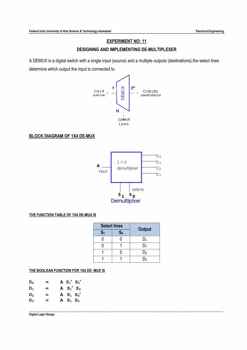
EXPERIMENT NO: 11
DESIGNING AND IMPLEMENTING DE-MULTIPLEXER
A DEMUX is a digital switch with a single input (source) and a multiple outputs (destinations).the select lines
determine which output the input is connected to.
BLOCK DIAGRAM OF 1X4 DE-MUX
THE FUNCTION TABLE OF 1X4 DE-MUX IS
Select lines Output
S1 S0
0 0 Do
0 1 D1
1 0 D2
1 1 D3
. THE BOOLEAN FUNCTION FOR 1X4 DE- MUX IS
D0 = A S 1′′′′ S 0′′′′ D1 = A S1′′′′ S 0
D2 = A S1 S 0′′′′ D3 = A S1 S 0
Federal Urdu University of Arts Science & Technology Islamabad Electrical Engineering
________________________________________________________________________________________________ Digital Logic Design
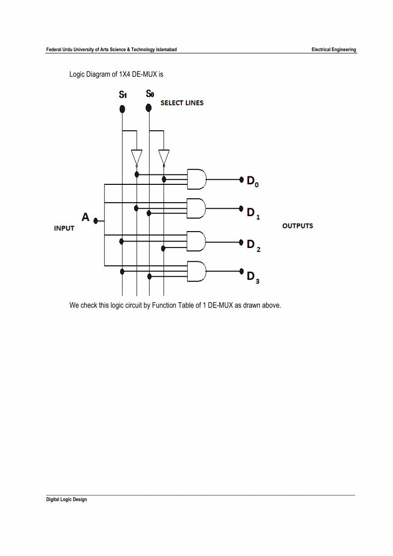
Logic Diagram of 1X4 DE-MUX is
We check this logic circuit by Function Table of 1 DE-MUX as drawn above.
Federal Urdu University of Arts Science & Technology Islamabad Electrical Engineering
________________________________________________________________________________________________ Digital Logic Design
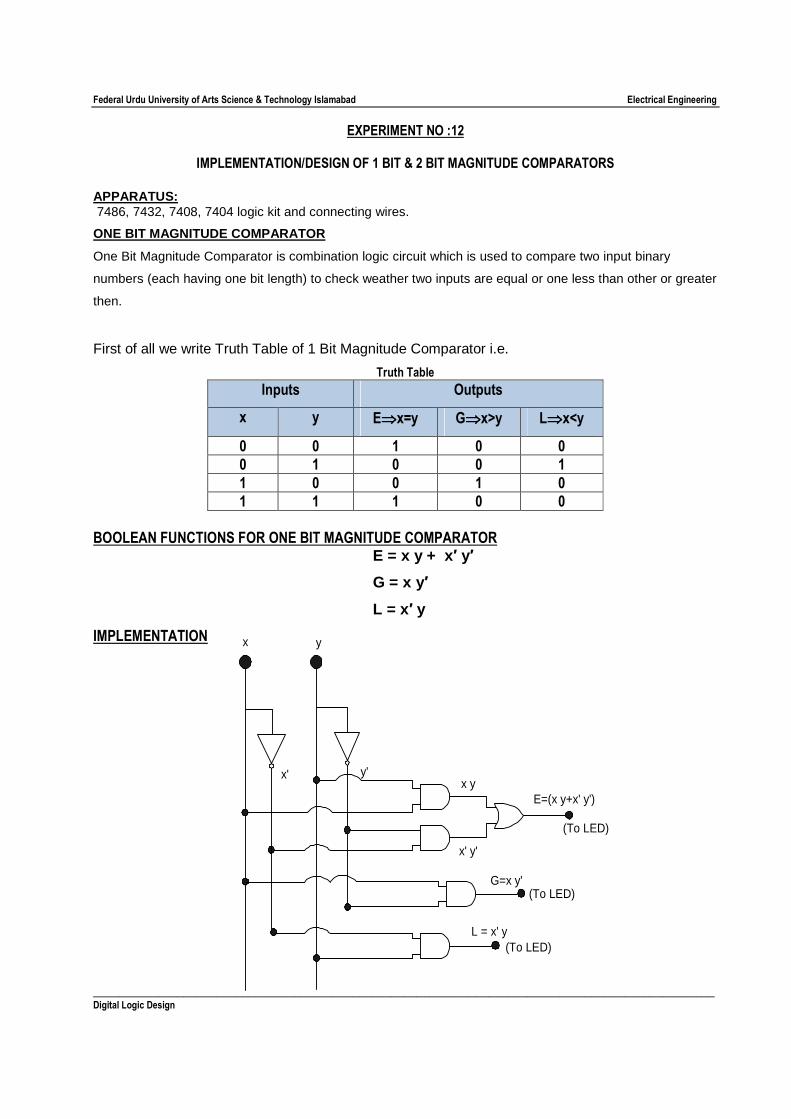
EXPERIMENT NO :12
IMPLEMENTATION/DESIGN OF 1 BIT & 2 BIT MAGNITUDE COMPARATORS
APPARATUS: 7486, 7432, 7408, 7404 logic kit and connecting wires.
ONE BIT MAGNITUDE COMPARATOR
One Bit Magnitude Comparator is combination logic circuit which is used to compare two input binary
numbers (each having one bit length) to check weather two inputs are equal or one less than other or greater
then.
First of all we write Truth Table of 1 Bit Magnitude Comparator i.e.
Truth Table
Inputs Outputs
x y E⇒⇒⇒⇒x=y G⇒⇒⇒⇒x>y L⇒⇒⇒⇒x<y
0 0 1 0 0
0 1 0 0 1
1 0 0 1 0
1 1 1 0 0
BOOLEAN FUNCTIONS FOR ONE BIT MAGNITUDE COMPARATOR
E = x y + x ′ y′
G = x y ′
L = x ′ y
IMPLEMENTATION
x y
x' y'
E=(x y+x' y')
x
x'
y
(To LED)
y'
L = x' y(To LED)
G=x y'(To LED)
Federal Urdu University of Arts Science & Technology Islamabad Electrical Engineering
________________________________________________________________________________________________ Digital Logic Design
To check this logic circuit, we shall use the above Truth Table
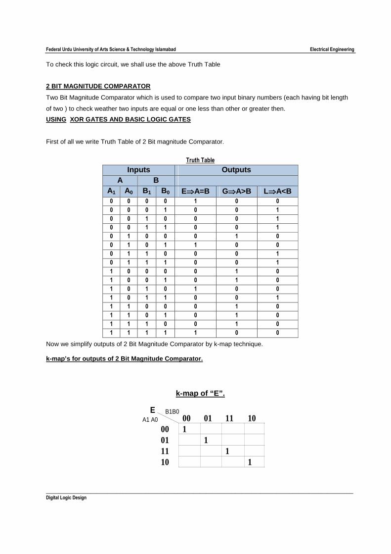
2 BIT MAGNITUDE COMPARATOR
Two Bit Magnitude Comparator which is used to compare two input binary numbers (each having bit length
of two ) to check weather two inputs are equal or one less than other or greater then.
USING XOR GATES AND BASIC LOGIC GATES
First of all we write Truth Table of 2 Bit magnitude Comparator.
Truth Table
Now we simplify outputs of 2 Bit Magnitude Comparator by k-map technique. k-map’s for outputs of 2 Bit Magnitude Comparator.
k-map of “E”.
00 01 11 1000 101 111 110 1
B1B0A1 A0
E
Inputs Outputs A B
A1 A0 B1 B0 E⇒⇒⇒⇒A=B G⇒⇒⇒⇒A>B L⇒⇒⇒⇒A<B 0 0 0 0 1 0 0
0 0 0 1 0 0 1
0 0 1 0 0 0 1
0 0 1 1 0 0 1
0 1 0 0 0 1 0
0 1 0 1 1 0 0
0 1 1 0 0 0 1
0 1 1 1 0 0 1
1 0 0 0 0 1 0
1 0 0 1 0 1 0
1 0 1 0 1 0 0
1 0 1 1 0 0 1
1 1 0 0 0 1 0
1 1 0 1 0 1 0
1 1 1 0 0 1 0
1 1 1 1 1 0 0

Federal Urdu University of Arts Science & Technology Islamabad Electrical Engineering
________________________________________________________________________________________________ Digital Logic Design
k-map of “G” B1B0
A1A0 00 01 11 100001 111 1 1 110 1 1
G
k-map of “L”.
B1B0A1 A0 00 01 11 10
00 1 1 1 01 1 1 11 10 1
L
BOOLEAN FUNCTIONS
Now writing Boolean functions from above k-maps for outputs of two Bit Magnitude Comparator, we get.
E = A′′′′1 A′′′′0 B′′′′1 B′′′′0+ A′′′′1 A0 B′′′′1 B0 + A1 A0 B1 B0+ A1 A′′′′0 B1 B′′′′0
E = A′1 B′1(A′0 B′0+ A0 B0) + A1 B1(A0 B0+ A′0 B′0)
E = (A′0 B′0+ A0 B0) (A′1 B′1+ A1 B1)
+(A1 B1)'+(A0 B0)'E =
G = A1B′′′′1 + A′′′′1 A0 B′′′′1 B′′′′0 + A1 A0 B1 B′′′′0
G = A1B′1 + A0 B′0 (A′1B′1 + A1 B1)
+(A1 B1)'G = A1B'1 + A0B'0
L = A ′′′′1B1 + A′′′′0 B0 (A′′′′1B′′′′1 + A1 B1)
+(A1 B1)'L = A'1B1 + A'0B0
Federal Urdu University of Arts Science & Technology Islamabad Electrical Engineering
________________________________________________________________________________________________ Digital Logic Design
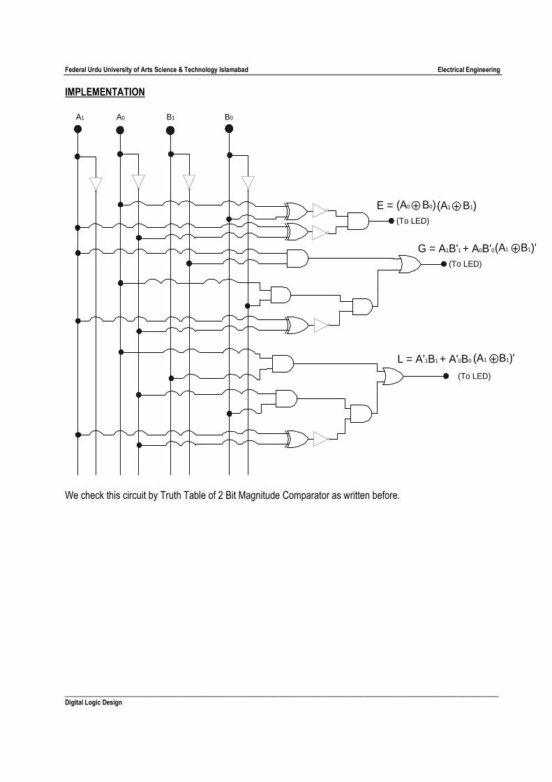
IMPLEMENTATION
(To LED)
A1 A0 B1 B0
(To LED)
(To LED)
+(A1 B1)+(A0 B0)E =
+(A1 B1)'G = A1B'1 + A0B'0
+(A1 B1)'L = A'1B1 + A'0B0
We check this circuit by Truth Table of 2 Bit Magnitude Comparator as written before.
Federal Urdu University of Arts Science & Technology Islamabad Electrical Engineering
________________________________________________________________________________________________ Digital Logic Design
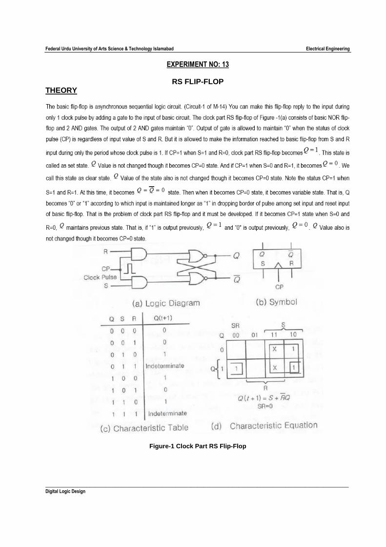
EXPERIMENT NO: 13
RS FLIP-FLOP THEORY
Figure-1 Clock Part RS Flip-Flop
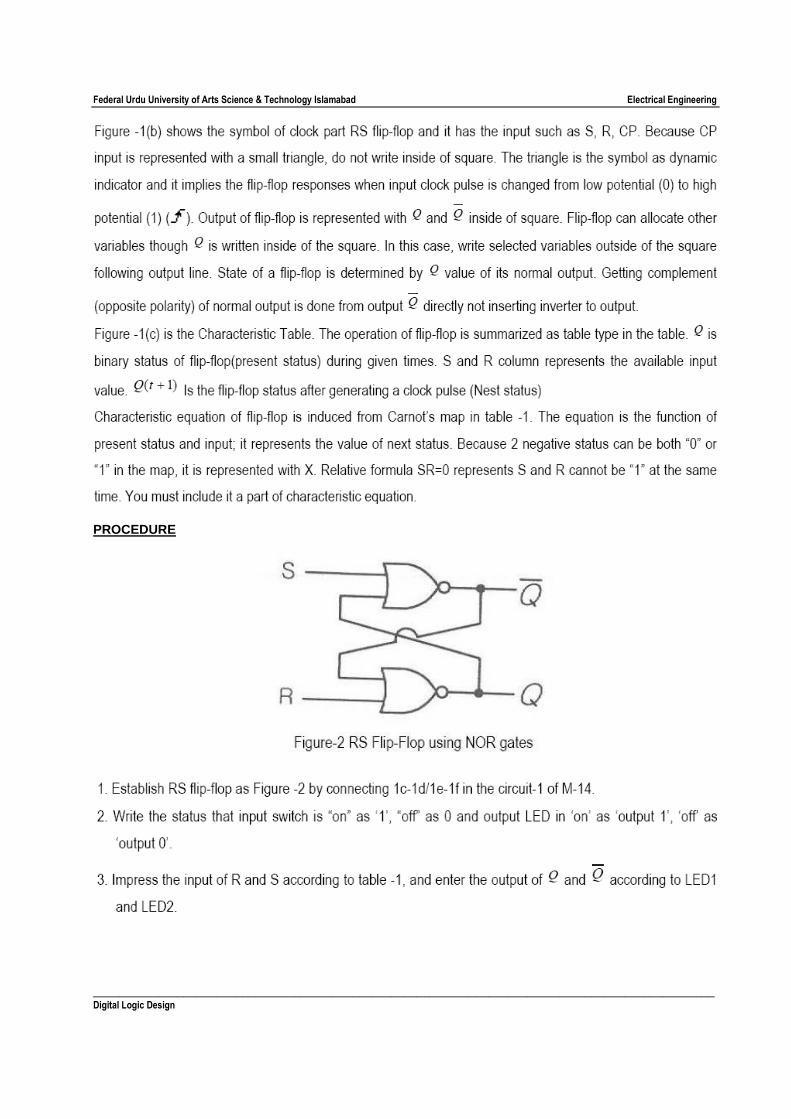
Federal Urdu University of Arts Science & Technology Islamabad Electrical Engineering
________________________________________________________________________________________________ Digital Logic Design
PROCEDURE
Federal Urdu University of Arts Science & Technology Islamabad Electrical Engineering
________________________________________________________________________________________________ Digital Logic Design
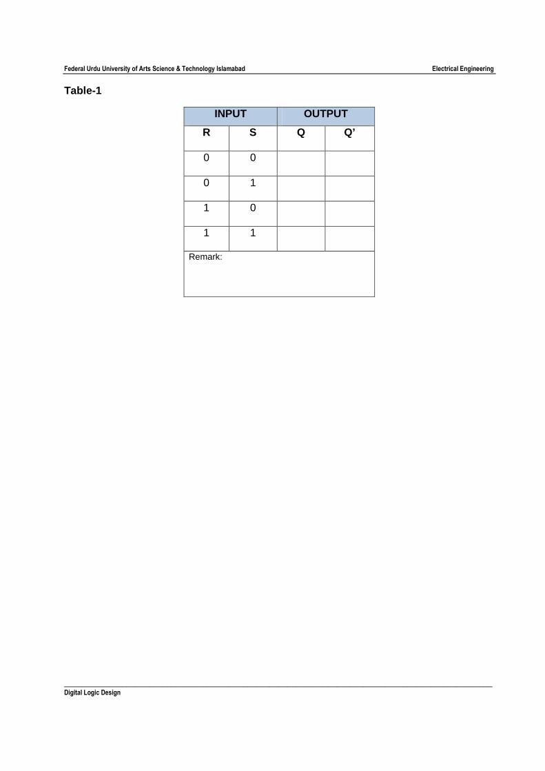
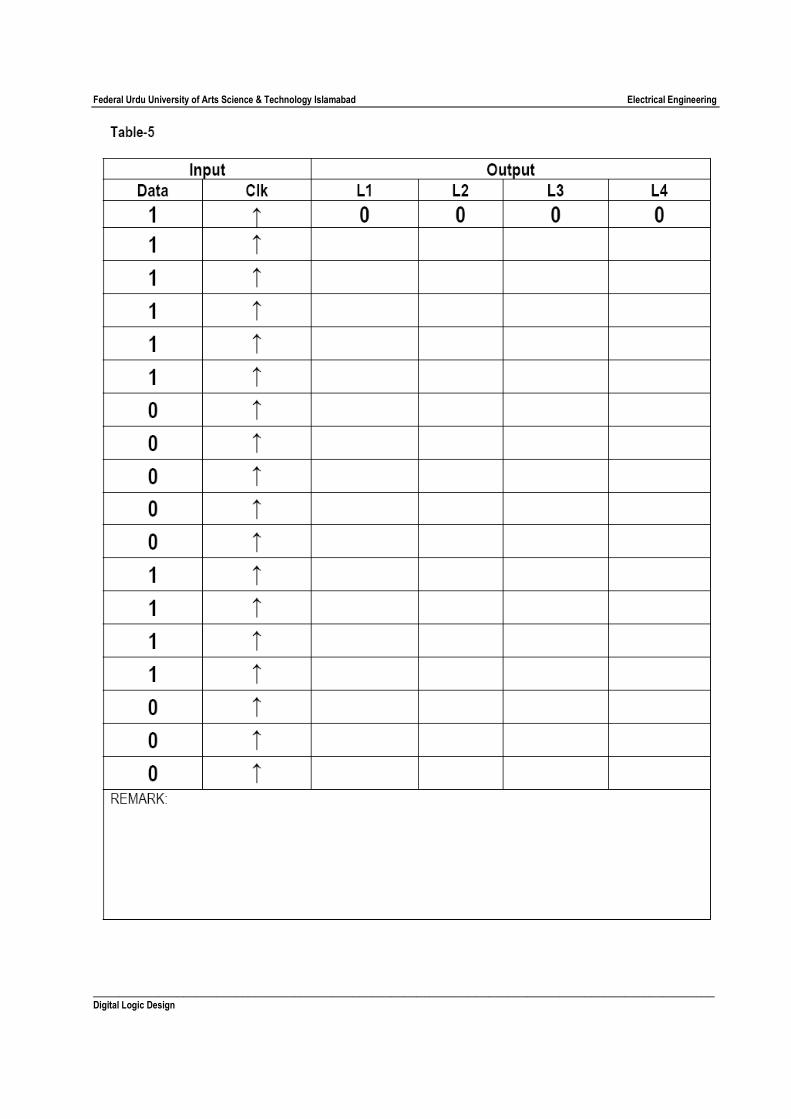
Table-1
INPUT OUTPUT
R S Q Q’
0 0
0 1
1 0
1 1
Remark:
Federal Urdu University of Arts Science & Technology Islamabad Electrical Engineering
________________________________________________________________________________________________ Digital Logic Design
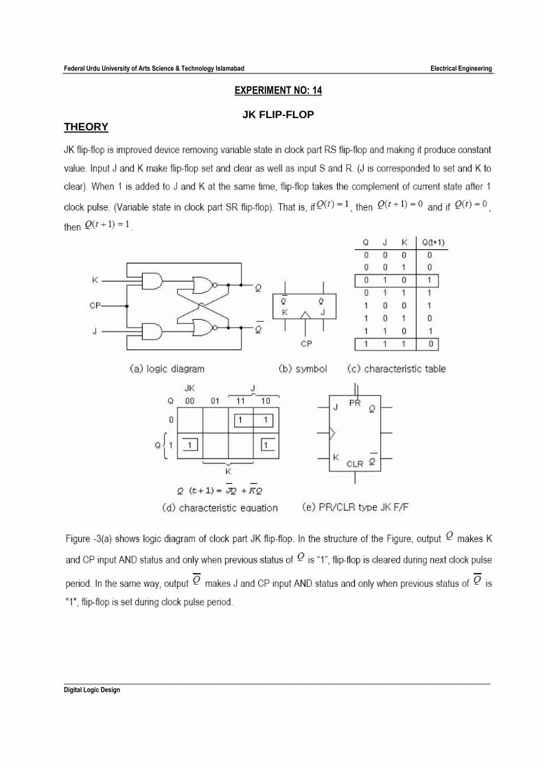
EXPERIMENT NO: 14
JK FLIP-FLOP THEORY
Federal Urdu University of Arts Science & Technology Islamabad Electrical Engineering
________________________________________________________________________________________________ Digital Logic Design
ACT OF JK FLIP-FLOP
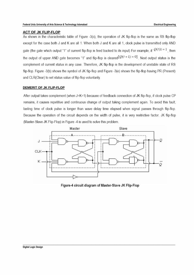
DEMERIT OF JK FLIP-FLOP
Federal Urdu University of Arts Science & Technology Islamabad Electrical Engineering
________________________________________________________________________________________________ Digital Logic Design
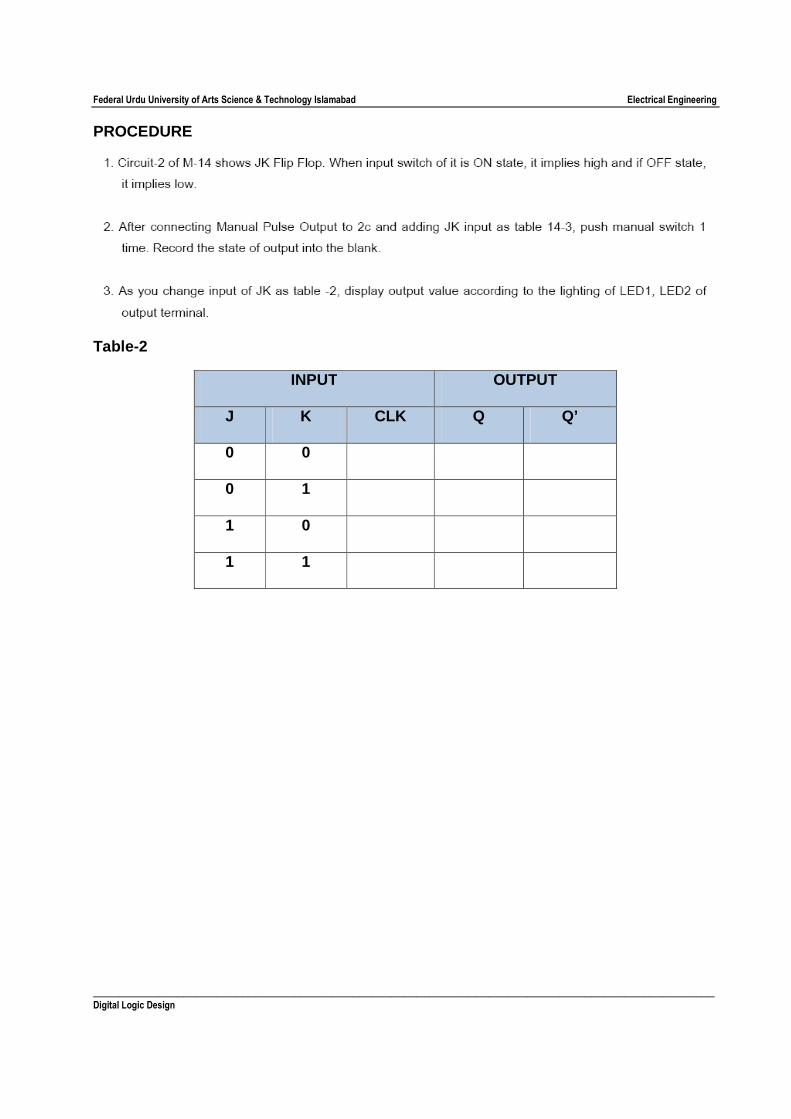
PROCEDURE
Table-2
INPUT OUTPUT
J K CLK Q Q’
0 0
0 1
1 0
1 1
Federal Urdu University of Arts Science & Technology Islamabad Electrical Engineering
________________________________________________________________________________________________ Digital Logic Design
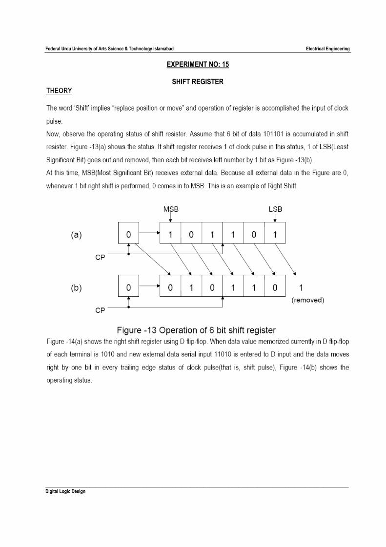
EXPERIMENT NO: 15
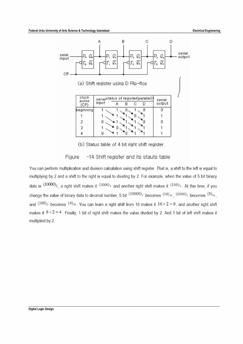
SHIFT REGISTER
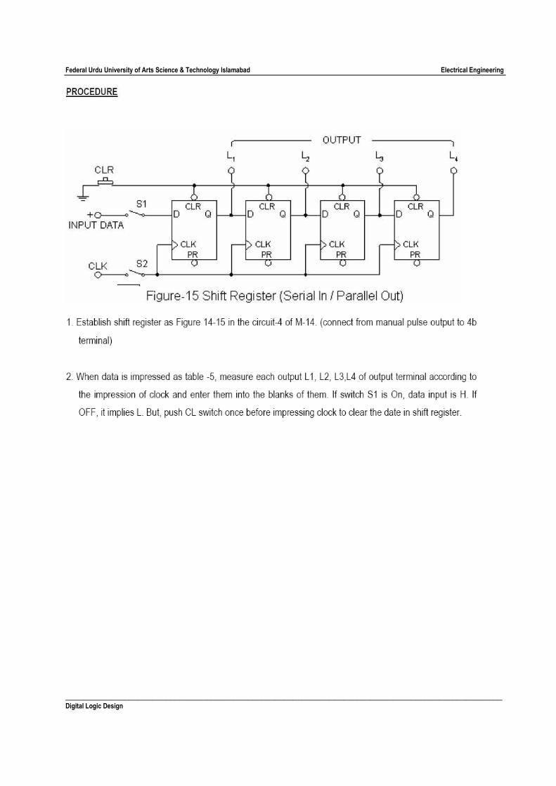
Federal Urdu University of Arts Science & Technology Islamabad Electrical Engineering
________________________________________________________________________________________________ Digital Logic Design
Federal Urdu University of Arts Science & Technology Islamabad Electrical Engineering
________________________________________________________________________________________________ Digital Logic Design
Federal Urdu University of Arts Science & Technology Islamabad Electrical Engineering
________________________________________________________________________________________________ Digital Logic Design

Federal Urdu University of Arts Science & Technology Islamabad Electrical Engineering
________________________________________________________________________________________________ Digital Logic Design
EXPERIMENT NO: 16
BINARY COUNTER THEORY
BINARY RIPPLE COUNTER
Figure- 5 4-bit binary ripple Counter
Figure-6 Calculating order of Binary ripple Counter
Federal Urdu University of Arts Science & Technology Islamabad Electrical Engineering
________________________________________________________________________________________________ Digital Logic Design
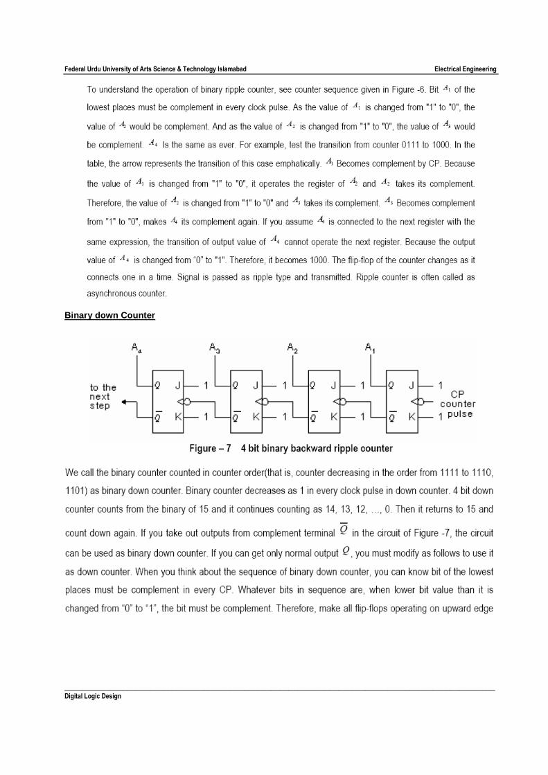
Binary down Counter

Federal Urdu University of Arts Science & Technology Islamabad Electrical Engineering
________________________________________________________________________________________________ Digital Logic Design
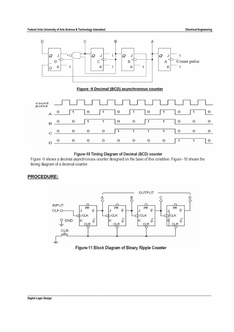
ASYNCHRONOUS DECIMAL(BCD) COUNTER
Federal Urdu University of Arts Science & Technology Islamabad Electrical Engineering
________________________________________________________________________________________________ Digital Logic Design
Figure -9 Decimal (BCD) asynchronous counter
PROCEDURE:

Federal Urdu University of Arts Science & Technology Islamabad Electrical Engineering
________________________________________________________________________________________________ Digital Logic Design

Federal Urdu University of Arts Science & Technology Islamabad Electrical Engineering
________________________________________________________________________________________________ Digital Logic Design
Federal Urdu University of Arts Science & Technology Islamabad Electrical Engineering
________________________________________________________________________________________________ Digital Logic Design
USEFUL ICs THEORY:
IC Family Summary: Various families of logic ICs exist on the market however the families, mainly used in digital electronics lab are
the TTL and the high speed CMOS families.
Nomenclature of digital IC’s:
• MM74XXXNNRP
• MM - Manufacturer
• 74/54 - Temperature range
• XXX - Technology type
• NNN - Logic Function
• R - Revision
• RP - Package Type
Manufacturer - MM
• SN - Texas Instrument, Motorola
• DM - National Semiconductor
Temperature Range – 74 or 54
• 74 - Standard (commercial) 0 to 70ºC
• 54 - Military -55 to 125ºC
Technology Type XXX
• LS – Low power schottky
• ALS – Advanced low power schottky
• Fv -- Fast TTL
• HC -- high speed CMOS
• C -- Low speed CMOS
Vcc It is supply voltage which operate any instrument without damaged. Vcc terminal is always Red.
Ground It is zero potential point, GND terminal is always black.
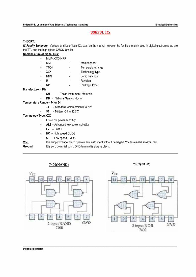
7400(NAND)
7402(NOR)
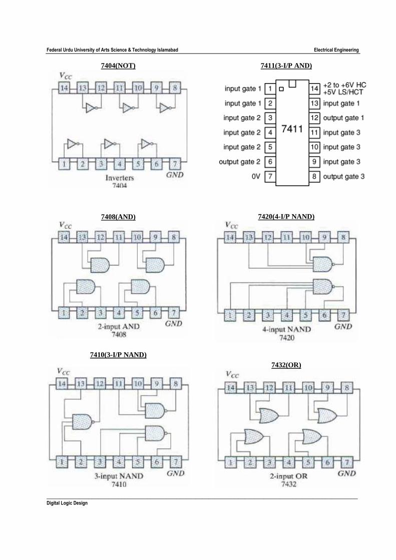
Federal Urdu University of Arts Science & Technology Islamabad Electrical Engineering
________________________________________________________________________________________________ Digital Logic Design
7404(NOT)
7408(AND)
7410(3-I/P NAND)
7411(3-I/P AND)
7420(4-I/P NAND)
7432(OR)
Federal Urdu University of Arts Science & Technology Islamabad Electrical Engineering
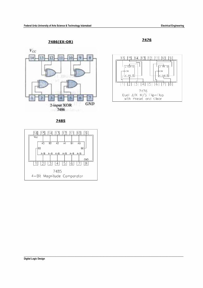
________________________________________________________________________________________________ Digital Logic Design
7486(EX-OR)
7485
7476
Recommended