Power Integrations
5245 Hellyer Avenue, San Jose, CA 95138 USA. Tel: +1 408 414 9200 Fax: +1 408 414 9201
www.powerint.com
Design Example Report
Title 50 W Auxiliary / Standby Supply Using TOP267EG
Specification 90 VAC – 264 VAC (50 Hz) Input; 5 V, 10 A Output
Application Auxiliary / Standby Supply for Laser Printer
Author Applications Engineering Department
Document Number
DER-245
Date February 17, 2010
Revision 1.1 Summary and Features Highly energy efficient
Full load efficiency >82.5% (115 / 230 VAC) Efficiency >78% above 1% load Average efficiency >82% (25%, 50%, 75%, 100% load points) No-load input power <130 mW (<100 mW achievable) Simplifies meeting ENERGY STAR 2.0, 80 Plus and EuP requirements 725 V MOSFET rating allowed high turns ratio (VOR) and use of 40 V Schottky output diode
Low cost, low component count and small PCB footprint solution Performance met without synchronous output rectification 132 kHz operation optimized core size and efficiency performance Low-profile eSIP package
Integrated Protection and Reliability Features Line undervoltage lock out (UVLO) Short circuit protected (via auto-restart) Auto recovery output over current (OCP) Accurate thermal shutdown with large hysteresis
PATENT INFORMATION The products and applications illustrated herein (including transformer construction and circuits external to the products) may be covered by one or more U.S. and foreign patents, or potentially by pending U.S. and foreign patent applications assigned to Power Integrations. A complete list of Power Integrations' patents may be found at www.powerint.com. Power Integrations grants its customers a license under certain patent rights as set forth at <http://www.powerint.com/ip.htm>.

DER-245 50 W Standby/Auxiliary Supply 17-Feb-10
Page 2 of 38
Power Integrations, Inc. Tel: +1 408 414 9200 Fax: +1 408 414 9201 www.powerint.com
Table of Contents 1 Introduction.................................................................................................................4 2 Power Supply Specification ........................................................................................6 3 Schematic...................................................................................................................7 4 Circuit Description ......................................................................................................8
4.1 Input EMI Filtering ...............................................................................................8 4.2 TOPSwitch-JX Primary........................................................................................8 4.3 Output Rectification .............................................................................................8 4.4 Output Feedback.................................................................................................8
5 PCB Layout ................................................................................................................9 6 Bill of Materials .........................................................................................................10 7 Transformer Specification.........................................................................................11
7.1 Electrical Diagram .............................................................................................11 7.2 Electrical Specifications.....................................................................................11 7.3 Materials............................................................................................................11 7.4 Transformer Build Diagram ...............................................................................12 7.5 Transformer Construction..................................................................................13
8 Transformer Design Spreadsheet.............................................................................14 9 Performance Data ....................................................................................................19
9.1 Full Load Efficiency ...........................................................................................19 9.2 Active Mode Efficiency ......................................................................................20 9.3 Light Load Efficiency .........................................................................................21 9.4 DC-DC Efficiency at 380 VDC Input ..................................................................22
9.4.1 Light Load Efficiency (380 VDC Input) .......................................................22 9.4.2 Active Mode Efficiency (380 VDC Input) ....................................................23
9.5 No-load Input Power..........................................................................................24 9.6 Available Standby Output Power.......................................................................25 9.7 Regulation .........................................................................................................26
9.7.1 Load ...........................................................................................................26 9.7.2 Line ............................................................................................................27
10 Thermal Performance ...........................................................................................28 11 Waveforms............................................................................................................29
11.1 Drain Voltage and Current, Normal Operation...................................................29 11.2 Output Voltage Start-up Profile..........................................................................30 11.3 Drain Voltage and Current Start-up Profile ........................................................32 11.4 Load Transient Response .................................................................................33 11.5 Output Ripple Measurements............................................................................34
11.5.1 Ripple Measurement Technique ................................................................34 11.5.2 Measurement Results ................................................................................35
12 Control Loop Measurements.................................................................................36 12.1 115 VAC............................................................................................................36 12.2 230 VAC............................................................................................................36
13 Revision History ....................................................................................................37

17-Feb-10 DER-245 50 W Standby/Auxiliary Supply
Page 3 of 38
Power Integrations Tel: +1 408 414 9200 Fax: +1 408 414 9201
www.powerint.com
Important Note: Although this board is designed to satisfy safety isolation requirements, the engineering prototype has not been agency approved. Therefore, all testing should be performed using an isolation transformer to provide the AC input to the prototype board.

DER-245 50 W Standby/Auxiliary Supply 17-Feb-10
Page 4 of 38
Power Integrations, Inc. Tel: +1 408 414 9200 Fax: +1 408 414 9201 www.powerint.com
1 Introduction This document is an engineering report describing a 50 W power supply utilizing a TOP267EG. This power supply achieves >80% efficiency at 100 VAC 50Hz, full load output current of 10 A without employing secondary synchronous rectification. The EMI section is not designed for a typical 50 W power supply. The EMI components were chosen to resemble the input stage of a 200 W power supply unit. This is done to simulate EMI stage losses for a typical 200 W PSU in which this flyback converter will be the standby / auxiliary section of a complete system PSU. A 10ohm NTC is also employed to include the additional losses associated with any inrush limiting in the final system.

17-Feb-10 DER-245 50 W Standby/Auxiliary Supply
Page 5 of 38
Power Integrations Tel: +1 408 414 9200 Fax: +1 408 414 9201
www.powerint.com
Figure 1 – Populated Circuit Board Photograph.

DER-245 50 W Standby/Auxiliary Supply 17-Feb-10
Page 6 of 38
Power Integrations, Inc. Tel: +1 408 414 9200 Fax: +1 408 414 9201 www.powerint.com
2 Power Supply Specification The table below represents the minimum acceptable performance of the design. Actual performance is listed in the results section.
Description Symbol Min Typ Max Units Comment
Input
AC Voltage VIN 90 264 VAC 2 Wire – no P.E.
Frequency fLINE 50 Hz
DC VIN(DC) 380 390 VDC
No-load Input Power (230 VAC) 0.3 W
Output
Output Voltage 1 VOUT1 5 V 5%
Output Ripple Voltage 1 VRIPPLE1 200 mV 20 MHz bandwidth
Output Current 1 IOUT1 0 10 A
Total Output Power
Continuous Output Power POUT 50 W
Efficiency
Full Load 80 % Measured at POUT 25 oC

17-Feb-10 DER-245 50 W Standby/Auxiliary Supply
Page 7 of 38
Power Integrations Tel: +1 408 414 9200 Fax: +1 408 414 9201
www.powerint.com
3 Schematic
Figure 2 – Schematic Diagram.

DER-245 50 W Standby/Auxiliary Supply 17-Feb-10
Page 8 of 38
Power Integrations, Inc. Tel: +1 408 414 9200 Fax: +1 408 414 9201 www.powerint.com
4 Circuit Description The circuit is built around a TOP267EG device from the TOPSwitch-JX family; a highly integrated monolithic off-line switcher IC designed for providing high-efficiency under all load conditions and very low no-load input power.
4.1 Input EMI Filtering The EMI section of this unit consists of C1 (and associated discharge resistors R1 and R2) and L3. The filter stage was not designed and tested to meet conducted and radiated emissions standards. Instead it was included to represent the losses in the EMI filter for a 200 W output supply in which this 50 W design is the auxiliary / standby converter.
4.2 TOPSwitch-JX Primary The TOP267EG is configured to operate at its full frequency mode (132 kHz) during heavy loading condition by shorting the F pin to the S pin. The 132 kHz operation reduces the maximum primary rms current by allowing more deeply continuous operation (lower value of KP) and thus helps to improve efficiency by lowering conduction losses. Compared to operation at 66 kHz, this can be achieved without excessive transformer turns or a larger core size. At high input voltages (400 VDC), the converter operates in critically discontinuous conduction mode which reduces switching losses of the TOPSwitch-JX and the reverse recovery losses associated with the secondary rectifier. A 4 M ohm total resistance connected to the V pin enables the UV/OV feature of the IC. Resistor R7 is also connected between X pin and S pin to lower the current limit to 60% and prevents the transformer from saturating during start-up and short circuit conditions. The 10.5 k ohm resistor sets the peak flux density to < 3600 Gauss.
4.3 Output Rectification The T1 output is rectified and filtered by D4, C9, and C10. Diode D4 is a low drop power Schottky rectifier with 40 V PIV rating. The transformer is designed to have lower secondary PIV to minimize secondary diode conduction losses. Capacitors C9 and C10 are high ripple current, ultra low ESR capacitors in a small package. Capacitors C9 and C10 were chosen to minimize board space requirement for the output capacitors and at the same time cater for the secondary ripple current. Post filter L2 and C12 provide high frequency output filtering.
4.4 Output Feedback
Resistors R13 and R15 are used to set the output voltage. Shunt regulator U2 drives optocoupler U3 through resistor R12 to provide feedback information to the U1 control pin. Components C13, C14, and R3 provide frequency compensation for the error amplifier U2.

17-Feb-10 DER-245 50 W Standby/Auxiliary Supply
Page 9 of 38
Power Integrations Tel: +1 408 414 9200 Fax: +1 408 414 9201
www.powerint.com
5 PCB Layout
Figure 3 – Printed Circuit Layout (2.5 in x 4.2 in).

DER-245 50 W Standby/Auxiliary Supply 17-Feb-10
Page 10 of 38
Power Integrations, Inc. Tel: +1 408 414 9200 Fax: +1 408 414 9201 www.powerint.com
6 Bill of Materials
Item Qty Ref Des Description Mfg Part Number Mfg
1 1 BR1 800 V, 8 A, Bridge Rectifier, GBU Case GBU8K Vishay
2 1 C1 330 nF, 275 VAC, Film, X2 LE334-M OKAYA
3 1 C2 120 F, 400 V, Electrolytic, (18 x 30) EPAG401ELL121MM30S Nippon Chemi-Con
4 1 C4 2.2 nF, 1 kV, Disc Ceramic NCD222K1KVY5FF NIC Components
5 2 C5 C13 100 nF, 50 V, Ceramic, X7R RPER71H104K2K1A03B Murata
6 1 C6 47 F, 50 V, Electrolytic, Gen. Purpose, (6.3 x 11) EKMG500ELL470MF11D Nippon Chemi-Con
7 1 C7 22 F, 50 V, Electrolytic, Very Low ESR, 340 m, (5 x 11)
EKZE500ELL220ME11D Nippon Chemi-Con
8 1 C8 470 pF, 100 V, Ceramic, X7R B37981M1471M000 Epcos
9 2 C9 C10 680 F, 10 V, Super Low ESR, 7 m, (16 x 20) APSC100ELL681MJB5S Nippon Chemi-Con
10 1 C12 220 F, 25 V, Electrolytic, Very Low ESR, 72 m, (8 x 11.5)
EKZE250ELL221MHB5D Nippon Chemi-Con
11 1 C14 10 nF, 100 V, Ceramic, X7R B37981M1103K000 Epcos
12 1 C15 4.7 F, 50 V, Electrolytic, Gen. Purpose, (5 x 11) EKMG500ELL4R7ME11D Nippon Chemi-Con
13 1 CY1 2.2 nF, Ceramic, Y1 440LD22-R Vishay
14 1 D1 800 V, 1 A, Fast Recovery Diode, 500 ns, DO-41 FR106 Diodes Inc.
15 1 D2 250 V, 250 mA, Fast Switching, DO-35 BAV21 Vishay
16 1 D4 40 V, 40 A, Dual Schotkky, TO-220AB STPS40L40CT ST
17 1 F1 2 A, 250 V, Slow, TR5 3721200041 Wickman
18 2 J1 J2 2 Position (1 x 2) header, 0.312 pitch, Vertical 26-50-3039 Molex
19 1 JP1 Wire Jumper, Non insulated, 22 AWG, 0.2 in 298 Alpha
20 1 L2 1 H
21 1 L3 Common Mode Choke Toroidal P/N T22148-902S Fontaine Tech
22 2 R1 R2 1.5 M, 5%, 1/4 W, Carbon Film CFR-25JB-1M5 Yageo
23 1 R3 165 , 1%, 1/4 W, Metal Film MFR-25FBF-165R Yageo
24 2 R5 R6 2.0 M, 5%, 1/4 W, Carbon Film CFR-25JB-2M0 Yageo
25 1 R7 10.5 k, 1%, 1/4 W, Metal Film MFR-25FBF-10K5 Yageo
26 1 R8 75 , 5%, 1/2 W, Carbon Film CFR-50JB-75R Yageo
27 1 R10 6.8 , 5%, 1/8 W, Carbon Film CFR-12JB-6R8 Yageo
28 1 R11 22 , 5%, 1/4 W, Carbon Film CFR-25JB-22R Yageo
29 1 R12 1.5 k, 1%, 1/4 W, Metal Film MFR-25FBF-1K50 Yageo
30 3 R13 R15
R20 10 k, 1%, 1/4 W, Metal Film ERO-S2PHF1002 Panasonic
31 1 RT1 NTC Thermistor, 10 Ohms, 3.2 A CL-110 Thermometrics
32 1 T1 Bobbin, PQ26/25, Vertical, 12 pins BPQ26/25-1112CPFR TDK
33 1 U1 TOPSwitch-JX, TOP267EG, eSIP-7C TOP267EG Power Integrations
34 1 U2 2.495 V Shunt Regulator IC, 2%, 0 to 70C, TO-92 TL431CLPG On Semiconductor
35 1 U3 Optocoupler, 35 V, CTR 300-600%, 4-DIP LTV-817D Liteon
36 1 VR2 180 V, 5 W, 5%, TVS, DO204AC (DO-15) P6KE180ARLG On Semi

17-Feb-10 DER-245 50 W Standby/Auxiliary Supply
Page 11 of 38
Power Integrations Tel: +1 408 414 9200 Fax: +1 408 414 9201
www.powerint.com
7 Transformer Specification
7.1 Electrical Diagram
Figure 4 – Transformer Electrical Diagram.
7.2 Electrical Specifications
Electrical Strength 1 second, 60 Hz, from pins 1, 2, 3, 4, 6 to pins 7, 8, 9, 10, 11, 12
3000 VAC
Primary Inductance Pins 1-3, all other windings open 653 H, 10% Primary Leakage Inductance Pins 1-3, with all other windings shorted 10 H (Max.)
7.3 Materials Item Description [1] Core: PQ2625, NC-2H (Nicera) or equivalent, gapped for ALG of 406 nH/t² [2] Bobbin: BPQ26/25-1112CPFR [3] Barrier tape: Polyester film (1 mil base thickness), 13.80 mm wide [4] Varnish [5] Triple Insulated Wire: #26 AWG
[6] Copper Foil: 10 mil thick, 12.5 mm wide, covered with 1 layer of lapped tape. Terminations to foil: 4 x #19 AWG magnet wire with sleeving
[7] #19 AWG magnet wire

DER-245 50 W Standby/Auxiliary Supply 17-Feb-10
Page 12 of 38
Power Integrations, Inc. Tel: +1 408 414 9200 Fax: +1 408 414 9201 www.powerint.com
7.4 Transformer Build Diagram
Figure 5 – Transformer Build Diagram.
Figure 6 – Copper Foil Winding.

17-Feb-10 DER-245 50 W Standby/Auxiliary Supply
Page 13 of 38
Power Integrations Tel: +1 408 414 9200 Fax: +1 408 414 9201
www.powerint.com
7.5 Transformer Construction Primary Winding
(Section 1)
Start on pin(s) 3 and wind 20 turns (x 1 filar) of item [5] in 1 layer(s) from left to right. Finish this winding on pin(s) 2. Add 1 layer of tape, item [3].
Bias Winding Start on pin(s) 6 and wind 6 turns (x 1 filar) of item [5]. Wind in same rotational direction as primary winding. Spread the winding evenly across entire bobbin. Finish this winding on pin(s) 4. Add 1 layer of tape, item [3].
Secondary Winding
Start on pin(s) 10, 11, 12 and wind 2 turns of item [6]. Wind in same rotational direction as primary winding. Finish this winding on pin(s) 7, 8, 9. Add 1 layers of tape, item [3].
Primary Winding
(Section 2)
Start on pin(s) 2 and wind 20 turns (x 1 filar) of item [5] in 1 layer(s) from left to right. Finish this winding on pin(s) 1.Add 1 layers of tape, item [3].
Core Assembly Assemble and secure core halves. Item [1]. Varnish Dip varnish uniformly in item [4]. Do not vacuum impregnate.

DER-245 50 W Standby/Auxiliary Supply 17-Feb-10
Page 14 of 38
Power Integrations, Inc. Tel: +1 408 414 9200 Fax: +1 408 414 9201 www.powerint.com
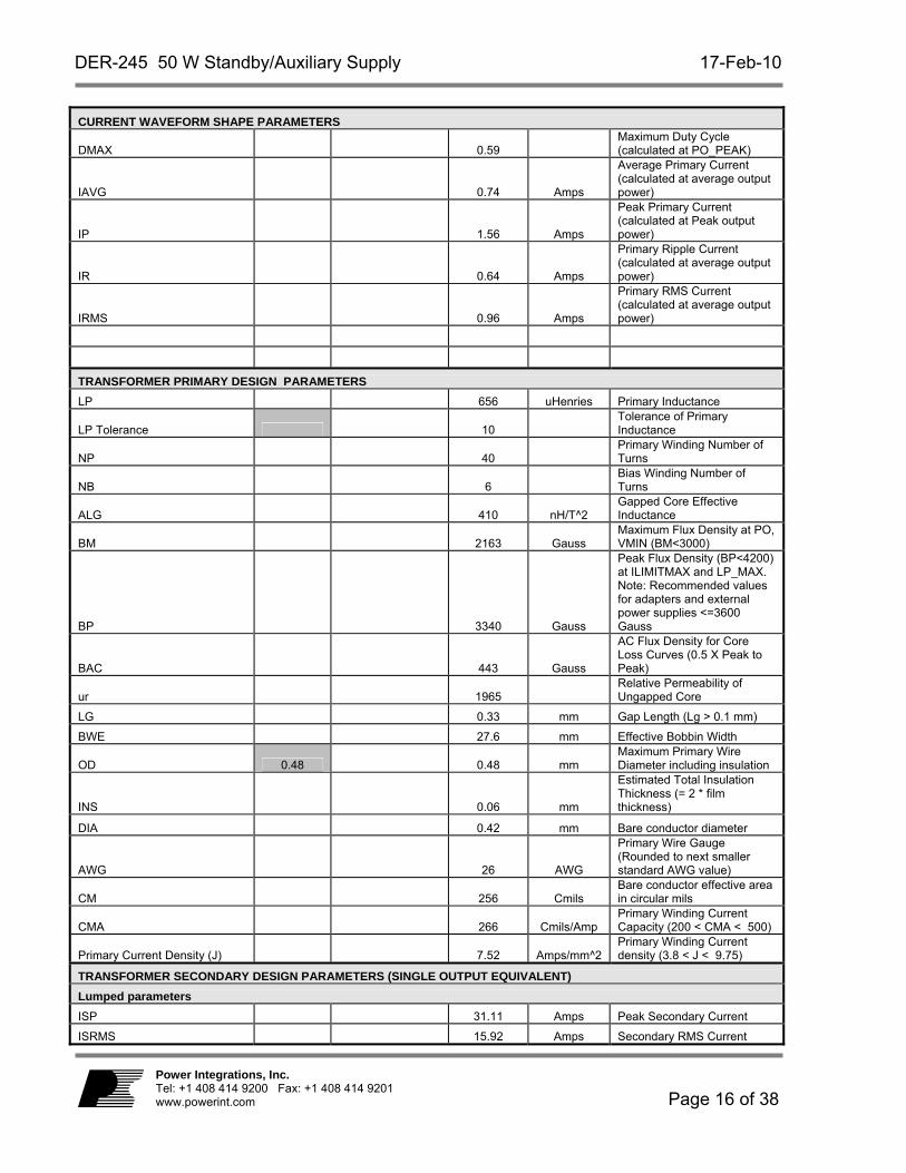
8 Transformer Design Spreadsheet
ACDC_TOPSwitchJX_120709; Rev.1.1; Copyright Power
Integrations 2009 INPUT INFO OUTPUT UNIT
TOP_JX_120709: TOPSwitch-JX
Continuous/Discontinuous Flyback Transformer Design Spreadsheet
ENTER APPLICATION VARIABLES
VACMIN 90 Volts Minimum AC Input Voltage
VACMAX 264 Volts Maximum AC Input Voltage
fL 50 Hertz AC Mains Frequency
VO 5.00 Volts Output Voltage (main)
PO_AVG 50.00 Watts Average Output Power
PO_PEAK 50.00 50.00 Watts Peak Output Power
Heatsink Type External External Heatsink Type
Enclosure Open Frame
Open Frame enclosure assume sufficient airflow while adapter means a sealed enclosure.
n 0.80 %/100 Efficiency Estimate
Z 0.48 Loss Allocation Factor
VB 15 Volts Bias Voltage - Verify that VB is > 8 V at no load and VMAX
tC 3.00 ms Bridge Rectifier Conduction Time Estimate
CIN 120.0 120 uFarads Input Filter Capacitor
ENTER TOPSWITCH-JX VARIABLES
TOPSwitch-JX TOP267E Universal /
Peak 115 Doubled/230V
Chosen Device TOP267E Power Out 103 W / 103
W 137W
KI 0.68
External Ilimit reduction factor (KI=1.0 for default ILIMIT, KI <1.0 for lower ILIMIT)
ILIMITMIN_EXT 1.898 Amps Use 1% resistor in setting external ILIMIT
ILIMITMAX_EXT 2.184 Amps Use 1% resistor in setting external ILIMIT
Frequency (F)=132kHz, (H)=66kHz F F
Select 'H' for Half frequency - 66kHz, or 'F' for Full frequency - 132kHz
fS 132000 Hertz
TOPSwitch-JX Switching Frequency: Choose between 132 kHz and 66 kHz
fSmin 119000 Hertz TOPSwitch-JX Minimum Switching Frequency
fSmax 145000 Hertz TOPSwitch-JX Maximum Switching Frequency
High Line Operating Mode FF Full Frequency, Jitter enabled
VOR 110.00 Volts Reflected Output Voltage
VDS 10 Volts TOPSwitch on-state Drain to Source Voltage
VD 0.50 Volts Output Winding Diode Forward Voltage Drop
VDB 0.70 Volts Bias Winding Diode Forward Voltage Drop
KP 0.41 Ripple to Peak Current Ratio (0.3 < KRP < 1.0 : 1.0<

17-Feb-10 DER-245 50 W Standby/Auxiliary Supply
Page 15 of 38
Power Integrations Tel: +1 408 414 9200 Fax: +1 408 414 9201
www.powerint.com
KDP<6.0)
PROTECTION FEATURES
LINE SENSING V pin functionality
VUV_STARTUP 95.00 72 Volts
Minimum DC Bus Voltage at which the power supply will start-up
VOV_SHUTDOWN 356 Volts
Typical DC Bus Voltage at which power supply will shut-down (Max)
RLS 3.2 M-ohms
Use two standard, 1.6 M-Ohm, 5% resistors in series for line sense functionality.
OUTPUT OVERVOLTAGE
VZ 27 Volts
Zener Diode rated voltage for Output Overvoltage shutdown protection
RZ 5.1 k-ohms
Output OVP resistor. For latching shutdown use 20 ohm resistor instead
OVERLOAD POWER LIMITING X pin functionality
Overload Current Ratio at VMAX 1.20 1.2
Enter the desired margin to current limit at VMAX. A value of 1.2 indicates that the current limit should be 20% higher than peak primary current at VMAX
Overload Current Ratio at VMIN Info 1.22
Your margin to current limit at low line is high. Reduce KI to 0.55 (if possible).
ILIMIT_EXT_VMIN 1.56 A Peak primary Current at VMIN
ILIMIT_EXT_VMAX 1.03 A Peak Primary Current at VMAX
RIL 9.36 k-ohms Current limit/Power Limiting resistor.
RPL N/A M-ohms Resistor not required. Use RIL resistor only
ENTER TRANSFORMER CORE/CONSTRUCTION VARIABLES
Core Type PQ2625 PQ2625 Core Type
Core PQ2625 P/N: PC44PQ26/25Z-12
Bobbin PQ2625_BOBBIN P/N: *
AE 1.18 cm^2 Core Effective Cross Sectional Area
LE 5.55 cm Core Effective Path Length
AL 5250 nH/T^2 Ungapped Core Effective Inductance
BW 13.8 mm Bobbin Physical Winding Width
M 0.00 mm
Safety Margin Width (Half the Primary to Secondary Creepage Distance)
L 2.00 Number of Primary Layers
NS 2 2 Number of Secondary Turns
DC INPUT VOLTAGE PARAMETERS
VMIN 85 85 Volts Minimum DC Input Voltage
VMAX 400 400 Volts Maximum DC Input Voltage
DER-245 50 W Standby/Auxiliary Supply 17-Feb-10
Page 16 of 38
Power Integrations, Inc. Tel: +1 408 414 9200 Fax: +1 408 414 9201 www.powerint.com
CURRENT WAVEFORM SHAPE PARAMETERS
DMAX 0.59 Maximum Duty Cycle (calculated at PO_PEAK)
IAVG 0.74 Amps
Average Primary Current (calculated at average output power)
IP 1.56 Amps
Peak Primary Current (calculated at Peak output power)
IR 0.64 Amps
Primary Ripple Current (calculated at average output power)
IRMS 0.96 Amps
Primary RMS Current (calculated at average output power)
TRANSFORMER PRIMARY DESIGN PARAMETERS
LP 656 uHenries Primary Inductance
LP Tolerance 10 Tolerance of Primary Inductance
NP 40 Primary Winding Number of Turns
NB 6 Bias Winding Number of Turns
ALG 410 nH/T^2 Gapped Core Effective Inductance
BM 2163 Gauss Maximum Flux Density at PO, VMIN (BM<3000)
BP 3340 Gauss
Peak Flux Density (BP<4200) at ILIMITMAX and LP_MAX. Note: Recommended values for adapters and external power supplies <=3600 Gauss
BAC 443 Gauss
AC Flux Density for Core Loss Curves (0.5 X Peak to Peak)
ur 1965 Relative Permeability of Ungapped Core
LG 0.33 mm Gap Length (Lg > 0.1 mm)
BWE 27.6 mm Effective Bobbin Width
OD 0.48 0.48 mm Maximum Primary Wire Diameter including insulation
INS 0.06 mm
Estimated Total Insulation Thickness (= 2 * film thickness)
DIA 0.42 mm Bare conductor diameter
AWG 26 AWG
Primary Wire Gauge (Rounded to next smaller standard AWG value)
CM 256 Cmils Bare conductor effective area in circular mils
CMA 266 Cmils/Amp Primary Winding Current Capacity (200 < CMA < 500)
Primary Current Density (J) 7.52 Amps/mm^2 Primary Winding Current density (3.8 < J < 9.75)
TRANSFORMER SECONDARY DESIGN PARAMETERS (SINGLE OUTPUT EQUIVALENT)
Lumped parameters
ISP 31.11 Amps Peak Secondary Current
ISRMS 15.92 Amps Secondary RMS Current

17-Feb-10 DER-245 50 W Standby/Auxiliary Supply
Page 17 of 38
Power Integrations Tel: +1 408 414 9200 Fax: +1 408 414 9201
www.powerint.com
IO_PEAK 10.00 Amps Secondary Peak Output Current
IO 10.00 Amps Average Power Supply Output Current
IRIPPLE 12.39 Amps Output Capacitor RMS Ripple Current
CMS 3184 Cmils Secondary Bare Conductor minimum circular mils
AWGS 15 AWG
Secondary Wire Gauge (Rounded up to next larger standard AWG value)
DIAS 1.45 mm Secondary Minimum Bare Conductor Diameter
ODS 6.90 mm
Secondary Maximum Outside Diameter for Triple Insulated Wire
INSS 2.72 mm Maximum Secondary Insulation Wall Thickness
VOLTAGE STRESS PARAMETERS
VDRAIN 618 Volts
Maximum Drain Voltage Estimate (Includes Effect of Leakage Inductance)
PIVS 25 Volts Output Rectifier Maximum Peak Inverse Voltage
PIVB 72 Volts Bias Rectifier Maximum Peak Inverse Voltage
TRANSFORMER SECONDARY DESIGN PARAMETERS (MULTIPLE OUTPUTS)
1st output
VO1 5 Volts Output Voltage
IO1_AVG 10.00 Amps Average DC Output Current
PO1_AVG 50.00 Watts Average Output Power
VD1 0.5 Volts Output Diode Forward Voltage Drop
NS1 2.00 Output Winding Number of Turns
ISRMS1 15.921 Amps Output Winding RMS Current
IRIPPLE1 12.39 Amps Output Capacitor RMS Ripple Current
PIVS1 25 Volts Output Rectifier Maximum Peak Inverse Voltage
CMS1 3184 Cmils
Output Winding Bare Conductor minimum circular mils
AWGS1 15 AWG
Wire Gauge (Rounded up to next larger standard AWG value)
DIAS1 1.45 mm Minimum Bare Conductor Diameter
ODS1 6.90 mm Maximum Outside Diameter for Triple Insulated Wire
2nd output
VO2 Volts Output Voltage
IO2_AVG Amps Average DC Output Current
PO2_AVG 0.00 Watts Average Output Power
VD2 0.7 Volts Output Diode Forward Voltage Drop
NS2 0.25 Output Winding Number of Turns
ISRMS2 0.000 Amps Output Winding RMS Current
IRIPPLE2 0.00 Amps Output Capacitor RMS Ripple Current

DER-245 50 W Standby/Auxiliary Supply 17-Feb-10
Page 18 of 38
Power Integrations, Inc. Tel: +1 408 414 9200 Fax: +1 408 414 9201 www.powerint.com
PIVS2 3 Volts Output Rectifier Maximum Peak Inverse Voltage
CMS2 0 Cmils
Output Winding Bare Conductor minimum circular mils
AWGS2 N/A AWG
Wire Gauge (Rounded up to next larger standard AWG value)
DIAS2 N/A mm Minimum Bare Conductor Diameter
ODS2 N/A mm Maximum Outside Diameter for Triple Insulated Wire
3rd output
VO3 Volts Output Voltage
IO3_AVG Amps Average DC Output Current
PO3_AVG 0.00 Watts Average Output Power
VD3 0.70 Volts Output Diode Forward Voltage Drop
NS3 0.25 Output Winding Number of Turns
ISRMS3 0.000 Amps Output Winding RMS Current
IRIPPLE3 0.00 Amps Output Capacitor RMS Ripple Current
PIVS3 3 Volts Output Rectifier Maximum Peak Inverse Voltage
CMS3 0 Cmils
Output Winding Bare Conductor minimum circular mils
AWGS3 N/A AWG
Wire Gauge (Rounded up to next larger standard AWG value)
DIAS3 N/A mm Minimum Bare Conductor Diameter
ODS3 N/A mm Maximum Outside Diameter for Triple Insulated Wire
Total Continuous Output Power 50 Watts
Total Continuous Output Power
Negative Output N/A
If negative output exists enter Output number; eg: If VO2 is negative output, enter 2

17-Feb-10 DER-245 50 W Standby/Auxiliary Supply
Page 19 of 38
Power Integrations Tel: +1 408 414 9200 Fax: +1 408 414 9201
www.powerint.com
9 Performance Data All measurements performed at room temperature and 50 Hz input frequency for AC input.
9.1 Full Load Efficiency
79.85
81.23
82.55
83.49
84.15
84.76 84.9685.09
85.14
85.12
78
80
82
84
86
88
85 105 125 145 165 185 205 225 245 265
Input Voltage (VAC)
Eff
icie
ncy
(%
)
Figure 7 – Efficiency vs. Input Voltage, Room Temperature, 50 Hz.
Full Load Efficiency
VIN (VAC, 50 Hz)
PIN (W)
VOUT (V)
IOUT (A)
Efficiency (%)
90 62.62 5.00 10 79.85
100 61.55 5.00 10 81.23
115 60.57 5.00 10 82.55
132 59.89 5.00 10 83.49
150 59.42 5.00 10 84.15
180 58.99 5.00 10 84.76
200 58.85 5.00 10 84.96
230 58.74 5.00 10 85.12
240 58.73 5.00 10 85.14
264 58.76 5.00 10 85.09
DER-245 50 W Standby/Auxiliary Supply 17-Feb-10
Page 20 of 38
Power Integrations, Inc. Tel: +1 408 414 9200 Fax: +1 408 414 9201 www.powerint.com
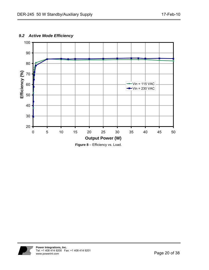
9.2 Active Mode Efficiency
20
30
40
50
60
70
80
90
100
0 5 10 15 20 25 30 35 40 45 50
Output Power (W)
Eff
icie
ncy
(%
)
Vin = 115 VACVin = 230 VAC
Figure 8 – Efficiency vs. Load.

17-Feb-10 DER-245 50 W Standby/Auxiliary Supply
Page 21 of 38
Power Integrations Tel: +1 408 414 9200 Fax: +1 408 414 9201
www.powerint.com
9.3 Light Load Efficiency
20
30
40
50
60
70
80
90
100
0 0.5 1 1.5 2 2.5 3 3.5 4 4.5 5
Output Power (W)
Eff
icie
ncy
(%
)
Vin = 100 VACVin = 115 VAC
Vin = 230 VAC
Figure 9 – Efficiency vs. Load.
AC-DC Light Load Efficiency Table
POUT (W) 100 VAC 115 VAC 230 VAC
0.05 38.00% 37.61% 29.36%
0.1 52.77% 52.31% 43.84%
0.2 65.46% 64.97% 57.90%
0.3 71.15% 71.16% 64.80%
0.4 74.48% 74.32% 69.07%
0.5 76.57% 76.35% 71.85%
1 81.04% 80.95% 78.12%
5 84.13% 84.51% 84.16%

DER-245 50 W Standby/Auxiliary Supply 17-Feb-10
Page 22 of 38
Power Integrations, Inc. Tel: +1 408 414 9200 Fax: +1 408 414 9201 www.powerint.com
9.4 DC-DC Efficiency at 380 VDC Input The DC-DC stage efficiency measurements were taken at light load to full load conditions at room temperature. 380 VDC was applied across the Bulk Capacitor C2 with RT1 removed.
9.4.1 Light Load Efficiency (380 VDC Input)
43.40
28.78
57.44
84.79
71.55
68.63
64.57
78.17
20
30
40
50
60
70
80
90
100
0 0.5 1 1.5 2 2.5 3 3.5 4 4.5 5
Output Power (W)
Eff
icie
ncy
(%
)
Figure 10 – DC-DC Efficiency vs. Load.
DC-DC Light Load Efficiency Table
POUT (W) 0 0.1 0.2 0.3 0.4 0.5 1 5
Efficiency (%) 28.78 43.40 57.44 64.57 68.63 71.55 78.17 84.79

17-Feb-10 DER-245 50 W Standby/Auxiliary Supply
Page 23 of 38
Power Integrations Tel: +1 408 414 9200 Fax: +1 408 414 9201
www.powerint.com
9.4.2 Active Mode Efficiency (380 VDC Input)
43.40
57.44
64.57
71.5568.63
28.78
78.17
84.79
85.53 85.57 85.59 85.86 86.00 86.19
86.24
86.41 86.57 86.76
86.22
20
30
40
50
60
70
80
90
100
0 5 10 15 20 25 30 35 40 45 50
Output Power (W)
Eff
icie
ncy
(%
)
Figure 11 – DC-DC Efficiency vs. Load.
DER-245 50 W Standby/Auxiliary Supply 17-Feb-10
Page 24 of 38
Power Integrations, Inc. Tel: +1 408 414 9200 Fax: +1 408 414 9201 www.powerint.com
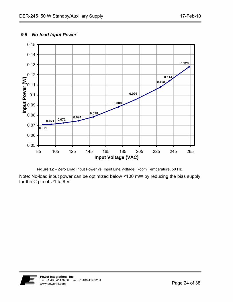
9.5 No-load Input Power
0.088
0.071
0.071 0.0720.074
0.078
0.096
0.108
0.114
0.128
0.05
0.06
0.07
0.08
0.09
0.1
0.11
0.12
0.13
0.14
0.15
85 105 125 145 165 185 205 225 245 265
Input Voltage (VAC)
Inp
ut
Po
wer
(W
)
Figure 12 – Zero Load Input Power vs. Input Line Voltage, Room Temperature, 50 Hz.
Note: No-load input power can be optimized below <100 mW by reducing the bias supply for the C pin of U1 to 8 V.
17-Feb-10 DER-245 50 W Standby/Auxiliary Supply
Page 25 of 38
Power Integrations Tel: +1 408 414 9200 Fax: +1 408 414 9201
www.powerint.com
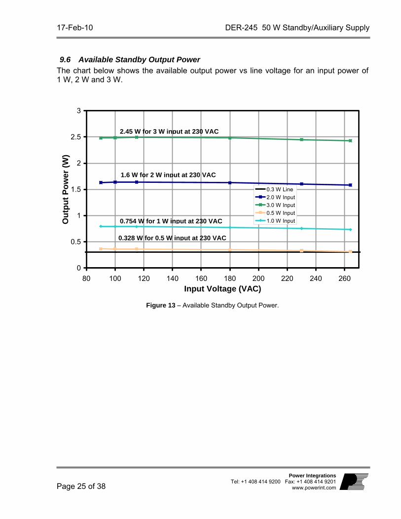
9.6 Available Standby Output Power The chart below shows the available output power vs line voltage for an input power of 1 W, 2 W and 3 W.
0
0.5
1
1.5
2
2.5
3
80 100 120 140 160 180 200 220 240 260
Input Voltage (VAC)
Ou
tpu
t P
ow
er (
W)
0.3 W Line
2.0 W Input
3.0 W Input
0.5 W Input
1.0 W Input
Figure 13 – Available Standby Output Power.
2.45 W for 3 W input at 230 VAC
1.6 W for 2 W input at 230 VAC
0.754 W for 1 W input at 230 VAC
0.328 W for 0.5 W input at 230 VAC

DER-245 50 W Standby/Auxiliary Supply 17-Feb-10
Page 26 of 38
Power Integrations, Inc. Tel: +1 408 414 9200 Fax: +1 408 414 9201 www.powerint.com
9.7 Regulation
9.7.1 Load
4.9
5.0
5.0
5.1
5.1
5.2
0 1 2 3 4 5 6 7 8 9 10Output Current (A)
Ou
tpu
t V
olt
age
(VA
C) Vin = 115 VAC
Vin = 230 VACVin = 380 VDC
Figure 14 – Load Regulation, Room Temperature.

17-Feb-10 DER-245 50 W Standby/Auxiliary Supply
Page 27 of 38
Power Integrations Tel: +1 408 414 9200 Fax: +1 408 414 9201
www.powerint.com
9.7.2 Line
4.9
4.9
5.0
5.0
5.1
5.1
5.2
85 105 125 145 165 185 205 225 245 265
Input Voltage (VAC)
Ou
tpu
t V
olt
age
(VA
C)
Figure 15 – Line Regulation, Room Temperature, Full Load.

DER-245 50 W Standby/Auxiliary Supply 17-Feb-10
Page 28 of 38
Power Integrations, Inc. Tel: +1 408 414 9200 Fax: +1 408 414 9201 www.powerint.com
10 Thermal Performance The major semiconductors and output capacitors thermal data were taken using a thermal imaging camera. The power supply was tested at open frame, room temperature, and at 90 VAC, 50 Hz. Notice that the temperature of U1 (TOP267EG) is relatively low. This indicates the size of the heatsink can be reduced for lower cost.
Bridge Diode (BR1): 60.1˚C TOP267EG (U1): 59˚C
Output Rectifier (D4): 88.8˚C Primary Zener Clamp (VR2): 105˚C
Output Capacitor (C10): 64˚C Output Capacitor (C9): 67.5˚C
Figure 16 – Critical Components Thermal Scan.

17-Feb-10 DER-245 50 W Standby/Auxiliary Supply
Page 29 of 38
Power Integrations Tel: +1 408 414 9200 Fax: +1 408 414 9201
www.powerint.com
11 Waveforms
11.1 Drain Voltage and Current, Normal Operation
Figure 17 – 85 VAC, Full Load.
Upper: IDRAIN, 0.5 A / div. Lower: VDRAIN, 100 V / div.
Figure 18 – 265 VAC, Full Load. Upper: IDRAIN, 0.5 A / div. Lower: VDRAIN, 100 V / div.
Figure 19 – 380 VDC, Full Load.
Upper: IDRAIN, 0.5 A / div. Lower: VDRAIN, 100 V / div.

DER-245 50 W Standby/Auxiliary Supply 17-Feb-10
Page 30 of 38
Power Integrations, Inc. Tel: +1 408 414 9200 Fax: +1 408 414 9201 www.powerint.com
11.2 Output Voltage Start-up Profile
Figure 20 – 115 VAC, Full Load.
Upper: VOUT, 1 V / div. Lower: VIN, 100 V / div.
Figure 21 – 115 VAC, No-load. Upper: VOUT, 1 V / div. Lower: VIN, 100 V / div.
Figure 22 – 230 VAC, Full Load.
Upper: VOUT, 1 V / div. Lower: VIN, 200 V / div.
Figure 23 – 230 VAC, No-load. Upper: VOUT, 1 V / div. Lower: VIN, 200 V / div.
17-Feb-10 DER-245 50 W Standby/Auxiliary Supply
Page 31 of 38
Power Integrations Tel: +1 408 414 9200 Fax: +1 408 414 9201
www.powerint.com
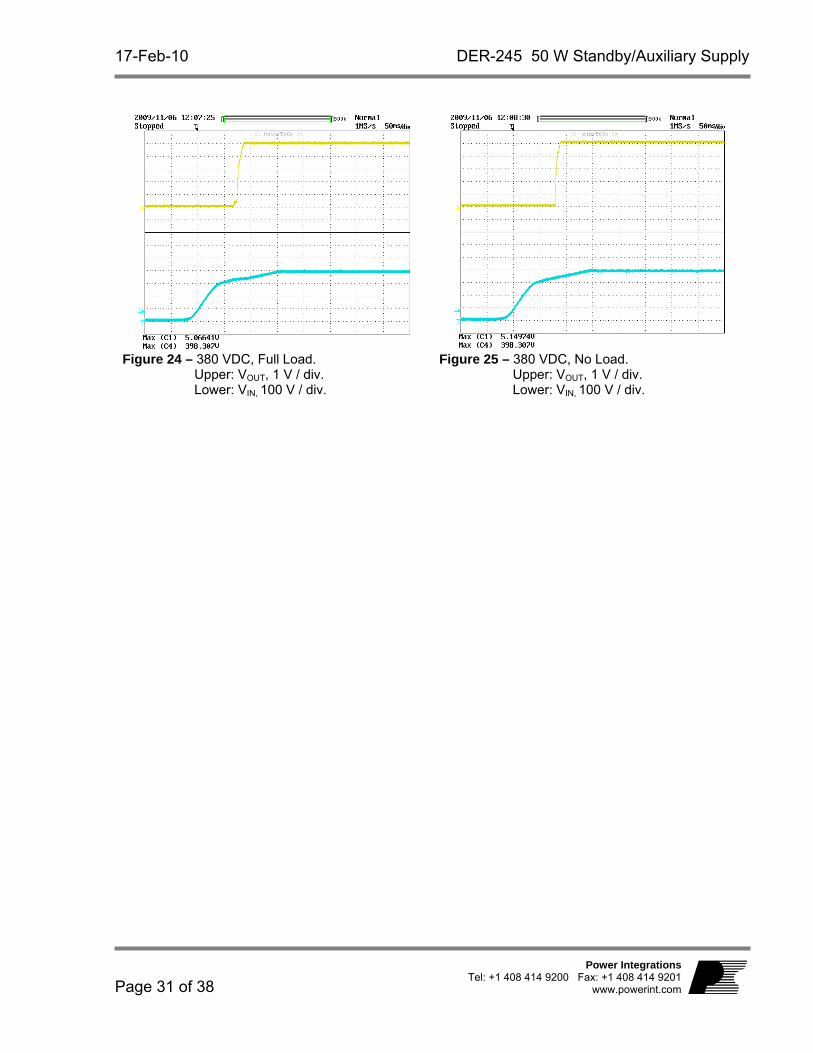
Figure 24 – 380 VDC, Full Load.
Upper: VOUT, 1 V / div. Lower: VIN, 100 V / div.
Figure 25 – 380 VDC, No Load. Upper: VOUT, 1 V / div. Lower: VIN, 100 V / div.

DER-245 50 W Standby/Auxiliary Supply 17-Feb-10
Page 32 of 38
Power Integrations, Inc. Tel: +1 408 414 9200 Fax: +1 408 414 9201 www.powerint.com
11.3 Drain Voltage and Current Start-up Profile
Figure 26 – 264 VAC, Full Load Start-up.
Upper: VOUT, 1 V / div. Lower: VDRAIN, 100 V / div.
Figure 27 – 264 VAC, Full Load Start-up. Upper: VOUT, 1 V / div. Lower: IDRAIN, .5 A / div.
Figure 28 – 380 VDC, Full Load Start-up.
Upper: VOUT, 1 V / div. Lower: VDRAIN, 100 V / div.
Figure 29 – 264 VAC, Full Load Start-up. Upper: VOUT, 1 V / div. Lower: IDRAIN, .5 A / div.
17-Feb-10 DER-245 50 W Standby/Auxiliary Supply
Page 33 of 38
Power Integrations Tel: +1 408 414 9200 Fax: +1 408 414 9201
www.powerint.com
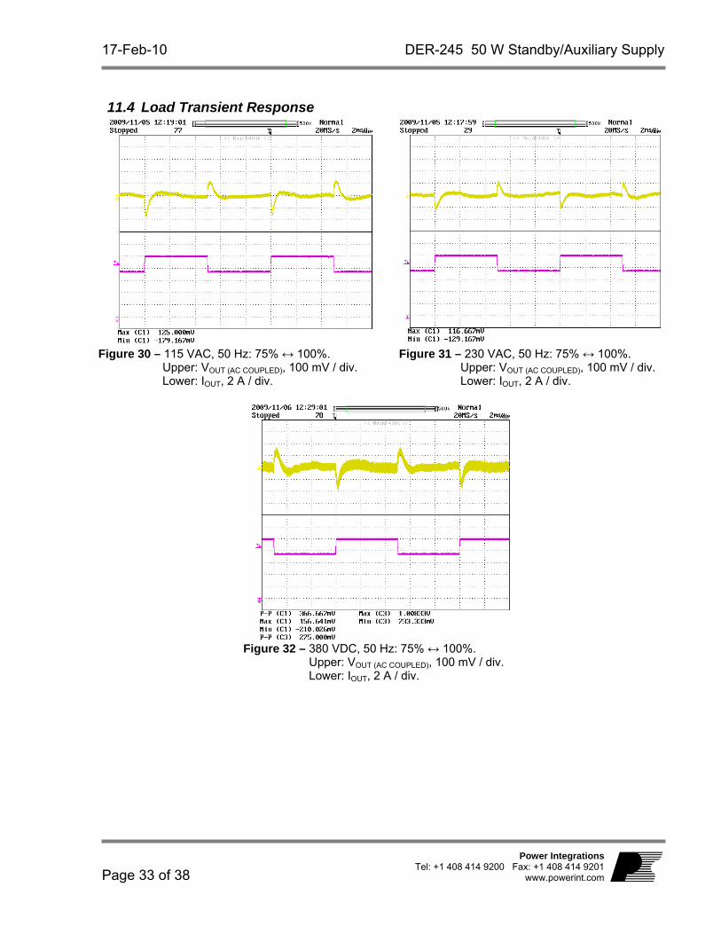
11.4 Load Transient Response
Figure 30 – 115 VAC, 50 Hz: 75% ↔ 100%.
Upper: VOUT (AC COUPLED), 100 mV / div. Lower: IOUT, 2 A / div.
Figure 31 – 230 VAC, 50 Hz: 75% ↔ 100%. Upper: VOUT (AC COUPLED), 100 mV / div. Lower: IOUT, 2 A / div.
Figure 32 – 380 VDC, 50 Hz: 75% ↔ 100%.
Upper: VOUT (AC COUPLED), 100 mV / div. Lower: IOUT, 2 A / div.

DER-245 50 W Standby/Auxiliary Supply 17-Feb-10
Page 34 of 38
Power Integrations, Inc. Tel: +1 408 414 9200 Fax: +1 408 414 9201 www.powerint.com
11.5 Output Ripple Measurements
11.5.1 Ripple Measurement Technique
For DC output ripple measurements, a modified oscilloscope test probe must be utilized in order to reduce spurious signals due to pickup. Details of the probe modification are provided in the figures below. The 4987BA probe adapter is affixed with two capacitors tied in parallel across the probe tip. The capacitors include one (1) 0.1 F/50 V ceramic type and one (1) 1.0 F / 50 V aluminum electrolytic. The aluminum electrolytic type capacitor is polarized, so proper polarity across DC outputs must be maintained (see below).
Figure 33 – Oscilloscope Probe Prepared for Ripple Measurement. (End Cap and Ground Lead Removed)
Figure 34 – Oscilloscope Probe with Probe Master (www.probemaster.com) 4987A BNC Adapter.
(Modified with wires for ripple measurement, and two parallel decoupling capacitors added)
Probe Ground
Probe Tip

17-Feb-10 DER-245 50 W Standby/Auxiliary Supply
Page 35 of 38
Power Integrations Tel: +1 408 414 9200 Fax: +1 408 414 9201
www.powerint.com
11.5.2 Measurement Results
Figure 35 – 115 VAC: 5 s / div. Figure 36 – 115 VAC: 5 ms / div.
Figure 37 – 230 VAC: 5 s / div. Figure 38 – 230 VAC: 5 ms / div.
Figure 39 – 380 VDC: 5 s / div. Figure 40 – 380 VDC: 5 ms / div.

DER-245 50 W Standby/Auxiliary Supply 17-Feb-10
Page 36 of 38
Power Integrations, Inc. Tel: +1 408 414 9200 Fax: +1 408 414 9201 www.powerint.com
12 Control Loop Measurements
12.1 115 VAC
Figure 41 – Gain-Phase Plot, 115 VAC, Maximum Steady State Load.
Vertical Scale: Gain = 10 dB / div., Phase = 30 °/ div. Crossover Frequency = 2.51 kHz, Phase Margin = 75.
12.2 230 VAC
Figure 42 – Gain-Phase Plot, 230 VAC, Maximum Steady State Load.
Vertical Scale: Gain = 10 dB / div., Phase = 30 °/ div. Crossover Frequency = 3.17 kHz, Phase Margin = 63.9.
17-Feb-10 DER-245 50 W Standby/Auxiliary Supply
Page 37 of 38
Power Integrations Tel: +1 408 414 9200 Fax: +1 408 414 9201
www.powerint.com
13 Revision History Date Author Revision Description & changes Reviewed
17-Feb-10 CA 1.0 Initial release Apps & Mktg

DER-245 50 W Standby/Auxiliary Supply 17-Feb-10
Page 38 of 38
Power Integrations, Inc. Tel: +1 408 414 9200 Fax: +1 408 414 9201 www.powerint.com
For the latest updates, visit our website: www.powerint.com Power Integrations reserves the right to make changes to its products at any time to improve reliability or manufacturability. Power Integrations does not assume any liability arising from the use of any device or circuit described herein. POWER INTEGRATIONS MAKES NO WARRANTY HEREIN AND SPECIFICALLY DISCLAIMS ALL WARRANTIES INCLUDING, WITHOUT LIMITATION, THE IMPLIED WARRANTIES OF MERCHANTABILITY, FITNESS FOR A PARTICULAR PURPOSE, AND NON-INFRINGEMENT OF THIRD PARTY RIGHTS.
PATENT INFORMATION The products and applications illustrated herein (including transformer construction and circuits external to the products) may be covered by one or more U.S. and foreign patents, or potentially by pending U.S. and foreign patent applications assigned to Power Integrations. A complete list of Power Integrations’ patents may be found at www.powerint.com. Power Integrations grants its customers a license under certain patent rights as set forth at http://www.powerint.com/ip.htm. The PI Logo, TOPSwitch, TinySwitch, LinkSwitch, DPA-Switch, PeakSwitch, EcoSmart, Clampless, E-Shield, Filterfuse, StackFET, PI Expert and PI FACTS are trademarks of Power Integrations, Inc. Other trademarks are property of their respective companies. ©Copyright 2010 Power Integrations, Inc.
Power Integrations Worldwide Sales Support Locations
WORLD HEADQUARTERS 5245 Hellyer Avenue San Jose, CA 95138, USA. Main: +1-408-414-9200 Customer Service: Phone: +1-408-414-9665 Fax: +1-408-414-9765 e-mail: [email protected]
GERMANY Rueckertstrasse 3 D-80336, Munich Germany Phone: +49-89-5527-3911 Fax: +49-89-5527-3920 e-mail: [email protected]
JAPAN Kosei Dai-3 Building 2-12-11, Shin-Yokohama, Kohoku-ku, Yokohama-shi, Kanagawa 222-0033 Japan Phone: +81-45-471-1021 Fax: +81-45-471-3717 e-mail: [email protected]
TAIWAN 5F, No. 318, Nei Hu Rd., Sec. 1 Nei Hu District Taipei 114, Taiwan R.O.C. Phone: +886-2-2659-4570 Fax: +886-2-2659-4550 e-mail: [email protected]
CHINA (SHANGHAI) Rm 1601/1610, Tower 1 Kerry Everbright City No. 218 Tianmu Road West Shanghai, P.R.C. 200070 Phone: +86-021-6354-6323 Fax: +86-021-6354-6325 e-mail: [email protected]
INDIA #1, 14th Main Road Vasanthanagar Bangalore-560052 India Phone: +91-80-4113-8020 Fax: +91-80-4113-8023 e-mail: [email protected]
KOREA RM 602, 6FL Korea City Air Terminal B/D, 159-6 Samsung-Dong, Kangnam-Gu, Seoul, 135-728 Korea Phone: +82-2-2016-6610 Fax: +82-2-2016-6630 e-mail: [email protected]
UNITED KINGDOM 1st Floor, St. James’s House East Street, Farnham Surrey, GU9 7TJ United Kingdom Phone: +44 (0) 1252-730-141 Fax: +44 (0) 1252-727-689 e-mail: [email protected]
CHINA (SHENZHEN) Rm A, B & C 4th Floor, Block C, Electronics Science and Technology Building 2070 Shennan Zhong Road Shenzhen, Guangdong, P.R.C. 518031 Phone: +86-755-8379-3243 Fax: +86-755-8379-5828 e-mail: [email protected]
ITALY Via De Amicis 2 20091 Bresso MI Italy Phone: +39-028-928-6000 Fax: +39-028-928-6009 e-mail: [email protected]
SINGAPORE 51 Newton Road, #15-08/10 Goldhill Plaza Singapore, 308900 Phone: +65-6358-2160 Fax: +65-6358-2015 e-mail: [email protected]
APPLICATIONS HOTLINE World Wide +1-408-414-9660 APPLICATIONS FAX World Wide +1-408-414-9760
Recommended