Power Integrations 5245 Hellyer Avenue, San Jose, CA 95138 USA.
Tel: +1 408 414 9200 Fax: +1 408 414 9201 www.power.com
Design Example Report
Title 35 W High Power Factor Isolated Flyback with Switched Valley Fill PFC Power Supply Using LYTSwitchTM-6 LYT6068C
Specification 140 VAC – 320 VAC Input; 12 V, 2.92 A Output
Application Emergency Light with Battery Charging
Author Applications Engineering Department
Document Number
DER-637
Date April 23, 2018
Revision 1.4
Summary and Features
Accurate constant voltage regulation High power factor, >0.9 at 230 V and 277 V inputs Fast transient load response Highly energy efficient, >88 % at 230 V and 277 V inputs Integrated protection and reliability features
Output short-circuit protection Line and output OVP Thermal foldback and over-temperature shutdown with hysteretic automatic power
recovery
No damage during line brown-out or brown-in conditions Meets IEC 2.5 kV ring wave, 1 kV differential surge Meets EN55015 conducted EMI
PATENT INFORMATION The products and applications illustrated herein (including transformer construction and circuits external to the products) may be covered by one or more U.S. and foreign patents, or potentially by pending U.S. and foreign patent applications assigned to Power Integrations. A complete list of Power Integrations' patents may be found at www.powerint.com. Power Integrations grants its customers a license under certain patent rights as set forth at <http://www.powerint.com/ip.htm>.
DER-637 35 W High PF Isolated Flyback using LYTSwitch-6 23-Apr-18
Page 2 of 84
Power Integrations, Inc. Tel: +1 408 414 9200 Fax: +1 408 414 9201 www.power.com
Table of Contents 1 Introduction ......................................................................................................... 4
2 Power Supply Specification ................................................................................... 6
3 Schematic ............................................................................................................ 7
4 Circuit Description ................................................................................................ 8
4.1 Input EMI Filter and Rectifier .......................................................................... 8
4.2 LYTSwitch-6 Primary Side Control ................................................................... 8
4.3 LYTSwitch-6 Secondary-Side Control ............................................................... 9
4.4 PFC Circuit Operation ................................................................................... 10
5 PCB Layout ........................................................................................................ 12
6 Bill of Materials .................................................................................................. 13
6.1 Main Bill of Material ..................................................................................... 13
6.2 Miscellaneous Parts ...................................................................................... 14
7 Flyback Transformer (T1) Specification ................................................................ 15
7.1 Electrical Diagram ........................................................................................ 15
7.2 Electrical Specifications ................................................................................ 15
7.3 Material List ................................................................................................ 15
7.4 Transformer Build Diagram .......................................................................... 16
7.5 Transformer Construction ............................................................................. 16
7.6 Transformer Winding Illustrations ................................................................. 17
8 PFC Inductor (T2) Specifications ......................................................................... 22
8.1 Electrical Diagram ........................................................................................ 22
8.2 Electrical Specifications ................................................................................ 22
8.3 Material List ................................................................................................ 22
8.4 Inductor Build Diagram ................................................................................ 23
8.5 Inductor Construction .................................................................................. 23
8.6 Inductor Winding Illustrations ...................................................................... 24
9 Design Spreadsheet ............................................................................................ 26
10 Performance Data ........................................................................................... 30
10.1 Output Voltage Regulation ........................................................................... 30
10.2 System Efficiency ......................................................................................... 31
10.3 Power Factor ............................................................................................... 32
10.4 %ATHD ...................................................................................................... 33
10.5 Individual Harmonics Content at Full Load ..................................................... 34
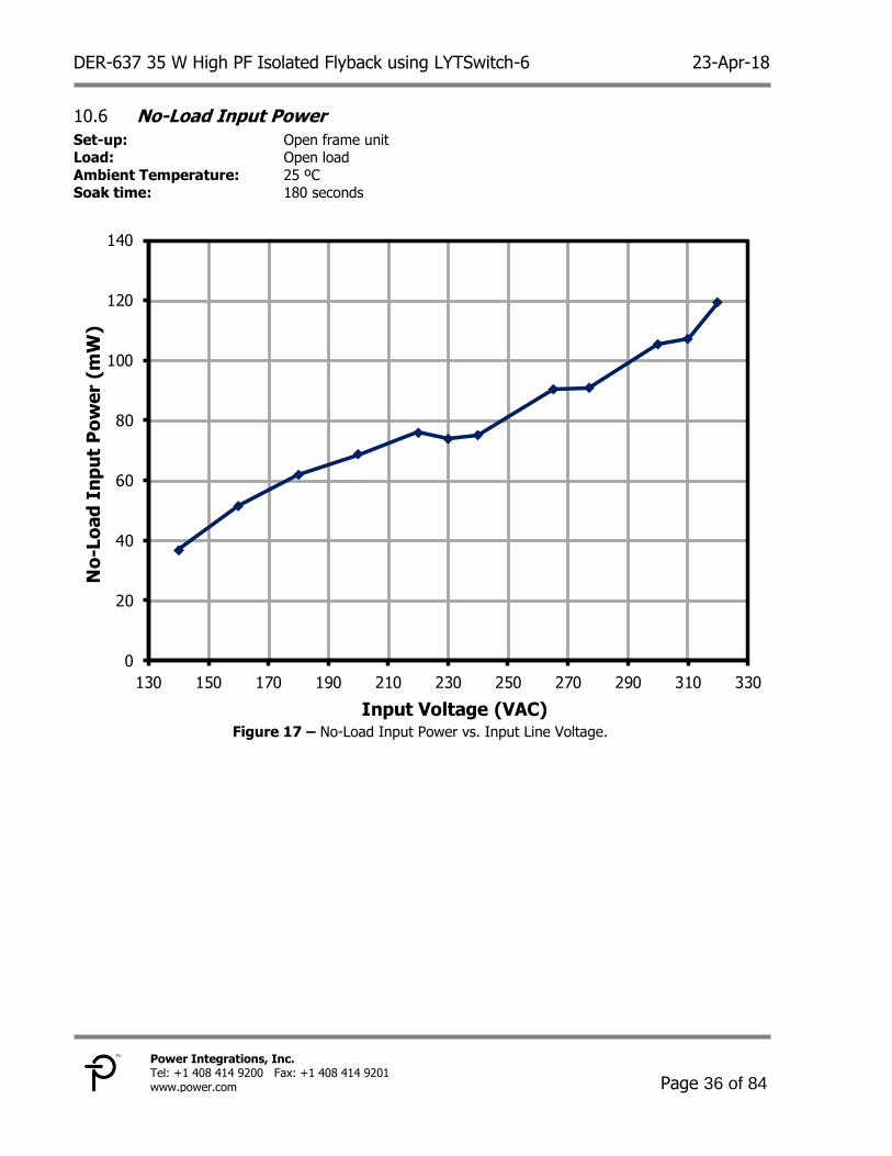
10.6 No-Load Input Power ................................................................................... 36
10.7 CV/CC Curve ............................................................................................... 37
11 Test Data ....................................................................................................... 38
11.1 Test Data at Full Load .................................................................................. 38
11.2 Test Data at No-Load ................................................................................... 38
11.3 Individual Harmonic Content at 230 VAC 50 Hz and Full Load ......................... 39
11.4 Individual Harmonic Content at 277 VAC 50 Hz and Full Load ......................... 40
12 Load Regulation Performance .......................................................................... 41
12.1 Output Voltage Load Regulation ................................................................... 41
23-Apr-18 DER-637 35 W High PF Isolated Flyback using LYTSwitch-6
Page 3 of 84
Power Integrations Tel: +1 408 414 9200 Fax: +1 408 414 9201
www.power.com
12.2 Efficiency vs. Load ....................................................................................... 42
12.3 Average Efficiency ....................................................................................... 42
Average Efficiency Measurement ............................................................ 42 12.3.112.4 Power Factor vs. Load .................................................................................. 43
12.5 %ATHD vs. Load ......................................................................................... 44
13 Thermal Performance ...................................................................................... 45
13.1 Thermal Measurements at Room Temp Ambient ............................................ 45
13.2 Thermal Performance at High Temp Ambient ................................................ 47
14 Waveforms ..................................................................................................... 49
14.1 Input Voltage and Input Current at Full Load ................................................. 49
14.2 Start-up Profile at Full Load .......................................................................... 50
14.3 Output Voltage Fall ...................................................................................... 51
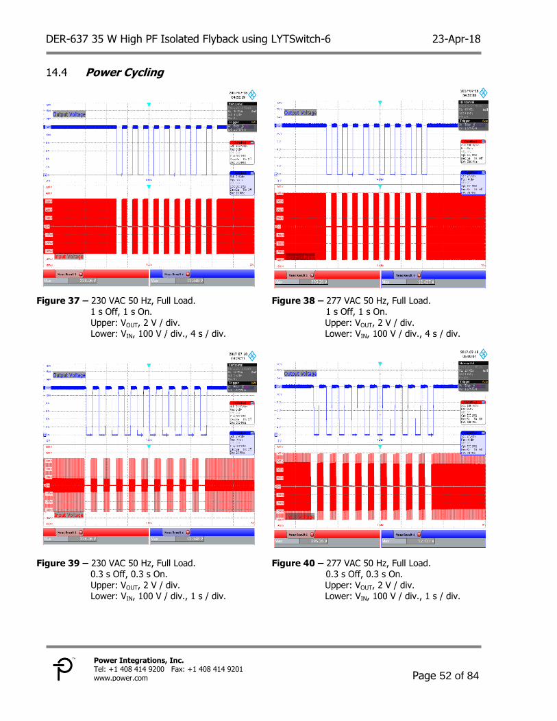
14.4 Power Cycling .............................................................................................. 52
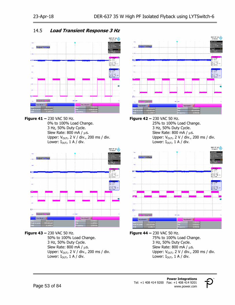
14.5 Load Transient Response 3 Hz ...................................................................... 53
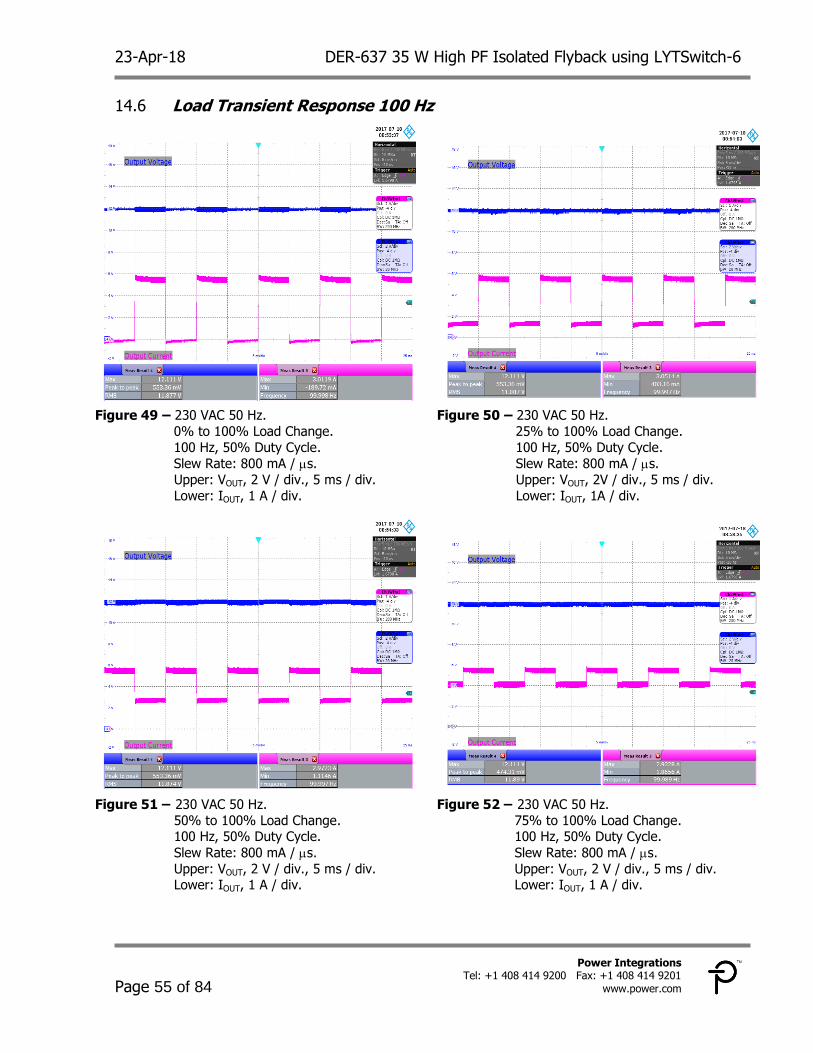
14.6 Load Transient Response 100 Hz .................................................................. 55
14.7 LYTSwitch-6 Drain Voltage and Current Waveforms at Normal Operation ........ 57
14.8 LYTSwitch-6 Drain Voltage and Current at Full Load Start-up ......................... 60
14.9 LYTSwitch-6 Drain Voltage and Current during Output Short-Circuit ................ 62
14.10 PFC Diode Voltage and Current at Normal Operation .................................. 64
14.11 PFC Diode Voltage and Current at Start-up Full Load .................................. 65
14.12 SR FET Drain Voltage and Current at Normal Operation .............................. 66
14.13 SR FET Drain Voltage and Current at Full Load Start-up .............................. 68
14.14 Output Voltage Ripple ............................................................................... 70
14.15 Output Current Ripple ............................................................................... 73
Equipment Used ................................................................................ 73 14.15.1 Ripple Ratio and Flicker % Measurement ............................................ 73 14.15.2
15 Conducted EMI ............................................................................................... 75
15.1 Test Set-up ................................................................................................. 75
Equipment and Load Used ..................................................................... 75 15.1.115.2 EMI Test Result ........................................................................................... 76
16 Line Surge ...................................................................................................... 78
16.1 Differential Surge Test Results ...................................................................... 79
16.2 Ring Wave Surge Test Results ...................................................................... 79
16.3 1 kV Differential Surge Test .......................................................................... 80
16.4 2.5 kV Ring Wave Surge Test ....................................................................... 81
17 Brown-in / Brown-out Test .............................................................................. 82
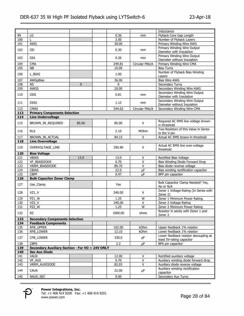
18 Revision History .............................................................................................. 83
Important Note: Although this board is designed to satisfy safety isolation requirements, the engineering prototype has not been agency approved. Therefore, all testing should be performed using an isolation
transformer to provide the AC input to the prototype board.
DER-637 35 W High PF Isolated Flyback using LYTSwitch-6 23-Apr-18
Page 4 of 84
Power Integrations, Inc. Tel: +1 408 414 9200 Fax: +1 408 414 9201 www.power.com
Introduction 1
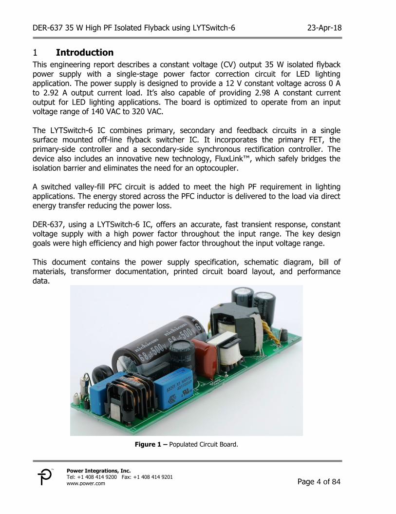
This engineering report describes a constant voltage (CV) output 35 W isolated flyback power supply with a single-stage power factor correction circuit for LED lighting application. The power supply is designed to provide a 12 V constant voltage across 0 A to 2.92 A output current load. It’s also capable of providing 2.98 A constant current output for LED lighting applications. The board is optimized to operate from an input voltage range of 140 VAC to 320 VAC. The LYTSwitch-6 IC combines primary, secondary and feedback circuits in a single surface mounted off-line flyback switcher IC. It incorporates the primary FET, the primary-side controller and a secondary-side synchronous rectification controller. The device also includes an innovative new technology, FluxLink™, which safely bridges the isolation barrier and eliminates the need for an optocoupler. A switched valley-fill PFC circuit is added to meet the high PF requirement in lighting applications. The energy stored across the PFC inductor is delivered to the load via direct energy transfer reducing the power loss. DER-637, using a LYTSwitch-6 IC, offers an accurate, fast transient response, constant voltage supply with a high power factor throughout the input range. The key design goals were high efficiency and high power factor throughout the input voltage range. This document contains the power supply specification, schematic diagram, bill of materials, transformer documentation, printed circuit board layout, and performance data.
Figure 1 – Populated Circuit Board.
23-Apr-18 DER-637 35 W High PF Isolated Flyback using LYTSwitch-6
Page 5 of 84
Power Integrations Tel: +1 408 414 9200 Fax: +1 408 414 9201
www.power.com
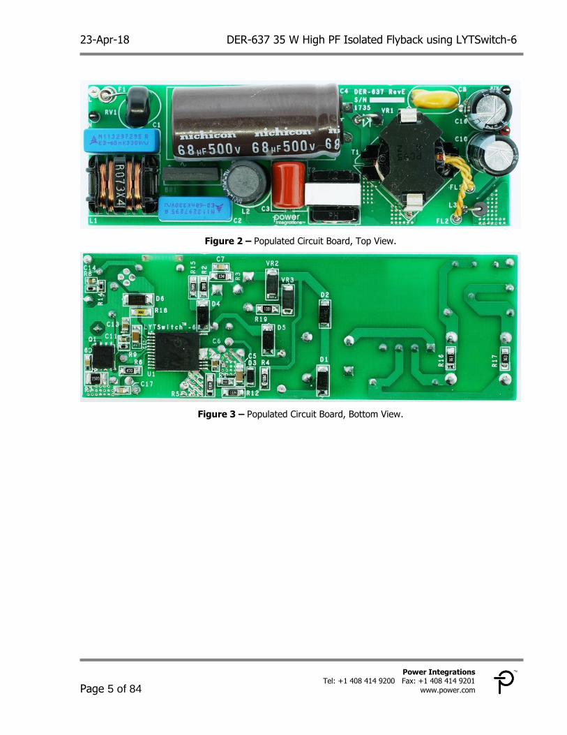
Figure 2 – Populated Circuit Board, Top View.
Figure 3 – Populated Circuit Board, Bottom View.
DER-637 35 W High PF Isolated Flyback using LYTSwitch-6 23-Apr-18
Page 6 of 84
Power Integrations, Inc. Tel: +1 408 414 9200 Fax: +1 408 414 9201 www.power.com
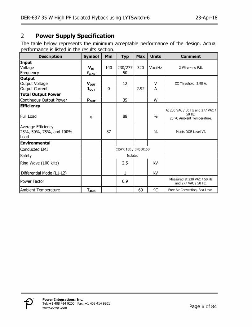
Power Supply Specification 2
The table below represents the minimum acceptable performance of the design. Actual performance is listed in the results section.
Description Symbol Min Typ Max Units Comment
Input
Voltage VIN 140 230/277 320 Vac/Hz 2 Wire – no P.E.
Frequency fLINE 50
Output
Output Voltage VOUT 12 V CC Threshold: 2.98 A.
Output Current IOUT 0 2.92 A
Total Output Power
Continuous Output Power POUT 35 W
Efficiency
Full Load 88 %
At 230 VAC / 50 Hz and 277 VAC / 50 Hz.
25 ºC Ambient Temperature.
Average Efficiency
25%, 50%, 75%, and 100% Load
87 % Meets DOE Level VI.
Environmental
Conducted EMI CISPR 15B / EN55015B
Safety Isolated
Ring Wave (100 kHz)
Differential Mode (L1-L2)
2.5
1
kV
kV
Power Factor 0.9 Measured at 230 VAC / 50 Hz and 277 VAC / 50 Hz.
Ambient Temperature TAMB 60 ºC Free Air Convection, Sea Level.
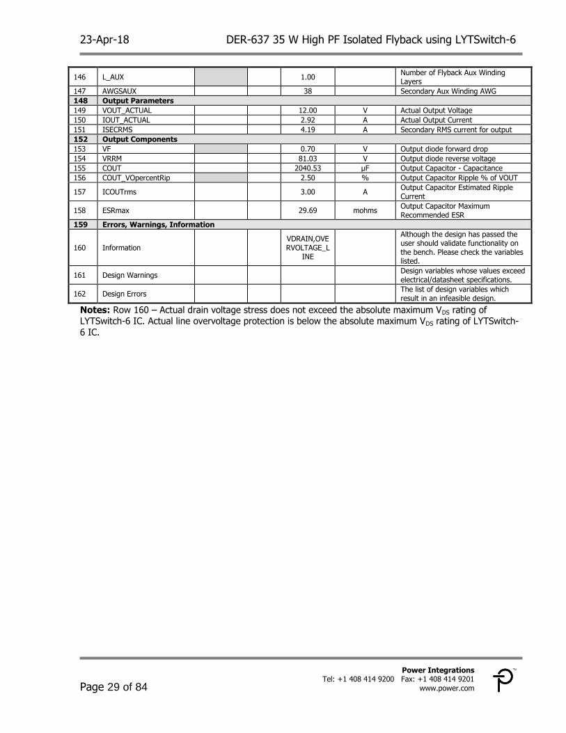
23-Apr-18 DER-637 35 W High PF Isolated Flyback using LYTSwitch-6
Page 7 of 84
Power Integrations Tel: +1 408 414 9200 Fax: +1 408 414 9201
www.power.com
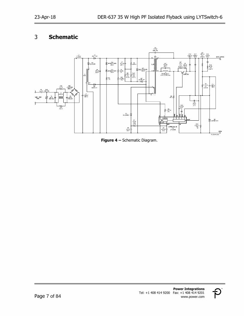
Schematic 3
Figure 4 – Schematic Diagram.
DER-637 35 W High PF Isolated Flyback using LYTSwitch-6 23-Apr-18
Page 8 of 84
Power Integrations, Inc. Tel: +1 408 414 9200 Fax: +1 408 414 9201 www.power.com
Circuit Description 4
The LYTSwitch-6 device (LYT6068C) incorporates the primary MOSFET, the primary-side controller and a secondary-side synchronous rectification controller in a single inSOP-24D package. This IC also includes an innovative new technology, FluxLink™, which safely bridges the isolation barrier and eliminates the need for an optocoupler. The LYTSwitch-6 IC is configured to drive a 35 W flyback power supply with a switched valley fill PFC providing a high power factor 12 V constant voltage supply throughout the input range of 140 VAC to 320 VAC.
Input EMI Filter and Rectifier 4.1
The input fuse F1 provides safety protection from component failures. Varistor RV1 acts as a voltage clamp that limits the voltage spike on the primary during line transient voltage surge events. A 350 V rated part was selected, being slightly above the maximum specified operating input voltage (320 V). The AC input voltage is full wave rectified by BR1 to achieve good power factor and low THD. The bulk capacitor (C4) provides input line ripple voltage filtering for a stable flyback DC supply voltage and helps reduce EMI noise. It also stores excess energy generated by the PFC during the power switch turn off time. Capacitor C1, L1, C2, L2, and C3 forms a 2 stage LC EMI filter to suppress differential mode noise caused by the PFC and flyback switching action. Common mode noise is suppressed by Y capacitor C8. Rectifier diode (D2) provides a bypass charging current to the bulk capacitor (C4) from the input rectified voltage. Diode D2 also serves as a blocking diode during the power MOSFET turn OFF to isolate the flyback DC supply from the PFC supply maintaining the functionality of the added PFC circuit.
LYTSwitch-6 Primary Side Control 4.2
The isolated flyback power supply is controlled by the LYTSwitch-6 IC LYT6068C. One side of the transformer (T1) primary is connected to the positive output terminal of the bulk capacitor (C4) while the other side is connected to the drain of the integrated 650 V power MOSFET inside the LYTSwitch-6 IC (U1). A low cost RCDZ snubber clamp formed by D4, R2, R15, C7, R3, and VR1 limits the peak Drain voltage spike due to the effects of transformer leakage inductance. The VOLTAGE MONITOR (V) pin of the LYTSwitch-6 IC is connected to the positive of the bulk capacitor (C4) to provide input voltage information. The voltage across the bulk capacitor (C4) is sensed and converted into current through V pin resistors R4, R12, and R5 to provide detection of overvoltage. The IOV- determines the input overvoltage threshold.
23-Apr-18 DER-637 35 W High PF Isolated Flyback using LYTSwitch-6
Page 9 of 84
Power Integrations Tel: +1 408 414 9200 Fax: +1 408 414 9201
www.power.com
During the initial power-up, the internal high-voltage current source charges the BPP pin capacitor (C6). Before switching, the primary will pause for around 80 ms to listen for secondary request signals. When the primary starts switching after initial power-up, it will initially assume control and require a handshake to pass the control to the secondary side. The LYTSwitch-6 IC is at normal operation when switching with the secondary in control. During normal operation the primary-side block is powered by the auxiliary winding of the transformer. The output of this is configured as a flyback winding, rectified and filtered (D3 and C5) and fed to the BPP pin via a current limiting resistor R1. The value of the BPP pin capacitor C6 sets the current limit of the LYTSwitch-6 IC. The 0.47 F capacitance value for C6 corresponds to STANDARD current limit mode.
The thermal shutdown circuitry senses the primary MOSFET die temperature. The threshold (TSD) is typically set to 142 °C with 70 °C hysteresis TSD(H). When the die temperature rises above this threshold the power MOSFET is disabled and remains disabled until the die temperature falls by TSD(H) at which point it is re-enabled. A large hysteresis of 70 °C is provided to prevent over-heating of the PCB due to continuous fault condition.
LYTSwitch-6 Secondary-Side Control 4.3
The secondary-side control of the LYTSwitch-6 IC provides output voltage and output current sensing. The secondary of the transformer is rectified by a synchronous rectifier MOSFET (Q1), driven by the Synchronous Rectifier Drive (SR) pin of LYTSwitch-6 IC. This is then filtered by the output capacitors C10 and C16. Adding an RC snubber (R7 and C9) across the SR FET reduces voltage stress across its drain-to-source. An LC filter (L3 and C17) in series with the secondary winding of the transformer helps to further reduce the voltage spike across the drain-to-source of the SR FET, if a simple RC snubber is not enough, with little to no effect on system efficiency. Component L3 is a single-turn ferrite bead that, in conjunction with a parallel ceramic capacitor C17, suppresses high frequency spike present on the secondary of the transformer especially during start-up. The secondary side of the IC is self-powered from either the secondary bias winding forward voltage or the 12 V regulated output. During normal operation the regulated output voltage powers the device, through the OUTPUT VOLTAGE (VOUT) pin. During start-up operation, when the output voltage is still building-up, the device will power itself from the secondary winding directly. During the ON-time of the primary-side MOSFET the forward voltage that appears across the secondary winding is used to charge the (BPS) capacitor C12 via the FORWARD (FWD) pin through resistor R6 and an internal regulator. During constant voltage mode operation, output voltage regulation is achieved through sensing the output voltage via divider resistors R8 and R9. The voltage across R9 is fed into the FB pin with an internal reference voltage threshold of 1.265 V. Filter capacitor
DER-637 35 W High PF Isolated Flyback using LYTSwitch-6 23-Apr-18
Page 10 of 84
Power Integrations, Inc. Tel: +1 408 414 9200 Fax: +1 408 414 9201 www.power.com
C11 is added across R9 to eliminate unwanted noise that might trigger the OVP function or increase the output ripple voltage. The feedforward network composed of C14 and R14 across R8 helps reduce output voltage ripple and achieve better output voltage regulation. Capacitor C13 filters out any unwanted noise that may enter the VOUT pin, and also helps reduce output voltage ripple. During constant current operation, the output current is set by the sense resistor (R18) across the IS pin and the GND pin. The internal reference threshold for the IS pin is 35.8 mV. Diode D6 in parallel with the current sense resistor serves as protection during output short-circuit conditions. The thermal foldback is activated when the secondary controller die temperature reaches 124 °C, the output power is reduced by reducing the constant current reference threshold.
PFC Circuit Operation 4.4
Without the added PFC circuit, the power factor of the flyback power supply is normally around 0.5 to 0.6 at full load condition. The input of the flyback power supply circuit usually consists of the full wave bridge rectifier (BR1) followed by a storage bulk capacitor (C4) capable of maintaining a voltage approximately equal to the peak voltage of the input sine wave until the next peak comes to recharge the capacitor. The input charging pulse current must be high enough to sustain the load until the next peak. This means that the charging pulse current is around 5-10 times higher than the average current with a high phase angle difference from the voltage waveform; hence, the expected PF from this standard configuration is low and THD is high. The added PFC circuit is called “Switched Valley-Fill Single Stage PFC” (SVF S2PFC). It is comprised of an inductor (T2) and diodes (D1 and D5) connected directly to the DRAIN pin of the LYTSwitch-6 IC. The LYTSwitch-6 flyback switching action is able to draw a high frequency pulse current from the full wave rectified input. This will reduce the rms input current and the phase angle difference from the input line voltage will be lower; hence, power factor will increase and will improve THD. The PFC inductor T2 operates in DCM mode. During the LYTSwitch-6 turn ON time, current drawn from the rectified input ramps through the PFC inductor (T2) storing energy. The stored energy on T2 is then delivered to the load via direct energy transfer between the primary and secondary winding of the flyback transformer T1. Any excess energy from the PFC inductor that is not delivered to the load is being stored to the bulk capacitor. During no-load and light load conditions (i.e, less than 250 mA output load current), the secondary requires less energy from the primary; therefore, more excess energy from the PFC inductor is stored on the bulk capacitor causing the voltage to rise gradually. The expected voltage stress across the bulk capacitor C4 will be higher than the peak input voltage. To limit the bulk voltage below the bulk capacitor rating, especially at high input voltage, a Zener-resistor clamp circuit is used (VR2, VR3, and
23-Apr-18 DER-637 35 W High PF Isolated Flyback using LYTSwitch-6
Page 11 of 84
Power Integrations Tel: +1 408 414 9200 Fax: +1 408 414 9201
www.power.com
R19). The Zener voltage is set at 480 V; when the bulk voltage goes beyond this, the Zener diodes conduct and bleed current from the bulk capacitor through resistor R19. This prevents the bulk capacitor voltage to rise above 480 V. The power dissipation of this Zener-resistor clamp should be considered at the worst-case creeping of the bulk voltage – happens usually at light load condition. Diodes D1 and D5 are connected in series to withstand voltage stress caused by the resonance ringing during the FET turn off. The variability of the PFC inductor peak current will be compensated by LYTSwitch-6 primary and secondary side control maintaining the voltage regulation at all conditions. A low cost RCD clamp circuit across the Drain-to-Source pins of the LYTSwitch-6 IC will also limit the bulk voltage from rising at light load, but the additional dissipation will cause a decrease in overall system efficiency and increase no-load input power consumption.
DER-637 35 W High PF Isolated Flyback using LYTSwitch-6 23-Apr-18
Page 12 of 84
Power Integrations, Inc. Tel: +1 408 414 9200 Fax: +1 408 414 9201 www.power.com
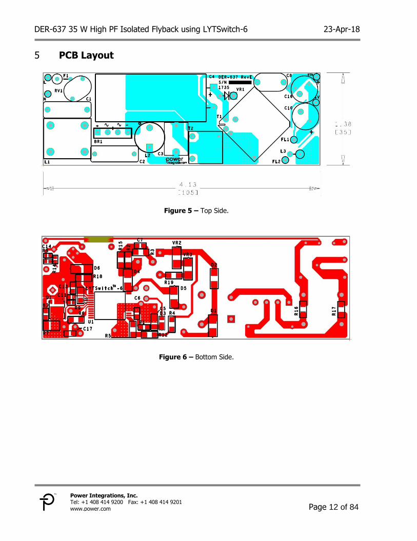
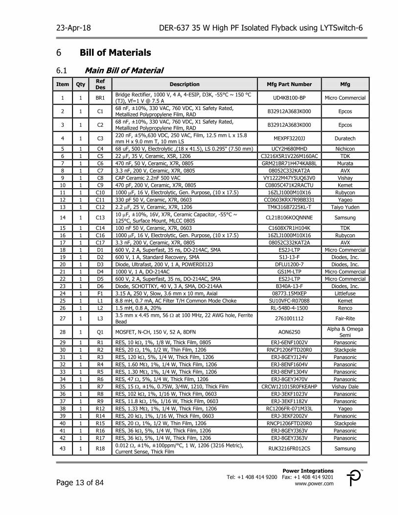
PCB Layout 5
Figure 5 – Top Side.
Figure 6 – Bottom Side.
23-Apr-18 DER-637 35 W High PF Isolated Flyback using LYTSwitch-6
Page 13 of 84
Power Integrations Tel: +1 408 414 9200 Fax: +1 408 414 9201
www.power.com
Bill of Materials 6
Main Bill of Material 6.1
Item Qty Ref Des
Description Mfg Part Number Mfg
1 1 BR1 Bridge Rectifier, 1000 V, 4 A, 4-ESIP, D3K, -55°C ~ 150 °C (TJ), Vf=1 V @ 7.5 A
UD4KB100-BP Micro Commercial
2 1 C1 68 nF, ±10%, 330 VAC, 760 VDC, X1 Safety Rated, Metallized Polypropylene Film, RAD
B32912A3683K000 Epcos
3 1 C2 68 nF, ±10%, 330 VAC, 760 VDC, X1 Safety Rated, Metallized Polypropylene Film, RAD
B32912A3683K000 Epcos
4 1 C3 220 nF, ±5%,630 VDC, 250 VAC, Film, 12.5 mm L x 15.8 mm H x 9.0 mm T, 10 mm LS
MEXPF3220JJ Duratech
5 1 C4 68 uF, 500 V, Electrolytic ,(18 x 41.5), LS 0.295" (7.50 mm) UCY2H680MHD Nichicon
6 1 C5 22 F, 35 V, Ceramic, X5R, 1206 C3216X5R1V226M160AC TDK
7 1 C6 470 nF, 50 V, Ceramic, X7R, 0805 GRM21BR71H474KA88L Murata
8 1 C7 3.3 nF, 200 V, Ceramic, X7R, 0805 08052C332KAT2A AVX
9 1 C8 CAP Ceramic 2.2nF 500 VAC VY1222M47Y5UQ63V0 Vishay
10 1 C9 470 pF, 200 V, Ceramic, X7R, 0805 C0805C471K2RACTU Kemet
11 1 C10 1000 F, 16 V, Electrolytic, Gen. Purpose, (10 x 17.5) 16ZLJ1000M10X16 Rubycon
12 1 C11 330 pF 50 V, Ceramic, X7R, 0603 CC0603KRX7R9BB331 Yageo
13 1 C12 2.2 F, 25 V, Ceramic, X7R, 1206 TMK316B7225KL-T Taiyo Yuden
14 1 C13 10 F, ±10%, 16V, X7R, Ceramic Capacitor, -55°C ~ 125°C, Surface Mount, MLCC 0805
CL21B106KOQNNNE Samsung
15 1 C14 100 nF 50 V, Ceramic, X7R, 0603 C1608X7R1H104K TDK
16 1 C16 1000 F, 16 V, Electrolytic, Gen. Purpose, (10 x 17.5) 16ZLJ1000M10X16 Rubycon
17 1 C17 3.3 nF, 200 V, Ceramic, X7R, 0805 08052C332KAT2A AVX
18 1 D1 600 V, 2 A, Superfast, 35 ns, DO-214AC, SMA ES2J-LTP Micro Commercial
19 1 D2 600 V, 1 A, Standard Recovery, SMA S1J-13-F Diodes, Inc.
20 1 D3 Diode, Ultrafast, 200 V, 1 A, POWERDI123 DFLU1200-7 Diodes, Inc.
21 1 D4 1000 V, 1 A, DO-214AC GS1M-LTP Micro Commercial
22 1 D5 600 V, 2 A, Superfast, 35 ns, DO-214AC, SMA ES2J-LTP Micro Commercial
23 1 D6 Diode, SCHOTTKY, 40 V, 3 A, SMA, DO-214AA B340A-13-F Diodes, Inc.
24 1 F1 3.15 A, 250 V, Slow, 3.6 mm x 10 mm, Axial 08773.15MXEP Littlefuse
25 1 L1 8.8 mH, 0.7 mA, AC Filter T/H Common Mode Choke SU10VFC-R07088 Kemet
26 1 L2 1.5 mH, 0.8 A, 20% RL-5480-4-1500 Renco
27 1 L3 3.5 mm x 4.45 mm, 56 at 100 MHz, 22 AWG hole, Ferrite
Bead 2761001112 Fair-Rite
28 1 Q1 MOSFET, N-CH, 150 V, 52 A, 8DFN AON6250 Alpha & Omega
Semi
29 1 R1 RES, 10 k, 1%, 1/8 W, Thick Film, 0805 ERJ-6ENF1002V Panasonic
30 1 R2 RES, 20 , 1%, 1/2 W, Thin Film, 1206 RNCP1206FTD20R0 Stackpole
31 1 R3 RES, 120 k, 5%, 1/4 W, Thick Film, 1206 ERJ-8GEYJ124V Panasonic
32 1 R4 RES, 1.60 M, 1%, 1/4 W, Thick Film, 1206 ERJ-8ENF1604V Panasonic
33 1 R5 RES, 1.30 M, 1%, 1/4 W, Thick Film, 1206 ERJ-8ENF1304V Panasonic
34 1 R6 RES, 47 , 5%, 1/4 W, Thick Film, 1206 ERJ-8GEYJ470V Panasonic
35 1 R7 RES, 15 , ±1%, 0.75W, 3/4W, 1210, Thick Film CRCW121015R0FKEAHP Vishay Dale
36 1 R8 RES, 102 k, 1%, 1/16 W, Thick Film, 0603 ERJ-3EKF1023V Panasonic
37 1 R9 RES, 11.8 k, 1%, 1/16 W, Thick Film, 0603 ERJ-3EKF1182V Panasonic
38 1 R12 RES, 1.33 M, 1%, 1/4 W, Thick Film, 1206 RC1206FR-071M33L Yageo
39 1 R14 RES, 20 k, 1%, 1/16 W, Thick Film, 0603 ERJ-3EKF2002V Panasonic
40 1 R15 RES, 20 , 1%, 1/2 W, Thin Film, 1206 RNCP1206FTD20R0 Stackpole
41 1 R16 RES, 36 k, 5%, 1/4 W, Thick Film, 1206 ERJ-8GEYJ363V Panasonic
42 1 R17 RES, 36 k, 5%, 1/4 W, Thick Film, 1206 ERJ-8GEYJ363V Panasonic
43 1 R18 0.012 , ±1%, ±100ppm/°C, 1 W, 1206 (3216 Metric), Current Sense, Thick Film
RUK3216FR012CS Samsung
DER-637 35 W High PF Isolated Flyback using LYTSwitch-6 23-Apr-18
Page 14 of 84
Power Integrations, Inc. Tel: +1 408 414 9200 Fax: +1 408 414 9201 www.power.com
44 1 R19 RES, 1 k, 5%, 1/4 W, Thick Film, 1206 ERJ-8GEYJ102V Panasonic
45 1 RV1 Varistor, 350 VAC, 3.5K A, 10.5 mm, Bulk ZNR, ERZ-E, Surge Absorber
ERZ-E08A561 Panasonic
46 1 T1 Bobbin, RM8, Vertical, 12 pins BRM08-1112CP-W-P5.0 MH&W
47 1 T2 Bobbin, EE13, Vertical, 10 pins P-1302-2 Pin Shine
48 1 VR1 DIODE, ZENER, 140 V, ±5%,1.5 W, DO204AL, DO-204AL (DO-41)
Z4KE140A-E3/54 Vishay
49 1 VR2 240 V, 1.25 W, 600 W (Peak, non-repetitive),5%, DO214AC (SMA)
BZG03C240TR Vishay
50 1 VR3 240 V, 1.25 W, 600 W (Peak, non-repetitive),5%, DO214AC (SMA)
BZG03C240TR Vishay
51 1 U1 LYTSwitch-6, InSOP24D LYT6068C Power
Integrations
Miscellaneous Parts 6.2
Item Qty Ref Des
Description Mfg Part Number
Mfg
1 1 +V Test Point, RED, Miniature THRU-HOLE MOUNT 5000 Keystone
2 1 RTN Test Point, BLK, Miniature THRU-HOLE MOUNT 5001 Keystone
3 1 L Test Point, WHT, Miniature THRU-HOLE MOUNT 5002 Keystone
4 1 N Test Point, BLK, THRU-HOLE MOUNT 5011 Keystone
5 1 FL1 Flying Lead, Hole size 50mils N/A N/A
6 1 FL2 Flying Lead, Hole size 50mils N/A N/A
23-Apr-18 DER-637 35 W High PF Isolated Flyback using LYTSwitch-6
Page 15 of 84
Power Integrations Tel: +1 408 414 9200 Fax: +1 408 414 9201
www.power.com
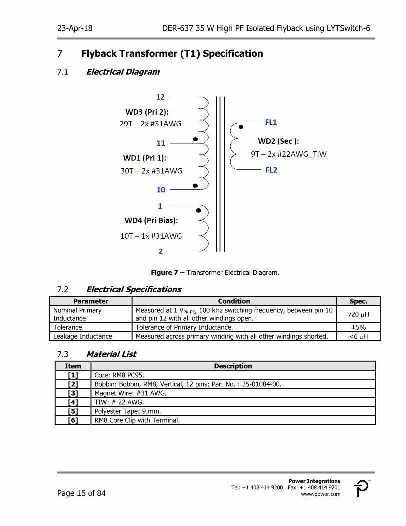
Flyback Transformer (T1) Specification 7
Electrical Diagram 7.1
Figure 7 – Transformer Electrical Diagram.
Electrical Specifications 7.2
Parameter Condition Spec.
Nominal Primary
Inductance
Measured at 1 VPK-PK, 100 kHz switching frequency, between pin 10
and pin 12 with all other windings open. 720 H
Tolerance Tolerance of Primary Inductance. ±5%
Leakage Inductance Measured across primary winding with all other windings shorted. <6 H
Material List 7.3
Item Description
[1] Core: RM8 PC95.
[2] Bobbin: Bobbin, RM8, Vertical, 12 pins; Part No. : 25-01084-00.
[3] Magnet Wire: #31 AWG.
[4] TIW: # 22 AWG.
[5] Polyester Tape: 9 mm.
[6] RM8 Core Clip with Terminal.
DER-637 35 W High PF Isolated Flyback using LYTSwitch-6 23-Apr-18
Page 16 of 84
Power Integrations, Inc. Tel: +1 408 414 9200 Fax: +1 408 414 9201 www.power.com
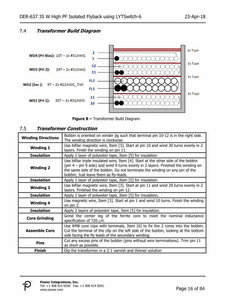
Transformer Build Diagram 7.4
Figure 8 – Transformer Build Diagram.
Transformer Construction 7.5
Winding Directions Bobbin is oriented on winder jig such that terminal pin 10-12 is in the right side.
The winding direction is clockwise.
Winding 1 Use bifilar magnetic wire, Item [3]. Start at pin 10 and wind 30 turns evenly in 2 layers. Finish the winding on pin 11.
Insulation Apply 1 layer of polyester tape, Item [5] for insulation
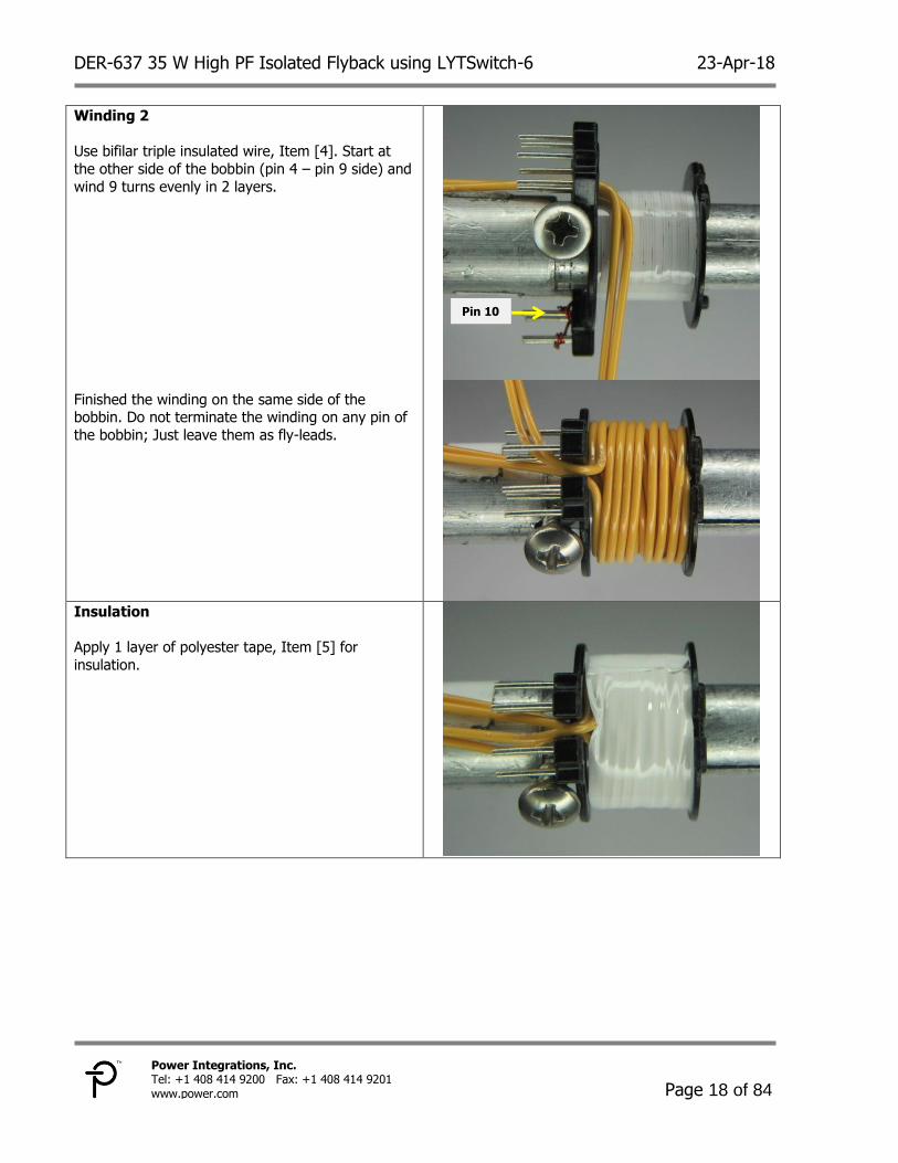
Winding 2
Use bifilar triple insulated wire, Item [4]. Start at the other side of the bobbin (pin 4 – pin 9 side) and wind 9 turns evenly in 2 layers. Finished the winding on
the same side of the bobbin. Do not terminate the winding on any pin of the bobbin; Just leave them as fly-leads.
Insulation Apply 1 layer of polyester tape, Item [5] for insulation.
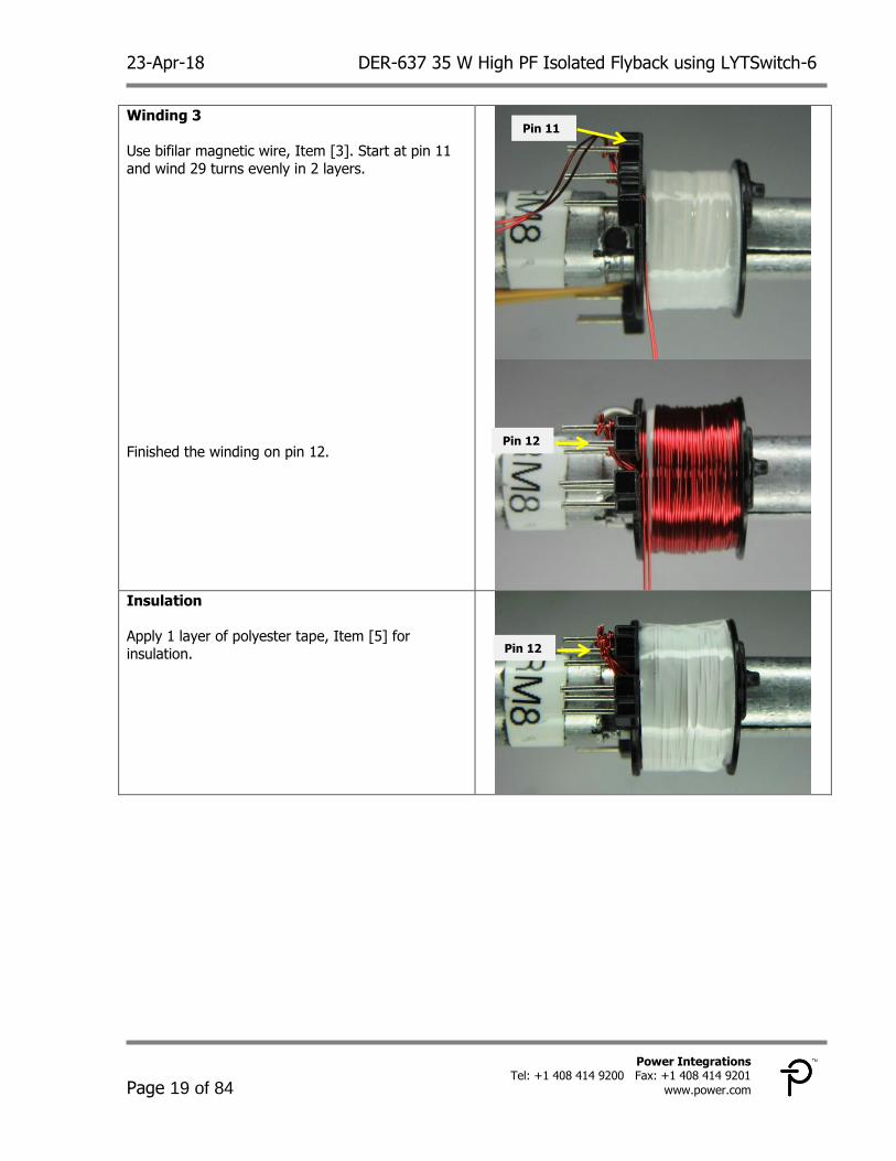
Winding 3 Use bifilar magnetic wire, Item [3]. Start at pin 11 and wind 29 turns evenly in 2 layers. Finished the winding on pin 12.
Insulation Apply 1 layer of polyester tape, Item [5] for insulation.
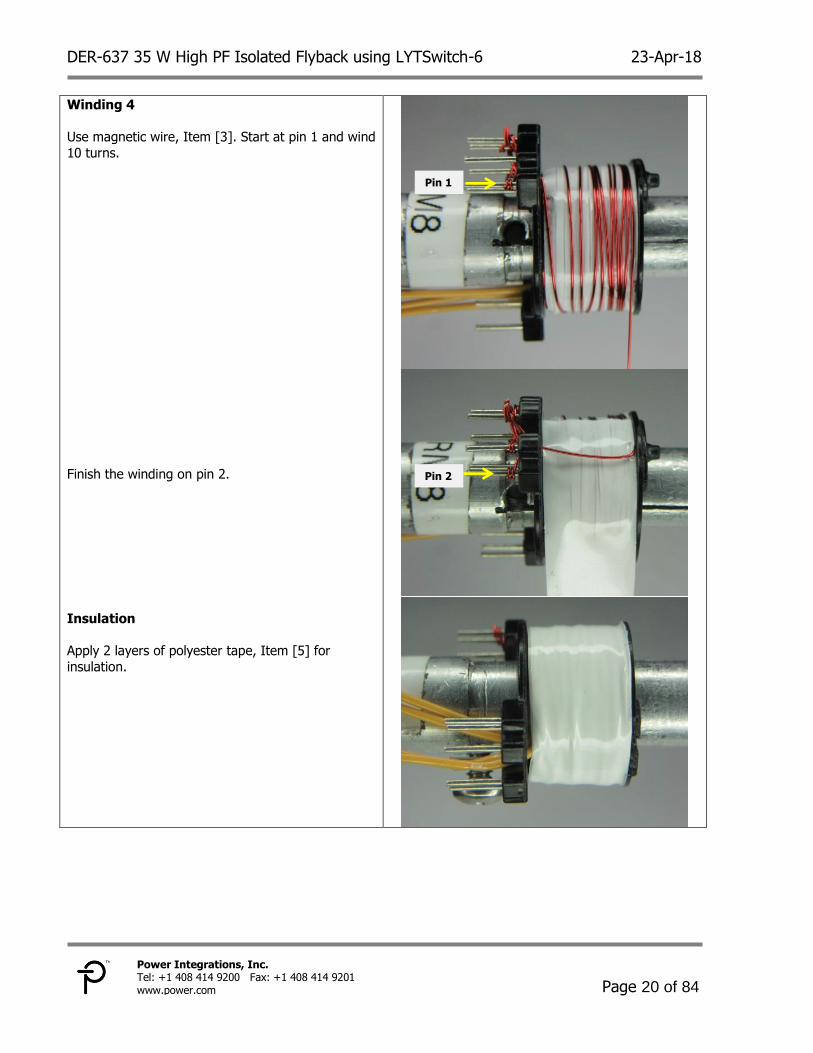
Winding 4 Use magnetic wire, Item [3]. Start at pin 1 and wind 10 turns. Finish the winding
on pin 2.
Insulation Apply 2 layers of polyester tape, Item [5] for insulation.
Core Grinding Grind the center leg of the ferrite core to meet the nominal inductance
specification of 720 H.
Assemble Core
Use RM8 core clips with terminals, Item [6] to fix the 2 cores into the bobbin.
Cut the terminal of the clip on the left side of the bobbin, looking at the bottom side facing the fly leads of the secondary winding.
Pins Cut any excess pins of the bobbin (pins without wire terminations). Trim pin 11 as short as possible.
Finish Dip the transformer in a 2:1 varnish and thinner solution
23-Apr-18 DER-637 35 W High PF Isolated Flyback using LYTSwitch-6
Page 17 of 84
Power Integrations Tel: +1 408 414 9200 Fax: +1 408 414 9201
www.power.com
Transformer Winding Illustrations 7.6
Winding Directions
Bobbin is oriented on winder jig such that terminal
pin 10-12 is in the right side. The winding direction is clockwise.
Winding 1
Use bifilar magnetic wire, Item [3]. Start at pin 10
and wind 30 turns evenly in 2 layers.
Finish the winding on pin 11.
Insulation
Apply 1 layer of polyester tape, Item [5] for insulation.
Pin 10
Pin 4
Pin 12
Pin 10
Pin 11
1 layer tape
DER-637 35 W High PF Isolated Flyback using LYTSwitch-6 23-Apr-18
Page 18 of 84
Power Integrations, Inc. Tel: +1 408 414 9200 Fax: +1 408 414 9201 www.power.com
Winding 2
Use bifilar triple insulated wire, Item [4]. Start at
the other side of the bobbin (pin 4 – pin 9 side) and
wind 9 turns evenly in 2 layers.
Finished the winding on the same side of the bobbin. Do not terminate the winding on any pin of
the bobbin; Just leave them as fly-leads.
Insulation
Apply 1 layer of polyester tape, Item [5] for
insulation.
Pin 10
23-Apr-18 DER-637 35 W High PF Isolated Flyback using LYTSwitch-6
Page 19 of 84
Power Integrations Tel: +1 408 414 9200 Fax: +1 408 414 9201
www.power.com
Winding 3
Use bifilar magnetic wire, Item [3]. Start at pin 11
and wind 29 turns evenly in 2 layers.
Finished the winding on pin 12.
Insulation
Apply 1 layer of polyester tape, Item [5] for
insulation.
Pin 12
Pin 11
Pin 12
DER-637 35 W High PF Isolated Flyback using LYTSwitch-6 23-Apr-18
Page 20 of 84
Power Integrations, Inc. Tel: +1 408 414 9200 Fax: +1 408 414 9201 www.power.com
Winding 4
Use magnetic wire, Item [3]. Start at pin 1 and wind
10 turns.
Finish the winding on pin 2.
Insulation
Apply 2 layers of polyester tape, Item [5] for
insulation.
Pin 1
Pin 2
23-Apr-18 DER-637 35 W High PF Isolated Flyback using LYTSwitch-6
Page 21 of 84
Power Integrations Tel: +1 408 414 9200 Fax: +1 408 414 9201
www.power.com
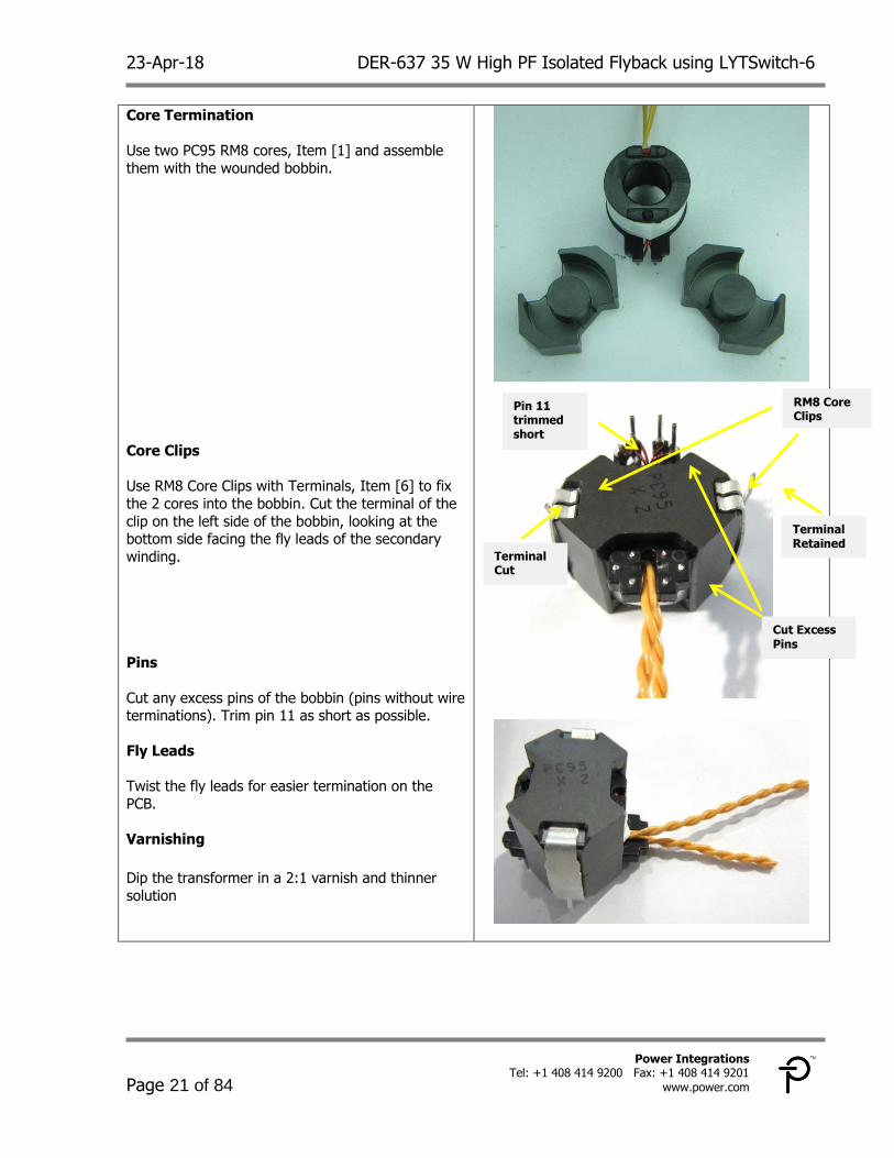
Core Termination
Use two PC95 RM8 cores, Item [1] and assemble
them with the wounded bobbin.
Core Clips
Use RM8 Core Clips with Terminals, Item [6] to fix
the 2 cores into the bobbin. Cut the terminal of the
clip on the left side of the bobbin, looking at the bottom side facing the fly leads of the secondary
winding.
Pins
Cut any excess pins of the bobbin (pins without wire terminations). Trim pin 11 as short as possible.
Fly Leads
Twist the fly leads for easier termination on the
PCB.
Varnishing
Dip the transformer in a 2:1 varnish and thinner
solution
Terminal Retained
RM8 Core Clips
Terminal Cut
Cut Excess
Pins
Pin 11 trimmed short
DER-637 35 W High PF Isolated Flyback using LYTSwitch-6 23-Apr-18
Page 22 of 84
Power Integrations, Inc. Tel: +1 408 414 9200 Fax: +1 408 414 9201 www.power.com
PFC Inductor (T2) Specifications 8
Electrical Diagram 8.1
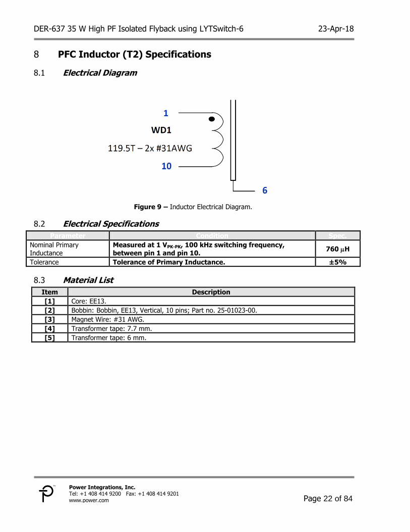
Figure 9 – Inductor Electrical Diagram.
Electrical Specifications 8.2
Parameter Condition Spec.
Nominal Primary
Inductance
Measured at 1 VPK-PK, 100 kHz switching frequency,
between pin 1 and pin 10. 760 H
Tolerance Tolerance of Primary Inductance. ±5%
Material List 8.3
Item Description
[1] Core: EE13.
[2] Bobbin: Bobbin, EE13, Vertical, 10 pins; Part no. 25-01023-00.
[3] Magnet Wire: #31 AWG.
[4] Transformer tape: 7.7 mm.
[5] Transformer tape: 6 mm.
23-Apr-18 DER-637 35 W High PF Isolated Flyback using LYTSwitch-6
Page 23 of 84
Power Integrations Tel: +1 408 414 9200 Fax: +1 408 414 9201
www.power.com
Inductor Build Diagram 8.4
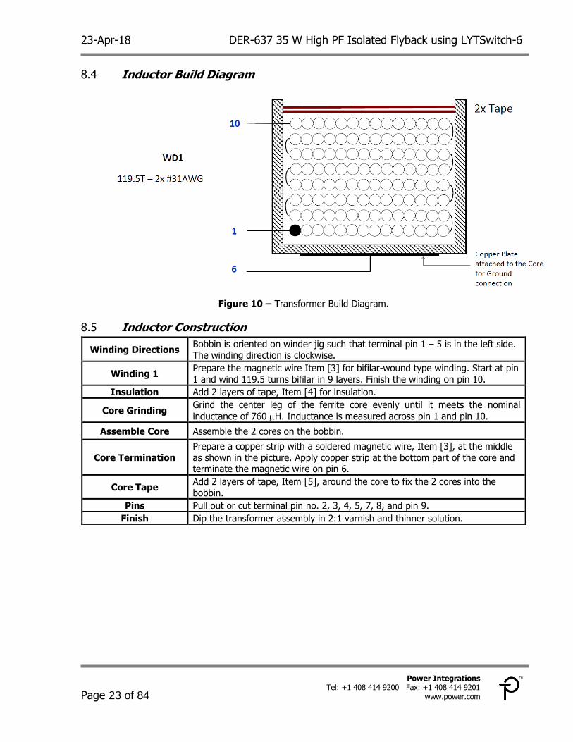
Figure 10 – Transformer Build Diagram.
Inductor Construction 8.5
Winding Directions Bobbin is oriented on winder jig such that terminal pin 1 – 5 is in the left side. The winding direction is clockwise.
Winding 1 Prepare the magnetic wire Item [3] for bifilar-wound type winding. Start at pin
1 and wind 119.5 turns bifilar in 9 layers. Finish the winding on pin 10.
Insulation Add 2 layers of tape, Item [4] for insulation.
Core Grinding Grind the center leg of the ferrite core evenly until it meets the nominal
inductance of 760 H. Inductance is measured across pin 1 and pin 10.
Assemble Core Assemble the 2 cores on the bobbin.
Core Termination
Prepare a copper strip with a soldered magnetic wire, Item [3], at the middle
as shown in the picture. Apply copper strip at the bottom part of the core and terminate the magnetic wire on pin 6.
Core Tape Add 2 layers of tape, Item [5], around the core to fix the 2 cores into the
bobbin.
Pins Pull out or cut terminal pin no. 2, 3, 4, 5, 7, 8, and pin 9.
Finish Dip the transformer assembly in 2:1 varnish and thinner solution.
DER-637 35 W High PF Isolated Flyback using LYTSwitch-6 23-Apr-18
Page 24 of 84
Power Integrations, Inc. Tel: +1 408 414 9200 Fax: +1 408 414 9201 www.power.com
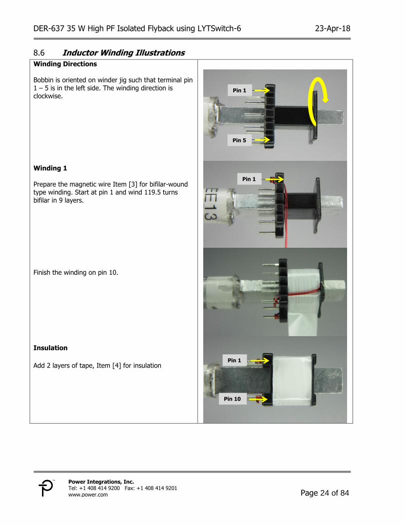
Inductor Winding Illustrations 8.6
Winding Directions
Bobbin is oriented on winder jig such that terminal pin
1 – 5 is in the left side. The winding direction is clockwise.
Winding 1
Prepare the magnetic wire Item [3] for bifilar-wound type winding. Start at pin 1 and wind 119.5 turns
bifilar in 9 layers.
Finish the winding on pin 10.
Insulation
Add 2 layers of tape, Item [4] for insulation
Pin 1
Pin 5
Pin 1
Pin 1
Pin 10
23-Apr-18 DER-637 35 W High PF Isolated Flyback using LYTSwitch-6
Page 25 of 84
Power Integrations Tel: +1 408 414 9200 Fax: +1 408 414 9201
www.power.com
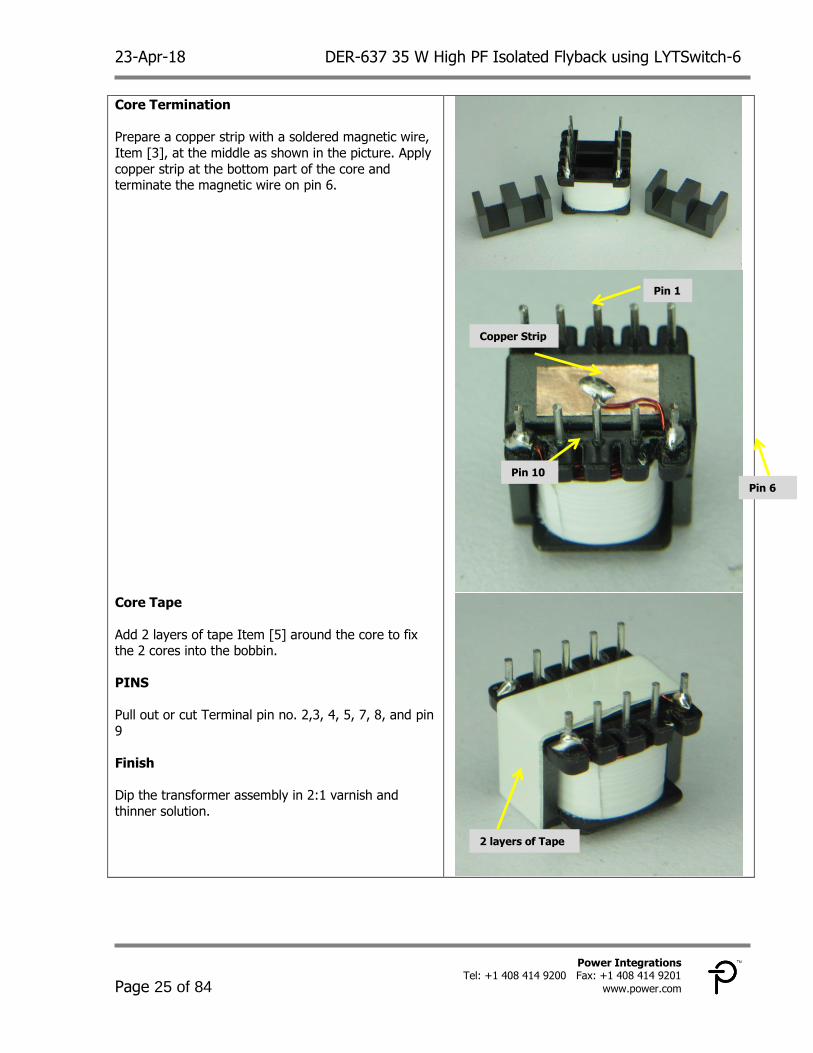
Core Termination
Prepare a copper strip with a soldered magnetic wire,
Item [3], at the middle as shown in the picture. Apply
copper strip at the bottom part of the core and terminate the magnetic wire on pin 6.
Core Tape
Add 2 layers of tape Item [5] around the core to fix the 2 cores into the bobbin.
PINS
Pull out or cut Terminal pin no. 2,3, 4, 5, 7, 8, and pin
9
Finish
Dip the transformer assembly in 2:1 varnish and
thinner solution.
Copper Strip
Pin 10
2 layers of Tape
Pin 6
Pin 1
DER-637 35 W High PF Isolated Flyback using LYTSwitch-6 23-Apr-18
Page 26 of 84
Power Integrations, Inc. Tel: +1 408 414 9200 Fax: +1 408 414 9201 www.power.com
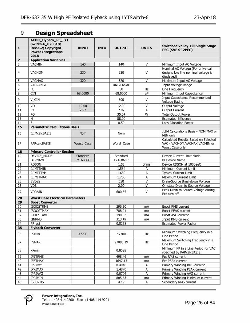
Design Spreadsheet 9
1
ACDC_Flyback_PF_LYTSwitch-6_020318; Rev.1.2; Copyright Power Integrations 2018
INPUT INFO OUTPUT UNITS Switched Valley-Fill Single Stage PFC (SVF S^2PFC)
2 Application Variables
3 VACMIN 140
140 V Minimum Input AC Voltage
4 VACNOM 230
230 V Nominal AC Voltage (For universal designs low line nominal voltage is displayed)
5 VACMAX 320
320 V Maximum Input AC Voltage
6 VACRANGE
UNIVERSAL
Input Voltage Range
7 FL
50 Hz Line Frequency
8 CIN 68.0000
68.0000 µF Minimum Input Capacitance
9 V_CIN
500 V Input Capacitance Recommended Voltage Rating
10 VO 12.00
12.00 V Output Voltage
11 IO 2.92
2.92 A Output Current
12 PO
35.04 W Total Output Power
13 N
88.00
Estimated Efficiency
14 Z
0.50
Loss Allocation Factor
15 Parametric Calculations Basis
16 ILIMcalcBASIS Nom
Nom
ILIM Calculations Basis - NOM,MAX or MIN only
17 PARcalcBASIS Worst_Case
Worst_Case
Calculated Results Based on Selected VAC - VACNOM,VACMAX,VACMIN or Worst Case only
18 Primary Controller Section
19 DEVICE_MODE Standard
Standard
Device Current Limit Mode
20 DEVNAME LYT6068C
LYT6068C
PI Device Name
21 RDSON
1.53 ohms Device RDSON at 100degC
22 ILIMITMIN
1.534 A Minimum Current Limit
23 ILIMITTYP
1.650 A Typical Current Limit
24 ILIMITMAX
1.766 A Maximum Current Limit
25 BVDSS
650 V Drain-Source Breakdown Voltage
26 VDS
2.00 V On state Drain to Source Voltage
27 VDRAIN
600.55 V Peak Drain to Source Voltage during Fet turn off
28 Worst Case Electrical Parameters
29 Boost Converter
30 IBOOSTRMS
296.90 mA Boost RMS current
31 IBOOSTMAX
788.21 mA Boost PEAK current
32 IBOOSTAVG
190.53 mA Boost AVG current
33 IINRMS
313.49 mA Input RMS current
34 PF_est
0.8258
Estimated Power Factor
35 Flyback Converter
36 FSMIN 47700
47700 Hz Minimum Switching Frequency in a Line Period
37 FSMAX
97880.19 Hz Maximum Switching Frequency in a Line Period
38 KPmin
0.8528
Minimum KP in a Line Period for VAC specified by PARcalcBASIS
39 IFETRMS
498.46 mA Fet RMS current
40 IFETMAX
1647.13 mA Fet PEAK current
41 IPRIRMS
0.4040 A Primary Winding RMS current
42 IPRIMAX
1.4870 A Primary Winding PEAK current
43 IPRIAVG
0.0704 A Primary Winding AVG current
44 IPRIMIN
885.63 mA Primary Winding Minimum current
45 ISECRMS
4.19 A Secondary RMS current
23-Apr-18 DER-637 35 W High PF Isolated Flyback using LYTSwitch-6
Page 27 of 84
Power Integrations Tel: +1 408 414 9200 Fax: +1 408 414 9201
www.power.com
46 ISECMAX
10.11 A Secondary PEAK current
47 Boost Choke Construction Parameters
48 RATIO_LBST_LFB 1.0555
1.0555
Boost Inductance and Flyback Primary Inductance Ratio
49 LBOOSTMIN
720.89 µH Minimum Boost Inductance
50 LBOOSTNOM
758.83 µH Nominal Boost Inductance
51 LBOOSTMAX
796.77 µH Maximum Boost Inductance
52 LBOOSTTOL 5.00
5.00 % Boost Inductance Tolerance
53 Boost Core and Bobbin Selection
54 CR_TYPE_BOOST EE13
EE13
Boost Core
55 CR_PN_BOOST
PC40EE13-Z
Boost Core Code
56 AE_BOOST
17.10 mm² Boost Core Cross Sectional Area
57 LE_BOOST
30.20 mm Boost Core Magnetic Path Length
58 AL_BOOST
1130.00 nH/turns² Boost Core Ungapped Core Effective Inductance
59 VE_BOOST
517.00 mm3 Boost Core Volume
60 BOBBINID_BOOST
548
Bobbin
61 AW_BOOST
22.20 mm² Window Area of Bobbin
62 BW_BOOST
7.40 mm Bobbin Width
63 MARGIN_BOOST
0.00 mm Safety Margin Width
64 BOBFILLFACTOR_Boost
40.32 % Boost Bobbin Fill Factor
65 Boost Winding Details
66 NBOOST 119.50
119.50
Boost Choke Turns
67 BP_BOOST
3057.81 Gauss Boost Peak Flux Density
68 ALG_BOOST
53.14 nH/turns² Boost Core Ungapped Core Effective Inductance
69 LG_BOOST
0.39 mm Boost Core Gap Length
70 L_BOOST 4.00
4.00
Number of Boost Layers
71 AWG_BOOST
31.00
Boost Winding Wire AWG
72 OD_BOOST_INSULATED
0.27 mm Boost Winding Wire Output Diameter with Insulation
73 OD_BOOST_BARE
0.23 mm Boost Winding Wire Output Diameter without Insulation
74 CMA_BOOST
269.68 Circular Mils/A Boost Winding Wire CMA
75 Flyback Transformer Construction Parameters
76 VOR 78
78 V Secondary Voltage Reflected in the Primary Winding
77 LP_MIN
682.98 µH Minimum Flyback Inductance
78 LP_NOM
718.93 µH Nominal Flyback Inductance
79 LP_MAX
754.88 µH Maximum Flyback Inductance
80 LP_TOL 5.00
5.00 % Flyback Inductance Tolerance
81 Flyback Core and Bobbin Selection
82 CR_TYPE RM8/I
RM8/I
Flyback Core
83 CR_PN
RM8/I-3F3
Flyback Core Code
84 AE
63.00 mm² Flyback Core Cross Sectional Area
85 LE
38.40 mm Flyback Core Magnetic Path Length
86 AL
3000.00 nH/turns² Flyback Core Ungapped Core Effective Inductance
87 VE
2440.00 mm3 Flyback Core Volume
88 BOBBINID
Ferroxcube
Flyback Bobbin
89 BB_ORIENTATION
H
Flyback Bobbin Orientation H -Horizontal and V -Vertical
90 AW
30.90 mm² Flyback Window Area of Bobbin
91 BW
8.60 mm Flyback Bobbin Width
92 MARGIN
0.00 mm Safety Margin Width
93 Flyback Winding Details
94 NP
59.00
Primary Turns
95 BP
3670.89 Gauss Flyback Peak Flux Density
96 BM
3533.33 Gauss Flyback Maximum Flux Density
97 BAC
1487.83 Gauss Flyback AC Flux Density
98 ALG
206.53 nH/turns² Flyback Core Ungapped Core Effective
DER-637 35 W High PF Isolated Flyback using LYTSwitch-6 23-Apr-18
Page 28 of 84
Power Integrations, Inc. Tel: +1 408 414 9200 Fax: +1 408 414 9201 www.power.com
Inductance
99 LG
0.36 mm Flyback Core Gap Length
100 L
2.00
Number of Flyback Layers
101 AWG
30.00
Primary Winding Wire AWG
102 OD
0.30 mm Primary Winding Wire Output Diameter with Insulation
103 DIA
0.26 mm Primary Winding Wire Output Diameter without Insulation
104 CMA
249.81 Circular Mils/A Primary Winding Wire CMA
105 NB
10.00
Bias Turns
106 L_BIAS
1.00
Number of Flyback Bias Winding Layers
107 AWGpBias
36.00
Bias Wire AWG
108 NS 9
9
Secondary Turns
109 AWGS
20.00
Secondary Winding Wire AWG
110 ODS
0.81 mm Secondary Winding Wire Output Diameter with Insulation
111 DIAS
1.12 mm Secondary Winding Wire Output Diameter without Insulation
112 CMAS
244.62 Circular Mils/A Secondary Winding Wire CMA
113 Primary Components Selection
114 Line Undervoltage
115 BROWN_IN_REQUIRED 85.00
85.00 V Required AC RMS line voltage brown-in threshold
116 RLS
2.10 MOhm Two Resistors of this Value in Series to the V-pin
117 BROWN_IN_ACTUAL
84.15 V Actual AC RMS brown-in threshold
118 Line Overvoltage
119 OVERVOLTAGE_LINE
350.90 V Actual AC RMS line over-voltage threshold
120 Bias Voltage
121 VBIAS 13.0
13.0 V Rectified Bias Voltage
122 VF_BIASDIODE
0.70 V Bias Winding Diode Forward Drop
123 VRRM_BIASDIODE
89.70 V Bias diode reverse voltage
124 CBIAS
22.0 µF Bias winding rectification capacitor
125 CBPP
0.47 µF BPP pin capacitor
126 Bulk Capacitor Zener Clamp
127 Use_Clamp
Yes
Bulk Capacitor Clamp Needed? Yes, No or N/A
128 VZ1_V
240.00 V Zener 1 Voltage Rating (In Series with Zener 2)
129 PZ1_W
1.25 W Zener 1 Minimum Power Rating
130 VZ2_V
240.00 V Zener 2 Voltage Rating
131 PZ2_W
1.25 W Zener 2 Minimum Power Rating
132 RZ
1000.00 ohms Resistor in series with Zener 1 and Zener 2
133 Secondary Components Selection
134 Feedback Components
135 RFB_UPPER
102.00 kOhm Upper feedback 1% resistor
136 RFB_LOWER
12.10 kOhm Lower feedback 1% resistor
137 CFB_LOWER
330.0 pF Lower feedback resistor decoupling at least 5V-rating capacitor
138 CBPS
2.2 µF BPS pin capacitor
139 Secondary Auxiliary Section - For VO > 24V ONLY
140 Sec Aux Diode
141 VAUX
12.00 V Rectified auxiliary voltage
142 VF_AUX
0.70 V Auxiliary winding diode forward drop
143 VRRM_AUXDIODE
82.03 V Auxiliary diode reverse voltage
144 CAUX
22.00 µF Auxiliary winding rectification capacitor
145 NAUX_SEC
9.00
Secondary Aux Turns
23-Apr-18 DER-637 35 W High PF Isolated Flyback using LYTSwitch-6
Page 29 of 84
Power Integrations Tel: +1 408 414 9200 Fax: +1 408 414 9201
www.power.com
146 L_AUX
1.00
Number of Flyback Aux Winding Layers
147 AWGSAUX
38
Secondary Aux Winding AWG
148 Output Parameters
149 VOUT_ACTUAL
12.00 V Actual Output Voltage
150 IOUT_ACTUAL
2.92 A Actual Output Current
151 ISECRMS
4.19 A Secondary RMS current for output
152 Output Components
153 VF
0.70 V Output diode forward drop
154 VRRM
81.03 V Output diode reverse voltage
155 COUT
2040.53 µF Output Capacitor - Capacitance
156 COUT_VOpercentRip
2.50 % Output Capacitor Ripple % of VOUT
157 ICOUTrms
3.00 A Output Capacitor Estimated Ripple Current
158 ESRmax
29.69 mohms Output Capacitor Maximum Recommended ESR
159 Errors, Warnings, Information
160 Information
VDRAIN,OVERVOLTAGE_L
INE
Although the design has passed the user should validate functionality on the bench. Please check the variables listed.
161 Design Warnings
Design variables whose values exceed electrical/datasheet specifications.
162 Design Errors
The list of design variables which result in an infeasible design.
Notes: Row 160 – Actual drain voltage stress does not exceed the absolute maximum VDS rating of LYTSwitch-6 IC. Actual line overvoltage protection is below the absolute maximum VDS rating of LYTSwitch-
6 IC.
DER-637 35 W High PF Isolated Flyback using LYTSwitch-6 23-Apr-18
Page 30 of 84
Power Integrations, Inc. Tel: +1 408 414 9200 Fax: +1 408 414 9201 www.power.com
Performance Data 10
All measurements were performed at room temperature.
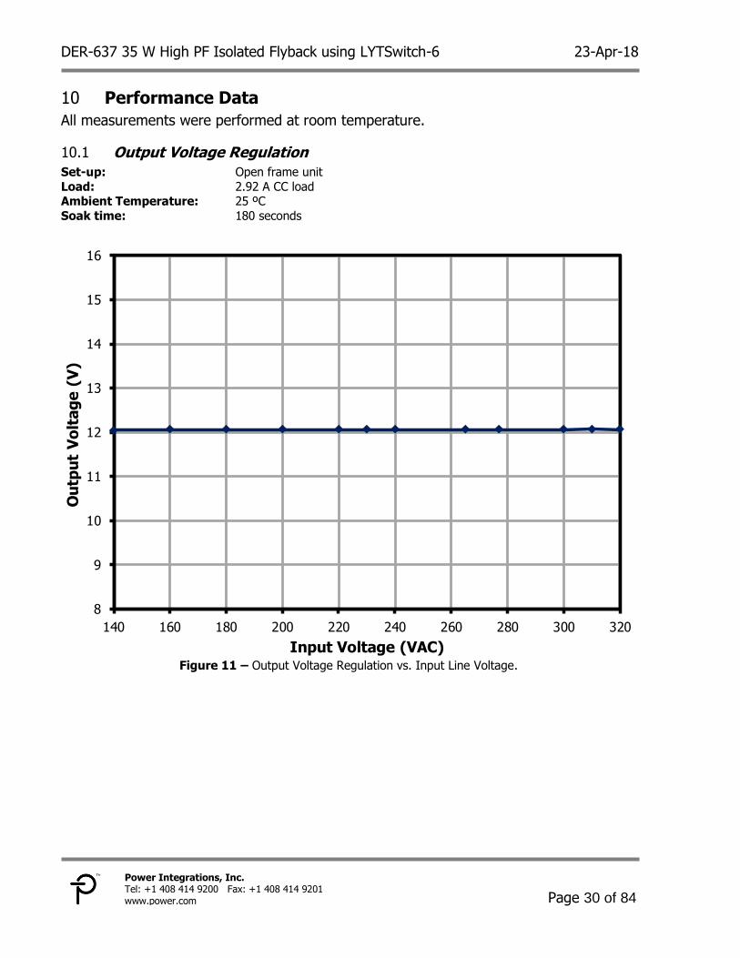
Output Voltage Regulation 10.1
Set-up: Open frame unit
Load: 2.92 A CC load Ambient Temperature: 25 ºC
Soak time: 180 seconds
Figure 11 – Output Voltage Regulation vs. Input Line Voltage.
8
9
10
11
12
13
14
15
16
140 160 180 200 220 240 260 280 300 320
Ou
tpu
t V
olt
ag
e (
V)
Input Voltage (VAC)
23-Apr-18 DER-637 35 W High PF Isolated Flyback using LYTSwitch-6
Page 31 of 84
Power Integrations Tel: +1 408 414 9200 Fax: +1 408 414 9201
www.power.com
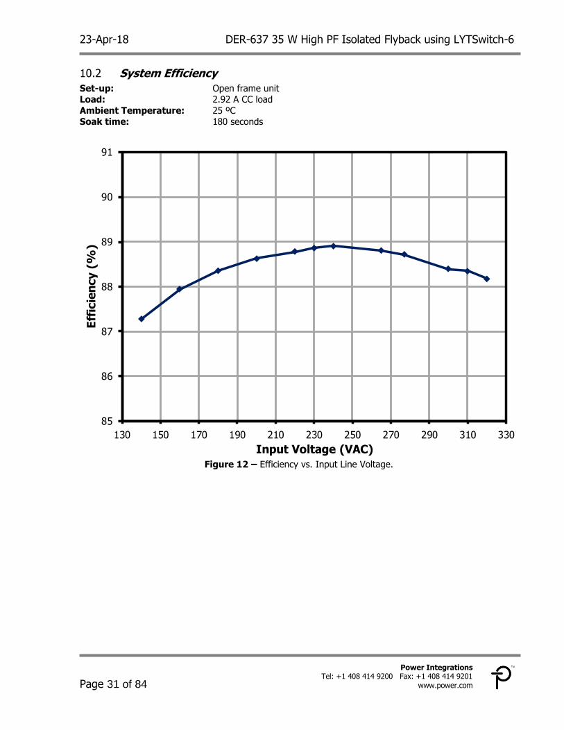
System Efficiency 10.2
Set-up: Open frame unit Load: 2.92 A CC load
Ambient Temperature: 25 ºC Soak time: 180 seconds
Figure 12 – Efficiency vs. Input Line Voltage.
85
86
87
88
89
90
91
130 150 170 190 210 230 250 270 290 310 330
Eff
icie
ncy (
%)
Input Voltage (VAC)
DER-637 35 W High PF Isolated Flyback using LYTSwitch-6 23-Apr-18
Page 32 of 84
Power Integrations, Inc. Tel: +1 408 414 9200 Fax: +1 408 414 9201 www.power.com
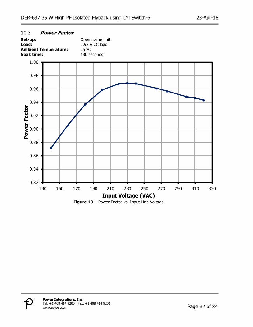
Power Factor 10.3
Set-up: Open frame unit Load: 2.92 A CC load
Ambient Temperature: 25 ºC Soak time: 180 seconds
Figure 13 – Power Factor vs. Input Line Voltage.
0.82
0.84
0.86
0.88
0.90
0.92
0.94
0.96
0.98
1.00
130 150 170 190 210 230 250 270 290 310 330
Po
wer
Facto
r
Input Voltage (VAC)
23-Apr-18 DER-637 35 W High PF Isolated Flyback using LYTSwitch-6
Page 33 of 84
Power Integrations Tel: +1 408 414 9200 Fax: +1 408 414 9201
www.power.com
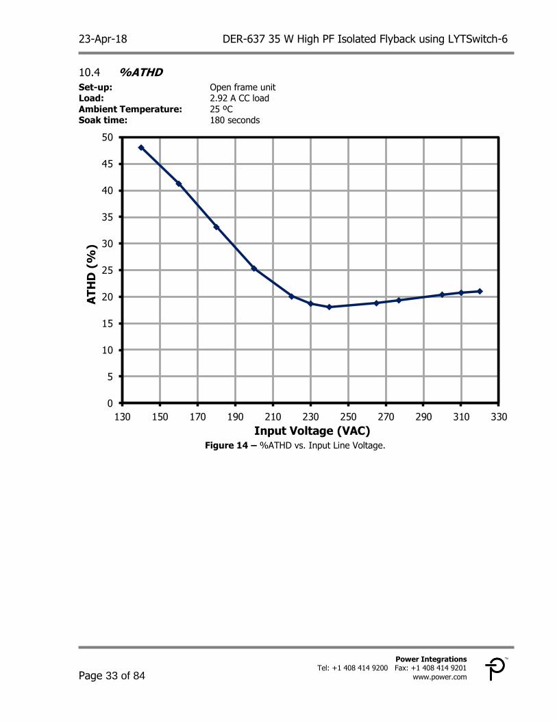
%ATHD 10.4
Set-up: Open frame unit Load: 2.92 A CC load
Ambient Temperature: 25 ºC Soak time: 180 seconds
Figure 14 – %ATHD vs. Input Line Voltage.
0
5
10
15
20
25
30
35
40
45
50
130 150 170 190 210 230 250 270 290 310 330
AT
HD
(%
)
Input Voltage (VAC)
DER-637 35 W High PF Isolated Flyback using LYTSwitch-6 23-Apr-18
Page 34 of 84
Power Integrations, Inc. Tel: +1 408 414 9200 Fax: +1 408 414 9201 www.power.com
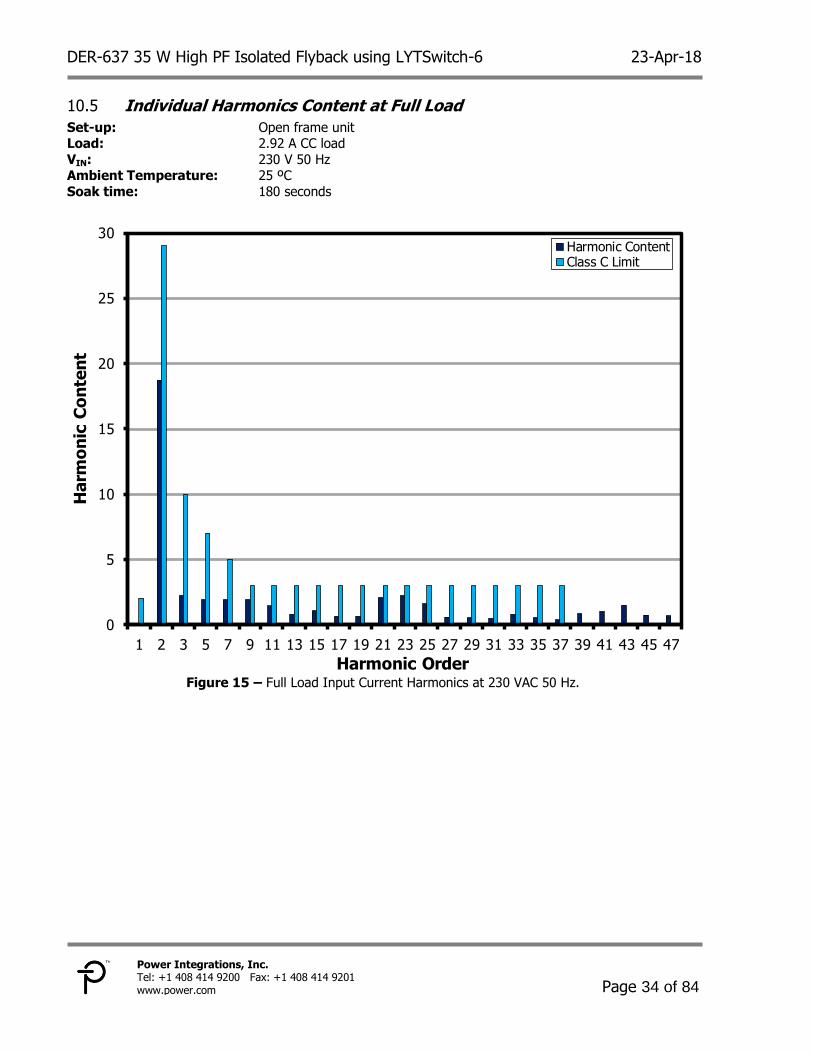
Individual Harmonics Content at Full Load 10.5
Set-up: Open frame unit Load: 2.92 A CC load
VIN: 230 V 50 Hz Ambient Temperature: 25 ºC
Soak time: 180 seconds
Figure 15 – Full Load Input Current Harmonics at 230 VAC 50 Hz.
0
5
10
15
20
25
30
1 2 3 5 7 9 11 13 15 17 19 21 23 25 27 29 31 33 35 37 39 41 43 45 47
Harm
on
ic C
on
ten
t
Harmonic Order
Harmonic ContentClass C Limit
23-Apr-18 DER-637 35 W High PF Isolated Flyback using LYTSwitch-6
Page 35 of 84
Power Integrations Tel: +1 408 414 9200 Fax: +1 408 414 9201
www.power.com
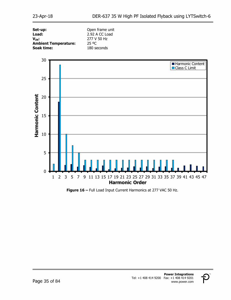
Set-up: Open frame unit
Load: 2.92 A CC Load VIN: 277 V 50 Hz
Ambient Temperature: 25 ºC Soak time: 180 seconds
Figure 16 – Full Load Input Current Harmonics at 277 VAC 50 Hz.
0
5
10
15
20
25
30
1 2 3 5 7 9 11 13 15 17 19 21 23 25 27 29 31 33 35 37 39 41 43 45 47
Harm
on
ic C
on
ten
t
Harmonic Order
Harmonic ContentClass C Limit
DER-637 35 W High PF Isolated Flyback using LYTSwitch-6 23-Apr-18
Page 36 of 84
Power Integrations, Inc. Tel: +1 408 414 9200 Fax: +1 408 414 9201 www.power.com
No-Load Input Power 10.6
Set-up: Open frame unit Load: Open load
Ambient Temperature: 25 ºC Soak time: 180 seconds
Figure 17 – No-Load Input Power vs. Input Line Voltage.
0
20
40
60
80
100
120
140
130 150 170 190 210 230 250 270 290 310 330
No
-Lo
ad
In
pu
t P
ow
er
(mW
)
Input Voltage (VAC)
23-Apr-18 DER-637 35 W High PF Isolated Flyback using LYTSwitch-6
Page 37 of 84
Power Integrations Tel: +1 408 414 9200 Fax: +1 408 414 9201
www.power.com
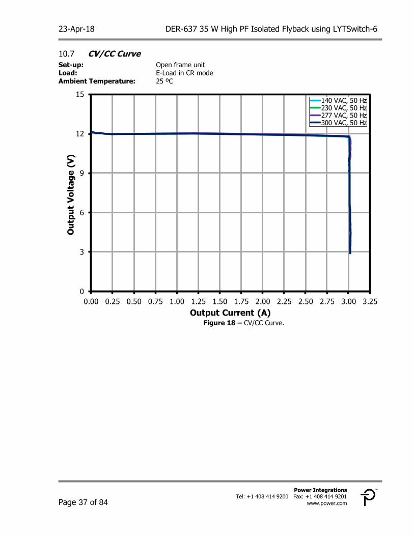
CV/CC Curve 10.7
Set-up: Open frame unit Load: E-Load in CR mode
Ambient Temperature: 25 ºC
Figure 18 – CV/CC Curve.
0
3
6
9
12
15
0.00 0.25 0.50 0.75 1.00 1.25 1.50 1.75 2.00 2.25 2.50 2.75 3.00 3.25
Ou
tpu
t V
olt
ag
e (
V)
Output Current (A)
140 VAC, 50 Hz230 VAC, 50 Hz277 VAC, 50 Hz300 VAC, 50 Hz
DER-637 35 W High PF Isolated Flyback using LYTSwitch-6 23-Apr-18
Page 38 of 84
Power Integrations, Inc. Tel: +1 408 414 9200 Fax: +1 408 414 9201 www.power.com
Test Data 11
Test Data at Full Load 11.1
Input Input Measurement LED Load Measurement Efficiency
(%) VAC
(VRMS) Freq (Hz)
VIN (VRMS)
IIN (mARMS)
PIN (W)
PF %ATHD VOUT (VDC)
IOUT (mADC)
POUT (W)
140 50 139.96 330.37 40.31 0.872 48.04 12.05 2919.80 35.18 87.27
160 50 159.92 276.59 40.06 0.906 41.28 12.07 2919.80 35.23 87.95
180 50 179.97 236.51 39.88 0.937 33.09 12.07 2919.80 35.23 88.35
200 50 199.92 207.49 39.76 0.959 25.31 12.07 2919.80 35.24 88.63
220 50 219.96 186.47 39.69 0.968 20.08 12.07 2919.80 35.24 88.78
230 50 229.99 177.99 39.65 0.969 18.74 12.07 2919.70 35.23 88.86
240 50 240.01 170.58 39.63 0.968 18.05 12.07 2919.70 35.23 88.90
265 50 265.03 155.84 39.68 0.961 18.83 12.07 2919.70 35.24 88.80
277 50 277.02 149.89 39.72 0.957 19.35 12.07 2919.80 35.24 88.72
300 50 300.07 140.13 39.86 0.948 20.42 12.07 2919.70 35.23 88.39
310 50 309.84 136.14 39.92 0.947 20.79 12.08 2919.80 35.27 88.35
320 50 319.75 132.56 39.97 0.943 21.04 12.07 2919.70 35.24 88.17
Test Data at No-Load 11.2
Input Input Measurement Output Measurement
VAC (VRMS)
Freq (Hz)
VIN (VRMS)
IIN (mARMS)
PIN (W)
PF %ATHD VOUT (VDC)
140 50 140.03 10.29 0.037 0.026 48.28 12.19
160 50 159.98 10.51 0.052 0.031 14.79 12.19
180 50 180.02 10.82 0.062 0.032 34.03 12.19
200 50 199.97 11.30 0.069 0.030 28.46 12.19
220 50 220.00 12.03 0.076 0.029 11.69 12.19
230 50 230.02 12.46 0.074 0.026 21.99 12.19
240 50 240.04 12.92 0.075 0.024 20.81 12.19
265 50 265.07 14.01 0.091 0.024 20.94 12.19
277 50 277.06 14.45 0.091 0.023 8.78 12.19
300 50 300.10 15.13 0.105 0.023 20.94 12.19
310 50 310.32 12.57 0.107 0.028 5.44 12.19
320 50 320.22 12.98 0.119 0.029 6.13 12.19
23-Apr-18 DER-637 35 W High PF Isolated Flyback using LYTSwitch-6
Page 39 of 84
Power Integrations Tel: +1 408 414 9200 Fax: +1 408 414 9201
www.power.com
Individual Harmonic Content at 230 VAC 50 Hz and Full Load 11.3
V Freq IIN
(mARMS) P PF %THD
230 50.00 179.08 39.870 0.968 19.466
nth
Order mA
Content %
Content mA Limit <25 W
% Limit >25 W
Remarks
1 175.32
2 0.09 0.05%
2.00% Pass
3 32.83 18.73% 135.56 29.04% Pass
5 3.91 2.23% 75.75 10.00% Pass
7 3.35 1.91% 39.87 7.00% Pass
9 3.33 1.90% 19.94 5.00% Pass
11 3.34 1.91% 13.95 3.00% Pass
13 2.52 1.44% 11.81 3.00% Pass
15 1.41 0.80% 10.23 3.00% Pass
17 1.81 1.03% 9.03 3.00% Pass
19 1.10 0.63% 8.08 3.00% Pass
21 1.11 0.63% 7.31 3.00% Pass
23 3.66 2.09% 6.67 3.00% Pass
25 3.86 2.20% 6.14 3.00% Pass
27 2.77 1.58% 5.69 3.00% Pass
29 1.05 0.60% 5.29 3.00% Pass
31 0.93 0.53% 4.95 3.00% Pass
33 0.81 0.46% 4.65 3.00% Pass
35 1.36 0.78% 4.39 3.00% Pass
37 0.93 0.53% 4.15 3.00% Pass
39 0.65 0.37% 3.94 3.00% Pass
41 1.47 0.84%
43 1.74 0.99%
45 2.56 1.46%
47 1.27 0.72%
49 1.15 0.66%
DER-637 35 W High PF Isolated Flyback using LYTSwitch-6 23-Apr-18
Page 40 of 84
Power Integrations, Inc. Tel: +1 408 414 9200 Fax: +1 408 414 9201 www.power.com
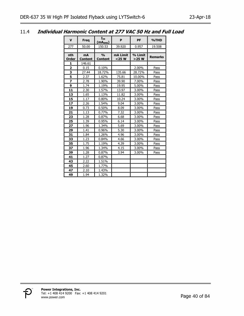
Individual Harmonic Content at 277 VAC 50 Hz and Full Load 11.4
V Freq IIN
(mARMS) P PF %THD
277 50.00 150.53 39.920 0.957 19.508
nth
Order mA
Content %
Content mA Limit <25 W
% Limit >25 W
Remarks
1 146.61
2 0.15 0.10%
2.00% Pass
3 27.44 18.72% 135.66 28.72% Pass
5 2.37 1.62% 75.81 10.00% Pass
7 2.78 1.90% 39.90 7.00% Pass
9 1.74 1.19% 19.95 5.00% Pass
11 2.30 1.57% 13.97 3.00% Pass
13 1.65 1.13% 11.82 3.00% Pass
15 1.17 0.80% 10.24 3.00% Pass
17 2.26 1.54% 9.04 3.00% Pass
19 0.73 0.50% 8.09 3.00% Pass
21 1.13 0.77% 7.32 3.00% Pass
23 1.28 0.87% 6.68 3.00% Pass
25 1.39 0.95% 6.14 3.00% Pass
27 1.96 1.34% 5.69 3.00% Pass
29 1.41 0.96% 5.30 3.00% Pass
31 1.84 1.26% 4.96 3.00% Pass
33 1.23 0.84% 4.66 3.00% Pass
35 1.75 1.19% 4.39 3.00% Pass
37 1.96 1.34% 4.15 3.00% Pass
39 1.28 0.87% 3.94 3.00% Pass
41 1.27 0.87%
43 2.22 1.51%
45 2.60 1.77%
47 2.10 1.43%
49 1.94 1.32%
23-Apr-18 DER-637 35 W High PF Isolated Flyback using LYTSwitch-6
Page 41 of 84
Power Integrations Tel: +1 408 414 9200 Fax: +1 408 414 9201
www.power.com
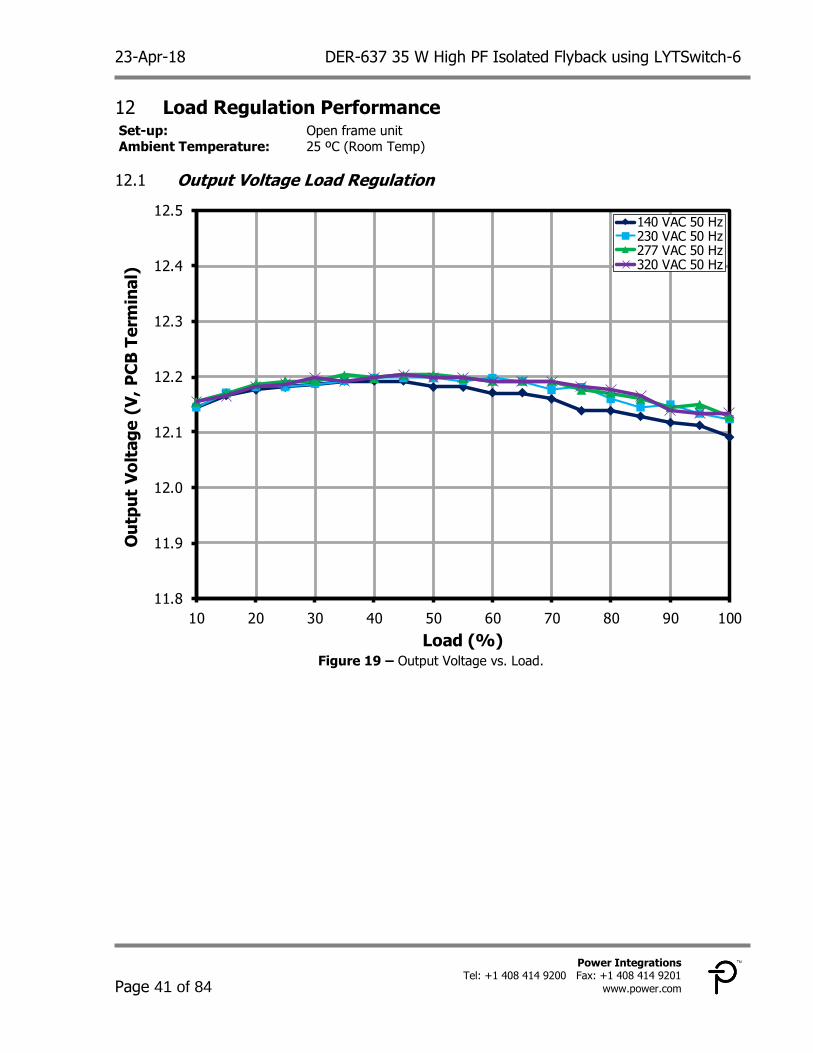
Load Regulation Performance 12Set-up: Open frame unit Ambient Temperature: 25 ºC (Room Temp)
Output Voltage Load Regulation 12.1
Figure 19 – Output Voltage vs. Load.
11.8
11.9
12.0
12.1
12.2
12.3
12.4
12.5
10 20 30 40 50 60 70 80 90 100
Ou
tpu
t V
olt
ag
e (
V,
PC
B T
erm
inal)
Load (%)
140 VAC 50 Hz230 VAC 50 Hz277 VAC 50 Hz320 VAC 50 Hz
DER-637 35 W High PF Isolated Flyback using LYTSwitch-6 23-Apr-18
Page 42 of 84
Power Integrations, Inc. Tel: +1 408 414 9200 Fax: +1 408 414 9201 www.power.com
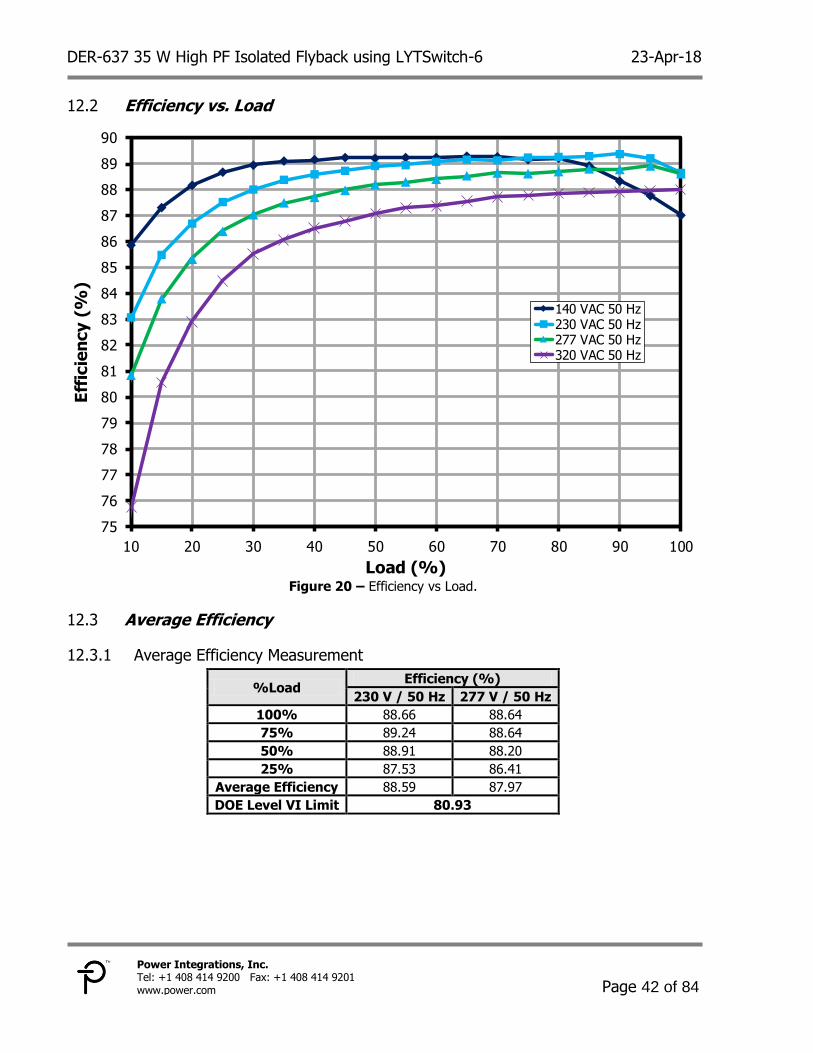
Efficiency vs. Load 12.2
Figure 20 – Efficiency vs Load.
Average Efficiency 12.3
Average Efficiency Measurement 12.3.1
%Load Efficiency (%)
230 V / 50 Hz 277 V / 50 Hz
100% 88.66 88.64
75% 89.24 88.64
50% 88.91 88.20
25% 87.53 86.41
Average Efficiency 88.59 87.97
DOE Level VI Limit 80.93
75
76
77
78
79
80
81
82
83
84
85
86
87
88
89
90
10 20 30 40 50 60 70 80 90 100
Eff
icie
ncy (
%)
Load (%)
140 VAC 50 Hz230 VAC 50 Hz277 VAC 50 Hz320 VAC 50 Hz
23-Apr-18 DER-637 35 W High PF Isolated Flyback using LYTSwitch-6
Page 43 of 84
Power Integrations Tel: +1 408 414 9200 Fax: +1 408 414 9201
www.power.com
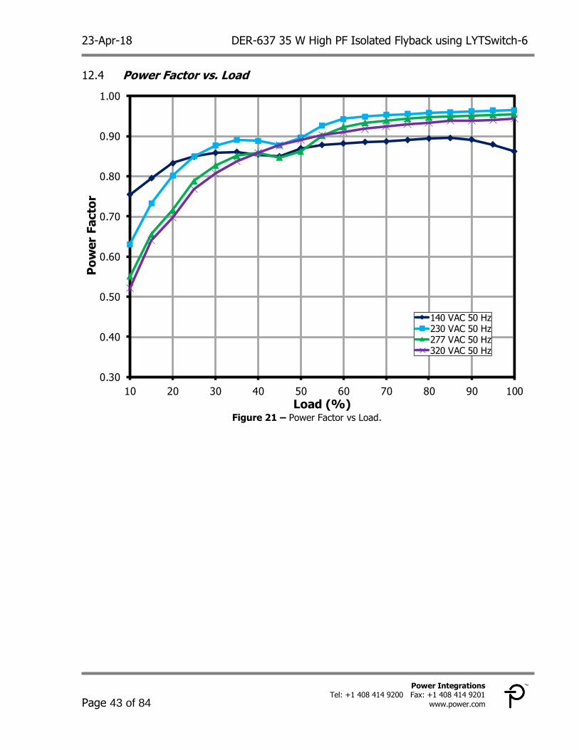
Power Factor vs. Load 12.4
Figure 21 – Power Factor vs Load.
0.30
0.40
0.50
0.60
0.70
0.80
0.90
1.00
10 20 30 40 50 60 70 80 90 100
Po
wer
Fa
cto
r
Load (%)
140 VAC 50 Hz230 VAC 50 Hz277 VAC 50 Hz320 VAC 50 Hz
DER-637 35 W High PF Isolated Flyback using LYTSwitch-6 23-Apr-18
Page 44 of 84
Power Integrations, Inc. Tel: +1 408 414 9200 Fax: +1 408 414 9201 www.power.com
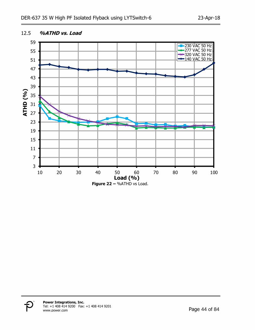
%ATHD vs. Load 12.5
Figure 22 – %ATHD vs Load.
3
7
11
15
19
23
27
31
35
39
43
47
51
55
59
10 20 30 40 50 60 70 80 90 100
AT
HD
(%
)
Load (%)
230 VAC 50 Hz277 VAC 50 Hz320 VAC 50 Hz140 VAC 50 Hz
23-Apr-18 DER-637 35 W High PF Isolated Flyback using LYTSwitch-6
Page 45 of 84
Power Integrations Tel: +1 408 414 9200 Fax: +1 408 414 9201
www.power.com
Thermal Performance 13
Thermal Measurements at Room Temp Ambient 13.1
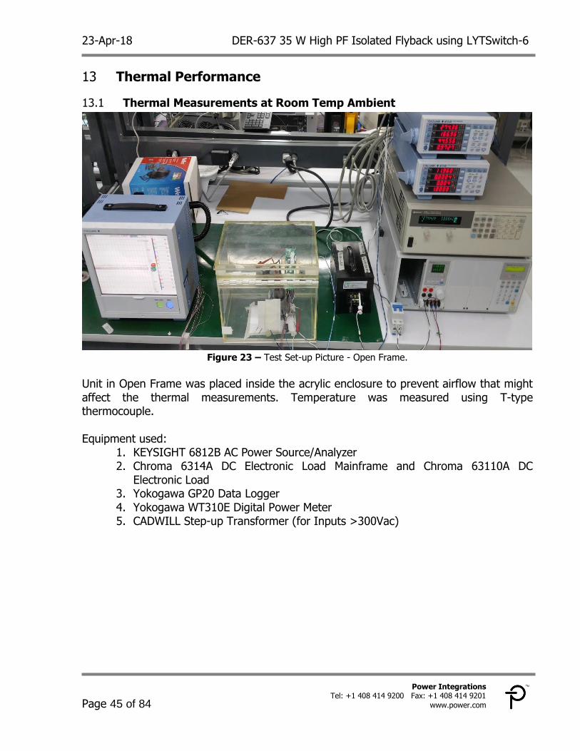
Figure 23 – Test Set-up Picture - Open Frame.
Unit in Open Frame was placed inside the acrylic enclosure to prevent airflow that might affect the thermal measurements. Temperature was measured using T-type thermocouple. Equipment used:
1. KEYSIGHT 6812B AC Power Source/Analyzer 2. Chroma 6314A DC Electronic Load Mainframe and Chroma 63110A DC
Electronic Load 3. Yokogawa GP20 Data Logger 4. Yokogawa WT310E Digital Power Meter 5. CADWILL Step-up Transformer (for Inputs >300Vac)
DER-637 35 W High PF Isolated Flyback using LYTSwitch-6 23-Apr-18
Page 46 of 84
Power Integrations, Inc. Tel: +1 408 414 9200 Fax: +1 408 414 9201 www.power.com
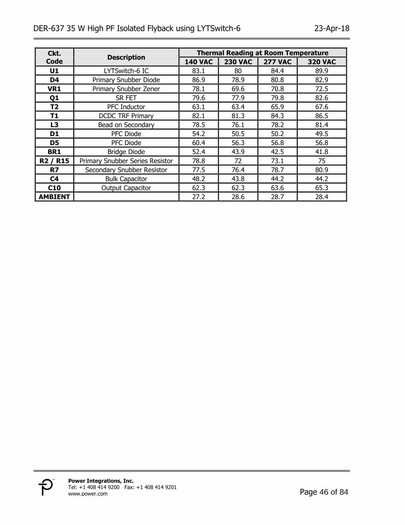
Ckt. Code
Description Thermal Reading at Room Temperature
140 VAC 230 VAC 277 VAC 320 VAC
U1 LYTSwitch-6 IC 83.1 80 84.4 89.9
D4 Primary Snubber Diode 86.9 78.9 80.8 82.9
VR1 Primary Snubber Zener 78.1 69.6 70.8 72.5
Q1 SR FET 79.6 77.9 79.8 82.6
T2 PFC Inductor 63.1 63.4 65.9 67.6
T1 DCDC TRF Primary 82.1 81.3 84.3 86.5
L3 Bead on Secondary 78.5 76.1 78.2 81.4
D1 PFC Diode 54.2 50.5 50.2 49.5
D5 PFC Diode 60.4 56.3 56.8 56.8
BR1 Bridge Diode 52.4 43.9 42.5 41.8
R2 / R15 Primary Snubber Series Resistor 78.8 72 73.1 75
R7 Secondary Snubber Resistor 77.5 76.4 78.7 80.9
C4 Bulk Capacitor 48.2 43.8 44.2 44.2
C10 Output Capacitor 62.3 62.3 63.6 65.3
AMBIENT
27.2 28.6 28.7 28.4
23-Apr-18 DER-637 35 W High PF Isolated Flyback using LYTSwitch-6
Page 47 of 84
Power Integrations Tel: +1 408 414 9200 Fax: +1 408 414 9201
www.power.com
Thermal Performance at High Temp Ambient 13.2
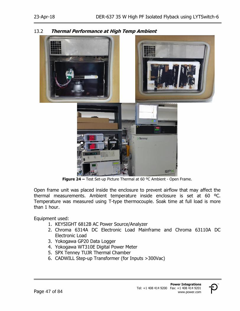
Figure 24 – Test Set-up Picture Thermal at 60 ºC Ambient - Open Frame.
Open frame unit was placed inside the enclosure to prevent airflow that may affect the thermal measurements. Ambient temperature inside enclosure is set at 60 ºC. Temperature was measured using T-type thermocouple. Soak time at full load is more than 1 hour. Equipment used:
1. KEYSIGHT 6812B AC Power Source/Analyzer 2. Chroma 6314A DC Electronic Load Mainframe and Chroma 63110A DC
Electronic Load 3. Yokogawa GP20 Data Logger 4. Yokogawa WT310E Digital Power Meter 5. SPX Tenney TUJR Thermal Chamber 6. CADWILL Step-up Transformer (for Inputs >300Vac)
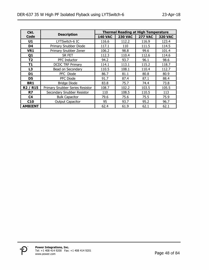
DER-637 35 W High PF Isolated Flyback using LYTSwitch-6 23-Apr-18
Page 48 of 84
Power Integrations, Inc. Tel: +1 408 414 9200 Fax: +1 408 414 9201 www.power.com
Ckt.
Code Description
Thermal Reading at High Temperature
140 VAC 230 VAC 277 VAC 320 VAC
U1 LYTSwitch-6 IC 116.6 112.2 116.9 123.4
D4 Primary Snubber Diode 117.1 110 111.5 114.5
VR1 Primary Snubber Zener 106.2 98.8 99.6 101.4
Q1 SR FET 112.3 110.4 112.6 114.6
T2 PFC Inductor 94.2 93.7 96.1 98.6
T1 DCDC TRF Primary 114.1 113.1 115.2 118.7
L3 Bead on Secondary 110.5 108.1 110.4 112.7
D1 PFC Diode 86.7 81.1 80.8 80.9
D5 PFC Diode 91.7 87.4 87.1 88.4
BR1 Bridge Diode 83.8 75.7 74.4 73.8
R2 / R15 Primary Snubber Series Resistor 108.7 102.2 103.5 105.5
R7 Secondary Snubber Resistor 110 108.5 110.5 113
C4 Bulk Capacitor 79.6 75.6 75.5 75.9
C10 Output Capacitor 95 93.7 95.2 96.7
AMBIENT
62.4 61.9 62.1 62.1
23-Apr-18 DER-637 35 W High PF Isolated Flyback using LYTSwitch-6
Page 49 of 84
Power Integrations Tel: +1 408 414 9200 Fax: +1 408 414 9201
www.power.com
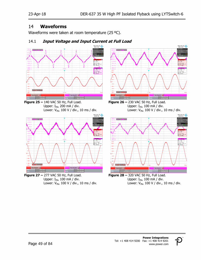
Waveforms 14
Waveforms were taken at room temperature (25 ºC).
Input Voltage and Input Current at Full Load 14.1
Figure 25 – 140 VAC 50 Hz, Full Load.
Upper: IIN, 200 mA / div.
Lower: VIN, 100 V / div., 10 ms / div.
Figure 26 – 230 VAC 50 Hz, Full Load. Upper: IIN, 100 mA / div.
Lower: VIN, 100 V / div., 10 ms / div.
Figure 27 – 277 VAC 50 Hz, Full Load.
Upper: IIN, 100 mA / div. Lower: VIN, 100 V / div., 10 ms / div.
Figure 28 – 320 VAC 50 Hz, Full Load.
Upper: IIN, 100 mA / div. Lower: VIN, 100 V / div., 10 ms / div.
DER-637 35 W High PF Isolated Flyback using LYTSwitch-6 23-Apr-18
Page 50 of 84
Power Integrations, Inc. Tel: +1 408 414 9200 Fax: +1 408 414 9201 www.power.com
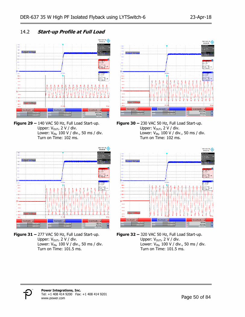
Start-up Profile at Full Load 14.2
Figure 29 – 140 VAC 50 Hz, Full Load Start-up.
Upper: VOUT, 2 V / div. Lower: VIN, 100 V / div., 50 ms / div.
Turn on Time: 102 ms.
Figure 30 – 230 VAC 50 Hz, Full Load Start-up.
Upper: VOUT, 2 V / div. Lower: VIN, 100 V / div., 50 ms / div.
Turn on Time: 102 ms.
Figure 31 – 277 VAC 50 Hz, Full Load Start-up. Upper: VOUT, 2 V / div.
Lower: VIN, 100 V / div., 50 ms / div. Turn on Time: 101.5 ms.
Figure 32 – 320 VAC 50 Hz, Full Load Start-up. Upper: VOUT, 2 V / div.
Lower: VIN, 100 V / div., 50 ms / div. Turn on Time: 101.5 ms.
23-Apr-18 DER-637 35 W High PF Isolated Flyback using LYTSwitch-6
Page 51 of 84
Power Integrations Tel: +1 408 414 9200 Fax: +1 408 414 9201
www.power.com
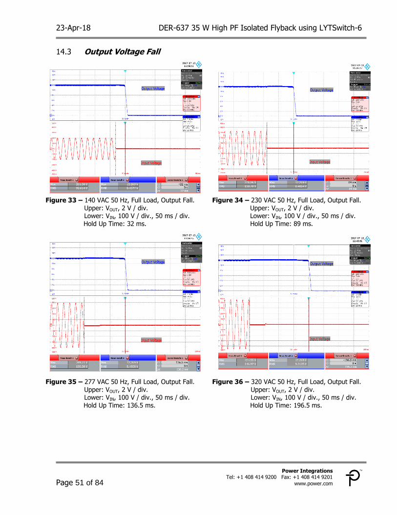
Output Voltage Fall 14.3
Figure 33 – 140 VAC 50 Hz, Full Load, Output Fall.
Upper: VOUT, 2 V / div. Lower: VIN, 100 V / div., 50 ms / div.
Hold Up Time: 32 ms.
Figure 34 – 230 VAC 50 Hz, Full Load, Output Fall.
Upper: VOUT, 2 V / div. Lower: VIN, 100 V / div., 50 ms / div.
Hold Up Time: 89 ms.
Figure 35 – 277 VAC 50 Hz, Full Load, Output Fall.
Upper: VOUT, 2 V / div. Lower: VIN, 100 V / div., 50 ms / div.
Hold Up Time: 136.5 ms.
Figure 36 – 320 VAC 50 Hz, Full Load, Output Fall.
Upper: VOUT, 2 V / div. Lower: VIN, 100 V / div., 50 ms / div.
Hold Up Time: 196.5 ms.
DER-637 35 W High PF Isolated Flyback using LYTSwitch-6 23-Apr-18
Page 52 of 84
Power Integrations, Inc. Tel: +1 408 414 9200 Fax: +1 408 414 9201 www.power.com
Power Cycling 14.4
Figure 37 – 230 VAC 50 Hz, Full Load.
1 s Off, 1 s On.
Upper: VOUT, 2 V / div. Lower: VIN, 100 V / div., 4 s / div.
Figure 38 – 277 VAC 50 Hz, Full Load.
1 s Off, 1 s On.
Upper: VOUT, 2 V / div. Lower: VIN, 100 V / div., 4 s / div.
Figure 39 – 230 VAC 50 Hz, Full Load. 0.3 s Off, 0.3 s On.
Upper: VOUT, 2 V / div. Lower: VIN, 100 V / div., 1 s / div.
Figure 40 – 277 VAC 50 Hz, Full Load. 0.3 s Off, 0.3 s On.
Upper: VOUT, 2 V / div. Lower: VIN, 100 V / div., 1 s / div.
23-Apr-18 DER-637 35 W High PF Isolated Flyback using LYTSwitch-6
Page 53 of 84
Power Integrations Tel: +1 408 414 9200 Fax: +1 408 414 9201
www.power.com
Load Transient Response 3 Hz 14.5
Figure 41 – 230 VAC 50 Hz.
0% to 100% Load Change. 3 Hz, 50% Duty Cycle.
Slew Rate: 800 mA / s.
Upper: VOUT, 2 V / div., 200 ms / div. Lower: IOUT, 1 A / div.
Figure 42 – 230 VAC 50 Hz.
25% to 100% Load Change. 3 Hz, 50% Duty Cycle.
Slew Rate: 800 mA / s.
Upper: VOUT, 2 V / div., 200 ms / div. Lower: IOUT, 1 A / div.
Figure 43 – 230 VAC 50 Hz.
50% to 100% Load Change. 3 Hz, 50% Duty Cycle.
Slew Rate: 800 mA / s.
Upper: VOUT, 2 V / div., 200 ms / div.
Lower: IOUT, 1 A / div.
Figure 44 – 230 VAC 50 Hz.
75% to 100% Load Change. 3 Hz, 50% Duty Cycle.
Slew Rate: 800 mA / s.
Upper: VOUT, 2 V / div., 200 ms / div.
Lower: IOUT, 1 A / div.
DER-637 35 W High PF Isolated Flyback using LYTSwitch-6 23-Apr-18
Page 54 of 84
Power Integrations, Inc. Tel: +1 408 414 9200 Fax: +1 408 414 9201 www.power.com
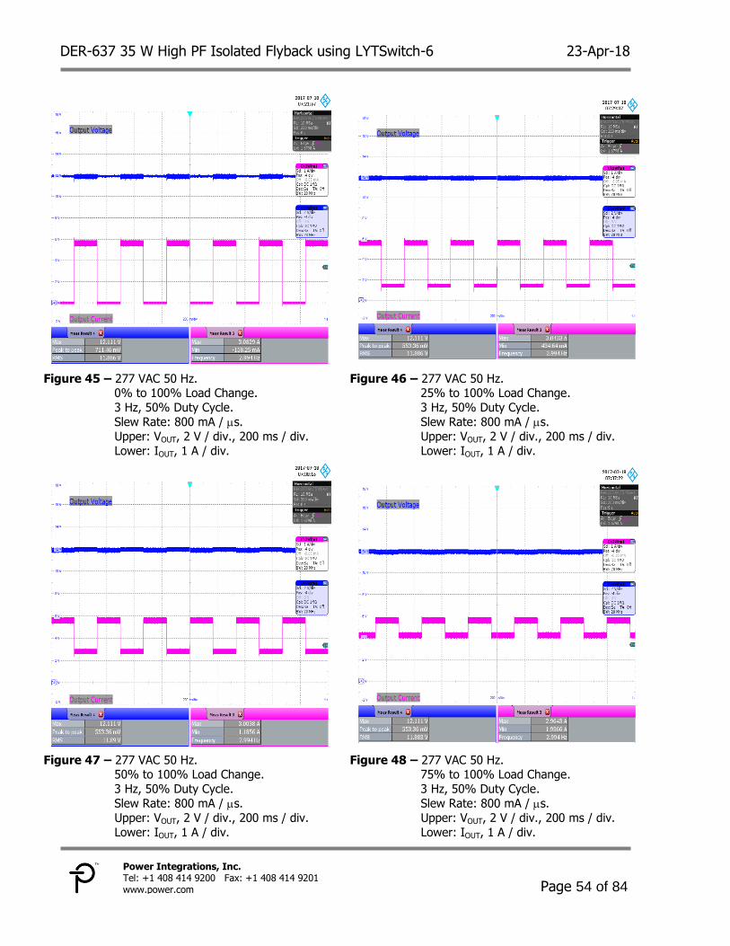
Figure 45 – 277 VAC 50 Hz. 0% to 100% Load Change.
3 Hz, 50% Duty Cycle.
Slew Rate: 800 mA / s.
Upper: VOUT, 2 V / div., 200 ms / div.
Lower: IOUT, 1 A / div.
Figure 46 – 277 VAC 50 Hz. 25% to 100% Load Change.
3 Hz, 50% Duty Cycle.
Slew Rate: 800 mA / s.
Upper: VOUT, 2 V / div., 200 ms / div.
Lower: IOUT, 1 A / div.
Figure 47 – 277 VAC 50 Hz. 50% to 100% Load Change.
3 Hz, 50% Duty Cycle.
Slew Rate: 800 mA / s.
Upper: VOUT, 2 V / div., 200 ms / div.
Lower: IOUT, 1 A / div.
Figure 48 – 277 VAC 50 Hz. 75% to 100% Load Change.
3 Hz, 50% Duty Cycle.
Slew Rate: 800 mA / s.
Upper: VOUT, 2 V / div., 200 ms / div.
Lower: IOUT, 1 A / div.
23-Apr-18 DER-637 35 W High PF Isolated Flyback using LYTSwitch-6
Page 55 of 84
Power Integrations Tel: +1 408 414 9200 Fax: +1 408 414 9201
www.power.com
Load Transient Response 100 Hz 14.6
Figure 49 – 230 VAC 50 Hz.
0% to 100% Load Change.
100 Hz, 50% Duty Cycle.
Slew Rate: 800 mA / s.
Upper: VOUT, 2 V / div., 5 ms / div.
Lower: IOUT, 1 A / div.
Figure 50 – 230 VAC 50 Hz.
25% to 100% Load Change.
100 Hz, 50% Duty Cycle.
Slew Rate: 800 mA / s.
Upper: VOUT, 2V / div., 5 ms / div.
Lower: IOUT, 1A / div.
Figure 51 – 230 VAC 50 Hz.
50% to 100% Load Change. 100 Hz, 50% Duty Cycle.
Slew Rate: 800 mA / s.
Upper: VOUT, 2 V / div., 5 ms / div. Lower: IOUT, 1 A / div.
Figure 52 – 230 VAC 50 Hz.
75% to 100% Load Change. 100 Hz, 50% Duty Cycle.
Slew Rate: 800 mA / s.
Upper: VOUT, 2 V / div., 5 ms / div. Lower: IOUT, 1 A / div.
DER-637 35 W High PF Isolated Flyback using LYTSwitch-6 23-Apr-18
Page 56 of 84
Power Integrations, Inc. Tel: +1 408 414 9200 Fax: +1 408 414 9201 www.power.com
Figure 53 – 277 VAC 50 Hz. 0% to 100% Load Change.
100 Hz, 50% Duty Cycle.
Slew Rate: 800 mA / s.
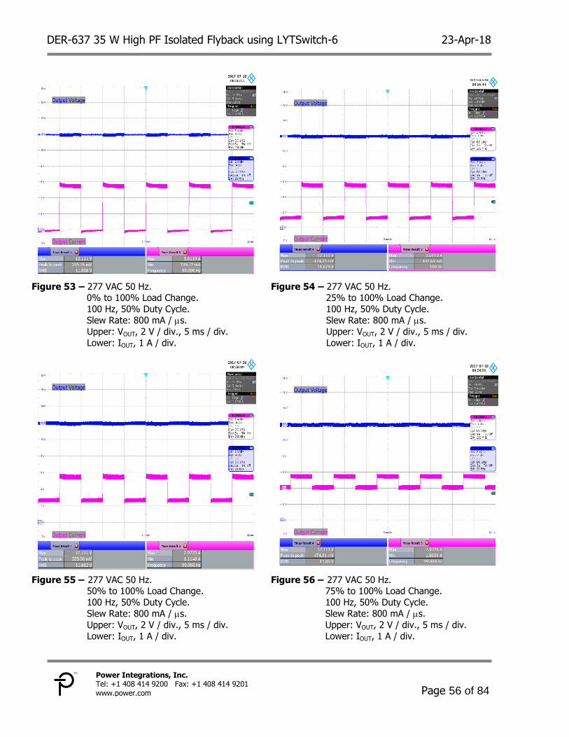
Upper: VOUT, 2 V / div., 5 ms / div.
Lower: IOUT, 1 A / div.
Figure 54 – 277 VAC 50 Hz. 25% to 100% Load Change.
100 Hz, 50% Duty Cycle.
Slew Rate: 800 mA / s.
Upper: VOUT, 2 V / div., 5 ms / div.
Lower: IOUT, 1 A / div.
Figure 55 – 277 VAC 50 Hz. 50% to 100% Load Change.
100 Hz, 50% Duty Cycle.
Slew Rate: 800 mA / s.
Upper: VOUT, 2 V / div., 5 ms / div.
Lower: IOUT, 1 A / div.
Figure 56 – 277 VAC 50 Hz. 75% to 100% Load Change.
100 Hz, 50% Duty Cycle.
Slew Rate: 800 mA / s.
Upper: VOUT, 2 V / div., 5 ms / div.
Lower: IOUT, 1 A / div.
23-Apr-18 DER-637 35 W High PF Isolated Flyback using LYTSwitch-6
Page 57 of 84
Power Integrations Tel: +1 408 414 9200 Fax: +1 408 414 9201
www.power.com
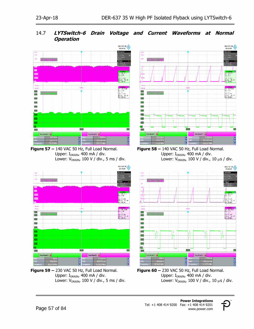
LYTSwitch-6 Drain Voltage and Current Waveforms at Normal 14.7Operation
Figure 57 – 140 VAC 50 Hz, Full Load Normal.
Upper: IDRAIN, 400 mA / div.
Lower: VDRAIN, 100 V / div., 5 ms / div.
Figure 58 – 140 VAC 50 Hz, Full Load Normal. Upper: IDRAIN, 400 mA / div.
Lower: VDRAIN, 100 V / div., 10 s / div.
Figure 59 – 230 VAC 50 Hz, Full Load Normal. Upper: IDRAIN, 400 mA / div.
Lower: VDRAIN, 100 V / div., 5 ms / div.
Figure 60 – 230 VAC 50 Hz, Full Load Normal. Upper: IDRAIN, 400 mA / div.
Lower: VDRAIN, 100 V / div., 10 s / div.

DER-637 35 W High PF Isolated Flyback using LYTSwitch-6 23-Apr-18
Page 58 of 84
Power Integrations, Inc. Tel: +1 408 414 9200 Fax: +1 408 414 9201 www.power.com
23-Apr-18 DER-637 35 W High PF Isolated Flyback using LYTSwitch-6
Page 59 of 84
Power Integrations Tel: +1 408 414 9200 Fax: +1 408 414 9201
www.power.com
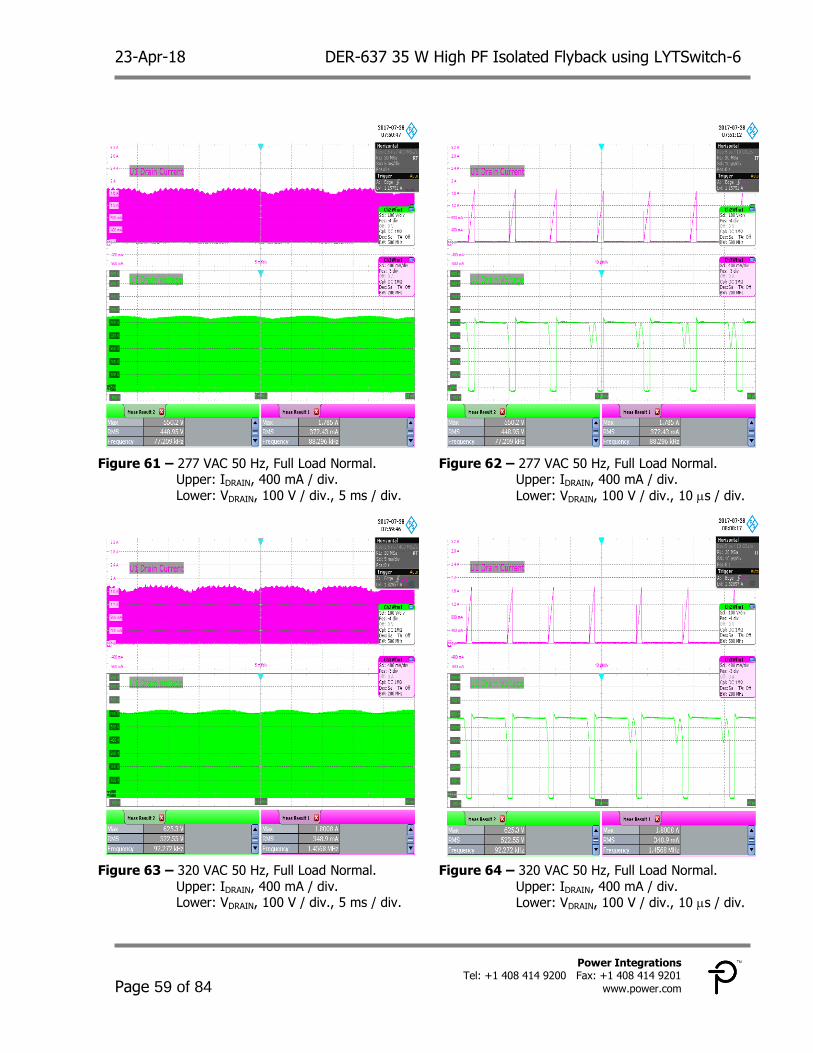
Figure 61 – 277 VAC 50 Hz, Full Load Normal.
Upper: IDRAIN, 400 mA / div.
Lower: VDRAIN, 100 V / div., 5 ms / div.
Figure 62 – 277 VAC 50 Hz, Full Load Normal. Upper: IDRAIN, 400 mA / div.
Lower: VDRAIN, 100 V / div., 10 s / div.
Figure 63 – 320 VAC 50 Hz, Full Load Normal.
Upper: IDRAIN, 400 mA / div. Lower: VDRAIN, 100 V / div., 5 ms / div.
Figure 64 – 320 VAC 50 Hz, Full Load Normal.
Upper: IDRAIN, 400 mA / div.
Lower: VDRAIN, 100 V / div., 10 s / div.
DER-637 35 W High PF Isolated Flyback using LYTSwitch-6 23-Apr-18
Page 60 of 84
Power Integrations, Inc. Tel: +1 408 414 9200 Fax: +1 408 414 9201 www.power.com
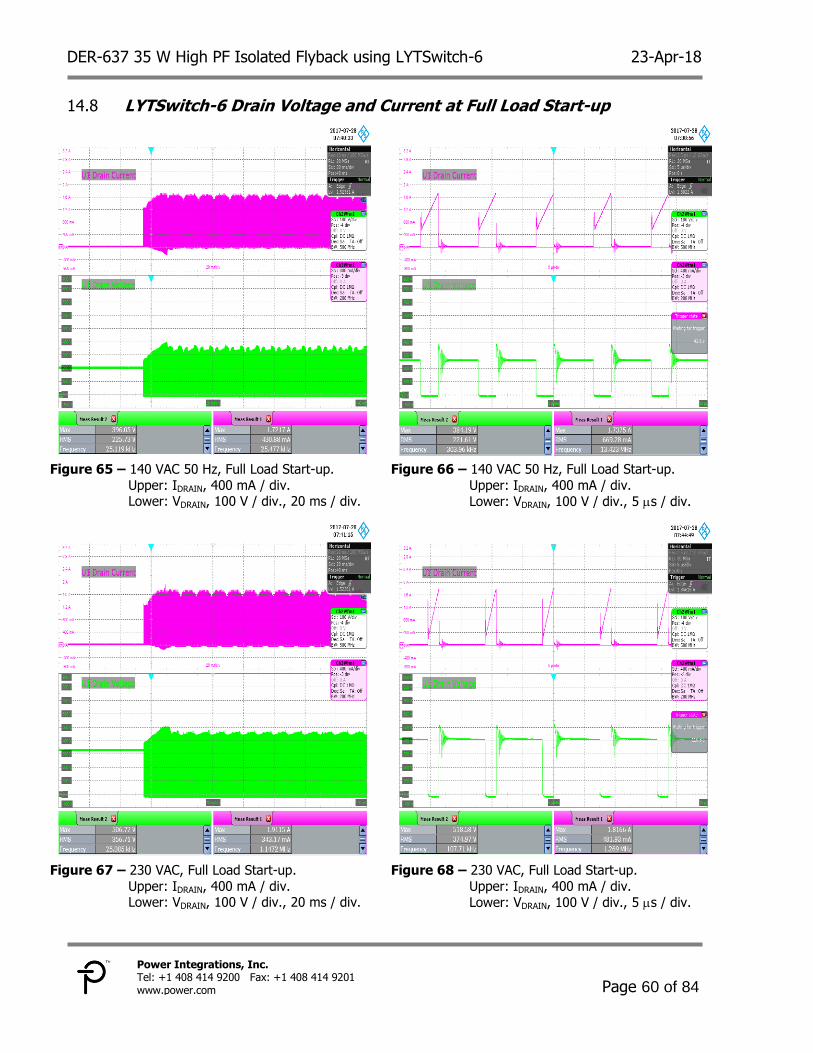
LYTSwitch-6 Drain Voltage and Current at Full Load Start-up 14.8
Figure 65 – 140 VAC 50 Hz, Full Load Start-up.
Upper: IDRAIN, 400 mA / div. Lower: VDRAIN, 100 V / div., 20 ms / div.
Figure 66 – 140 VAC 50 Hz, Full Load Start-up.
Upper: IDRAIN, 400 mA / div.
Lower: VDRAIN, 100 V / div., 5 s / div.
Figure 67 – 230 VAC, Full Load Start-up.
Upper: IDRAIN, 400 mA / div. Lower: VDRAIN, 100 V / div., 20 ms / div.
Figure 68 – 230 VAC, Full Load Start-up.
Upper: IDRAIN, 400 mA / div.
Lower: VDRAIN, 100 V / div., 5 s / div.
23-Apr-18 DER-637 35 W High PF Isolated Flyback using LYTSwitch-6
Page 61 of 84
Power Integrations Tel: +1 408 414 9200 Fax: +1 408 414 9201
www.power.com
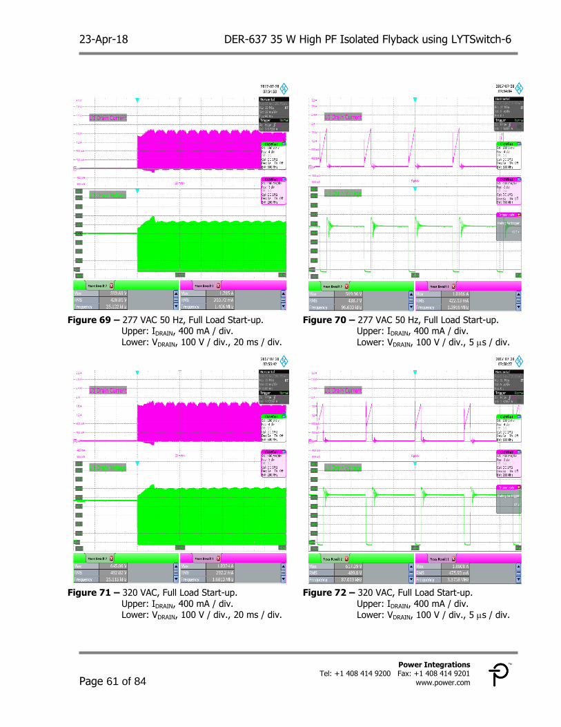
Figure 69 – 277 VAC 50 Hz, Full Load Start-up.
Upper: IDRAIN, 400 mA / div.
Lower: VDRAIN, 100 V / div., 20 ms / div.
Figure 70 – 277 VAC 50 Hz, Full Load Start-up. Upper: IDRAIN, 400 mA / div.
Lower: VDRAIN, 100 V / div., 5 s / div.
Figure 71 – 320 VAC, Full Load Start-up.
Upper: IDRAIN, 400 mA / div. Lower: VDRAIN, 100 V / div., 20 ms / div.
Figure 72 – 320 VAC, Full Load Start-up.
Upper: IDRAIN, 400 mA / div.
Lower: VDRAIN, 100 V / div., 5 s / div.
DER-637 35 W High PF Isolated Flyback using LYTSwitch-6 23-Apr-18
Page 62 of 84
Power Integrations, Inc. Tel: +1 408 414 9200 Fax: +1 408 414 9201 www.power.com
LYTSwitch-6 Drain Voltage and Current during Output Short-Circuit 14.9
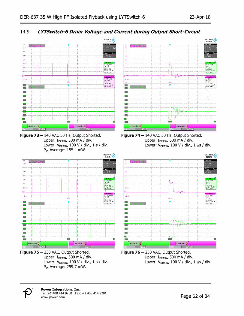
Figure 73 – 140 VAC 50 Hz, Output Shorted.
Upper: IDRAIN, 500 mA / div.
Lower: VDRAIN, 100 V / div., 1 s / div. PIN Average: 155.4 mW.
Figure 74 – 140 VAC 50 Hz, Output Shorted.
Upper: IDRAIN, 500 mA / div.
Lower: VDRAIN, 100 V / div., 1 s / div.
Figure 75 – 230 VAC, Output Shorted.
Upper: IDRAIN, 500 mA / div. Lower: VDRAIN, 100 V / div., 1 s / div.
PIN Average: 259.7 mW.
Figure 76 – 230 VAC, Output Shorted.
Upper: IDRAIN, 500 mA / div.
Lower: VDRAIN, 100 V / div., 1 s / div.
23-Apr-18 DER-637 35 W High PF Isolated Flyback using LYTSwitch-6
Page 63 of 84
Power Integrations Tel: +1 408 414 9200 Fax: +1 408 414 9201
www.power.com
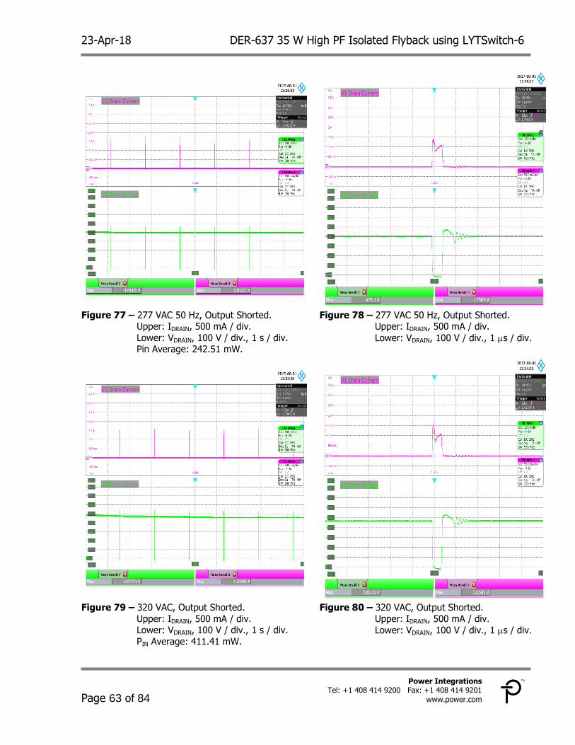
Figure 77 – 277 VAC 50 Hz, Output Shorted. Upper: IDRAIN, 500 mA / div.
Lower: VDRAIN, 100 V / div., 1 s / div. Pin Average: 242.51 mW.
Figure 78 – 277 VAC 50 Hz, Output Shorted. Upper: IDRAIN, 500 mA / div.
Lower: VDRAIN, 100 V / div., 1 s / div.
Figure 79 – 320 VAC, Output Shorted.
Upper: IDRAIN, 500 mA / div. Lower: VDRAIN, 100 V / div., 1 s / div.
PIN Average: 411.41 mW.
Figure 80 – 320 VAC, Output Shorted.
Upper: IDRAIN, 500 mA / div.
Lower: VDRAIN, 100 V / div., 1 s / div.
DER-637 35 W High PF Isolated Flyback using LYTSwitch-6 23-Apr-18
Page 64 of 84
Power Integrations, Inc. Tel: +1 408 414 9200 Fax: +1 408 414 9201 www.power.com
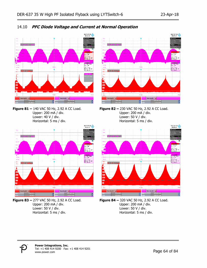
PFC Diode Voltage and Current at Normal Operation 14.10
Figure 81 – 140 VAC 50 Hz, 2.92 A CC Load.
Upper: 200 mA / div.
Lower: 40 V / div. Horizontal: 5 ms / div.
Figure 82 – 230 VAC 50 Hz, 2.92 A CC Load.
Upper: 200 mA / div.
Lower: 50 V / div. Horizontal: 5 ms / div.
Figure 83 – 277 VAC 50 Hz, 2.92 A CC Load. Upper: 200 mA / div.
Lower: 50 V / div. Horizontal: 5 ms / div.
Figure 84 – 320 VAC 50 Hz, 2.92 A CC Load. Upper: 200 mA / div.
Lower: 50 V / div. Horizontal: 5 ms / div.
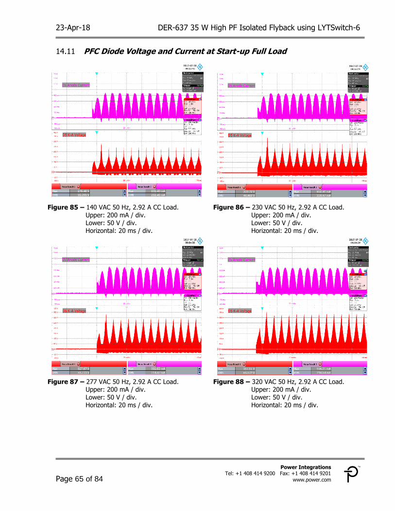
23-Apr-18 DER-637 35 W High PF Isolated Flyback using LYTSwitch-6
Page 65 of 84
Power Integrations Tel: +1 408 414 9200 Fax: +1 408 414 9201
www.power.com
PFC Diode Voltage and Current at Start-up Full Load 14.11
Figure 85 – 140 VAC 50 Hz, 2.92 A CC Load.
Upper: 200 mA / div.
Lower: 50 V / div. Horizontal: 20 ms / div.
Figure 86 – 230 VAC 50 Hz, 2.92 A CC Load.
Upper: 200 mA / div.
Lower: 50 V / div. Horizontal: 20 ms / div.
Figure 87 – 277 VAC 50 Hz, 2.92 A CC Load. Upper: 200 mA / div.
Lower: 50 V / div. Horizontal: 20 ms / div.
Figure 88 – 320 VAC 50 Hz, 2.92 A CC Load. Upper: 200 mA / div.
Lower: 50 V / div. Horizontal: 20 ms / div.
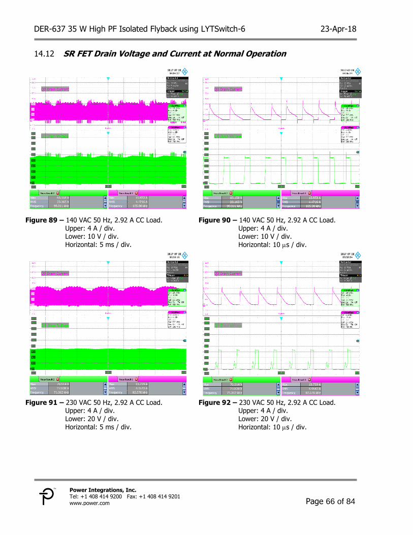
DER-637 35 W High PF Isolated Flyback using LYTSwitch-6 23-Apr-18
Page 66 of 84
Power Integrations, Inc. Tel: +1 408 414 9200 Fax: +1 408 414 9201 www.power.com
SR FET Drain Voltage and Current at Normal Operation 14.12
Figure 89 – 140 VAC 50 Hz, 2.92 A CC Load.
Upper: 4 A / div. Lower: 10 V / div.
Horizontal: 5 ms / div.
Figure 90 – 140 VAC 50 Hz, 2.92 A CC Load.
Upper: 4 A / div. Lower: 10 V / div.
Horizontal: 10 s / div.
Figure 91 – 230 VAC 50 Hz, 2.92 A CC Load. Upper: 4 A / div.
Lower: 20 V / div.
Horizontal: 5 ms / div.
Figure 92 – 230 VAC 50 Hz, 2.92 A CC Load. Upper: 4 A / div.
Lower: 20 V / div.
Horizontal: 10 s / div.
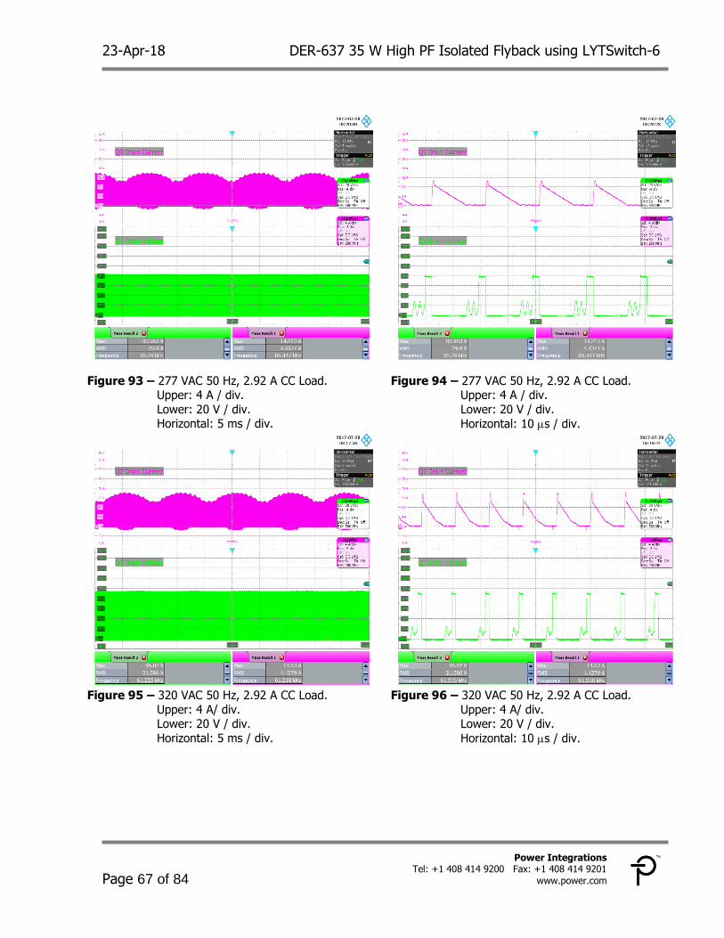
23-Apr-18 DER-637 35 W High PF Isolated Flyback using LYTSwitch-6
Page 67 of 84
Power Integrations Tel: +1 408 414 9200 Fax: +1 408 414 9201
www.power.com
Figure 93 – 277 VAC 50 Hz, 2.92 A CC Load. Upper: 4 A / div.
Lower: 20 V / div. Horizontal: 5 ms / div.
Figure 94 – 277 VAC 50 Hz, 2.92 A CC Load. Upper: 4 A / div.
Lower: 20 V / div.
Horizontal: 10 s / div.
Figure 95 – 320 VAC 50 Hz, 2.92 A CC Load.
Upper: 4 A/ div. Lower: 20 V / div.
Horizontal: 5 ms / div.
Figure 96 – 320 VAC 50 Hz, 2.92 A CC Load.
Upper: 4 A/ div. Lower: 20 V / div.
Horizontal: 10 s / div.
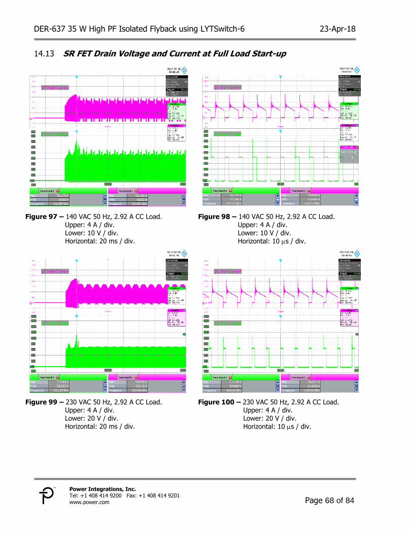
DER-637 35 W High PF Isolated Flyback using LYTSwitch-6 23-Apr-18
Page 68 of 84
Power Integrations, Inc. Tel: +1 408 414 9200 Fax: +1 408 414 9201 www.power.com
SR FET Drain Voltage and Current at Full Load Start-up 14.13
Figure 97 – 140 VAC 50 Hz, 2.92 A CC Load.
Upper: 4 A / div.
Lower: 10 V / div. Horizontal: 20 ms / div.
Figure 98 – 140 VAC 50 Hz, 2.92 A CC Load.
Upper: 4 A / div.
Lower: 10 V / div.
Horizontal: 10 s / div.
Figure 99 – 230 VAC 50 Hz, 2.92 A CC Load. Upper: 4 A / div.
Lower: 20 V / div. Horizontal: 20 ms / div.
Figure 100 – 230 VAC 50 Hz, 2.92 A CC Load. Upper: 4 A / div.
Lower: 20 V / div.
Horizontal: 10 s / div.
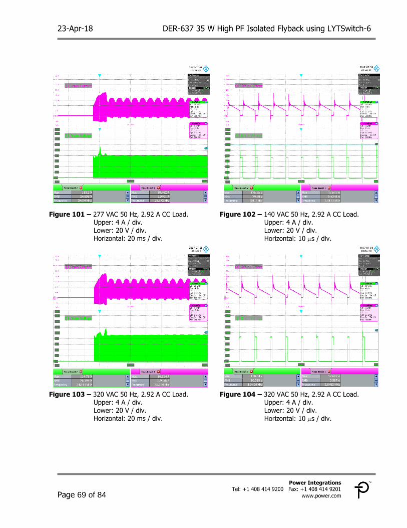
23-Apr-18 DER-637 35 W High PF Isolated Flyback using LYTSwitch-6
Page 69 of 84
Power Integrations Tel: +1 408 414 9200 Fax: +1 408 414 9201
www.power.com
Figure 101 – 277 VAC 50 Hz, 2.92 A CC Load. Upper: 4 A / div.
Lower: 20 V / div. Horizontal: 20 ms / div.
Figure 102 – 140 VAC 50 Hz, 2.92 A CC Load. Upper: 4 A / div.
Lower: 20 V / div.
Horizontal: 10 s / div.
Figure 103 – 320 VAC 50 Hz, 2.92 A CC Load. Upper: 4 A / div.
Lower: 20 V / div. Horizontal: 20 ms / div.
Figure 104 – 320 VAC 50 Hz, 2.92 A CC Load. Upper: 4 A / div.
Lower: 20 V / div.
Horizontal: 10 s / div.
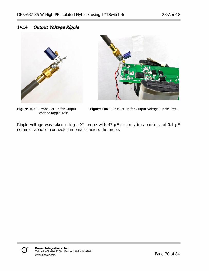
DER-637 35 W High PF Isolated Flyback using LYTSwitch-6 23-Apr-18
Page 70 of 84
Power Integrations, Inc. Tel: +1 408 414 9200 Fax: +1 408 414 9201 www.power.com
Output Voltage Ripple 14.14
Figure 105 – Probe Set-up for Output
Voltage Ripple Test.
Figure 106 – Unit Set-up for Output Voltage Ripple Test.
Ripple voltage was taken using a X1 probe with 47 F electrolytic capacitor and 0.1 F
ceramic capacitor connected in parallel across the probe.
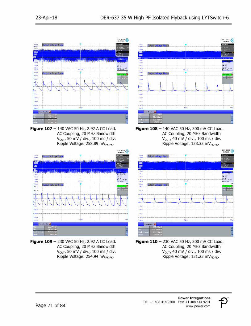
23-Apr-18 DER-637 35 W High PF Isolated Flyback using LYTSwitch-6
Page 71 of 84
Power Integrations Tel: +1 408 414 9200 Fax: +1 408 414 9201
www.power.com
Figure 107 – 140 VAC 50 Hz, 2.92 A CC Load. AC Coupling, 20 MHz Bandwidth
VOUT, 50 mV / div., 100 ms / div. Ripple Voltage: 258.89 mVPK-PK.
Figure 108 – 140 VAC 50 Hz, 300 mA CC Load. AC Coupling, 20 MHz Bandwidth
VOUT, 40 mV / div., 100 ms / div. Ripple Voltage: 123.32 mVPK-PK.
Figure 109 – 230 VAC 50 Hz, 2.92 A CC Load. AC Coupling, 20 MHz Bandwidth
VOUT, 50 mV / div., 100 ms / div. Ripple Voltage: 254.94 mVPK-PK.
Figure 110 – 230 VAC 50 Hz, 300 mA CC Load. AC Coupling, 20 MHz Bandwidth
VOUT, 40 mV / div., 100 ms / div. Ripple Voltage: 131.23 mVPK-PK.
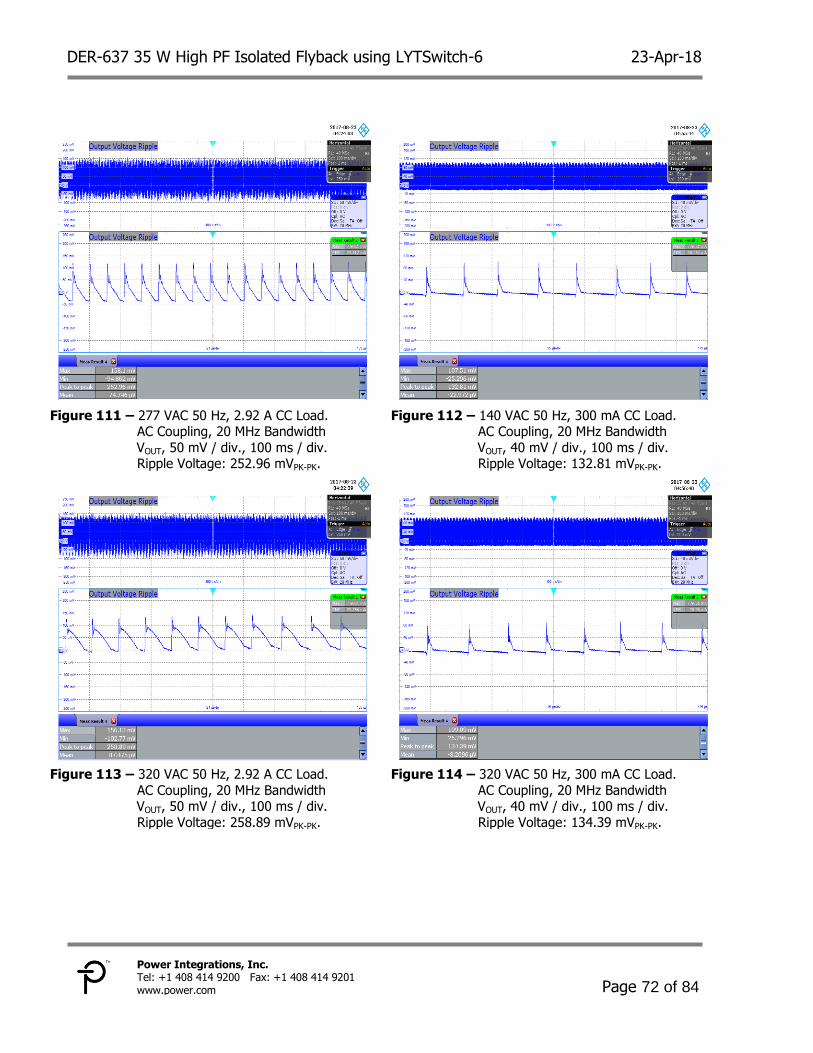
DER-637 35 W High PF Isolated Flyback using LYTSwitch-6 23-Apr-18
Page 72 of 84
Power Integrations, Inc. Tel: +1 408 414 9200 Fax: +1 408 414 9201 www.power.com
Figure 111 – 277 VAC 50 Hz, 2.92 A CC Load. AC Coupling, 20 MHz Bandwidth
VOUT, 50 mV / div., 100 ms / div. Ripple Voltage: 252.96 mVPK-PK.
Figure 112 – 140 VAC 50 Hz, 300 mA CC Load. AC Coupling, 20 MHz Bandwidth
VOUT, 40 mV / div., 100 ms / div. Ripple Voltage: 132.81 mVPK-PK.
Figure 113 – 320 VAC 50 Hz, 2.92 A CC Load.
AC Coupling, 20 MHz Bandwidth VOUT, 50 mV / div., 100 ms / div.
Ripple Voltage: 258.89 mVPK-PK.
Figure 114 – 320 VAC 50 Hz, 300 mA CC Load.
AC Coupling, 20 MHz Bandwidth VOUT, 40 mV / div., 100 ms / div.
Ripple Voltage: 134.39 mVPK-PK.
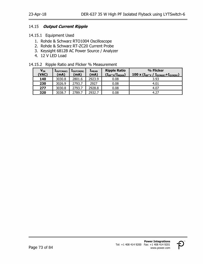
23-Apr-18 DER-637 35 W High PF Isolated Flyback using LYTSwitch-6
Page 73 of 84
Power Integrations Tel: +1 408 414 9200 Fax: +1 408 414 9201
www.power.com
Output Current Ripple 14.15
Equipment Used 14.15.1
1. Rohde & Schwarz RTO1004 Oscilloscope 2. Rohde & Schwarz RT-ZC20 Current Probe 3. Keysight 6812B AC Power Source / Analyzer 4. 12 V LED Load
Ripple Ratio and Flicker % Measurement 14.15.2
VIN
(VAC)
IOUT(MAX)
(mA)
IOUT(MIN)
(mA)
IMEAN
(mA)
Ripple Ratio
(IRP-P/IMEAN)
% Flicker
100 x (IRP-P / IO(MAX)+IO(MIN))
140 3030.8 2801.6 2923.9 0.08 3.93
230 3026.9 2793.7 2927 0.08 4.01
277 3030.8 2793.7 2928.8 0.08 4.07
320 3038.7 2789.7 2932.7 0.08 4.27
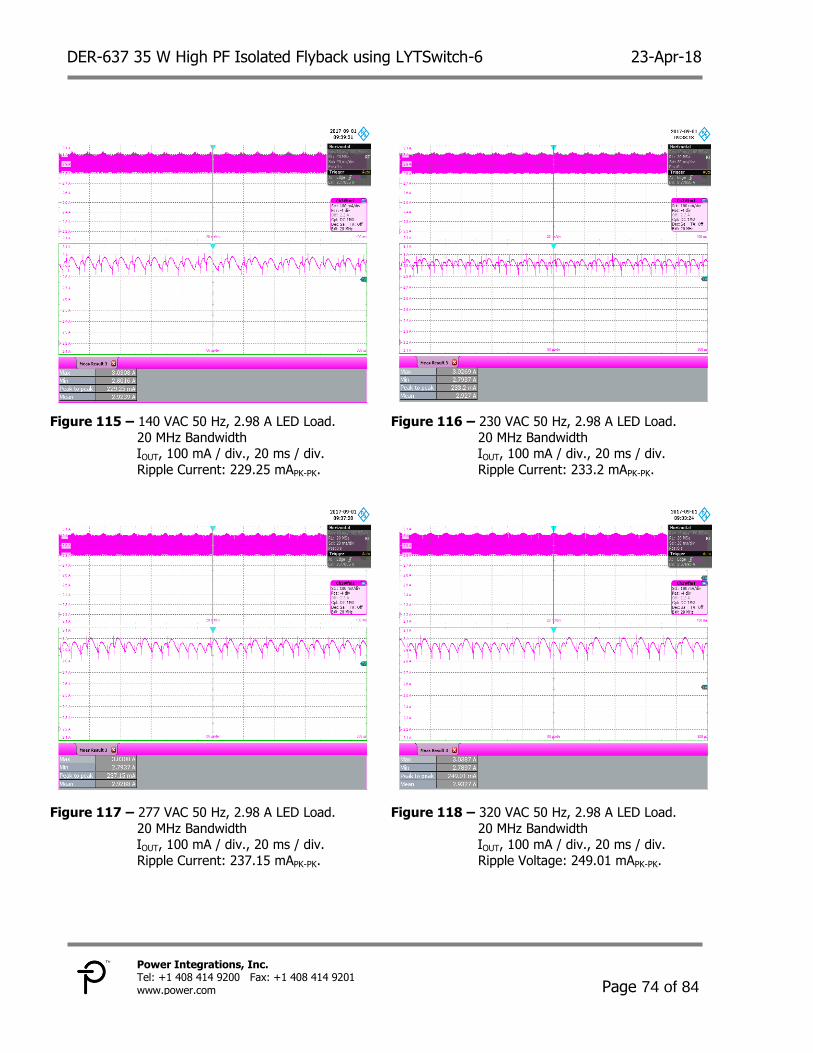
DER-637 35 W High PF Isolated Flyback using LYTSwitch-6 23-Apr-18
Page 74 of 84
Power Integrations, Inc. Tel: +1 408 414 9200 Fax: +1 408 414 9201 www.power.com
Figure 115 – 140 VAC 50 Hz, 2.98 A LED Load.
20 MHz Bandwidth IOUT, 100 mA / div., 20 ms / div.
Ripple Current: 229.25 mAPK-PK.
Figure 116 – 230 VAC 50 Hz, 2.98 A LED Load.
20 MHz Bandwidth IOUT, 100 mA / div., 20 ms / div.
Ripple Current: 233.2 mAPK-PK.
Figure 117 – 277 VAC 50 Hz, 2.98 A LED Load.
20 MHz Bandwidth IOUT, 100 mA / div., 20 ms / div.
Ripple Current: 237.15 mAPK-PK.
Figure 118 – 320 VAC 50 Hz, 2.98 A LED Load.
20 MHz Bandwidth IOUT, 100 mA / div., 20 ms / div.
Ripple Voltage: 249.01 mAPK-PK.
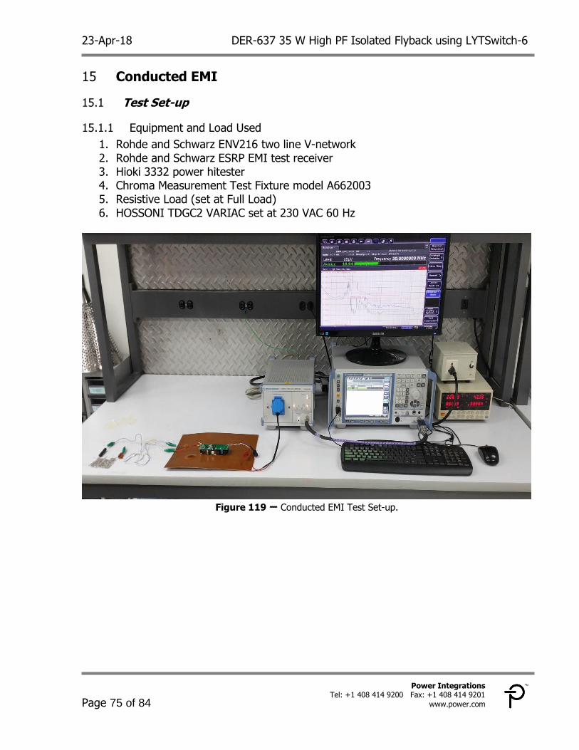
23-Apr-18 DER-637 35 W High PF Isolated Flyback using LYTSwitch-6
Page 75 of 84
Power Integrations Tel: +1 408 414 9200 Fax: +1 408 414 9201
www.power.com
Conducted EMI 15
Test Set-up 15.1
Equipment and Load Used 15.1.1
1. Rohde and Schwarz ENV216 two line V-network 2. Rohde and Schwarz ESRP EMI test receiver 3. Hioki 3332 power hitester 4. Chroma Measurement Test Fixture model A662003 5. Resistive Load (set at Full Load) 6. HOSSONI TDGC2 VARIAC set at 230 VAC 60 Hz
Figure 119 – Conducted EMI Test Set-up.
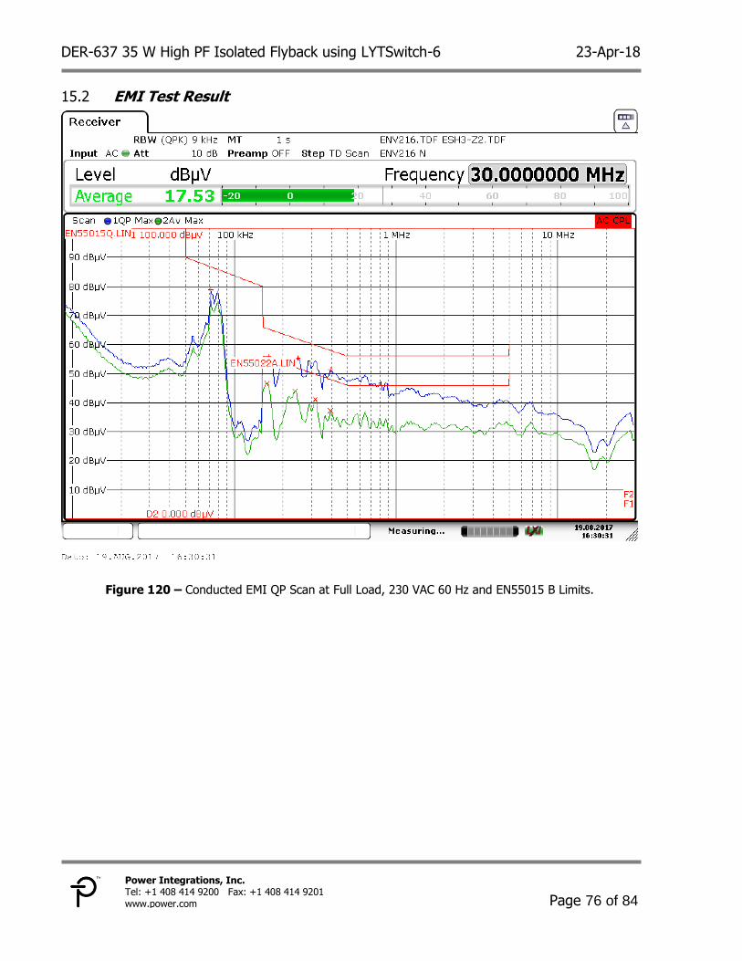
DER-637 35 W High PF Isolated Flyback using LYTSwitch-6 23-Apr-18
Page 76 of 84
Power Integrations, Inc. Tel: +1 408 414 9200 Fax: +1 408 414 9201 www.power.com
EMI Test Result 15.2
Figure 120 – Conducted EMI QP Scan at Full Load, 230 VAC 60 Hz and EN55015 B Limits.
23-Apr-18 DER-637 35 W High PF Isolated Flyback using LYTSwitch-6
Page 77 of 84
Power Integrations Tel: +1 408 414 9200 Fax: +1 408 414 9201
www.power.com
Figure 121 – Conducted EMI Data at 230 VAC 60 Hz, Full Load
DER-637 35 W High PF Isolated Flyback using LYTSwitch-6 23-Apr-18
Page 78 of 84
Power Integrations, Inc. Tel: +1 408 414 9200 Fax: +1 408 414 9201 www.power.com
Line Surge 16
The unit was subjected to ±2500 V, 100 kHz ring wave and ±1000 V differential surge using 10 strikes at each condition. A test failure was defined as a non-recoverable interruption of output requiring repair or recycling of input voltage.
Figure 122 – Test Set-up for Line Surge Test.
23-Apr-18 DER-637 35 W High PF Isolated Flyback using LYTSwitch-6
Page 79 of 84
Power Integrations Tel: +1 408 414 9200 Fax: +1 408 414 9201
www.power.com
Differential Surge Test Results 16.1
Surge
Level (V)
Input
Voltage (VAC)
Injection
Location
Injection
Phase (°)
Test Result
(Pass/Fail)
+1000 230 L to N 0 Pass
-1000 230 L to N 0 Pass
+1000 230 L to N 90 Pass
-1000 230 L to N 90 Pass
+1000 230 L to N 270 Pass
-1000 230 L to N 270 Pass
+1000 277 L to N 0 Pass
-1000 277 L to N 0 Pass
+1000 277 L to N 90 Pass
-1000 277 L to N 90 Pass
+1000 277 L to N 270 Pass
-1000 277 L to N 270 Pass
Ring Wave Surge Test Results 16.2
Surge
Level (V)
Input Voltage
(VAC)
Injection
Location
Injection
Phase (°)
Test Result
(Pass/Fail)
+2500 230 L to N 0 Pass
-2500 230 L to N 0 Pass
+2500 230 L to N 90 Pass
-2500 230 L to N 90 Pass
+2500 230 L to N 270 Pass
-2500 230 L to N 270 Pass
+2500 277 L to N 0 Pass
-2500 277 L to N 0 Pass
+2500 277 L to N 90 Pass
-2500 277 L to N 90 Pass
+2500 277 L to N 270 Pass
-2500 277 L to N 270 Pass
DER-637 35 W High PF Isolated Flyback using LYTSwitch-6 23-Apr-18
Page 80 of 84
Power Integrations, Inc. Tel: +1 408 414 9200 Fax: +1 408 414 9201 www.power.com
1 kV Differential Surge Test 16.3
The Drain voltage of U1-LYTSwitch-6 was measured during 1 kV differential surge test.
Figure 123 – (+)1 kV Differential Surge.
90º Phase Angle, Input: 277 VAC. VDRAIN, 200 V / div., 20 ms / div.
Peak VDRAIN: 595.833 V.
Figure 124 – (-)1 kV Differential Surge.
90º Phase Angle, Input: 277 VAC. VDRAIN, 200 V / div., 20 ms / div.
Peak VDRAIN: 583.333 V.
Figure 125 – (+)1 kV Differential Surge.
270º Phase Angle, Input: 277 VAC. VDRAIN, 200 V / div., 20 ms / div.
Peak VDRAIN: 587.5 V.
Figure 126 – (-)1 kV Differential Surge.
270º Phase Angle, Input: 277 VAC. VDRAIN, 200 V / div., 20 ms / div.
Peak VDRAIN: 591.667 V.
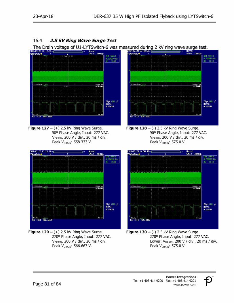
23-Apr-18 DER-637 35 W High PF Isolated Flyback using LYTSwitch-6
Page 81 of 84
Power Integrations Tel: +1 408 414 9200 Fax: +1 408 414 9201
www.power.com
2.5 kV Ring Wave Surge Test 16.4
The Drain voltage of U1-LYTSwitch-6 was measured during 2 kV ring wave surge test.
Figure 127 – (+) 2.5 kV Ring Wave Surge.
90º Phase Angle, Input: 277 VAC. VDRAIN, 200 V / div., 20 ms / div.
Peak VDRAIN: 558.333 V.
Figure 128 – (-) 2.5 kV Ring Wave Surge.
90º Phase Angle, Input: 277 VAC. VDRAIN, 200 V / div., 20 ms / div.
Peak VDRAIN: 575.0 V.
Figure 129 – (+) 2.5 kV Ring Wave Surge. 270º Phase Angle, Input: 277 VAC.
VDRAIN, 200 V / div., 20 ms / div. Peak VDRAIN: 566.667 V.
Figure 130 – (-) 2.5 kV Ring Wave Surge. 270º Phase Angle, Input: 277 VAC.
Lower: VDRAIN, 200 V / div., 20 ms / div. Peak VDRAIN: 575.0 V.
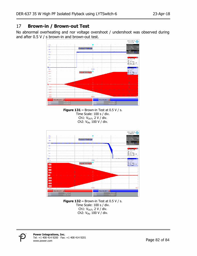
DER-637 35 W High PF Isolated Flyback using LYTSwitch-6 23-Apr-18
Page 82 of 84
Power Integrations, Inc. Tel: +1 408 414 9200 Fax: +1 408 414 9201 www.power.com
Brown-in / Brown-out Test 17
No abnormal overheating and nor voltage overshoot / undershoot was observed during and after 0.5 V / s brown-in and brown-out test.
Figure 131 – Brown-in Test at 0.5 V / s.
Time Scale: 100 s / div. Ch1: VOUT, 2 V / div.
Ch2: VIN, 100 V / div.
Figure 132 – Brown-in Test at 0.5 V / s.
Time Scale: 100 s / div. Ch1: VOUT, 2 V / div.
Ch2: VIN, 100 V / div.
23-Apr-18 DER-637 35 W High PF Isolated Flyback using LYTSwitch-6
Page 83 of 84
Power Integrations Tel: +1 408 414 9200 Fax: +1 408 414 9201
www.power.com
Revision History 18
Date Author Revision Description and Changes Reviewed
23-Jan-18 EDdL 1.0 Initial Release. Apps & Mktg
16-Feb-18 EDdL 1.1 Minor Text Updates. PCB Images Updated.
21-Feb-18 EDdl 1.2 Added PIXls Spreadsheet.
26-Mar-18 EDdl 1.3 Updated Power Supply Specification, Section 2.0.
23-Apr-18 KCM 1.4 Updated Figure 4 Schematic.

DER-637 35 W High PF Isolated Flyback using LYTSwitch-6 23-Apr-18
Page 84 of 84
Power Integrations, Inc. Tel: +1 408 414 9200 Fax: +1 408 414 9201 www.power.com
Recommended