Asian Journal of Convergence in Technology Volume IV Issue II
ISSN NO: 2350-1146 I.F-5.11
www.asianssr.org Page 1
Design and Implementation of Z-source inverter
using SBC
Mrudul A. Mawlikar
M.E. Power Electronics and Drives
Department of Electrical Engineering
Fr.C.Rodrigues Institute of Technology,
Navi Mumbai, Maharashtra, India.
Ms. Sreedevi S Nair
Assistant Professor
Department of Electrical Engineering
Fr.C.Rodrigues Institute of Technology,
Navi Mumbai, Maharashtra, India.
Abstract— This paper presents a comprehensive
design and hardware implementation of Z-source
inverter. For most of the renewable applications, the
conventional VSI has been used which requires an
additional boost converter to boost the output
voltage. Z-source inverter provides a single stage
power conversion topology which can give both
voltage buck and boost properties. The control
method used in the Z-source inverter is the Simple
Boost Control (SBC) technique with Sinusoidal pulse
width modulation. The design of the impedance
network, hardware results of single stage Z-source
inverter are presented in this paper.
Keywords—Z-source inverter, SBC.
I. INTRODUCTION
Traditional inverters are categorised into two types namely Voltage Source Inverters (VSI) and the Current Source Inverters (CSI). VSI is a single phase or a three phase bridge inverter fed from a DC voltage source such as a battery or an AC voltage source with a diode rectifier circuit. The AC output voltage of a VSI doesn’t exceed the DC input voltage. In many applications where renewable energy sources such as PV, Fuel cell is used, the input DC voltage is not always constant. In such cases a DC/DC boost converter is utilized to boost the DC input voltage to meet the required AC output voltage. This increases the system cost and complexity.[1][2]
The VSI has a disadvantage that the two switches of the same leg cannot be gated on at the
same time. This is expressed as Shoot through state, which will destroy the inverter. A dead time is introduced to avoid switching ON of two switches in the same leg simultaneously. This results into harmonic issues and output voltage distortion.
Likewise, in a CSI, the DC current at the input is maintained constant with a small ripple by using a large inductor fed from a voltage source. The output voltage of a CSI is greater than the DC input voltage. In a single phase CSI, at least one of the upper switches and one of the lower switches should be maintained on at any time. Else, an open circuit problem occurs which destroys the inverter. Also to have reverse blocking capability, a series diode is used in combination with the switches of the inverter.
The traditional inverters have a limitation that
they can have either buck or boost operation only.
Open or short circuit conditions result in the
damage of the devices. To overcome the problems
associated with the traditional VSI and CSI, an
impedance source inverter or Z-source inverter is
presented in this paper. This methodology was first
proposed by F.Z.Peng in the year 2002[1]. Z-
source inverter operates as a buck-boost inverter
without using the DC-DC converter bridge due to
its unique circuit topology.
Z-source inverter utilises a LC impedance network for coupling the inverter circuit to the power source. It also allows the use of shoot through switching states, which eliminates the need

Asian Journal of Convergence in Technology Volume IV Issue II
ISSN NO: 2350-1146 I.F-5.11
www.asianssr.org Page 2
for dead times that are used in traditional inverters. The Z-source inverter consists of two inductors L1
and L2 and two capacitors C1 and C2 connected in an X shape.[3]
This paper presents a comprehensive design and hardware implementation of a single phase Z-source inverter. In most PV applications, since the PV output voltage is low, a two stage conversion topology is used as shown in Fig.1. First the PV voltage is boosted to the required DC output voltage by a boost converter, which is then converted to an AC voltage by using a single phase VSI. The input voltage Vdc could be provided by solar panel.
Fig: 1. Z-source Inverter used for PV applications
Fig: 1 represents the Z-source inverter implemented for such applications. Z-source inverter can straightaway produce an AC output voltage greater or less than the input PV voltage. The input diode D1 is reverse blocking diode used to prevent the reverse current flow to the source.
II. Z SOURCE INVERTER
A. Working Principle
The Z source inverter is established on the Z
source network which can be used to buck or boost
the input DC voltage. It utilizes the forbidden state
(inverter shorted state) for the buck and boost of the
input voltage. The concept of boosting the input
voltage is based on the ratio of ‘shoot through’ time
to the whole switching period. The impedance
network consists of capacitors C1, C2 and inductors
L1, L2 connected in X shape to provide an
impedance source coupling the inverter to DC
source. The inductors are responsible for
eliminating the inrush current and harmonics of the
current waveform. It forms a second order filter and
handles undesirable voltage sags of the DC source.
The Z source concept can be applied to all AC-AC,
DC-DC, DC-AC and AC-DC conversion. The
circuit diagram of a single phase Z-source inverter
is shown in Fig:2.[1][4]
Fig. 2. Z source inverter
In single phase Z source inverter, an additional
control parameter is introduced namely the Boost
factor (B), which modifies the AC output voltage of
traditional 1-phase PWM inverter as shown in
“(1)”.[1][4]
Vout = BMVDC (1)
Vout is maximum sinusoidal voltage
B is boost factor
M is modulation index
VDC is input voltage
The gain of the inverter is given by G where
G=BM.
For a single phase traditional inverter, the AC
output voltage is given by “(2)”.[1][4]
Vout = MVDC (2)
The inverter gain can be expressed as G = BM
The modulation index also called as amplitude
modulation ratio (M) is defined as ratio of

Asian Journal of Convergence in Technology Volume IV Issue II
ISSN NO: 2350-1146 I.F-5.11
www.asianssr.org Page 3
amplitude of reference wave to the amplitude of
carrier wave as shown in “(3)”.[1][4]
M = 𝑉𝑟𝑒𝑓
𝑉𝑐𝑎𝑟 (3)
The shoot through duty ratio is given by “(4)”
D0 = 𝑇0
𝑇 (4)
where T0 is shoot through interval and
T is switching period
The boost factor is resulting from the shoot
through state which is introduced for a short period
of time in one complete switching cycle and is
expressed by “(5)”.[1][4]
B = 1
1−2𝐷0 (5)
B. Modes of operation of Z source inverter
The operation of Z source inverter can be
separated into three states namely: Active, Zero and
Shoot through state as shown in Table 1.[4]
TABLE 1. Switching states of Z-source inverter
Switching
states
S1 S2 S3 S4
Active
state
1 0 0 1
0 1 1 0
Zero state 1 0 1 0
0 1 0 1
Shoot
through
state
1 1 S3 S4
S1 S2 1 1
1 1 1 1
Z source inverters are implemented with the
view of boosting the voltage by utilizing the
forbidden shoot through state in the traditional
inverters. The impedance network is assumed to be
symmetrical which gives us
C1=C2=C and L1=L2=L
Voltage across inductors and capacitors is given as
VL1=VC1, VL2=VC2
1. Active state
This state represents the operation of inverter in
one of traditional active states where inverter bridge
acts as a current source viewed from the DC link.[4]
2. Zero state
This state represents the operation of inverter in
one of the traditional zero state where the inverter is
open circuited as viewed from Z source circuit. This
occurs due to switching of either both the upper
devices or both the lower devices in inverter leg.[4]
3. Shoot through state
This state represents the operation in the
forbidden state. This mode is incorporated in every
switching cycle during traditional zero vector period
generated by PWM control. Depending on the
voltage boost needed, the shoot through interval
(T0) or its duty cycle (T0/T) is determined.[4]
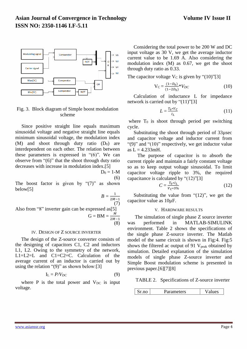
III. SIMPLE BOOST CONTROL
There are different modulation techniques for
controlling the z-source inverter. The modulation
techniques are classified based on the different
shoot through states insertion methods. One of the
simplest modulation scheme employed is the
Simple Boost Control (SBC) technique where z-
source inverter is used in the boost mode. This
control strategy maintains the seven states shown in
table and are unchanged as in traditional carrier
based PWM. Two straight lines are employed to
comprehend shoot through duty ratio (D0). The first
straight line is equal to the positive peak value of
sinusoidal reference voltage while the second is
equal to the negative peak value. When the
triangular carrier signal is greater than positive
straight line or smaller than the negative straight
line, the inverter operates in shoot through or else it
operates as traditional PWM inverter. The block
diagram used for implementing simple boost control
technique is shown in Fig.3.[5]
Asian Journal of Convergence in Technology Volume IV Issue II
ISSN NO: 2350-1146 I.F-5.11
www.asianssr.org Page 4
Fig. 3. Block diagram of Simple boost modulation
scheme
Since positive straight line equals maximum
sinusoidal voltage and negative straight line equals
minimum sinusoidal voltage, the modulation index
(M) and shoot through duty ratio (D0) are
interdependent on each other. The relation between
these parameters is expressed in “(6)”. We can
observe from “(6)” that the shoot through duty ratio
decreases with increase in modulation index.[5]
D0 = 1-M
(6)
The boost factor is given by “(7)” as shown
below[5]
B = 1
2𝑀−1
(7)
Also from “8” inverter gain can be expressed as[5]
G = BM = 𝑀
2𝑀−1
(8)
IV. DESIGN OF Z SOURCE INVERTER
The design of the Z-source converter consists of the designing of capacitors C1, C2 and inductors L1, L2. Owing to the symmetry of the network, L1=L2=L and C1=C2=C. Calculation of the average current of an inductor is carried out by using the relation “(9)” as shown below:[3]
IL = P/VDC (9)
where P is the total power and VDC is input voltage.
Considering the total power to be 200 W and DC input voltage as 30 V, we get the average inductor current value to be 1.69 A. Also considering the modulation index (M) as 0.67, we get the shoot through duty ratio as 0.33.
The capacitor voltage VC is given by “(10)”[3]
VC = (1−𝐷0)
(1−2𝐷0)*VDC (10)
Calculation of inductance L for impedance network is carried out by “(11)”[3]
L = 𝑇0∗𝑉𝐶
𝐼𝐿 (11)
where T0 is shoot through period per switching
cycle.
Substituting the shoot through period of 33µsec
and capacitor voltage and inductor current from
“(9)” and “(10)” respectively, we get inductor value
as L = 4.233mH.
The purpose of capacitor is to absorb the
current ripple and maintain a fairly constant voltage
so as to keep output voltage sinusoidal. To limit
capacitor voltage ripple to 3%, the required
capacitance is calculated by “(12)”[3]
C = 𝑇0∗𝐼𝐿
𝑉𝐶∗3% (12)
Substituting the value from “(12)”, we get the capacitor value as 10µF.
V. HARDWARE RESULTS
The simulation of single phase Z source inverter
was performed in MATLAB-SIMULINK
environment. Table 2 shows the specifications of
the single phase Z-source inverter. The Matlab
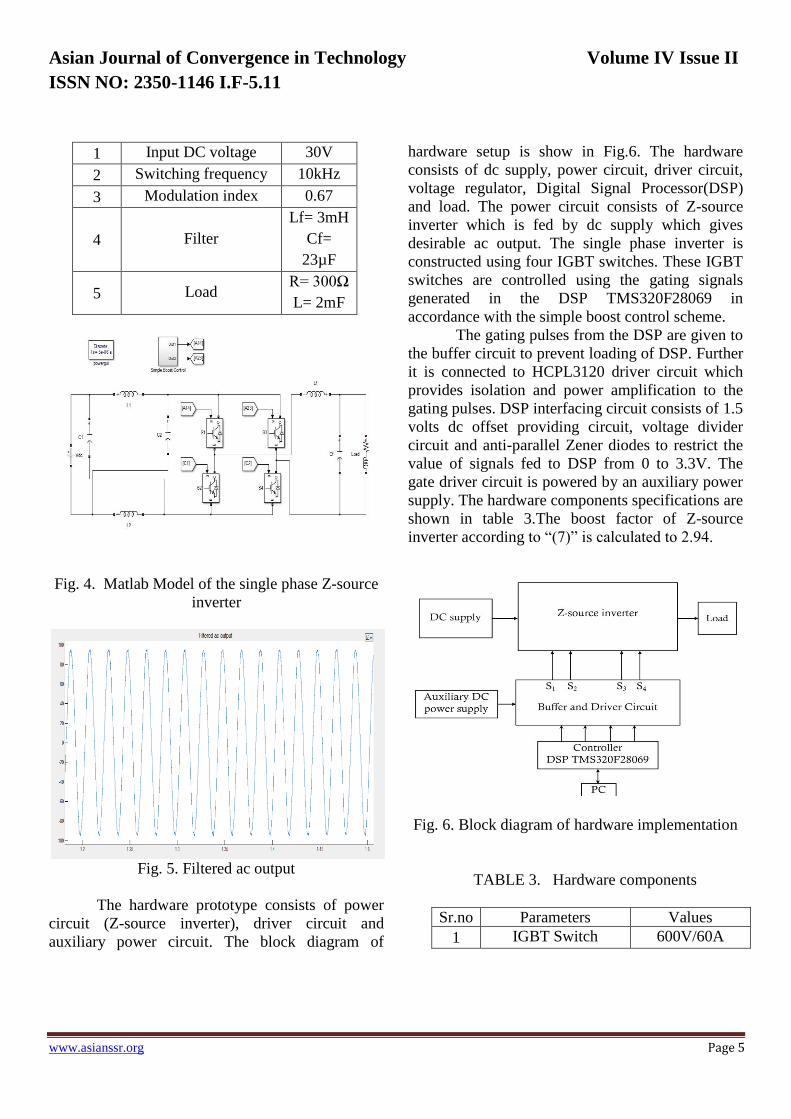
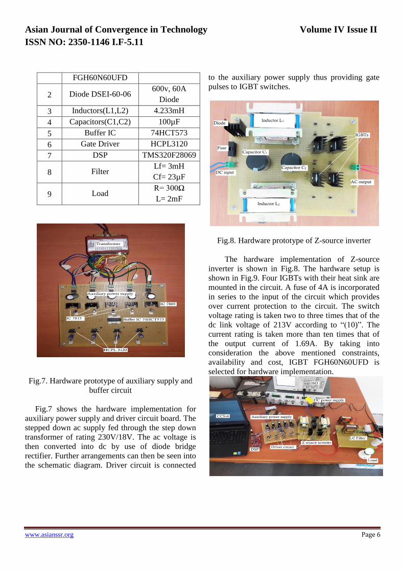
model of the same circuit is shown in Fig:4. Fig:5
shows the filtered ac output of 91 Vpeak obtained by
simulation. Detailed explanation of the simulation
models of single phase Z-source inverter and
Simple Boost modulation scheme is presented in
previous paper.[6][7][8]
TABLE 2. Specifications of Z-source inverter
Sr.no Parameters Values
Asian Journal of Convergence in Technology Volume IV Issue II
ISSN NO: 2350-1146 I.F-5.11
www.asianssr.org Page 5
1 Input DC voltage 30V
2 Switching frequency 10kHz
3 Modulation index 0.67
4 Filter
Lf= 3mH
Cf=
23µF
5 Load R= 300Ω
L= 2mF
Fig. 4. Matlab Model of the single phase Z-source
inverter
Fig. 5. Filtered ac output
The hardware prototype consists of power
circuit (Z-source inverter), driver circuit and
auxiliary power circuit. The block diagram of
hardware setup is show in Fig.6. The hardware
consists of dc supply, power circuit, driver circuit,
voltage regulator, Digital Signal Processor(DSP)
and load. The power circuit consists of Z-source
inverter which is fed by dc supply which gives
desirable ac output. The single phase inverter is
constructed using four IGBT switches. These IGBT
switches are controlled using the gating signals
generated in the DSP TMS320F28069 in
accordance with the simple boost control scheme.
The gating pulses from the DSP are given to
the buffer circuit to prevent loading of DSP. Further
it is connected to HCPL3120 driver circuit which
provides isolation and power amplification to the
gating pulses. DSP interfacing circuit consists of 1.5
volts dc offset providing circuit, voltage divider
circuit and anti-parallel Zener diodes to restrict the
value of signals fed to DSP from 0 to 3.3V. The
gate driver circuit is powered by an auxiliary power
supply. The hardware components specifications are
shown in table 3.The boost factor of Z-source
inverter according to “(7)” is calculated to 2.94.
Fig. 6. Block diagram of hardware implementation
TABLE 3. Hardware components
Sr.no Parameters Values
1 IGBT Switch 600V/60A
Asian Journal of Convergence in Technology Volume IV Issue II
ISSN NO: 2350-1146 I.F-5.11
www.asianssr.org Page 6
FGH60N60UFD
2 Diode DSEI-60-06 600v, 60A
Diode
3 Inductors(L1,L2) 4.233mH
4 Capacitors(C1,C2) 100µF
5 Buffer IC 74HCT573
6 Gate Driver HCPL3120
7 DSP TMS320F28069
8 Filter Lf= 3mH
Cf= 23µF
9 Load R= 300Ω
L= 2mF
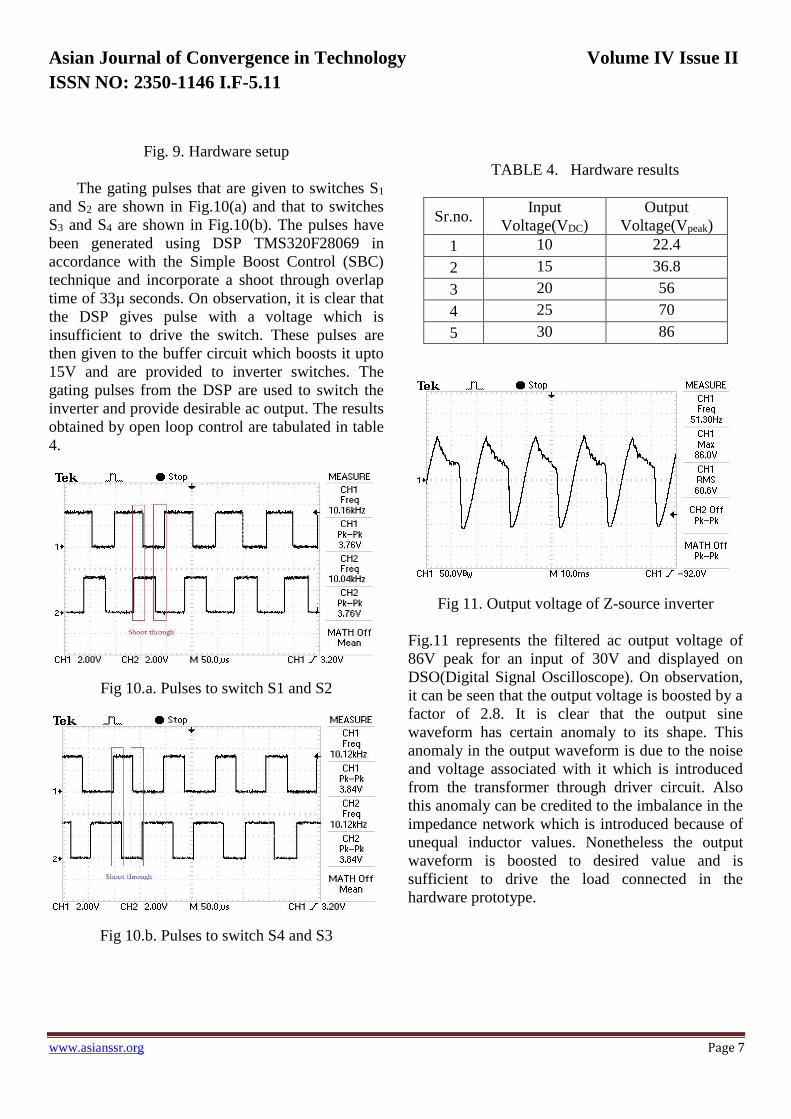
Fig.7. Hardware prototype of auxiliary supply and
buffer circuit
Fig.7 shows the hardware implementation for
auxiliary power supply and driver circuit board. The
stepped down ac supply fed through the step down
transformer of rating 230V/18V. The ac voltage is
then converted into dc by use of diode bridge
rectifier. Further arrangements can then be seen into
the schematic diagram. Driver circuit is connected
to the auxiliary power supply thus providing gate
pulses to IGBT switches.
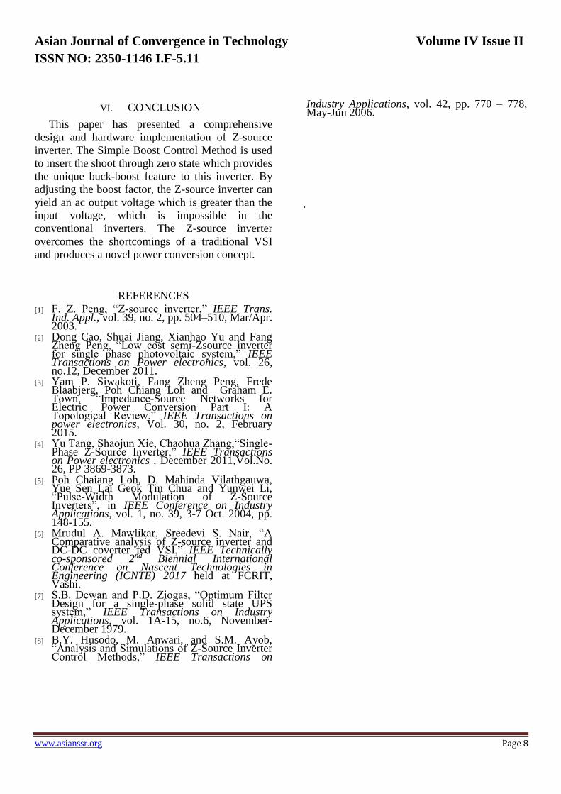
Fig.8. Hardware prototype of Z-source inverter
The hardware implementation of Z-source
inverter is shown in Fig.8. The hardware setup is
shown in Fig.9. Four IGBTs with their heat sink are
mounted in the circuit. A fuse of 4A is incorporated
in series to the input of the circuit which provides
over current protection to the circuit. The switch
voltage rating is taken two to three times that of the
dc link voltage of 213V according to “(10)”. The
current rating is taken more than ten times that of
the output current of 1.69A. By taking into
consideration the above mentioned constraints,
availability and cost, IGBT FGH60N60UFD is
selected for hardware implementation.
Asian Journal of Convergence in Technology Volume IV Issue II
ISSN NO: 2350-1146 I.F-5.11
www.asianssr.org Page 7
Fig. 9. Hardware setup
The gating pulses that are given to switches S1
and S2 are shown in Fig.10(a) and that to switches
S3 and S4 are shown in Fig.10(b). The pulses have
been generated using DSP TMS320F28069 in
accordance with the Simple Boost Control (SBC)
technique and incorporate a shoot through overlap
time of 33µ seconds. On observation, it is clear that
the DSP gives pulse with a voltage which is
insufficient to drive the switch. These pulses are
then given to the buffer circuit which boosts it upto
15V and are provided to inverter switches. The
gating pulses from the DSP are used to switch the
inverter and provide desirable ac output. The results
obtained by open loop control are tabulated in table
4.
Fig 10.a. Pulses to switch S1 and S2
Fig 10.b. Pulses to switch S4 and S3
TABLE 4. Hardware results
Sr.no. Input
Voltage(VDC)
Output
Voltage(Vpeak)
1 10 22.4
2 15 36.8
3 20 56
4 25 70
5 30 86
Fig 11. Output voltage of Z-source inverter
Fig.11 represents the filtered ac output voltage of
86V peak for an input of 30V and displayed on
DSO(Digital Signal Oscilloscope). On observation,
it can be seen that the output voltage is boosted by a
factor of 2.8. It is clear that the output sine
waveform has certain anomaly to its shape. This
anomaly in the output waveform is due to the noise
and voltage associated with it which is introduced
from the transformer through driver circuit. Also
this anomaly can be credited to the imbalance in the
impedance network which is introduced because of
unequal inductor values. Nonetheless the output
waveform is boosted to desired value and is
sufficient to drive the load connected in the
hardware prototype.
Asian Journal of Convergence in Technology Volume IV Issue II
ISSN NO: 2350-1146 I.F-5.11
www.asianssr.org Page 8
VI. CONCLUSION
This paper has presented a comprehensive
design and hardware implementation of Z-source
inverter. The Simple Boost Control Method is used
to insert the shoot through zero state which provides
the unique buck-boost feature to this inverter. By
adjusting the boost factor, the Z-source inverter can
yield an ac output voltage which is greater than the
input voltage, which is impossible in the
conventional inverters. The Z-source inverter
overcomes the shortcomings of a traditional VSI
and produces a novel power conversion concept.
REFERENCES
[1] F. Z. Peng, “Z-source inverter,” IEEE Trans. Ind. Appl., vol. 39, no. 2, pp. 504–510, Mar/Apr. 2003.
[2] Dong Cao, Shuai Jiang, Xianhao Yu and Fang Zheng Peng, “Low cost semi-Zsource inverter for single phase photovoltaic system,” IEEE Transactions on Power electronics, vol. 26, no.12, December 2011.
[3] Yam P. Siwakoti, Fang Zheng Peng, Frede Blaabjerg, Poh Chiang Loh and Graham E. Town, “Impedance-Source Networks for Electric Power Conversion Part I: A Topological Review,” IEEE Transactions on power electronics, Vol. 30, no. 2, February 2015.
[4] Yu Tang, Shaojun Xie, Chaohua Zhang,“Single-Phase Z-Source Inverter,” IEEE Transactions on Power electronics , December 2011,Vol.No. 26, PP 3869-3873.
[5] Poh Chaiang Loh, D. Mahinda Vilathgauwa, Yue Sen Lai Geok Tin Chua and Yunwei Li, “Pulse-Width Modulation of Z-Source Inverters”, in IEEE Conference on Industry Applications, vol. 1, no. 39, 3-7 Oct. 2004, pp. 148-155.
[6] Mrudul A. Mawlikar, Sreedevi S. Nair, “A Comparative analysis of Z-source inverter and DC-DC coverter fed VSI,” IEEE Technically co-sponsored 2nd Biennial International Conference on Nascent Technologies in Engineering (ICNTE) 2017 held at FCRIT, Vashi.
[7] S.B. Dewan and P.D. Ziogas, “Optimum Filter Design for a single-phase solid state UPS system,” IEEE Transactions on Industry Applications, vol. 1A-15, no.6, November-December 1979.
[8] B.Y. Husodo, M. Anwari, and S.M. Ayob, “Analysis and Simulations of Z-Source Inverter Control Methods,” IEEE Transactions on
Industry Applications, vol. 42, pp. 770 – 778, May-Jun 2006.
.
Recommended