Nanjing extension of Microelectronics Co., Ltd. TP5100
Nanjing extension of Microelectronics Co., Ltd.
NanJing NanJing NanJing NanJing Top Top Top Top PowerPower Power PowerASICASIC ASIC ASIC Corp.Corp. Corp. Corp.
Data Sheet
DATASHEET
TP5100 UTP5100 U
2A-switch buck 8.4V / 4.2V rechargeable lithium battery
Chip

Nanjing extension of Microelectronics Co., Ltd. TP5100
1111
Outline
TP5100 is a step-down switching double 8.4V / 4.2V single lithium battery charge management chip. QFN16 ultra small package with its simple
external circuit, so that the large current charging management application TP5100 ideal for portable devices. Meanwhile, TP5100 built-in input overcurrent,
undervoltage protection, over temperature protection, short circuit protection, battery temperature monitoring, reverse battery protection.
TP5100 having a wide input voltage 5V-18V, the battery trickle charging into pre-charge, constant current, constant-voltage three phase, pre-charge
current trickle charge current is adjusted through an external resistor, the maximum charging current of 2A. TP5100 using frequency of 400kHz switching
mode makes it possible to use a smaller peripheral devices, and still maintain a smaller amount of heat in the large current charging. TP5100 built-in power
of the PMOSFET, anti-intrusion circuit, there is no need peripheral anti-intrusion protection Schottky diode.
characteristic
■ Dual / single 8.4V / 4.2V rechargeable lithium battery
■ Built-in power MOSFET, a switching mode of operation, less
heating device, a simple peripheral
■ Programmable charge current, 0.1A - 2A
■ Programmable precharge current, 10% - 100%
■ No external Schottky diode anti-intrusion
■ Wide operating voltage, maximum reach 18V
■ Red and green LED indicates the state of charge
■ Chip temperature protection, overcurrent, undervoltage protection
■ Battery temperature protection, reverse battery shutdown, short circuit protection
■ Switching frequency of 400KHz, and more available inductance 20uH
■ PWR_ON- power, battery-powered switching control
■ Charging voltage control accuracy of less than 1%
■ Trickle, constant current, constant voltage charging three sections, a battery protection
■ QFN16 4mm * 4mm using ultra small package
Absolute Maximum Ratings
■ Static input supply voltage (VIN): 20V
■ BAT : -8.4V ~ 20VBAT : -8.4V ~ 20V
■ BAT Short circuit duration: ContinuousBAT Short circuit duration: Continuous
■ Maximum junction temperature: 120 ℃
■ Working temperature range: -40 ℃ ~ 85 ℃
■ Storage Temperature Range: -65 ℃ ~ 125 ℃
■ Lead Temperature (welding time of 10 seconds): 260 ℃
application
■ Portable equipment, various chargers
■ Smart phone, PDA, mobile cellular phone
■ MP4, MP5 players, tablet computers
■ HM
■ electrical tools
■ Interphone
typical application
FIG 2 TP5100 lithium ion battery is 8.4V 1.5A double charge (precharge 150MA) Application schematic

Nanjing extension of Microelectronics Co., Ltd. TP5100
2222
FIG 1 TP5100 is a single 4.2V rechargeable lithium ion battery 1.5A (prefilled 150MA) Application schematic
Ordering Information Package ////
16 Pin 4mm * 4mmQFN16 A top view of the package16 Pin 4mm * 4mmQFN16 A top view of the package16 Pin 4mm * 4mmQFN16 A top view of the package16 Pin 4mm * 4mmQFN16 A top view of the package
(Fin ground)
Orders models
TP5100-QFN16
Device Marking
TP5100
Physical picture

Nanjing extension of Microelectronics Co., Ltd. TP5100
3333
TP TP TPTP5100510051005100 Functional 510051005100 Functional block diagram
Map 3 TP5100 Functional Block DiagramMap 3 TP5100 Functional Block DiagramMap 3 TP5100 Functional Block Diagram

Nanjing extension of Microelectronics Co., Ltd. TP5100
4444
Electrical characteristics
Table 1 TP5100 electric characteristics can parameter
Where ● denotes specifications which apply 8.4V, 4.2V mode, otherwise specifications 8.4V, T R A R = 25 ℃, VIN = 12V, except where indicated otherwise.Where ● denotes specifications which apply 8.4V, 4.2V mode, otherwise specifications 8.4V, T R A R = 25 ℃, VIN = 12V, except where indicated otherwise.Where ● denotes specifications which apply 8.4V, 4.2V mode, otherwise specifications 8.4V, T R A R = 25 ℃, VIN = 12V, except where indicated otherwise.Where ● denotes specifications which apply 8.4V, 4.2V mode, otherwise specifications 8.4V, T R A R = 25 ℃, VIN = 12V, except where indicated otherwise.Where ● denotes specifications which apply 8.4V, 4.2V mode, otherwise specifications 8.4V, T R A R = 25 ℃, VIN = 12V, except where indicated otherwise.
symbol parameter condition Min Typ Max Units
VIN Input supply voltage ● 4.5 12 18 V
I R CC I R CC I R CC Input supply current
No battery mode, R R S R = 0.1 Ω standby No battery mode, R R S R = 0.1 Ω standby No battery mode, R R S R = 0.1 Ω standby No battery mode, R R S R = 0.1 Ω standby No battery mode, R R S R = 0.1 Ω standby No battery mode, R R S R = 0.1 Ω standby No battery mode, R R S R = 0.1 Ω standby
mode (charge termination) Stop
mode ( CS = GND ,mode ( CS = GND ,mode ( CS = GND ,
V R in R < V R BAT R ,or V R in R < V R UV R )V R in R < V R BAT R ,or V R in R < V R UV R )V R in R < V R BAT R ,or V R in R < V R UV R )V R in R < V R BAT R ,or V R in R < V R UV R )V R in R < V R BAT R ,or V R in R < V R UV R )V R in R < V R BAT R ,or V R in R < V R UV R )V R in R < V R BAT R ,or V R in R < V R UV R )V R in R < V R BAT R ,or V R in R < V R UV R )V R in R < V R BAT R ,or V R in R < V R UV R )V R in R < V R BAT R ,or V R in R < V R UV R )V R in R < V R BAT R ,or V R in R < V R UV R )V R in R < V R BAT R ,or V R in R < V R UV R )V R in R < V R BAT R ,or V R in R < V R UV R )V R in R < V R BAT R ,or V R in R < V R UV R )V R in R < V R BAT R ,or V R in R < V R UV R )V R in R < V R BAT R ,or V R in R < V R UV R )V R in R < V R BAT R ,or V R in R < V R UV R )V R in R < V R BAT R ,or V R in R < V R UV R )
●
●
●
150 180 μ Aμ A
μ Aμ A
μ Aμ A
V R FLOAL V R FLOAL V R FLOAL Charge cutoff voltage
4.2V Lithium Ion Battery 4.2V Lithium Ion Battery 4.158 4.2 4.242 V
8.4V Lithium Ion Battery 8.4V Lithium Ion Battery 8.316 8.4 8.484 V
I R BATI R BATI R BAT
BAT Pin Current:BAT Pin Current:
( Current mode test conditions( Current mode test conditions
CS = VREG Battery = 7.5V)CS = VREG Battery = 7.5V)CS = VREG Battery = 7.5V)
R R S = 0.1 Ω, constant current modeR R S = 0.1 Ω, constant current modeR R S = 0.1 Ω, constant current modeR R S = 0.1 Ω, constant current modeR R S = 0.1 Ω, constant current mode
R R S R = 0.067 [Omega], the constant current R R S R = 0.067 [Omega], the constant current R R S R = 0.067 [Omega], the constant current R R S R = 0.067 [Omega], the constant current R R S R = 0.067 [Omega], the constant current R R S R = 0.067 [Omega], the constant current
mode, a standby mode, V R BAT R = 8.4V VIN mode, a standby mode, V R BAT R = 8.4V VIN mode, a standby mode, V R BAT R = 8.4V VIN mode, a standby mode, V R BAT R = 8.4V VIN mode, a standby mode, V R BAT R = 8.4V VIN mode, a standby mode, V R BAT R = 8.4V VIN
= 0V , V R BAT R = 8.4V= 0V , V R BAT R = 8.4V= 0V , V R BAT R = 8.4V= 0V , V R BAT R = 8.4V= 0V , V R BAT R = 8.4V= 0V , V R BAT R = 8.4V= 0V , V R BAT R = 8.4V
●
●
●
●
950 1000
1500
-1
-1
1100
-1
-1
mA
mA
uA
uA
I R TRIKLI R TRIKLI R TRIKL
Trickle pre-charge current
RTRICK Pin to groundRTRICK Pin to ground
1.2V <V R BAT R < V R TRIKL R ,1.2V <V R BAT R < V R TRIKL R ,1.2V <V R BAT R < V R TRIKL R ,1.2V <V R BAT R < V R TRIKL R ,1.2V <V R BAT R < V R TRIKL R ,1.2V <V R BAT R < V R TRIKL R ,1.2V <V R BAT R < V R TRIKL R ,1.2V <V R BAT R < V R TRIKL R ,1.2V <V R BAT R < V R TRIKL R ,
R R S R = 0.067R R S R = 0.067R R S R = 0.067R R S R = 0.067R R S R = 0.067
●
●
80 100 120 mA
F The oscillation frequency ● 350 400 500 KHz
D MAX D MAX The maximum duty cycle ● 100%
D MIN D MIN The minimum duty cycle ● 0%
V R TRIKLV R TRIKLV R TRIKL
Trickle charge threshold voltage ( 8.4V ) Trickle charge threshold voltage ( 4.2V ) R R S = 0.067 Ω,Trickle charge threshold voltage ( 8.4V ) Trickle charge threshold voltage ( 4.2V ) R R S = 0.067 Ω,Trickle charge threshold voltage ( 8.4V ) Trickle charge threshold voltage ( 4.2V ) R R S = 0.067 Ω,Trickle charge threshold voltage ( 8.4V ) Trickle charge threshold voltage ( 4.2V ) R R S = 0.067 Ω,Trickle charge threshold voltage ( 8.4V ) Trickle charge threshold voltage ( 4.2V ) R R S = 0.067 Ω,Trickle charge threshold voltage ( 8.4V ) Trickle charge threshold voltage ( 4.2V ) R R S = 0.067 Ω,Trickle charge threshold voltage ( 8.4V ) Trickle charge threshold voltage ( 4.2V ) R R S = 0.067 Ω,Trickle charge threshold voltage ( 8.4V ) Trickle charge threshold voltage ( 4.2V ) R R S = 0.067 Ω,Trickle charge threshold voltage ( 8.4V ) Trickle charge threshold voltage ( 4.2V ) R R S = 0.067 Ω,Trickle charge threshold voltage ( 8.4V ) Trickle charge threshold voltage ( 4.2V ) R R S = 0.067 Ω,
V R BAT R rise V R BAT R rise V R BAT R rise V R BAT R rise V R BAT R rise
5.6
2.8
5.8
2.9
6.0
3.0
V
V R TRHYS V R TRHYS V R TRHYS Trickle charge voltage hysteresis R R S = 0.067 Ω R R S = 0.067 Ω R R S = 0.067 Ω R R S = 0.067 Ω R R S = 0.067 Ω 60 80 100 mV
V R UV V R UV V R UV V R IN R Undervoltage lockout threshold V R IN R Undervoltage lockout threshold V R IN R Undervoltage lockout threshold V R IN R Undervoltage lockout threshold V R IN R Undervoltage lockout threshold From V R IN R Low to High From V R IN R Low to High From V R IN R Low to High From V R IN R Low to High From V R IN R Low to High From V R IN R Low to High ● 3.5 3.6 3.8 V
V R UVHYS V R UVHYS V R UVHYS V R IN R Undervoltage lockout hysteresis V R IN R Undervoltage lockout hysteresis V R IN R Undervoltage lockout hysteresis V R IN R Undervoltage lockout hysteresis V R IN R Undervoltage lockout hysteresis ● 150 200 300 mV
V R ASD V R ASD V R ASD V R IN R- V R BAT R Lockout threshold voltage V R IN R- V R BAT R Lockout threshold voltage V R IN R- V R BAT R Lockout threshold voltage V R IN R- V R BAT R Lockout threshold voltage V R IN R- V R BAT R Lockout threshold voltage V R IN R- V R BAT R Lockout threshold voltage V R IN R- V R BAT R Lockout threshold voltage V R IN R- V R BAT R Lockout threshold voltage V R IN R- V R BAT R Lockout threshold voltage
V R IN R From low to highV R IN R From low to highV R IN R From low to highV R IN R From low to highV R IN R From low to high
V R IN R High to LowV R IN R High to LowV R IN R High to LowV R IN R High to LowV R IN R High to Low
60 100 140 mV
mV
I R TERM I R TERM I R TERM C / 10 Termination current threshold C / 10 Termination current threshold R R S = 0.067 Ω R R S = 0.067 Ω R R S = 0.067 Ω R R S = 0.067 Ω R R S = 0.067 Ω ● 80 100 120 mA
CHRG
V Low voltage output pin
CHRG
I = 5mA ● 0.3 0.6 V
STDBY
V Pin output low
STDBY
I = 5mA ● 0.3 0.6 V
V R TEMP-H V R TEMP-H V R TEMP-H TEMP Pin high voltage shutdown TEMP Pin high voltage shutdown
● > 80 82
V R TEMP-L V R TEMP-L V R TEMP-L TEMP Pin low-end voltage shutdown TEMP Pin low-end voltage shutdown
● 43 <45 % * VREG
Δ V R RECHRG Δ V R RECHRG Δ V R RECHRG Δ V R RECHRG Threshold voltage of the rechargeable battery V R FLOAT R- V R RECHRG V R FLOAT R- V R RECHRG V R FLOAT R- V R RECHRG V R FLOAT R- V R RECHRG V R FLOAT R- V R RECHRG V R FLOAT R- V R RECHRG V R FLOAT R- V R RECHRG ● 80 150 200 mV
T R LIM T R LIM T R LIM Chip temperature protection 110 ℃
R R ON R R ON R R ON power FET "On" resistance power FET "On" resistance power FET "On" resistance 170 m Ωm Ω
t R ss t R ss t R ss Soft start time I R BAT R = 0 to I R BAT R = 0.1V / Rs I R BAT R = 0 to I R BAT R = 0.1V / Rs I R BAT R = 0 to I R BAT R = 0.1V / Rs I R BAT R = 0 to I R BAT R = 0.1V / Rs I R BAT R = 0 to I R BAT R = 0.1V / Rs I R BAT R = 0 to I R BAT R = 0.1V / Rs I R BAT R = 0 to I R BAT R = 0.1V / Rs I R BAT R = 0 to I R BAT R = 0.1V / Rs I R BAT R = 0 to I R BAT R = 0.1V / Rs I R BAT R = 0 to I R BAT R = 0.1V / Rs I R BAT R = 0 to I R BAT R = 0.1V / Rs 20 u Su S
t R RECHARGE t R RECHARGE t R RECHARGE Filter Time recharge V R BAT R High to Low V R BAT R High to Low V R BAT R High to Low V R BAT R High to Low V R BAT R High to Low 0.8 1.8 4 mS
t R TERM t R TERM t R TERM Termination Comparator Filter Time I R BAT R Drops C R / 10 the following I R BAT R Drops C R / 10 the following I R BAT R Drops C R / 10 the following I R BAT R Drops C R / 10 the following I R BAT R Drops C R / 10 the following I R BAT R Drops C R / 10 the following I R BAT R Drops C R / 10 the following I R BAT R Drops C R / 10 the following I R BAT R Drops C R / 10 the following 0.8 1.8 4 mS
530
50
1450
0
0
1600
120
120
120
140
140
140
% * VREG

Nanjing extension of Microelectronics Co., Ltd. TP5100
5555
Typical performance indicators ( CSTypical performance indicators ( CSCS CS CS Set as 8.4CS CS CS Set as 8.4CS CS CS Set as 8.48.48.48.4VVVV Lithium battery charging mode)8.4VVVV Lithium battery charging mode)
The relationship between cut off voltage and the supply voltage and the ambient temperature relation of the charging voltage and the battery current-voltage relationship
Efficiency versus supply voltage

Nanjing extension of Microelectronics Co., Ltd. TP5100
6666
Pin Function
VIN VIN VIN VIN (Pins 1111 , 4444 , 5555VIN VIN VIN VIN (Pins 1111 , 4444 , 5555VIN VIN VIN VIN (Pins 1111 , 4444 , 5555VIN VIN VIN VIN (Pins 1111 , 4444 , 5555VIN VIN VIN VIN (Pins 1111 , 4444 , 5555VIN VIN VIN VIN (Pins 1111 , 4444 , 5555VIN VIN VIN VIN (Pins 1111 , 4444 , 5555, 16, 16 161 616 ): Input voltage at the 161 616 ): Input voltage at the positive input
end . This voltage is the power supply pin of the internal circuit,end . This voltage is the power supply pin of the internal circuit,
VIN Changes in scope 5V to 18V Between, and through a 10uF with 0.1uFVIN Changes in scope 5V to 18V Between, and through a 10uF with 0.1uFVIN Changes in scope 5V to 18V Between, and through a 10uF with 0.1uFVIN Changes in scope 5V to 18V Between, and through a 10uF with 0.1uFVIN Changes in scope 5V to 18V Between, and through a 10uF with 0.1uFVIN Changes in scope 5V to 18V Between, and through a 10uF with 0.1uFVIN Changes in scope 5V to 18V Between, and through a 10uF with 0.1uFVIN Changes in scope 5V to 18V Between, and through a 10uF with 0.1uFVIN Changes in scope 5V to 18V Between, and through a 10uF with 0.1uF
Bypass capacitor. when VIN withBypass capacitor. when VIN withBypass capacitor. when VIN with
V R BAT R Pressure lower than 30mv Time, TP5100 Enter shutdown mode, V R BAT R Pressure lower than 30mv Time, TP5100 Enter shutdown mode, V R BAT R Pressure lower than 30mv Time, TP5100 Enter shutdown mode, V R BAT R Pressure lower than 30mv Time, TP5100 Enter shutdown mode, V R BAT R Pressure lower than 30mv Time, TP5100 Enter shutdown mode, V R BAT R Pressure lower than 30mv Time, TP5100 Enter shutdown mode, V R BAT R Pressure lower than 30mv Time, TP5100 Enter shutdown mode, V R BAT R Pressure lower than 30mv Time, TP5100 Enter shutdown mode, V R BAT R Pressure lower than 30mv Time, TP5100 Enter shutdown mode,
reducing the I R BAT R Drops 1 μ A .reducing the I R BAT R Drops 1 μ A .reducing the I R BAT R Drops 1 μ A .reducing the I R BAT R Drops 1 μ A .reducing the I R BAT R Drops 1 μ A .reducing the I R BAT R Drops 1 μ A .reducing the I R BAT R Drops 1 μ A .reducing the I R BAT R Drops 1 μ A .reducing the I R BAT R Drops 1 μ A .reducing the I R BAT R Drops 1 μ A .
LX LX LX LX (Pins 2222 , 3333 ): Built-in power drain of PMOSFET LX LX LX LX (Pins 2222 , 3333 ): Built-in power drain of PMOSFET LX LX LX LX (Pins 2222 , 3333 ): Built-in power drain of PMOSFET LX LX LX LX (Pins 2222 , 3333 ): Built-in power drain of PMOSFET LX LX LX LX (Pins 2222 , 3333 ): Built-in power drain of PMOSFET LX LX LX LX (Pins 2222 , 3333 ): Built-in power drain of PMOSFET
connection point . LX is TP5100 current output terminal of the external connection point . LX is TP5100 current output terminal of the external
inductor is connected to a battery charging current input terminal.
PWR_ON- PWR_ON- PWR_ON- PWR_ON - (((( Pin 6)(((( Pin 6)(((( Pin 6) 6)6)6) : Power switching control pin.6) : Power switching control pin.
When the chip is connected to the power supply, PWR_ON- Internal switch When the chip is connected to the power supply, PWR_ON- Internal switch When the chip is connected to the power supply, PWR_ON- Internal switch
is pulled low, the drive PMOS Conducting, when the chip is not connected is pulled low, the drive PMOS Conducting, when the chip is not connected is pulled low, the drive PMOS Conducting, when the chip is not connected
to the power supply, PWR_ON- Internal switch is pulled to a high levelto the power supply, PWR_ON- Internal switch is pulled to a high levelto the power supply, PWR_ON- Internal switch is pulled to a high level
BAT End of the battery voltage, the driving PMOS Shutdown. This pin can BAT End of the battery voltage, the driving PMOS Shutdown. This pin can BAT End of the battery voltage, the driving PMOS Shutdown. This pin can BAT End of the battery voltage, the driving PMOS Shutdown. This pin can
be used to switch the power supply, the power source can also be used to
establish the detection is normal.
GND GND GND GND (Pins 7777 ): Power GND GND GND GND (Pins 7777 ): Power GND GND GND GND (Pins 7777 ): Power GND GND GND GND (Pins 7777 ): Power Ground .Ground .
VS VS VS VS (Pins 8888 ): Positive input of the output current detection .VS VS VS VS (Pins 8888 ): Positive input of the output current detection .VS VS VS VS (Pins 8888 ): Positive input of the output current detection .VS VS VS VS (Pins 8888 ): Positive input of the output current detection .VS VS VS VS (Pins 8888 ): Positive input of the output current detection .
BAT BAT BAT BAT (Pins 9999 ): Battery voltage detection terminal . BAT BAT BAT BAT (Pins 9999 ): Battery voltage detection terminal . BAT BAT BAT BAT (Pins 9999 ): Battery voltage detection terminal . BAT BAT BAT BAT (Pins 9999 ): Battery voltage detection terminal . BAT BAT BAT BAT (Pins 9999 ): Battery voltage detection terminal .
The positive terminal of the battery is connected to this pin.
VREG VREG VREG VREG (Pins 10VREG (Pins 10VREG (Pins 10 101 010 ): Internal power supply . VREG is a101 010 ): Internal power supply . VREG is a101 010 ): Internal power supply . VREG is a
An internal power supply, it is an external bypass capacitor 0.1uF to
ground, the maximum possible drive 5mA.
TS TS TS TS (Pins TS TS TS TS (Pins 11 111 111 ): Battery temperature detection input 111 111 ): Battery temperature detection input terminal . willterminal . will
TS Pin to battery NTC (Negative temperature coefficient thermistor) sensor TS Pin to battery NTC (Negative temperature coefficient thermistor) sensor TS Pin to battery NTC (Negative temperature coefficient thermistor) sensor TS Pin to battery NTC (Negative temperature coefficient thermistor) sensor
output. in case TS Less than the voltage at pin VREG of 45% Or greater than output. in case TS Less than the voltage at pin VREG of 45% Or greater than output. in case TS Less than the voltage at pin VREG of 45% Or greater than output. in case TS Less than the voltage at pin VREG of 45% Or greater than output. in case TS Less than the voltage at pin VREG of 45% Or greater than output. in case TS Less than the voltage at pin VREG of 45% Or greater than output. in case TS Less than the voltage at pin VREG of 45% Or greater than
VREG Voltage 80% It means that the battery temperature is too low or too VREG Voltage 80% It means that the battery temperature is too low or too VREG Voltage 80% It means that the battery temperature is too low or too VREG Voltage 80% It means that the battery temperature is too low or too
high, the charging is suspended. in case TS Direct access GND Battery high, the charging is suspended. in case TS Direct access GND Battery high, the charging is suspended. in case TS Direct access GND Battery high, the charging is suspended. in case TS Direct access GND Battery high, the charging is suspended. in case TS Direct access GND Battery
temperature detection function is canceled, another charging function
properly.
RTRICK RTRICK RTRICK RTRICK (Pins 12RTRICK RTRICK (Pins 12RTRICK RTRICK (Pins 12121 212 ): Trickle precharge current set 121 212 ): Trickle precharge current set terminal .terminal .
will RTRICK Pin to ground to the pre-charge current 10%will RTRICK Pin to ground to the pre-charge current 10%will RTRICK Pin to ground to the pre-charge current 10%will RTRICK Pin to ground to the pre-charge current 10%
Setting a constant current, the precharge current may be provided by an
external resistor. in case RTRICK Floating the precharge current equals the external resistor. in case RTRICK Floating the precharge current equals the external resistor. in case RTRICK Floating the precharge current equals the
constant current.
CS CS CS CS (Pins CS CS CS CS (Pins 13 131 313 ): State lithium ion chip select input . CS131 313 ): State lithium ion chip select input . CS131 313 ): State lithium ion chip select input . CS131 313 ): State lithium ion chip select input . CS
Input terminal of the high level ( VREG ) Will TP5100 In the Input terminal of the high level ( VREG ) Will TP5100 In the Input terminal of the high level ( VREG ) Will TP5100 In the Input terminal of the high level ( VREG ) Will TP5100 In the Input terminal of the high level ( VREG ) Will TP5100 In the
lithium-ion battery 8.4V Off-state voltage. CS The vacant end TP5100lithium-ion battery 8.4V Off-state voltage. CS The vacant end TP5100lithium-ion battery 8.4V Off-state voltage. CS The vacant end TP5100lithium-ion battery 8.4V Off-state voltage. CS The vacant end TP5100lithium-ion battery 8.4V Off-state voltage. CS The vacant end TP5100lithium-ion battery 8.4V Off-state voltage. CS The vacant end TP5100
In the lithium ion battery 4.2V Off-state voltage. Low input level so TP5100In the lithium ion battery 4.2V Off-state voltage. Low input level so TP5100In the lithium ion battery 4.2V Off-state voltage. Low input level so TP5100In the lithium ion battery 4.2V Off-state voltage. Low input level so TP5100
It is shutdown. CS End can be TTL or CMOS Level of the drive It is shutdown. CS End can be TTL or CMOS Level of the drive It is shutdown. CS End can be TTL or CMOS Level of the drive It is shutdown. CS End can be TTL or CMOS Level of the drive It is shutdown. CS End can be TTL or CMOS Level of the drive It is shutdown. CS End can be TTL or CMOS Level of the drive It is shutdown. CS End can be TTL or CMOS Level of the drive
control.
STDBY STDBY STDBY STDBY (Pins 14STDBY STDBY (Pins 14STDBY STDBY (Pins 14141 414 ): Green battery charge means is 141 414 ): Green battery charge means is completed
Shows an end . When the battery is fully charged STDBY Internal switch Shows an end . When the battery is fully charged STDBY Internal switch Shows an end . When the battery is fully charged STDBY Internal switch Shows an end . When the battery is fully charged STDBY Internal switch
is pulled low to indicate the completion of charging. In addition,
STDBY The pin is in high impedance state.STDBY The pin is in high impedance state.
CHRG CHRG CHRG CHRG (Pins 15CHRG CHRG (Pins 15CHRG CHRG (Pins 15151 515 ): Red charging status indicator151 515 ): Red charging status indicator
end . When the battery is being charged, CHRG Internal switch pin is end . When the battery is being charged, CHRG Internal switch pin is end . When the battery is being charged, CHRG Internal switch pin is end . When the battery is being charged, CHRG Internal switch pin is
pulled low, indicating the charging progress; otherwise CHRG Pin is pulled low, indicating the charging progress; otherwise CHRG Pin is pulled low, indicating the charging progress; otherwise CHRG Pin is
high impedance.
Nanjing extension of Microelectronics Co., Ltd. TP5100
7777
working principle
TP5100 is designed for double 8.4V / 4.2V single lithium ion
battery designed for switching high current charger IC, a power transistor
chip inside the battery using the trickle, constant current and constant
voltage charging. The charging current can be programmed with an
external resistor, the charging current up to the maximum duration. 2A,
does not require additional anti-intrusion diode. TP5100 comprising two
open-drain output state indication output terminal, the charging indicator
status CHRG And FULL status outputs STDBY . Chip internal power status CHRG And FULL status outputs STDBY . Chip internal power status CHRG And FULL status outputs STDBY . Chip internal power status CHRG And FULL status outputs STDBY . Chip internal power status CHRG And FULL status outputs STDBY . Chip internal power
management circuitry automatically reduces the charging current of the
chip junction temperature exceeds 145 deg.] C, this feature allows the user
to use the maximum power handling capability of the chip, do not worry
about damaging the chip or the chip overheating external components.
When the input voltage is greater than the threshold voltage and
the chip enable the chip enable input terminal HIGH (the VREG) or
floating, TP5100 start charging the battery, CHRG Output pin low to floating, TP5100 start charging the battery, CHRG Output pin low to floating, TP5100 start charging the battery, CHRG Output pin low to
indicate that charging is in progress. If the lithium ion battery voltage is
lower than double 5.8V (Single lithium cell voltage is lower than the electron lower than double 5.8V (Single lithium cell voltage is lower than the electron lower than double 5.8V (Single lithium cell voltage is lower than the electron
2.9V ), The battery trickle charger for pre-charging (pre-charge current 2.9V ), The battery trickle charger for pre-charging (pre-charge current
through the external adjustable resistance) with a small current. The
constant current VS Pin and VBAT Determining the resistance between the constant current VS Pin and VBAT Determining the resistance between the constant current VS Pin and VBAT Determining the resistance between the constant current VS Pin and VBAT Determining the resistance between the constant current VS Pin and VBAT Determining the resistance between the
pin. When the lithium ion battery voltage is close to double 8.4V (Single pin. When the lithium ion battery voltage is close to double 8.4V (Single pin. When the lithium ion battery voltage is close to double 8.4V (Single
lithium-ion batteries close 4.2V ), The charge cut-off voltage of about from 50mVlithium-ion batteries close 4.2V ), The charge cut-off voltage of about from 50mVlithium-ion batteries close 4.2V ), The charge cut-off voltage of about from 50mVlithium-ion batteries close 4.2V ), The charge cut-off voltage of about from 50mV
(Connection resistance to the internal resistance of the battery voltage
differs depending on the circuit), the charging current is gradually reduced,
TP5100 constant voltage charging mode. When the charge current is
reduced to the off current, the charging period ends, CHRG End a high reduced to the off current, the charging period ends, CHRG End a high reduced to the off current, the charging period ends, CHRG End a high
impedance state, STDBY The low potential side.impedance state, STDBY The low potential side.impedance state, STDBY The low potential side.
When the battery voltage falls below the recharge threshold
(lithium ion battery double 8.1V / A single lithium ion battery 4.05V ), The (lithium ion battery double 8.1V / A single lithium ion battery 4.05V ), The (lithium ion battery double 8.1V / A single lithium ion battery 4.05V ), The (lithium ion battery double 8.1V / A single lithium ion battery 4.05V ), The (lithium ion battery double 8.1V / A single lithium ion battery 4.05V ), The
charge cycle starts automatically. Inside the chip precision voltage
reference source, an error amplifier and the resistor divider network to
ensure that the battery terminal voltage cutoff accuracy + - 1% Or less, to ensure that the battery terminal voltage cutoff accuracy + - 1% Or less, to ensure that the battery terminal voltage cutoff accuracy + - 1% Or less, to
meet the requirements of a lithium ion rechargeable battery. When the
input voltage or input voltage down below the battery voltage, the charger
enters a low power shutdown mode, no external anti-intrusion diode chip
drain from the battery approaches 1uA .drain from the battery approaches 1uA .drain from the battery approaches 1uA .
Charge cutoff voltage selection
TP5100 with double / single lithium two charging
Select the cutoff voltage. when CS Connected to the high potential terminalSelect the cutoff voltage. when CS Connected to the high potential terminalSelect the cutoff voltage. when CS Connected to the high potential terminal
VREG When, for the 8.4V double standard lithium-ion battery, 8.4V VREG When, for the 8.4V double standard lithium-ion battery, 8.4V
cut-off voltage. When the vacant terminal CS, the battery charging
standard battery Li-Ion, cutoff voltage 4.2V. When CS Termination low GND standard battery Li-Ion, cutoff voltage 4.2V. When CS Termination low GND standard battery Li-Ion, cutoff voltage 4.2V. When CS Termination low GND standard battery Li-Ion, cutoff voltage 4.2V. When CS Termination low GND
, The charger stops charging.
TP5100 composite design of the CS terminal can be determined
by an external control TP5100 is in charging mode is switched to the stop
mode.
When the vacant terminal CS, expressed as TP5100 single
lithium-ion batteries.
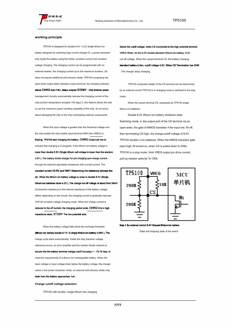
Double 8.4V lithium-ion battery shutdown state
Switching mode. 4, the output port of the CS terminal via an
open-drain, the gate of NMOS transistor if the input low, Nl off,
then terminating CS high, the charge-cutoff voltage of 8.4V,
TP5100 double Li-ion batteries. When the NMOS transistor gate
input high, Nl turned on, when CS is pulled down to GND,
TP5100 is a stop mode. 5mA VREG output pin drive current,
pull-up resistor optional 1k-100k.
Map 4 By external control 8.4V Shaped lithium-ion batteryMap 4 By external control 8.4V Shaped lithium-ion batteryMap 4 By external control 8.4V Shaped lithium-ion batteryMap 4 By external control 8.4V Shaped lithium-ion batteryMap 4 By external control 8.4V Shaped lithium-ion battery
State and stopping state of the switch
Nanjing extension of Microelectronics Co., Ltd. TP5100
8888
Charging current setting
Battery charging current I R BAT R, Is determined by the external current Battery charging current I R BAT R, Is determined by the external current Battery charging current I R BAT R, Is determined by the external current Battery charging current I R BAT R, Is determined by the external current Battery charging current I R BAT R, Is determined by the external current Battery charging current I R BAT R, Is determined by the external current
sense resistor Rs, Rs ratio adjust the threshold voltage Vs and the
constant charge current across the resistor is determined by the voltage
across the constant current condition Rs is 100mV.
FIG 5 is provided a battery charging current and the
charging current setting resistor is calculated using the following equation:
BAT S
IVR
10
= (Current units A Resistance per unit Ω )(Current units A Resistance per unit Ω )(Current units A Resistance per unit Ω )(Current units A Resistance per unit Ω )(Current units A Resistance per unit Ω )
For example:
To set the charging current 1A , Calculated into the formulaTo set the charging current 1A , Calculated into the formulaTo set the charging current 1A , Calculated into the formula
Rs = 0.1 ΩRs = 0.1 Ω
table 2 It gives some different settings corresponding to the current Rs Resistance, table 2 It gives some different settings corresponding to the current Rs Resistance, table 2 It gives some different settings corresponding to the current Rs Resistance, table 2 It gives some different settings corresponding to the current Rs Resistance, table 2 It gives some different settings corresponding to the current Rs Resistance,
to facilitate rapid design desired circuit. table 2 : Rs The charge current and to facilitate rapid design desired circuit. table 2 : Rs The charge current and to facilitate rapid design desired circuit. table 2 : Rs The charge current and to facilitate rapid design desired circuit. table 2 : Rs The charge current and to facilitate rapid design desired circuit. table 2 : Rs The charge current and
the corresponding
R S ( Ω)R S ( Ω)R S ( Ω) I R BAT I R BAT I R BAT R ( mA)R ( mA)
1 100
0.2 500
0.1 1000
0.067 1500
0.05 2000
Trickle precharge current is provided
If the battery voltage is below the precharge threshold voltage,
TP5100 A pre-charging operation starts charging the battery, TP5100 TP5100 A pre-charging operation starts charging the battery, TP5100 TP5100 A pre-charging operation starts charging the battery, TP5100
The pre-charge current by TRICKThe pre-charge current by TRICK
Port settings. A precharge current is employed in connection
TRICK Resistor connected between the pin and ground to set.TRICK Resistor connected between the pin and ground to set.
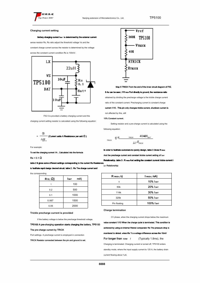
Map 6 TRICK From the end of the inner circuit diagram of FIG. Map 6 TRICK From the end of the inner circuit diagram of FIG. Map 6 TRICK From the end of the inner circuit diagram of FIG.
6 As can be seen, if R TRICK Port directly to ground, the resistance ratio 6 As can be seen, if R TRICK Port directly to ground, the resistance ratio 6 As can be seen, if R TRICK Port directly to ground, the resistance ratio 6 As can be seen, if R TRICK Port directly to ground, the resistance ratio 6 As can be seen, if R TRICK Port directly to ground, the resistance ratio
obtained by dividing the precharge voltage is the trickle charge current
ratio of the constant current. Precharging current is constant charge
current 1/10 . This pin only changes trickle current, shutdown current is current 1/10 . This pin only changes trickle current, shutdown current is current 1/10 . This pin only changes trickle current, shutdown current is
not affected by this, still
10% Constant current.10% Constant current.
Setting resistor and a pre-charge current is calculated using the
following equation:
TRICK BAT
BATTRICK
TRICK
II
kI
kI R
- -
=
40400
In order to facilitate customers to quickly design, table 3 Gives R TRICKIn order to facilitate customers to quickly design, table 3 Gives R TRICKIn order to facilitate customers to quickly design, table 3 Gives R TRICKIn order to facilitate customers to quickly design, table 3 Gives R TRICKIn order to facilitate customers to quickly design, table 3 Gives R TRICK
And the precharge current and constant trickle current setting of I BATAnd the precharge current and constant trickle current setting of I BATAnd the precharge current and constant trickle current setting of I BAT
Relationship. table 3 : R TRICK And setting the constant current trickle current IRelationship. table 3 : R TRICK And setting the constant current trickle current IRelationship. table 3 : R TRICK And setting the constant current trickle current IRelationship. table 3 : R TRICK And setting the constant current trickle current IRelationship. table 3 : R TRICK And setting the constant current trickle current IRelationship. table 3 : R TRICK And setting the constant current trickle current IRelationship. table 3 : R TRICK And setting the constant current trickle current I
BAT Relationship:BAT Relationship:
R TRICK ( k) R TRICK ( k) R TRICK ( k) I TRICK ( mA)I TRICK ( mA)I TRICK ( mA)
0 10% I BAT10% I BAT
50k 20% I BAT20% I BAT
114k 30% I BAT30% I BAT
320k 50% I BAT50% I BAT
Pin floating 100% I BAT100% I BAT
Charge termination
CV phase, when the charging current drops below the maximum
value constant 1/10 When the charge cycle is terminated. This condition is value constant 1/10 When the charge cycle is terminated. This condition is value constant 1/10 When the charge cycle is terminated. This condition is
achieved by using an internal filtered comparator Rs The pressure drop is achieved by using an internal filtered comparator Rs The pressure drop is achieved by using an internal filtered comparator Rs The pressure drop is
monitored to detect. when Rs To a voltage difference across the 10mVmonitored to detect. when Rs To a voltage difference across the 10mVmonitored to detect. when Rs To a voltage difference across the 10mVmonitored to detect. when Rs To a voltage difference across the 10mV
For longer than TERMFor longer than TERM t (Typically 1.8ms), the
Charging is terminated. Charging current is turned off, TP5100 enters
standby mode, where the input supply current to 120 A, the battery drain
current flowing about 1uA.

Nanjing extension of Microelectronics Co., Ltd. TP5100
9999
In standby mode, TP5100 of BAT Pin voltage is continuously In standby mode, TP5100 of BAT Pin voltage is continuously In standby mode, TP5100 of BAT Pin voltage is continuously
monitored. If the lithium ion battery double this voltage drops 8.25V (single
lithium battery voltage drops below
4.05V) recharging limit switches RECHRG4.05V) recharging limit switches RECHRGV Or less, the new
The charge cycle begins again and supplying current to the battery.
Charging status indicator
TP5100 Two open-drain status output terminal, CHRG with STDBY TP5100 Two open-drain status output terminal, CHRG with STDBY TP5100 Two open-drain status output terminal, CHRG with STDBY TP5100 Two open-drain status output terminal, CHRG with STDBY
. When the charger is in the charging state, CHRG It is pulled low, in . When the charger is in the charging state, CHRG It is pulled low, in . When the charger is in the charging state, CHRG It is pulled low, in
other states, CHRG In a high impedance state. When the outside other states, CHRG In a high impedance state. When the outside other states, CHRG In a high impedance state. When the outside
temperature of the battery is in a normal temperature range, CHRG withtemperature of the battery is in a normal temperature range, CHRG withtemperature of the battery is in a normal temperature range, CHRG with
STDBY Pins are high impedance. When no indication state, the pin STDBY Pins are high impedance. When no indication state, the pin
can not be connected to ground. Table 4: state of charge indicator
Green
STDBY
red light
CHRG
charging
Destroy bright Charging status
bright Destroy Battery is fully charged state
Destroy Destroy
Voltage, battery temperature is
too high, too low or non-fault
state battery Access (TS end
use)
Green light, red light flashes
T = 0.5-1S
BAT termination 10u capacitor,
no battery standby state (TS
ground)
Power, battery switching control
TP5100 integrated power, battery power supply switch control pin
PWR_ON-. When the input VIN, PWR_ON- output low, may be turned on
PMOS. When VIN is removed, PWR_ON- outputting the high potential
(battery voltage) can be closed PMOS.
Map 7 A schematic view of the control power supply switchMap 7 A schematic view of the control power supply switchMap 7 A schematic view of the control power supply switch
Battery over-temperature protection
In order to prevent the temperature is too high or too low battery
damage caused, TP5100 integrated internal battery temperature detecting
circuit. Battery temperature is detected by measuring the voltage pin TS
implemented, the voltage pin TS is an NTC thermistor in a battery and a
resistor divider network, as shown in FIG. TP5100 inside the TS pin chip
with two voltage thresholds LOWwith two voltage thresholds LOW
V with HIGHV with HIGHV with HIGH V Compared toV Compared to
Confirm that the battery temperature exceeds a normal range. Inside
the TP5100, LOWthe TP5100, LOW
V Is fixedV Is fixed
VREG×45% , HIGH, HIGH V Is fixed
VREG×80% . If the TS pin voltage
LOW TS VV <TS VV <
or
HIGH TS VV>TS VV>
, The battery
The temperature is too high or too low, the charging process is suspended;
if voltage pin TS TSif voltage pin TS TS
V in LOWV in LOWV in LOW V with HIGHV with HIGHV with HIGH V ItV It
Among the charge cycle continues. If the TS pin to ground, battery
temperature detection function can be disabled.
Example: room temperature 25 ℃ RNTC = 10k, set protection
temperature 60 ℃, at 60 ℃ RNTC = 3k, R = 3.6k the calculated time, the
NTC resistor-divider ratio of 45% VREG voltage, i.e., when the stop 60 ℃
TP5100 charge.
Map 8 NTC Connection diagramMap 8 NTC Connection diagramMap 8 NTC Connection diagram
Chip internal thermal limit
If the chip temperature attempts to rise to about 110 ℃
predetermined value or more, the heat inside a feedback loop to reduce
the charge current is set. This feature prevents overheating TP5100, and
allows the user increases the maximum for a given power handling
capability of the circuit board without risk of damaging the TP5100. In
ensuring the charger will automatically reduce the current in the worst case
conditions of the premise, according to a typical (but not the worst case)
the ambient temperature is set to the charging current.

Nanjing extension of Microelectronics Co., Ltd. TP5100
10,101,010
Limiting the short-circuit and an output
TP5100 integrates a variety of protection, the chip input limiting the
maximum peak current. 3A, to prevent chip damage due to excessive
current. When the output voltage below about 1.2V, the chip into
short-circuit protection mode, the chip input current limit is 10% of the
maximum peak current of about 450mA. Of different magnitude of the
current with the input voltage difference.
Automatic restart
Once the charge cycle is terminated, TP5100 immediately
takes time having a 1.8ms filter ( RECHARGEtakes time having a 1.8ms filter ( RECHARGE
t )of
Comparator continuously monitors the voltage on the BAT pin. When the
battery voltage falls below 90% of the battery capacity, the charging cycle
begins again. This ensures that the battery is maintained at (or near) a
fully charged state. In the recharge cycle, CHRG Output pin to re-enter a fully charged state. In the recharge cycle, CHRG Output pin to re-enter a fully charged state. In the recharge cycle, CHRG Output pin to re-enter a
strong pull-down state.
Map 9 A typical lithium-ion battery circulation state in FIG.Map 9 A typical lithium-ion battery circulation state in FIG.Map 9 A typical lithium-ion battery circulation state in FIG.
Undervoltage lockout
An internal undervoltage lockout circuit monitors the input voltage,
and Vin It rises above the undervoltage lockout threshold before the and Vin It rises above the undervoltage lockout threshold before the and Vin It rises above the undervoltage lockout threshold before the
charger in shutdown mode. UVLO Charger circuitry will remain in shutdown charger in shutdown mode. UVLO Charger circuitry will remain in shutdown charger in shutdown mode. UVLO Charger circuitry will remain in shutdown
mode, no discharge current of the battery. in case UVLO The comparator mode, no discharge current of the battery. in case UVLO The comparator mode, no discharge current of the battery. in case UVLO The comparator
transition occurs at VIN Raised higher than the battery voltage 50mV Before transition occurs at VIN Raised higher than the battery voltage 50mV Before transition occurs at VIN Raised higher than the battery voltage 50mV Before transition occurs at VIN Raised higher than the battery voltage 50mV Before transition occurs at VIN Raised higher than the battery voltage 50mV Before
charger will not exit the shutdown mode. So customers do not worry about
the battery level is vented when the input power shortage situation.
Input, output, terminal of the capacitor VS
You can use many types of capacitors, but requires high-quality
power capacitors. When the multilayer ceramic capacitor with particular
care must be taken, some types of ceramic capacitors having high EMI
characteristic values, therefore, under certain conditions (such as the
battery charger is connected to the power supply input and a work) may
produce a high voltage transient damaging the chip signal form, and
recommended 0.1uF capacitor 10uF X5R or X7R material or ceramic
capacitor, and the capacitance connected to a position close to the chip pin sure.
Thermal Considerations
although QFN16 The small form factor package, but its good heat although QFN16 The small form factor package, but its good heat although QFN16 The small form factor package, but its good heat
dissipation properties, but need PCB With the preferred version of the dissipation properties, but need PCB With the preferred version of the dissipation properties, but need PCB With the preferred version of the
design, it is preferably designed using a hot well PCBdesign, it is preferably designed using a hot well PCB
Plate layout to most significantly increase the charging current may be
used. For dissipate IC Cooling path of the generated heat from the chip to used. For dissipate IC Cooling path of the generated heat from the chip to used. For dissipate IC Cooling path of the generated heat from the chip to
the lead frame, by die and reaches the bottom of the fin PCB Board the lead frame, by die and reaches the bottom of the fin PCB Board the lead frame, by die and reaches the bottom of the fin PCB Board
copper. The footprint copper pads should be as wide, and extends
outwardly to a large copper area to spread the heat to the surroundings. It
recommended to pay more through holes inside or backside copper layer,
to improve the overall thermal performance of the charger. When
performing PCB Board layout design, other heat sources related to the performing PCB Board layout design, other heat sources related to the performing PCB Board layout design, other heat sources related to the
charger board also must be considered, because they will affect overall
temperature rise and the maximum charge current has been affected.
Inductor Selection
To ensure system stability, and constant current charging the
pre-charge phase, the system needs to ensure that operate in continuous
mode (CCM). The inductor current equation:
BAT
IN
BAT IN
VVVV FS LI × ••• • ••• •
-
× = Δ 1
among them Iamong them IΔ Is the inductor ripple, FS is the switching frequency, in orderΔ Is the inductor ripple, FS is the switching frequency, in order
Nanjing extension of Microelectronics Co., Ltd. TP5100
11,111,111
To ensure that the precharge and a constant current charging mode are in CCM,
IΔ Take pre-charge current value, that is 1/5 of the constant current Δ Take pre-charge current value, that is 1/5 of the constant current
charging, the inductance value can be calculated according to the input voltage requirements.
22uH inductance values and above (inductance bigger and more
stable), recommended 22uH. If the power source VIN set 5V, 4.2V using a
single lithium-ion battery charging mode, and sets the charging current of
500mA or more, may be employed 10uH inductance.
Inductor rated current greater than a charge current is chosen, the
smaller the internal resistance of power inductors.

Nanjing extension of Microelectronics Co., Ltd. TP5100
12,121,212
Package Description 4mm * 4mm 16 Pin QFN Package4mm * 4mm 16 Pin QFN Package4mm * 4mm 16 Pin QFN Package4mm * 4mm 16 Pin QFN Package
Only package reel / disc disc / cartridge box / boxes / box
QFN4 * 4 13 Inch 13 Inch 5000 1 8 40,000

Nanjing extension of Microelectronics Co., Ltd. TP5100
11,113,333
TP TP TPTP5100510051005100 Other 510051005100 Other application circuit
Map 10 TP5100 is 8.4V A lithium ion battery without the battery temperature protection 1.5A Application schematic chargingMap 10 TP5100 is 8.4V A lithium ion battery without the battery temperature protection 1.5A Application schematic chargingMap 10 TP5100 is 8.4V A lithium ion battery without the battery temperature protection 1.5A Application schematic chargingMap 10 TP5100 is 8.4V A lithium ion battery without the battery temperature protection 1.5A Application schematic chargingMap 10 TP5100 is 8.4V A lithium ion battery without the battery temperature protection 1.5A Application schematic chargingMap 10 TP5100 is 8.4V A lithium ion battery without the battery temperature protection 1.5A Application schematic chargingMap 10 TP5100 is 8.4V A lithium ion battery without the battery temperature protection 1.5A Application schematic charging
Map 11 TP5100 is 4.2V A lithium ion battery without the battery temperature constant-current protection 1.5A Application schematic chargingMap 11 TP5100 is 4.2V A lithium ion battery without the battery temperature constant-current protection 1.5A Application schematic chargingMap 11 TP5100 is 4.2V A lithium ion battery without the battery temperature constant-current protection 1.5A Application schematic chargingMap 11 TP5100 is 4.2V A lithium ion battery without the battery temperature constant-current protection 1.5A Application schematic chargingMap 11 TP5100 is 4.2V A lithium ion battery without the battery temperature constant-current protection 1.5A Application schematic chargingMap 11 TP5100 is 4.2V A lithium ion battery without the battery temperature constant-current protection 1.5A Application schematic chargingMap 11 TP5100 is 4.2V A lithium ion battery without the battery temperature constant-current protection 1.5A Application schematic charging
( CS , PWR_ON- Pin floating)( CS , PWR_ON- Pin floating)( CS , PWR_ON- Pin floating)( CS , PWR_ON- Pin floating)( CS , PWR_ON- Pin floating)

Nanjing extension of Microelectronics Co., Ltd. TP5100
11,114,444
TP5100 Precautions
1. The circuit chip capacitors should be as close as possible.
2. VS terminal VIN and the BAT terminal and the terminal using 10u electrolytic capacitor 0.1uF, X5R or X7R ceramic capacitor level.
3. Please choose the inductor current capability enough power inductors.
4. Selection Schottky diode voltage drop greater than or equal 2A small current capability of the Schottky diode.
5. For VIN and LX to be wider than the signal line common trace current loop.
6. Note that the capacitance of each node location of the grounding line, that the grounding point should be focused, well grounded.
7. chip large current should be considered a good heat sink and the bottom of the chip to the PCB, to ensure good heat dissipation.
Recommended