101 Innovation DriveSan Jose, CA 95134www.altera.com
MNL-01075-1.4
Reference Manual
Cyclone V E FPGA Development Board
Feedback Subscribe
Cyclone V E FPGA Development Board Reference Manual

© 2017 Altera Corporation. All rights reserved. ALTERA, ARRIA, CYCLONE, HARDCOPY, MAX, MEGACORE, NIOS, QUARTUS and STRATIX words and logosare trademarks of Altera Corporation and registered in the U.S. Patent and Trademark Office and in other countries. All other words and logos identified astrademarks or service marks are the property of their respective holders as described at www.altera.com/common/legal.html. Altera warrants performance of itssemiconductor products to current specifications in accordance with Altera's standard warranty, but reserves the right to make changes to any products andservices at any time without notice. Altera assumes no responsibility or liability arising out of the application or use of any information, product, or servicedescribed herein except as expressly agreed to in writing by Altera. Altera customers are advised to obtain the latest version of device specifications before relyingon any published information and before placing orders for products or services.
August 2017 Altera Corporation Cyclone V E FPGA Development BoardReference Manual
ISO 9001:2008 Registered
August 2017 Altera Corporation
Contents
Chapter 1. OverviewGeneral Description . . . . . . . . . . . . . . . . . . . . . . . . . . . . . . . . . . . . . . . . . . . . . . . . . . . . . . . . . . . . . . . . . . . . . 1–1Board Component Blocks . . . . . . . . . . . . . . . . . . . . . . . . . . . . . . . . . . . . . . . . . . . . . . . . . . . . . . . . . . . . . . . . . 1–2Development Board Block Diagram . . . . . . . . . . . . . . . . . . . . . . . . . . . . . . . . . . . . . . . . . . . . . . . . . . . . . . . . 1–4Handling the Board . . . . . . . . . . . . . . . . . . . . . . . . . . . . . . . . . . . . . . . . . . . . . . . . . . . . . . . . . . . . . . . . . . . . . . 1–4
Chapter 2. Board ComponentsBoard Overview . . . . . . . . . . . . . . . . . . . . . . . . . . . . . . . . . . . . . . . . . . . . . . . . . . . . . . . . . . . . . . . . . . . . . . . . . 2–2Featured Device: Cyclone V E FPGA . . . . . . . . . . . . . . . . . . . . . . . . . . . . . . . . . . . . . . . . . . . . . . . . . . . . . . . 2–4
I/O Resources . . . . . . . . . . . . . . . . . . . . . . . . . . . . . . . . . . . . . . . . . . . . . . . . . . . . . . . . . . . . . . . . . . . . . . . . 2–5MAX V CPLD 5M2210 System Controller . . . . . . . . . . . . . . . . . . . . . . . . . . . . . . . . . . . . . . . . . . . . . . . . . . . 2–5FPGA Configuration . . . . . . . . . . . . . . . . . . . . . . . . . . . . . . . . . . . . . . . . . . . . . . . . . . . . . . . . . . . . . . . . . . . . 2–10
FPGA Programming over Embedded USB-Blaster II . . . . . . . . . . . . . . . . . . . . . . . . . . . . . . . . . . . . . . 2–10FPGA Programming from Flash Memory . . . . . . . . . . . . . . . . . . . . . . . . . . . . . . . . . . . . . . . . . . . . . . . 2–13FPGA Programming over External USB-Blaster . . . . . . . . . . . . . . . . . . . . . . . . . . . . . . . . . . . . . . . . . . 2–14FPGA Programming using EPCQ . . . . . . . . . . . . . . . . . . . . . . . . . . . . . . . . . . . . . . . . . . . . . . . . . . . . . . 2–15
Status Elements . . . . . . . . . . . . . . . . . . . . . . . . . . . . . . . . . . . . . . . . . . . . . . . . . . . . . . . . . . . . . . . . . . . . . . . . 2–15Setup Elements . . . . . . . . . . . . . . . . . . . . . . . . . . . . . . . . . . . . . . . . . . . . . . . . . . . . . . . . . . . . . . . . . . . . . . . . 2–16
Board Settings DIP Switch . . . . . . . . . . . . . . . . . . . . . . . . . . . . . . . . . . . . . . . . . . . . . . . . . . . . . . . . . . . . . 2–17JTAG Chain Control DIP Switch . . . . . . . . . . . . . . . . . . . . . . . . . . . . . . . . . . . . . . . . . . . . . . . . . . . . . . . 2–17CPU Reset Push Button . . . . . . . . . . . . . . . . . . . . . . . . . . . . . . . . . . . . . . . . . . . . . . . . . . . . . . . . . . . . . . . 2–17MAX V Reset Push Button . . . . . . . . . . . . . . . . . . . . . . . . . . . . . . . . . . . . . . . . . . . . . . . . . . . . . . . . . . . . 2–18Program Configuration Push Button . . . . . . . . . . . . . . . . . . . . . . . . . . . . . . . . . . . . . . . . . . . . . . . . . . . . 2–18Program Select Push Button . . . . . . . . . . . . . . . . . . . . . . . . . . . . . . . . . . . . . . . . . . . . . . . . . . . . . . . . . . . 2–18
Clock Circuitry . . . . . . . . . . . . . . . . . . . . . . . . . . . . . . . . . . . . . . . . . . . . . . . . . . . . . . . . . . . . . . . . . . . . . . . . . 2–18On-Board Oscillators . . . . . . . . . . . . . . . . . . . . . . . . . . . . . . . . . . . . . . . . . . . . . . . . . . . . . . . . . . . . . . . . . 2–18Off-Board Clock Input/Output . . . . . . . . . . . . . . . . . . . . . . . . . . . . . . . . . . . . . . . . . . . . . . . . . . . . . . . . 2–20
General User Input/Output . . . . . . . . . . . . . . . . . . . . . . . . . . . . . . . . . . . . . . . . . . . . . . . . . . . . . . . . . . . . . 2–20User-Defined Push Buttons . . . . . . . . . . . . . . . . . . . . . . . . . . . . . . . . . . . . . . . . . . . . . . . . . . . . . . . . . . . . 2–20User-Defined DIP Switch . . . . . . . . . . . . . . . . . . . . . . . . . . . . . . . . . . . . . . . . . . . . . . . . . . . . . . . . . . . . . 2–21User-Defined LEDs . . . . . . . . . . . . . . . . . . . . . . . . . . . . . . . . . . . . . . . . . . . . . . . . . . . . . . . . . . . . . . . . . . . 2–21
General LEDs . . . . . . . . . . . . . . . . . . . . . . . . . . . . . . . . . . . . . . . . . . . . . . . . . . . . . . . . . . . . . . . . . . . . . 2–21HSMC LEDs . . . . . . . . . . . . . . . . . . . . . . . . . . . . . . . . . . . . . . . . . . . . . . . . . . . . . . . . . . . . . . . . . . . . . . 2–22
Character LCD . . . . . . . . . . . . . . . . . . . . . . . . . . . . . . . . . . . . . . . . . . . . . . . . . . . . . . . . . . . . . . . . . . . . . . 2–22Debug Header . . . . . . . . . . . . . . . . . . . . . . . . . . . . . . . . . . . . . . . . . . . . . . . . . . . . . . . . . . . . . . . . . . . . . . . 2–23
Components and Interfaces . . . . . . . . . . . . . . . . . . . . . . . . . . . . . . . . . . . . . . . . . . . . . . . . . . . . . . . . . . . . . . 2–2410/100/1000 Ethernet . . . . . . . . . . . . . . . . . . . . . . . . . . . . . . . . . . . . . . . . . . . . . . . . . . . . . . . . . . . . . . . . 2–24HSMC . . . . . . . . . . . . . . . . . . . . . . . . . . . . . . . . . . . . . . . . . . . . . . . . . . . . . . . . . . . . . . . . . . . . . . . . . . . . . . 2–27RS-232 Serial UART . . . . . . . . . . . . . . . . . . . . . . . . . . . . . . . . . . . . . . . . . . . . . . . . . . . . . . . . . . . . . . . . . . 2–30USB-UART . . . . . . . . . . . . . . . . . . . . . . . . . . . . . . . . . . . . . . . . . . . . . . . . . . . . . . . . . . . . . . . . . . . . . . . . . . 2–31
Memory . . . . . . . . . . . . . . . . . . . . . . . . . . . . . . . . . . . . . . . . . . . . . . . . . . . . . . . . . . . . . . . . . . . . . . . . . . . . . . . 2–32DDR3 SDRAM . . . . . . . . . . . . . . . . . . . . . . . . . . . . . . . . . . . . . . . . . . . . . . . . . . . . . . . . . . . . . . . . . . . . . . 2–32LPDDR2 SDRAM . . . . . . . . . . . . . . . . . . . . . . . . . . . . . . . . . . . . . . . . . . . . . . . . . . . . . . . . . . . . . . . . . . . . 2–35EEPROM . . . . . . . . . . . . . . . . . . . . . . . . . . . . . . . . . . . . . . . . . . . . . . . . . . . . . . . . . . . . . . . . . . . . . . . . . . . 2–37Synchronous SRAM . . . . . . . . . . . . . . . . . . . . . . . . . . . . . . . . . . . . . . . . . . . . . . . . . . . . . . . . . . . . . . . . . . 2–38Flash . . . . . . . . . . . . . . . . . . . . . . . . . . . . . . . . . . . . . . . . . . . . . . . . . . . . . . . . . . . . . . . . . . . . . . . . . . . . . . . 2–39
Power Supply . . . . . . . . . . . . . . . . . . . . . . . . . . . . . . . . . . . . . . . . . . . . . . . . . . . . . . . . . . . . . . . . . . . . . . . . . . 2–41Power Distribution System . . . . . . . . . . . . . . . . . . . . . . . . . . . . . . . . . . . . . . . . . . . . . . . . . . . . . . . . . . . . 2–42
Cyclone V E FPGA Development BoardReference Manual
iv ContentsContents
Power Measurement . . . . . . . . . . . . . . . . . . . . . . . . . . . . . . . . . . . . . . . . . . . . . . . . . . . . . . . . . . . . . . . . . 2–43
Chapter 3. Board Components ReferenceBoard Components . . . . . . . . . . . . . . . . . . . . . . . . . . . . . . . . . . . . . . . . . . . . . . . . . . . . . . . . . . . . . . . . . . . . . . 3–1Statement of China-RoHS Compliance . . . . . . . . . . . . . . . . . . . . . . . . . . . . . . . . . . . . . . . . . . . . . . . . . . . . . 3–2CE EMI Conformity Caution . . . . . . . . . . . . . . . . . . . . . . . . . . . . . . . . . . . . . . . . . . . . . . . . . . . . . . . . . . . . . . 3–2
Additional InformationBoard Revision History . . . . . . . . . . . . . . . . . . . . . . . . . . . . . . . . . . . . . . . . . . . . . . . . . . . . . . . . . . . . . . . Info–1Document Revision History . . . . . . . . . . . . . . . . . . . . . . . . . . . . . . . . . . . . . . . . . . . . . . . . . . . . . . . . . . . Info–1Typographic Conventions . . . . . . . . . . . . . . . . . . . . . . . . . . . . . . . . . . . . . . . . . . . . . . . . . . . . . . . . . . . . . Info–1
Cyclone V E FPGA Development Board August 2017 Altera CorporationReference Manual
August 2017 Altera Corporation
1. Overview
This document describes the hardware features of the Cyclone® V E FPGA development board, including the detailed pin-out and component reference information required to create custom FPGA designs that interface with all components of the board.
General DescriptionThe Cyclone V E FPGA development board provides a hardware platform for developing and prototyping low-power, high-performance, and logic-intensive designs using Altera’s Cyclone V E FPGA. The board provides a wide range of peripherals and memory interfaces to facilitate the development of Cyclone V E FPGA designs.
One high-speed mezzanine card (HSMC) connector is available to add additional functionality via a variety of HSMCs available from Altera® and various partners.
f To see a list of the latest HSMCs available or to download a copy of the HSMC specification, refer to the Development Board Daughtercards page of the Altera website.
Design advancements and innovations, such as partial reconfiguration, ensure that designs implemented in the Cyclone V E FPGAs operate faster, with lower power, and have a faster time to market than previous FPGA families.
f For more information on the following topics, refer to the respective documents:
■ Cyclone V device family, refer to the Cyclone V Device Handbook.
■ HSMC Specification, refer to the High Speed Mezzanine Card (HSMC) Specification.
Cyclone V E FPGA Development BoardReference Manual
1–2 Chapter 1: OverviewBoard Component Blocks
Board Component BlocksThe development board features the following major component blocks:
■ One Cyclone V E FPGA (5CEFA7F31I7N) in a 896-pin FineLine BGA (FBGA) package
■ 149,500 LEs
■ 56,480 adaptive logic modules (ALMs)
■ 6,860 Kbit (Kb) M10K and 836 Kb MLAB memory
■ Seven fractional phase locked loops (PLLs)
■ 312 18x18-bit multipliers
■ 480 general purpose input/output (GPIO)
■ 1.1-V core voltage
■ FPGA configuration circuitry
■ Active Serial (AS) x1 or AS x4 configuration (EPCQ256SI16N)
■ MAX® V CPLD (5M2210ZF256I5N) in a 256-pin FBGA package as the System Controller
■ Flash fast passive parallel (FPP) configuration
■ MAX II CPLD (EPM240M100I5N) in a 100-pin FBGA package as part of the embedded USB-BlasterTM II for use with the Quartus® II Programmer
■ Clocking circuitry
■ Programmable clock generator for the FPGA reference clock input
■ 50-MHz single-ended oscillator for the FPGA and MAX V CPLD clock input
■ 100-MHz single-ended oscillator for the MAX V CPLD configuration clock input
■ SMA input (LVDS)
■ Memory
■ Two 256-Mbyte (MB) DDR3 SDRAM devices with a 16-bit data bus
■ One 18-Mbit (Mb) SSRAM
■ One 512-Mb synchronous flash
■ One 512-MB LPDDR2 SDRAM with a 32-bit data bus (only 16-bit data bus is used on this board)
■ One 64-Kb I2C serial electrically erasable PROM (EEPROM)
Cyclone V E FPGA Development Board August 2017 Altera CorporationReference Manual
Chapter 1: Overview 1–3Board Component Blocks
■ General user input/output
■ LEDs and displays
■ Four user LEDs
■ One configuration load LED
■ One configuration done LED
■ One error LED
■ Three configuration select LEDs
■ Four embedded USB-Blaster II status LEDs
■ Three HSMC interface LEDs
■ Ten Ethernet LEDs
■ Two UART data transmit and receive LEDs
■ Two USB-UART interface TX / RX LEDs
■ One power on LED
■ One two-line character LCD display
■ Push buttons
■ One CPU reset push button
■ One MAX V reset push button
■ One program select push button
■ One program configuration push button
■ Four general user push buttons
■ DIP switches
■ Four MAX V CPLD System Controller control switches
■ Two JTAG chain control DIP switches
■ One fan control DIP switch
■ Four general user DIP switches
■ Power supply
■ 14–20-V (laptop) DC input
■ Mechanical
■ 6.5" x 4.5" size board
August 2017 Altera Corporation Cyclone V E FPGA Development BoardReference Manual
1–4 Chapter 1: OverviewDevelopment Board Block Diagram
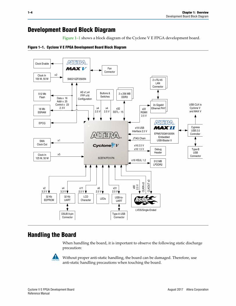
Development Board Block DiagramFigure 1–1 shows a block diagram of the Cyclone V E FPGA development board.
Handling the BoardWhen handling the board, it is important to observe the following static discharge precaution:
c Without proper anti-static handling, the board can be damaged. Therefore, use anti-static handling precautions when touching the board.
Figure 1–1. Cyclone V E FPGA Development Board Block Diagram
5CEFA7F31I7N
N
Data x 16Addr x 25
Control x 232.5V
JTAG Chain
LEDs
Clock In125 M, 50 M
Clock In100 M, 50 M
Debug Header
DSUB 9-pinConnector
x5
x1
x2
EPCQ
5M2210ZF256I5N
CLK
IN x
3
CLK
OU
T x3
LVDS/Single-EndedType-A USB
Connector
x80
2.5
V
x312.5 V
x62.5 V
x42.5 V
x42.5 V
x16 2.5 Vx16 1.5 V
x16 HSUL 1.2
x22RGMII2.5 V
x19 USBInterface 2.5 V
x32SSTL - 15
x112.5 V
x43.3 V
x23.3 V
USB-to-UART
LCDCharacter
32 KbUART
32 KbEEPROM
SMAClock Out
18 MbSSRAM
512 MbFlash
Clock Enable
FanConnector
AS x1,x4FPP x16
Configuration
Buttons &Switches
2 x 256 MBDDR3
EPM570GM100I5NEmbedded
USB-Blaster II
2 x RJ-45 LAN
Connector
USB CLK toCyclone V and MAX V
CypressUSB 2.0
Controller
Type-BUSB
Connector
512 MBLPDDR2
2x GigabitEthernet PHY
Cyclone V E FPGA Development Board August 2017 Altera CorporationReference Manual
August 2017 Altera Corporation
2. Board Components
This chapter introduces the major components on the Cyclone V E FPGA development board. Figure 2–1 illustrates the component locations and Table 2–1 provides a brief description of all component features of the board.
1 A complete set of schematics, a physical layout database, and GERBER files for the development board reside in the Cyclone V E FPGA development kit documents directory.
f For information about powering up the board and installing the demonstration software, refer to the Cyclone V E FPGA Development Kit User Guide.
This chapter consists of the following sections:
■ “Board Overview”
■ “Featured Device: Cyclone V E FPGA” on page 2–4
■ “MAX V CPLD 5M2210 System Controller” on page 2–5
■ “FPGA Configuration” on page 2–10
■ “Clock Circuitry” on page 2–18
■ “General User Input/Output” on page 2–20
■ “Components and Interfaces” on page 2–24
■ “Memory” on page 2–32
■ “Power Supply” on page 2–41
Cyclone V E FPGA Development BoardReference Manual
2–2 Chapter 2: Board ComponentsBoard Overview
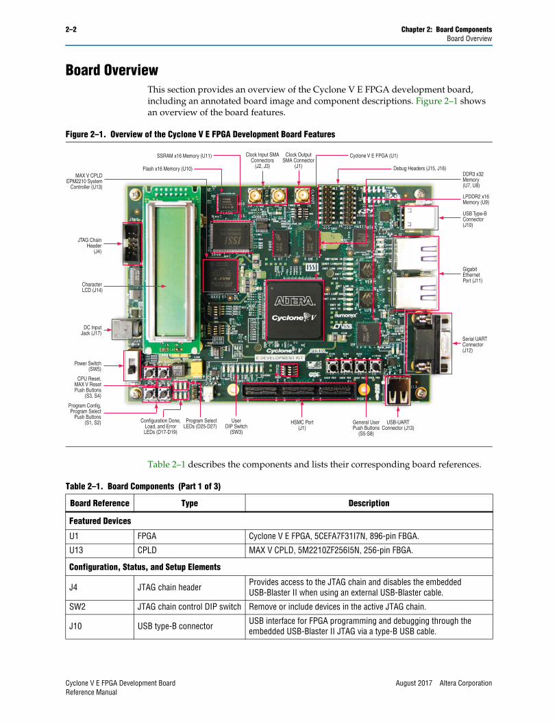
Board OverviewThis section provides an overview of the Cyclone V E FPGA development board, including an annotated board image and component descriptions. Figure 2–1 shows an overview of the board features.
Table 2–1 describes the components and lists their corresponding board references.
Figure 2–1. Overview of the Cyclone V E FPGA Development Board Features
Clock Input SMAConnectors
(J2, J3)
General UserPush Buttons
(S5-S8)
Flash x16 Memory (U10)
LPDDR2 x16Memory (U9)
Serial UARTConnector(J12)
DDR3 x32Memory(U7, U8)
DC InputJack (J17)
CharacterLCD (J14)
CPU Reset,MAX V ResetPush Buttons
(S3, S4)
Power Switch(SW5)
UserDIP Switch
(SW3)
MAX V CPLDEPM2210 System
Controller (U13)
Clock OutputSMA Connector
(J1)
HSMC Port(J1)
Configuration Done,Load, and ErrorLEDs (D17-D19)
Program Config,Program Select
Push Buttons(S1, S2) Program Select
LEDs (D25-D27)
USB Type-BConnector(J10)
USB-UARTConnector (J13)
SSRAM x16 Memory (U11)
Debug Headers (J15, J16)
GigabitEthernetPort (J11)
JTAG ChainHeader
(J4)
Cyclone V E FPGA (U1)
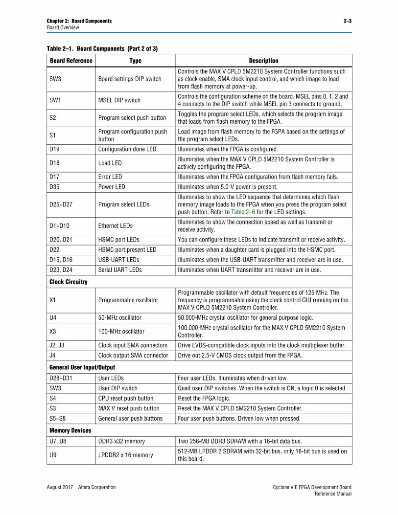
Table 2–1. Board Components (Part 1 of 3)
Board Reference Type Description
Featured Devices
U1 FPGA Cyclone V E FPGA, 5CEFA7F31I7N, 896-pin FBGA.
U13 CPLD MAX V CPLD, 5M2210ZF256I5N, 256-pin FBGA.
Configuration, Status, and Setup Elements
J4 JTAG chain header Provides access to the JTAG chain and disables the embedded USB-Blaster II when using an external USB-Blaster cable.
SW2 JTAG chain control DIP switch Remove or include devices in the active JTAG chain.
J10 USB type-B connector USB interface for FPGA programming and debugging through the embedded USB-Blaster II JTAG via a type-B USB cable.
Cyclone V E FPGA Development Board August 2017 Altera CorporationReference Manual
Chapter 2: Board Components 2–3Board Overview
SW3 Board settings DIP switchControls the MAX V CPLD 5M2210 System Controller functions such as clock enable, SMA clock input control, and which image to load from flash memory at power-up.
SW1 MSEL DIP switch Controls the configuration scheme on the board. MSEL pins 0, 1, 2 and 4 connects to the DIP switch while MSEL pin 3 connects to ground.
S2 Program select push button Toggles the program select LEDs, which selects the program image that loads from flash memory to the FPGA.
S1 Program configuration push button
Load image from flash memory to the FGPA based on the settings of the program select LEDs.
D19 Configuration done LED Illuminates when the FPGA is configured.
D18 Load LED Illuminates when the MAX V CPLD 5M2210 System Controller is actively configuring the FPGA.
D17 Error LED Illuminates when the FPGA configuration from flash memory fails.
D35 Power LED Illuminates when 5.0-V power is present.
D25~D27 Program select LEDsIlluminates to show the LED sequence that determines which flash memory image loads to the FPGA when you press the program select push button. Refer to Table 2–6 for the LED settings.
D1~D10 Ethernet LEDs Illuminates to show the connection speed as well as transmit or receive activity.
D20, D21 HSMC port LEDs You can configure these LEDs to indicate transmit or receive activity.
D22 HSMC port present LED Illuminates when a daughter card is plugged into the HSMC port.
D15, D16 USB-UART LEDs Illuminates when the USB-UART transmitter and receiver are in use.
D23, D24 Serial UART LEDs Illuminates when UART transmitter and receiver are in use.
Clock Circuitry
X1 Programmable oscillatorProgrammable oscillator with default frequencies of 125 MHz. The frequency is programmable using the clock control GUI running on the MAX V CPLD 5M2210 System Controller.
U4 50-MHz oscillator 50.000-MHz crystal oscillator for general purpose logic.
X3 100-MHz oscillator 100.000-MHz crystal oscillator for the MAX V CPLD 5M2210 System Controller.
J2, J3 Clock input SMA connectors Drive LVDS-compatible clock inputs into the clock multiplexer buffer.
J4 Clock output SMA connector Drive out 2.5-V CMOS clock output from the FPGA.
General User Input/Output
D28~D31 User LEDs Four user LEDs. Illuminates when driven low.
SW3 User DIP switch Quad user DIP switches. When the switch is ON, a logic 0 is selected.
S4 CPU reset push button Reset the FPGA logic.
S3 MAX V reset push button Reset the MAX V CPLD 5M2210 System Controller.
S5~S8 General user push buttons Four user push buttons. Driven low when pressed.
Memory Devices
U7, U8 DDR3 x32 memory Two 256-MB DDR3 SDRAM with a 16-bit data bus.
U9 LPDDR2 x 16 memory 512-MB LPDDR 2 SDRAM with 32-bit bus, only 16-bit bus is used on this board.
Table 2–1. Board Components (Part 2 of 3)
Board Reference Type Description
August 2017 Altera Corporation Cyclone V E FPGA Development BoardReference Manual
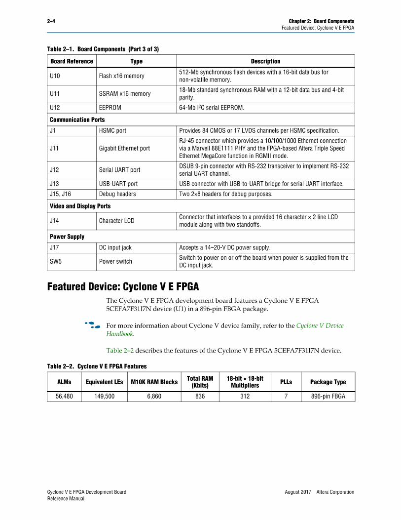
2–4 Chapter 2: Board ComponentsFeatured Device: Cyclone V E FPGA
Featured Device: Cyclone V E FPGAThe Cyclone V E FPGA development board features a Cyclone V E FPGA 5CEFA7F31I7N device (U1) in a 896-pin FBGA package.
f For more information about Cyclone V device family, refer to the Cyclone V Device Handbook.
Table 2–2 describes the features of the Cyclone V E FPGA 5CEFA7F31I7N device.
U10 Flash x16 memory 512-Mb synchronous flash devices with a 16-bit data bus for non-volatile memory.
U11 SSRAM x16 memory 18-Mb standard synchronous RAM with a 12-bit data bus and 4-bit parity.
U12 EEPROM 64-Mb I2C serial EEPROM.
Communication Ports
J1 HSMC port Provides 84 CMOS or 17 LVDS channels per HSMC specification.
J11 Gigabit Ethernet portRJ-45 connector which provides a 10/100/1000 Ethernet connection via a Marvell 88E1111 PHY and the FPGA-based Altera Triple Speed Ethernet MegaCore function in RGMII mode.
J12 Serial UART port DSUB 9-pin connector with RS-232 transceiver to implement RS-232 serial UART channel.
J13 USB-UART port USB connector with USB-to-UART bridge for serial UART interface.
J15, J16 Debug headers Two 2×8 headers for debug purposes.
Video and Display Ports
J14 Character LCD Connector that interfaces to a provided 16 character × 2 line LCD module along with two standoffs.
Power Supply
J17 DC input jack Accepts a 14–20-V DC power supply.
SW5 Power switch Switch to power on or off the board when power is supplied from the DC input jack.
Table 2–1. Board Components (Part 3 of 3)
Board Reference Type Description
Table 2–2. Cyclone V E FPGA Features
ALMs Equivalent LEs M10K RAM Blocks Total RAM (Kbits)
18-bit × 18-bit Multipliers PLLs Package Type
56,480 149,500 6,860 836 312 7 896-pin FBGA
Cyclone V E FPGA Development Board August 2017 Altera CorporationReference Manual
Chapter 2: Board Components 2–5MAX V CPLD 5M2210 System Controller
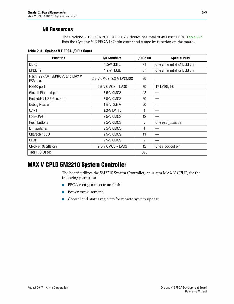
I/O ResourcesThe Cyclone V E FPGA 5CEFA7F31I7N device has total of 480 user I/Os. Table 2–3 lists the Cyclone V E FPGA I/O pin count and usage by function on the board.
MAX V CPLD 5M2210 System Controller The board utilizes the 5M2210 System Controller, an Altera MAX V CPLD, for the following purposes:
■ FPGA configuration from flash
■ Power measurement
■ Control and status registers for remote system update
Table 2–3. Cyclone V E FPGA I/O Pin Count
Function I/O Standard I/O Count Special Pins
DDR3 1.5-V SSTL 71 One differential x4 DQS pin
LPDDR2 1.2-V HSUL 37 One differential x2 DQS pin
Flash, SSRAM, EEPROM, and MAX V FSM bus 2.5-V CMOS, 3.3-V LVCMOS 69 —
HSMC port 2.5-V CMOS + LVDS 79 17 LVDS, I2C
Gigabit Ethernet port 2.5-V CMOS 42 —
Embedded USB-Blaster II 2.5-V CMOS 20 —
Debug Header 1.5-V, 2.5-V 20 —
UART 3.3-V LVTTL 4 —
USB-UART 2.5-V CMOS 12 —
Push buttons 2.5-V CMOS 5 One DEV_CLRn pin
DIP switches 2.5-V CMOS 4 —
Character LCD 2.5-V CMOS 11 —
LEDs 2.5-V CMOS 9 —
Clock or Oscillators 2.5-V CMOS + LVDS 12 One clock out pin
Total I/O Used: 395
August 2017 Altera Corporation Cyclone V E FPGA Development BoardReference Manual
2–6 Chapter 2: Board ComponentsMAX V CPLD 5M2210 System Controller
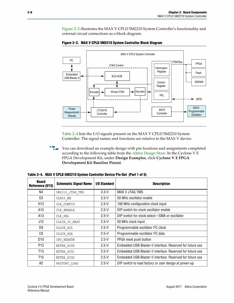
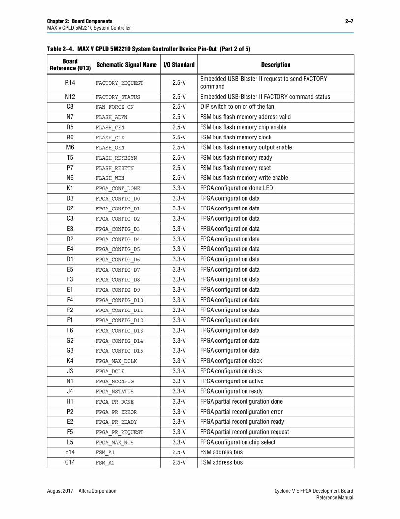
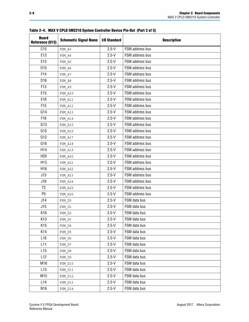
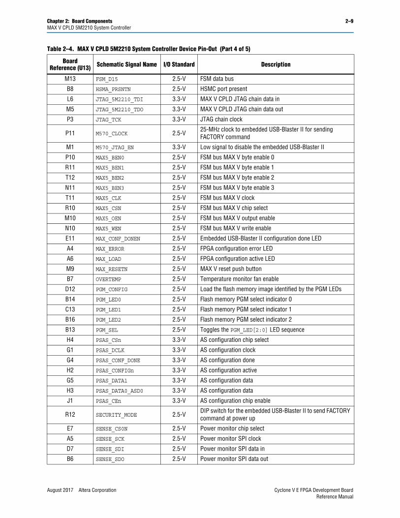
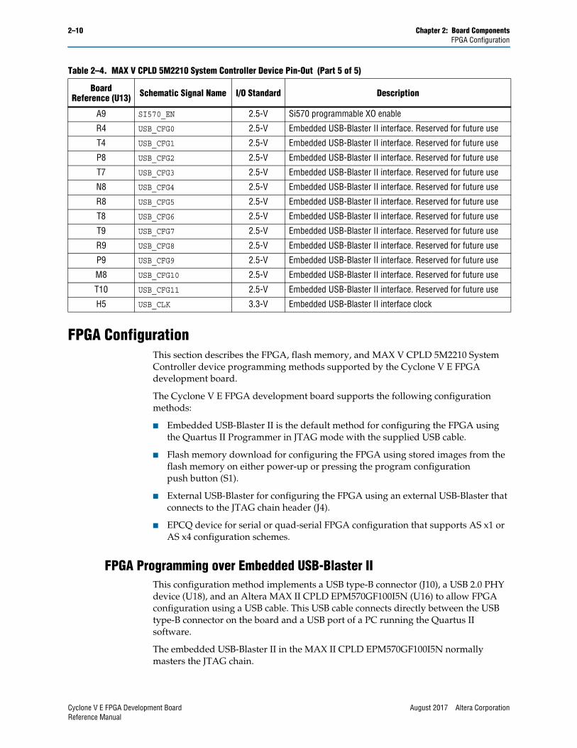
Figure 2–2 illustrates the MAX V CPLD 5M2210 System Controller's functionality and external circuit connections as a block diagram.
Table 2–4 lists the I/O signals present on the MAX V CPLD 5M2210 System Controller. The signal names and functions are relative to the MAX V device.
f You can download an example design with pin locations and assignments completed according to the following table from the Altera Design Store. In the Cyclone V E FPGA Development Kit, under Design Examples, click Cyclone V E FPGA Development Kit Baseline Pinout.
Figure 2–2. MAX V CPLD 5M2210 System Controller Block Diagram
Information Register
EmbeddedUSB-Blaster II
Si570Controller
SLD-HUB
PFL
FSM Bus
MAX V CPLD System Controller
PowerMeasurement
Results
Virtual-JTAG
PCFPGA
LTC2418Controller
Flash
DecoderEncoder
GPIO
JTAG Control
SSRAMControlRegister
Si570 Programmable
Oscillator
Table 2–4. MAX V CPLD 5M2210 System Controller Device Pin-Out (Part 1 of 5)
Board Reference (U13) Schematic Signal Name I/O Standard Description
N4 5M2210_JTAG_TMS 3.3-V MAX V JTAG TMS
E9 CLK50_EN 2.5-V 50 MHz oscillator enable
H12 CLK_CONFIG 2.5-V 100 MHz configuration clock input
A15 CLK_ENABLE 2.5-V DIP switch for clock oscillator enable
A13 CLK_SEL 2.5-V DIP switch for clock select—SMA or oscillator
J12 CLKIN_50_MAXV 2.5-V 50 MHz clock input
D9 CLOCK_SCL 2.5-V Programmable oscillator I2C clock
C9 CLOCK_SDA 2.5-V Programmable oscillator I2C data
D10 CPU_RESETN 2.5-V FPGA reset push button
P12 EXTRA_SIG0 2.5-V Embedded USB-Blaster II interface. Reserved for future use
T13 EXTRA_SIG1 2.5-V Embedded USB-Blaster II interface. Reserved for future use
T15 EXTRA_SIG2 2.5-V Embedded USB-Blaster II interface. Reserved for future use
A2 FACTORY_LOAD 2.5-V DIP switch to load factory or user design at power-up
Cyclone V E FPGA Development Board August 2017 Altera CorporationReference Manual
Chapter 2: Board Components 2–7MAX V CPLD 5M2210 System Controller
R14 FACTORY_REQUEST 2.5-V Embedded USB-Blaster II request to send FACTORY command
N12 FACTORY_STATUS 2.5-V Embedded USB-Blaster II FACTORY command status
C8 FAN_FORCE_ON 2.5-V DIP switch to on or off the fan
N7 FLASH_ADVN 2.5-V FSM bus flash memory address valid
R5 FLASH_CEN 2.5-V FSM bus flash memory chip enable
R6 FLASH_CLK 2.5-V FSM bus flash memory clock
M6 FLASH_OEN 2.5-V FSM bus flash memory output enable
T5 FLASH_RDYBSYN 2.5-V FSM bus flash memory ready
P7 FLASH_RESETN 2.5-V FSM bus flash memory reset
N6 FLASH_WEN 2.5-V FSM bus flash memory write enable
K1 FPGA_CONF_DONE 3.3-V FPGA configuration done LED
D3 FPGA_CONFIG_D0 3.3-V FPGA configuration data
C2 FPGA_CONFIG_D1 3.3-V FPGA configuration data
C3 FPGA_CONFIG_D2 3.3-V FPGA configuration data
E3 FPGA_CONFIG_D3 3.3-V FPGA configuration data
D2 FPGA_CONFIG_D4 3.3-V FPGA configuration data
E4 FPGA_CONFIG_D5 3.3-V FPGA configuration data
D1 FPGA_CONFIG_D6 3.3-V FPGA configuration data
E5 FPGA_CONFIG_D7 3.3-V FPGA configuration data
F3 FPGA_CONFIG_D8 3.3-V FPGA configuration data
E1 FPGA_CONFIG_D9 3.3-V FPGA configuration data
F4 FPGA_CONFIG_D10 3.3-V FPGA configuration data
F2 FPGA_CONFIG_D11 3.3-V FPGA configuration data
F1 FPGA_CONFIG_D12 3.3-V FPGA configuration data
F6 FPGA_CONFIG_D13 3.3-V FPGA configuration data
G2 FPGA_CONFIG_D14 3.3-V FPGA configuration data
G3 FPGA_CONFIG_D15 3.3-V FPGA configuration data
K4 FPGA_MAX_DCLK 3.3-V FPGA configuration clock
J3 FPGA_DCLK 3.3-V FPGA configuration clock
N1 FPGA_NCONFIG 3.3-V FPGA configuration active
J4 FPGA_NSTATUS 3.3-V FPGA configuration ready
H1 FPGA_PR_DONE 3.3-V FPGA partial reconfiguration done
P2 FPGA_PR_ERROR 3.3-V FPGA partial reconfiguration error
E2 FPGA_PR_READY 3.3-V FPGA partial reconfiguration ready
F5 FPGA_PR_REQUEST 3.3-V FPGA partial reconfiguration request
L5 FPGA_MAX_NCS 3.3-V FPGA configuration chip select
E14 FSM_A1 2.5-V FSM address bus
C14 FSM_A2 2.5-V FSM address bus
Table 2–4. MAX V CPLD 5M2210 System Controller Device Pin-Out (Part 2 of 5)
Board Reference (U13) Schematic Signal Name I/O Standard Description
August 2017 Altera Corporation Cyclone V E FPGA Development BoardReference Manual
2–8 Chapter 2: Board ComponentsMAX V CPLD 5M2210 System Controller
C15 FSM_A3 2.5-V FSM address bus
E13 FSM_A4 2.5-V FSM address bus
E12 FSM_A5 2.5-V FSM address bus
D15 FSM_A6 2.5-V FSM address bus
F14 FSM_A7 2.5-V FSM address bus
D16 FSM_A8 2.5-V FSM address bus
F13 FSM_A9 2.5-V FSM address bus
E15 FSM_A10 2.5-V FSM address bus
E16 FSM_A11 2.5-V FSM address bus
F15 FSM_A12 2.5-V FSM address bus
G14 FSM_A13 2.5-V FSM address bus
F16 FSM_A14 2.5-V FSM address bus
G13 FSM_A15 2.5-V FSM address bus
G15 FSM_A16 2.5-V FSM address bus
G12 FSM_A17 2.5-V FSM address bus
G16 FSM_A18 2.5-V FSM address bus
H14 FSM_A19 2.5-V FSM address bus
H20 FSM_A20 2.5-V FSM address bus
H13 FSM_A21 2.5-V FSM address bus
H16 FSM_A22 2.5-V FSM address bus
J13 FSM_A23 2.5-V FSM address bus
J16 FSM_A24 2.5-V FSM address bus
T2 FSM_A25 2.5-V FSM address bus
P5 FSM_A26 2.5-V FSM address bus
J14 FSM_D0 2.5-V FSM data bus
J15 FSM_D1 2.5-V FSM data bus
K16 FSM_D2 2.5-V FSM data bus
K13 FSM_D3 2.5-V FSM data bus
K15 FSM_D4 2.5-V FSM data bus
K14 FSM_D5 2.5-V FSM data bus
L16 FSM_D6 2.5-V FSM data bus
L11 FSM_D7 2.5-V FSM data bus
L15 FSM_D8 2.5-V FSM data bus
L12 FSM_D9 2.5-V FSM data bus
M16 FSM_D10 2.5-V FSM data bus
L13 FSM_D11 2.5-V FSM data bus
M15 FSM_D12 2.5-V FSM data bus
L14 FSM_D13 2.5-V FSM data bus
N16 FSM_D14 2.5-V FSM data bus
Table 2–4. MAX V CPLD 5M2210 System Controller Device Pin-Out (Part 3 of 5)
Board Reference (U13) Schematic Signal Name I/O Standard Description
Cyclone V E FPGA Development Board August 2017 Altera CorporationReference Manual
Chapter 2: Board Components 2–9MAX V CPLD 5M2210 System Controller
M13 FSM_D15 2.5-V FSM data bus
B8 HSMA_PRSNTN 2.5-V HSMC port present
L6 JTAG_5M2210_TDI 3.3-V MAX V CPLD JTAG chain data in
M5 JTAG_5M2210_TDO 3.3-V MAX V CPLD JTAG chain data out
P3 JTAG_TCK 3.3-V JTAG chain clock
P11 M570_CLOCK 2.5-V 25-MHz clock to embedded USB-Blaster II for sending FACTORY command
M1 M570_JTAG_EN 3.3-V Low signal to disable the embedded USB-Blaster II
P10 MAX5_BEN0 2.5-V FSM bus MAX V byte enable 0
R11 MAX5_BEN1 2.5-V FSM bus MAX V byte enable 1
T12 MAX5_BEN2 2.5-V FSM bus MAX V byte enable 2
N11 MAX5_BEN3 2.5-V FSM bus MAX V byte enable 3
T11 MAX5_CLK 2.5-V FSM bus MAX V clock
R10 MAX5_CSN 2.5-V FSM bus MAX V chip select
M10 MAX5_OEN 2.5-V FSM bus MAX V output enable
N10 MAX5_WEN 2.5-V FSM bus MAX V write enable
E11 MAX_CONF_DONEN 2.5-V Embedded USB-Blaster II configuration done LED
A4 MAX_ERROR 2.5-V FPGA configuration error LED
A6 MAX_LOAD 2.5-V FPGA configuration active LED
M9 MAX_RESETN 2.5-V MAX V reset push button
B7 OVERTEMP 2.5-V Temperature monitor fan enable
D12 PGM_CONFIG 2.5-V Load the flash memory image identified by the PGM LEDs
B14 PGM_LED0 2.5-V Flash memory PGM select indicator 0
C13 PGM_LED1 2.5-V Flash memory PGM select indicator 1
B16 PGM_LED2 2.5-V Flash memory PGM select indicator 2
B13 PGM_SEL 2.5-V Toggles the PGM_LED[2:0] LED sequence
H4 PSAS_CSn 3.3-V AS configuration chip select
G1 PSAS_DCLK 3.3-V AS configuration clock
G4 PSAS_CONF_DONE 3.3-V AS configuration done
H2 PSAS_CONFIGn 3.3-V AS configuration active
G5 PSAS_DATA1 3.3-V AS configuration data
H3 PSAS_DATA0_ASD0 3.3-V AS configuration data
J1 PSAS_CEn 3.3-V AS configuration chip enable
R12 SECURITY_MODE 2.5-V DIP switch for the embedded USB-Blaster II to send FACTORY command at power up
E7 SENSE_CS0N 2.5-V Power monitor chip select
A5 SENSE_SCK 2.5-V Power monitor SPI clock
D7 SENSE_SDI 2.5-V Power monitor SPI data in
B6 SENSE_SDO 2.5-V Power monitor SPI data out
Table 2–4. MAX V CPLD 5M2210 System Controller Device Pin-Out (Part 4 of 5)
Board Reference (U13) Schematic Signal Name I/O Standard Description
August 2017 Altera Corporation Cyclone V E FPGA Development BoardReference Manual
2–10 Chapter 2: Board ComponentsFPGA Configuration
FPGA ConfigurationThis section describes the FPGA, flash memory, and MAX V CPLD 5M2210 System Controller device programming methods supported by the Cyclone V E FPGA development board.
The Cyclone V E FPGA development board supports the following configuration methods:
■ Embedded USB-Blaster II is the default method for configuring the FPGA using the Quartus II Programmer in JTAG mode with the supplied USB cable.
■ Flash memory download for configuring the FPGA using stored images from the flash memory on either power-up or pressing the program configuration push button (S1).
■ External USB-Blaster for configuring the FPGA using an external USB-Blaster that connects to the JTAG chain header (J4).
■ EPCQ device for serial or quad-serial FPGA configuration that supports AS x1 or AS x4 configuration schemes.
FPGA Programming over Embedded USB-Blaster IIThis configuration method implements a USB type-B connector (J10), a USB 2.0 PHY device (U18), and an Altera MAX II CPLD EPM570GF100I5N (U16) to allow FPGA configuration using a USB cable. This USB cable connects directly between the USB type-B connector on the board and a USB port of a PC running the Quartus II software.
The embedded USB-Blaster II in the MAX II CPLD EPM570GF100I5N normally masters the JTAG chain.
A9 SI570_EN 2.5-V Si570 programmable XO enable
R4 USB_CFG0 2.5-V Embedded USB-Blaster II interface. Reserved for future use
T4 USB_CFG1 2.5-V Embedded USB-Blaster II interface. Reserved for future use
P8 USB_CFG2 2.5-V Embedded USB-Blaster II interface. Reserved for future use
T7 USB_CFG3 2.5-V Embedded USB-Blaster II interface. Reserved for future use
N8 USB_CFG4 2.5-V Embedded USB-Blaster II interface. Reserved for future use
R8 USB_CFG5 2.5-V Embedded USB-Blaster II interface. Reserved for future use
T8 USB_CFG6 2.5-V Embedded USB-Blaster II interface. Reserved for future use
T9 USB_CFG7 2.5-V Embedded USB-Blaster II interface. Reserved for future use
R9 USB_CFG8 2.5-V Embedded USB-Blaster II interface. Reserved for future use
P9 USB_CFG9 2.5-V Embedded USB-Blaster II interface. Reserved for future use
M8 USB_CFG10 2.5-V Embedded USB-Blaster II interface. Reserved for future use
T10 USB_CFG11 2.5-V Embedded USB-Blaster II interface. Reserved for future use
H5 USB_CLK 3.3-V Embedded USB-Blaster II interface clock
Table 2–4. MAX V CPLD 5M2210 System Controller Device Pin-Out (Part 5 of 5)
Board Reference (U13) Schematic Signal Name I/O Standard Description
Cyclone V E FPGA Development Board August 2017 Altera CorporationReference Manual
Chapter 2: Board Components 2–11FPGA Configuration
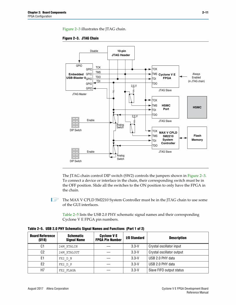
Figure 2–3 illustrates the JTAG chain.
The JTAG chain control DIP switch (SW2) controls the jumpers shown in Figure 2–3. To connect a device or interface in the chain, their corresponding switch must be in the OFF position. Slide all the switches to the ON position to only have the FPGA in the chain.
1 The MAX V CPLD 5M2210 System Controller must be in the JTAG chain to use some of the GUI interfaces.
Table 2–5 lists the USB 2.0 PHY schematic signal names and their corresponding Cyclone V E FPGA pin numbers.
Figure 2–3. JTAG Chain
EmbeddedUSB-Blaster II
GPIOTCK
Cyclone V EFPGA
AnalogSwitch
MAX V CPLD5M2210System
Controller
HSMCPort
GPIOTMS
GPIOTDO
GPIO
GPIO
TDI
JTAG Master
GPIO
Disable
Enable
Enable JTAG Slave
HSMC
TCK
TMS
TDI
TDO
TCK
2.5 V
TMS
TDI
TDO
TCK
TMS
TDI
TDO
JTAG Slave
JTAG Slave
AnalogSwitch
AlwaysEnabled
(in JTAG chain)
DIP Switch
DIP Switch
10-pinJTAG Header
FlashMemory
2.5 V
Table 2–5. USB 2.0 PHY Schematic Signal Names and Functions (Part 1 of 2)
Board Reference (U18)
SchematicSignal Name
Cyclone V E FPGA Pin Number I/O Standard Description
C1 24M_XTALIN — 3.3-V Crystal oscillator input
C2 24M_XTALOUT — 3.3-V Crystal oscillator output
E1 FX2_D_N — 3.3-V USB 2.0 PHY data
E2 FX2_D_P — 3.3-V USB 2.0 PHY data
H7 FX2_FLAGA — 3.3-V Slave FIFO output status
August 2017 Altera Corporation Cyclone V E FPGA Development BoardReference Manual
2–12 Chapter 2: Board ComponentsFPGA Configuration
G7 FX2_FLAGB — 3.3-V Slave FIFO output status
H8 FX2_FLAGC — 3.3-V Slave FIFO output status
G6 FX2_PA1 — 3.3-V USB 2.0 PHY port A interface
F8 FX2_PA2 — 3.3-V USB 2.0 PHY port A interface
F7 FX2_PA3 — 3.3-V USB 2.0 PHY port A interface
F6 FX2_PA4 — 3.3-V USB 2.0 PHY port A interface
C8 FX2_PA5 — 3.3-V USB 2.0 PHY port A interface
C7 FX2_PA6 — 3.3-V USB 2.0 PHY port A interface
C6 FX2_PA7 — 3.3-V USB 2.0 PHY port A interface
H3 FX2_PB0 — 3.3-V USB 2.0 PHY port B interface
F4 FX2_PB1 — 3.3-V USB 2.0 PHY port B interface
H4 FX2_PB2 — 3.3-V USB 2.0 PHY port B interface
G4 FX2_PB3 — 3.3-V USB 2.0 PHY port B interface
H5 FX2_PB4 — 3.3-V USB 2.0 PHY port B interface
G5 FX2_PB5 — 3.3-V USB 2.0 PHY port B interface
F5 FX2_PB6 — 3.3-V USB 2.0 PHY port B interface
H6 FX2_PB7 — 3.3-V USB 2.0 PHY port B interface
A8 FX2_PD0 — 3.3-V USB 2.0 PHY port D interface
A7 FX2_PD1 — 3.3-V USB 2.0 PHY port D interface
B6 FX2_PD2 — 3.3-V USB 2.0 PHY port D interface
A6 FX2_PD3 — 3.3-V USB 2.0 PHY port D interface
B3 FX2_PD4 — 3.3-V USB 2.0 PHY port D interface
A3 FX2_PD5 — 3.3-V USB 2.0 PHY port D interface
C3 FX2_PD6 — 3.3-V USB 2.0 PHY port D interface
A2 FX2_PD7 — 3.3-V USB 2.0 PHY port D interface
B8 FX2_RESETN V21 3.3-V Embedded USB-Blaster hard reset
F3 FX2_SCL — 3.3-V USB 2.0 PHY serial clock
G3 FX2_SDA — 3.3-V USB 2.0 PHY serial data
A1 FX2_SLRDN — 3.3-V Read strobe for slave FIFO
B1 FX2_SLWRN — 3.3-V Write strobe for slave FIFO
B7 FX2_WAKEUP — 3.3-V USB 2.0 PHY wake signal
G2 USB_CLK AA23 3.3-V USB 2.0 PHY 48-MHz interface clock
Table 2–5. USB 2.0 PHY Schematic Signal Names and Functions (Part 2 of 2)
Board Reference (U18)
SchematicSignal Name
Cyclone V E FPGA Pin Number I/O Standard Description
Cyclone V E FPGA Development Board August 2017 Altera CorporationReference Manual
Chapter 2: Board Components 2–13FPGA Configuration
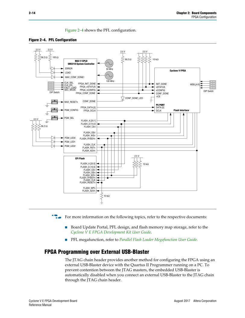
FPGA Programming from Flash MemoryFlash memory programming is possible through a variety of methods. The default method is to use the factory design—Board Update Portal. This design is an embedded webserver, which serves the Board Update Portal web page. The web page allows you to select new FPGA designs including hardware, software, or both in an industry-standard S-Record File (.flash) and write the design to the user hardware page (page 1) of the flash memory over the network.
The secondary method is to use the pre-built parallel flash loader (PFL) design included in the development kit. The development board implements the Altera PFL megafunction for flash memory programming. The PFL megafunction is a block of logic that is programmed into an Altera programmable logic device (FPGA or CPLD). The PFL functions as a utility for writing to a compatible flash memory device. This pre-built design contains the PFL megafunction that allows you to write either page 0, page 1, or other areas of flash memory over the USB interface using the Quartus II software. This method is used to restore the development board to its factory default settings.
Other methods to program the flash memory can be used as well, including the Nios® II processor.
f For more information on the Nios II processor, refer to the Nios II Processor page of the Altera website.
On either power-up or by pressing the program configuration push button, PGM_CONFIG (S1), the MAX V CPLD 5M2210 System Controller's PFL configures the FPGA from the flash memory. The PFL megafunction reads 16-bit data from the flash memory and converts it to fast passive parallel (FPP) format. This 16-bit data is then written to the dedicated configuration pins in the FPGA during configuration.
Pressing the PGM_CONFIG push button (S1) loads the FPGA with a hardware page based on which PGM_LED[2:0] (D25, D26, D27) illuminates. Table 2–6 lists the design that loads when you press the PGM_CONFIG push button.
Table 2–6. PGM_LED Settings (1)
PGM_LED0 (D25) PGM_LED1 (D26) PGM_LED2 (D27) Design
ON OFF OFF Factory hardware
OFF ON OFF User hardware 1
OFF OFF ON User hardware 2
Note to Table 2–6:
(1) ON indicates a setting of ’0’ while OFF indicates a setting of ’1’.
August 2017 Altera Corporation Cyclone V E FPGA Development BoardReference Manual
2–14 Chapter 2: Board ComponentsFPGA Configuration
Figure 2–4 shows the PFL configuration.
f For more information on the following topics, refer to the respective documents:
■ Board Update Portal, PFL design, and flash memory map storage, refer to the Cyclone V E FPGA Development Kit User Guide.
■ PFL megafunction, refer to Parallel Flash Loader Megafunction User Guide.
FPGA Programming over External USB-BlasterThe JTAG chain header provides another method for configuring the FPGA using an external USB-Blaster device with the Quartus II Programmer running on a PC. To prevent contention between the JTAG masters, the embedded USB-Blaster is automatically disabled when you connect an external USB-Blaster to the JTAG chain through the JTAG chain header.
Figure 2–4. PFL Configuration
MAX V CPLD5M2210 System Controller
FPGA_DATA [0]FPGA_DCLK
FLASH_A [25:1]FLASH_D [15:0]
DATA [0]DCLK
nSTATUSnCONFIGCONF_DONE
CONF_DONE
MSEL[4:0]
2.5 V
10 kΩ
nCE
CFI Flash
FLASH_CEn
FLASH_OEnFLASH_WEn
FLASH_A [25:0]FLASH_D [15:0]
FLASH_CEnFLASH_OEnFLASH_WEn
FLASH_WPnFLASH_ADVn
FPGA_nCONFIGFPGA_CONF_DONE
FLASH_RYBSYn
FLASH_RYBSYn
FPGA_nSTATUS
2.5 V
10 kΩ
FLASH_ADVn
CONF_DONE_LED
2.5 V
FLASH_CLK
FLASH_CLKFLASH_RSTn
FLASH_RESETn
PS PORT
Flash Interface
56.2 Ω100 Ω56.2 Ω
56.2 Ω
50 MHz
100 MHzINIT_DONEFPGA_INIT_DONE
2.5 V
2.5 V 2.5 V
ERROR
LOAD
MAX_CONF_DONE1
SEC_MODEFACT_LOADCLK_ENCLK_SEL
MAX_RESETn
PGM_CONFIG
PGM_SEL
PGM_LED0
PGM_LED1
PGM_LED2
DIP Switch
10 kΩ
Cyclone V FPGA
DIP Switch
Cyclone V E FPGA Development Board August 2017 Altera CorporationReference Manual
Chapter 2: Board Components 2–15Status Elements
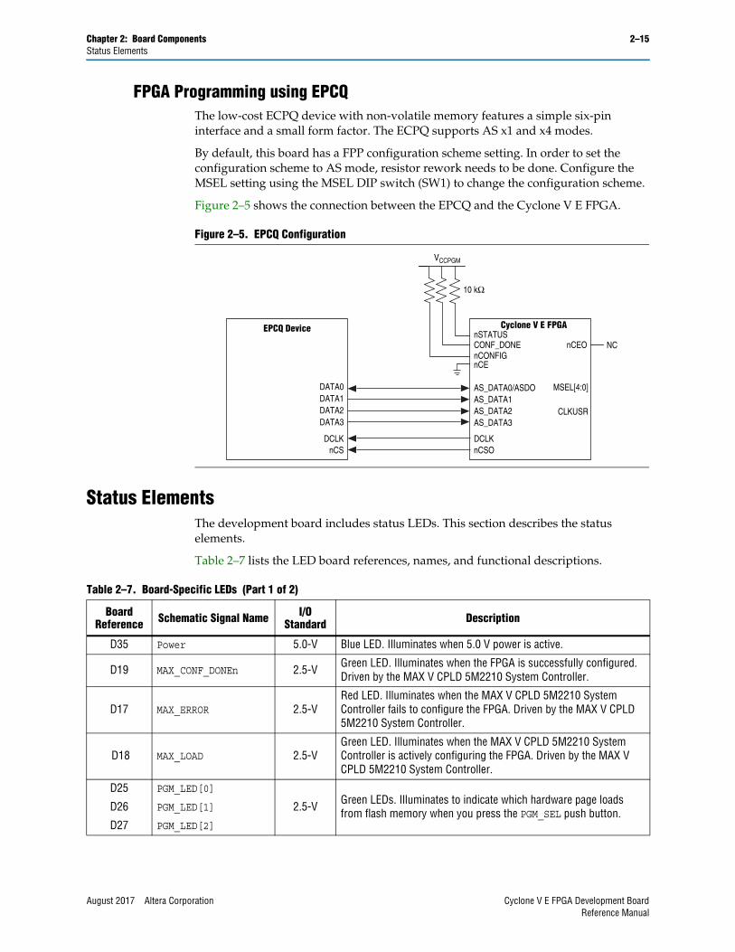
FPGA Programming using EPCQThe low-cost ECPQ device with non-volatile memory features a simple six-pin interface and a small form factor. The ECPQ supports AS x1 and x4 modes.
By default, this board has a FPP configuration scheme setting. In order to set the configuration scheme to AS mode, resistor rework needs to be done. Configure the MSEL setting using the MSEL DIP switch (SW1) to change the configuration scheme.
Figure 2–5 shows the connection between the EPCQ and the Cyclone V E FPGA.
Status ElementsThe development board includes status LEDs. This section describes the status elements.
Table 2–7 lists the LED board references, names, and functional descriptions.
Figure 2–5. EPCQ Configuration
EPCQ Device Cyclone V E FPGA
VCCPGM
10 kΩ
DATA0DATA1DATA2DATA3
DCLKnCS
AS_DATA0/ASDOAS_DATA1AS_DATA2AS_DATA3
DCLK
nSTATUSCONF_DONEnCONFIGnCE
nCSO
nCEO NC
MSEL[4:0]
CLKUSR
Table 2–7. Board-Specific LEDs (Part 1 of 2)
Board Reference Schematic Signal Name I/O
Standard Description
D35 Power 5.0-V Blue LED. Illuminates when 5.0 V power is active.
D19 MAX_CONF_DONEn 2.5-V Green LED. Illuminates when the FPGA is successfully configured. Driven by the MAX V CPLD 5M2210 System Controller.
D17 MAX_ERROR 2.5-VRed LED. Illuminates when the MAX V CPLD 5M2210 System Controller fails to configure the FPGA. Driven by the MAX V CPLD 5M2210 System Controller.
D18 MAX_LOAD 2.5-VGreen LED. Illuminates when the MAX V CPLD 5M2210 System Controller is actively configuring the FPGA. Driven by the MAX V CPLD 5M2210 System Controller.
D25
D26
D27
PGM_LED[0]
PGM_LED[1]
PGM_LED[2]
2.5-V Green LEDs. Illuminates to indicate which hardware page loads from flash memory when you press the PGM_SEL push button.
August 2017 Altera Corporation Cyclone V E FPGA Development BoardReference Manual
2–16 Chapter 2: Board ComponentsSetup Elements
Setup ElementsThe development board includes several different kinds of setup elements. This section describes the following setup elements:
■ Board settings DIP switch
■ JTAG settings DIP switch
■ CPU reset push button
■ MAX V reset push button
■ Program configuration push button
■ Program select push button
D11, D12
D13, D14
JTAG_RX, JTAG_TX
SC_RX, SC_TX2.5-V Green LEDs. Illuminates to indicate USB-Blaster II receive and
transmit activities.
D1 ENETA_LED_TX 2.5-V Green LED. Illuminates to indicate Ethernet PHY transmit activity. Driven by the Marvell 88E1111 PHY.
D2 ENETA_LED_RX 2.5-V Green LED. Illuminates to indicate Ethernet PHY receive activity. Driven by the Marvell 88E1111 PHY.
D5 ENETA_LED_LINK10 2.5-V Green LED. Illuminates to indicate Ethernet linked at 10 Mbps connection speed. Driven by the Marvell 88E1111 PHY.
D4 ENETA_LED_LINK100 2.5-V Green LED. Illuminates to indicate Ethernet linked at 100 Mbps connection speed. Driven by the Marvell 88E1111 PHY.
D3 ENETA_LED_LINK1000 2.5-V Green LED. Illuminates to indicate Ethernet linked at 1000 Mbps connection speed. Driven by the Marvell 88E1111 PHY.
D19 ENETB_LED_TX 2.5-V Green LED. Illuminates to indicate Ethernet PHY B transmit activity. Driven by the Marvell 88E1111 PHY.
D22 ENETB_LED_RX 2.5-V Green LED. Illuminates to indicate Ethernet PHY B receive activity. Driven by the Marvell 88E1111 PHY.
D24 ENETB_LED_LINK10 2.5-V Green LED. Illuminates to indicate Ethernet B linked at 10 Mbps connection speed. Driven by the Marvell 88E1111 PHY.
D20 ENETB_LED_LINK100 2.5-V Green LED. Illuminates to indicate Ethernet B linked at 100 Mbps connection speed. Driven by the Marvell 88E1111 PHY.
D21 ENETB_LED_LINK1000 2.5-V Green LED. Illuminates to indicate Ethernet B linked at 1000 Mbps connection speed. Driven by the Marvell 88E1111 PHY.
D15, D16 USB_UART_TX_TOGGLE, USB_UART_RX_TOGGLE
2.5-V Green LED. Illuminates to indicate USB_UART receive and transmit activities.
D23, D24 UART_RXD_LED, UART_TXD_LED
2.5-V Green LED. Illuminates to indicate UART receive and transmit activities.
D3 HSMA_PRSNTn 3.3-VGreen LED. Illuminates when HSMC port has a board or cable plugged-in such that pin 160 becomes grounded. Driven by the add-in card.
Table 2–7. Board-Specific LEDs (Part 2 of 2)
Board Reference Schematic Signal Name I/O
Standard Description
Cyclone V E FPGA Development Board August 2017 Altera CorporationReference Manual
Chapter 2: Board Components 2–17Setup Elements
f For more information about the default settings of the DIP switches, refer to the Cyclone V E FPGA Development Kit User Guide.
Board Settings DIP SwitchThe board settings DIP switch (SW4) controls various features specific to the board and the MAX V CPLD 5M2210 System Controller logic design. Table 2–8 lists the switch controls and descriptions.
JTAG Chain Control DIP SwitchThe JTAG chain control DIP switch (SW2) either removes or includes devices in the active JTAG chain. The Cyclone V E FPGA is always in the JTAG chain. Table 2–9 lists the switch controls and its descriptions.
CPU Reset Push ButtonThe CPU reset push button, CPU_RESETn (S4), is an input to the Cyclone V E FPGA DEV_CLRn pin and is an open-drain I/O from the MAX V CPLD System Controller. This push button is the default reset for both the FPGA and CPLD logic. The MAX V CPLD 5M2210 System Controller also drives this push button during power-on-reset (POR).
Table 2–8. Board Settings DIP Switch Controls
Switch Schematic Signal Name Description
1 CLK_SELON : Select programmable oscillator clock
OFF : Select SMA input clock
2 CLK_ENABLEON : Disable on-board oscillator
OFF : Enable on-board oscillator
3 FACTORY_LOADON : Load the user design from flash at power up
OFF : Load the factory design from flash at power up
4 SECURITY_MODE
ON : Embedded USB-Blaster II sends FACTORY command at power up.
OFF : Embedded USB-Blaster II does not send FACTORY command at power up.
Table 2–9. JTAG Chain Control DIP Switch
Switch Schematic Signal Name Description
1 5M2210_JTAG_ENON : Bypass MAX V CPLD 5M2210 System Controller
OFF : MAX V CPLD 5M2210 System Controller in-chain
2 HSMC_JTAG_ENON : Bypass HSMC port
OFF : HSMC port in-chain
3 FAN_FORCE_ONON : Enable fan
OFF : Disable fan
4 RESERVED Reserved
August 2017 Altera Corporation Cyclone V E FPGA Development BoardReference Manual
2–18 Chapter 2: Board ComponentsClock Circuitry
MAX V Reset Push ButtonThe MAX V reset push button, MAX_RESETn (S3), is an input to the MAX V CPLD 5M2210 System Controller. This push button is the default reset for the CPLD logic.
Program Configuration Push ButtonThe program configuration push button, PGM_CONFIG (S1), is an input to the MAX V CPLD 5M2210 System Controller. This input forces a FPGA reconfiguration from the flash memory. The location in the flash memory is based on the settings of PGM_LED[2:0], which is controlled by the program select push button, PGM_SEL. Valid settings include PGM_LED0, PGM_LED1, or PGM_LED2 on the three pages in flash memory reserved for FPGA designs.
Program Select Push ButtonThe program select push button, PGM_SEL (S2), is an input to the MAX V CPLD 5M2210 System Controller. This push button toggles the PGM_LED[2:0]sequence that selects which location in the flash memory is used to configure the FPGA. Refer to Table 2–6 for the PGM_LED[2:0] sequence definitions.
Clock CircuitryThis section describes the board's clock inputs and outputs.
On-Board OscillatorsThe development board include oscillators with a frequency of 50-MHz, 100-MHz, and a programmable oscillator.
Cyclone V E FPGA Development Board August 2017 Altera CorporationReference Manual
Chapter 2: Board Components 2–19Clock Circuitry
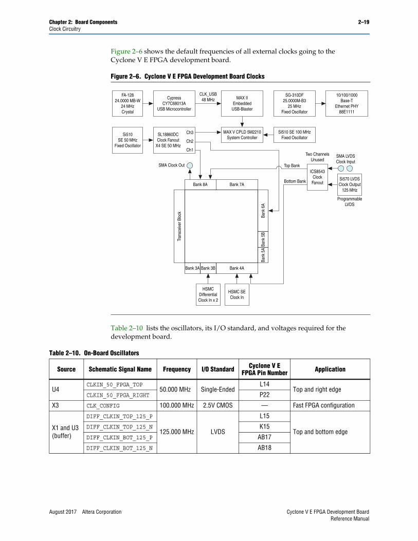
Figure 2–6 shows the default frequencies of all external clocks going to the Cyclone V E FPGA development board.
Table 2–10 lists the oscillators, its I/O standard, and voltages required for the development board.
Figure 2–6. Cyclone V E FPGA Development Board Clocks
FA-12824.0000 MB-W
24 MHzCrystal
CypressCY7C68013A
USB Microcontroller
MAX IIEmbedded
USB-Blaster
Si510SE 50 MHz
Fixed Oscillator
SL18860DCClock Fanout
X4 SE 50 MHz
Ch3
Ch2
Ch1
CLK_USB48 MHz
SG-310DF25.0000M-B3
25 MHzFixed Oscillator
10/100/1000Base-T
Ethernet PHY88E1111
Bank 8A Bank 7A
Bank 3A Bank 3B Bank 4ABa
nk 5
ABa
nk 5
BBa
nk 6
A
Tran
scei
ver B
lock
SMA Clock Out
Two ChannelsUnused
Top Bank
Bottom Bank
SMA LVDSClock Input
Si570 LVDSClock Output
125 MHz
ProgrammableLVDS
HSMCDifferentialClock In x 2
HSMC SEClock In
MAX V CPLD 5M2210System Controller
SI510 SE 100 MHzFixed Oscillator
ICS8543Clock
Fanout
Table 2–10. On-Board Oscillators
Source Schematic Signal Name Frequency I/O Standard Cyclone V E FPGA Pin Number Application
U4CLKIN_50_FPGA_TOP
50.000 MHz Single-EndedL14
Top and right edgeCLKIN_50_FPGA_RIGHT P22
X3 CLK_CONFIG 100.000 MHz 2.5V CMOS — Fast FPGA configuration
X1 and U3 (buffer)
DIFF_CLKIN_TOP_125_P
125.000 MHz LVDS
L15
Top and bottom edgeDIFF_CLKIN_TOP_125_N K15
DIFF_CLKIN_BOT_125_P AB17
DIFF_CLKIN_BOT_125_N AB18
August 2017 Altera Corporation Cyclone V E FPGA Development BoardReference Manual
2–20 Chapter 2: Board ComponentsGeneral User Input/Output
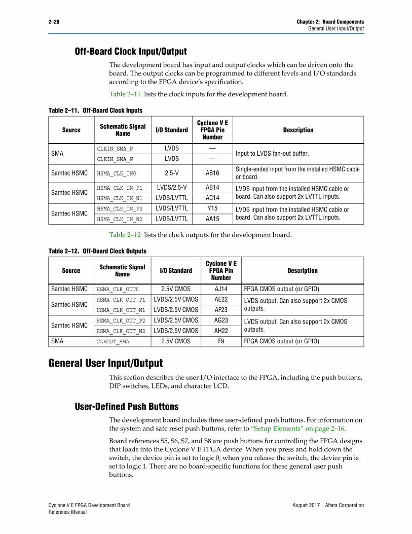
Off-Board Clock Input/OutputThe development board has input and output clocks which can be driven onto the board. The output clocks can be programmed to different levels and I/O standards according to the FPGA device’s specification.
Table 2–11 lists the clock inputs for the development board.
Table 2–12 lists the clock outputs for the development board.
General User Input/OutputThis section describes the user I/O interface to the FPGA, including the push buttons, DIP switches, LEDs, and character LCD.
User-Defined Push ButtonsThe development board includes three user-defined push buttons. For information on the system and safe reset push buttons, refer to “Setup Elements” on page 2–16.
Board references S5, S6, S7, and S8 are push buttons for controlling the FPGA designs that loads into the Cyclone V E FPGA device. When you press and hold down the switch, the device pin is set to logic 0; when you release the switch, the device pin is set to logic 1. There are no board-specific functions for these general user push buttons.
Table 2–11. Off-Board Clock Inputs
Source Schematic Signal Name I/O Standard
Cyclone V E FPGA Pin Number
Description
SMACLKIN_SMA_P LVDS —
Input to LVDS fan-out buffer.CLKIN_SMA_N LVDS —
Samtec HSMC HSMA_CLK_IN0 2.5-V AB16 Single-ended input from the installed HSMC cable or board.
Samtec HSMCHSMA_CLK_IN_P1 LVDS/2.5-V AB14 LVDS input from the installed HSMC cable or
board. Can also support 2x LVTTL inputs.HSMA_CLK_IN_N1 LVDS/LVTTL AC14
Samtec HSMCHSMA_CLK_IN_P2 LVDS/LVTTL Y15 LVDS input from the installed HSMC cable or
board. Can also support 2x LVTTL inputs.HSMA_CLK_IN_N2 LVDS/LVTTL AA15
Table 2–12. Off-Board Clock Outputs
Source Schematic Signal Name I/O Standard
Cyclone V E FPGA Pin Number
Description
Samtec HSMC HSMA_CLK_OUT0 2.5V CMOS AJ14 FPGA CMOS output (or GPIO)
Samtec HSMCHSMA_CLK_OUT_P1 LVDS/2.5V CMOS AE22 LVDS output. Can also support 2x CMOS
outputs.HSMA_CLK_OUT_N1 LVDS/2.5V CMOS AF23
Samtec HSMCHSMA_CLK_OUT_P2 LVDS/2.5V CMOS AG23 LVDS output. Can also support 2x CMOS
outputs.HSMA_CLK_OUT_N2 LVDS/2.5V CMOS AH22
SMA CLKOUT_SMA 2.5V CMOS F9 FPGA CMOS output (or GPIO)
Cyclone V E FPGA Development Board August 2017 Altera CorporationReference Manual
Chapter 2: Board Components 2–21General User Input/Output
Table 2–13 lists the user-defined push button schematic signal names and their corresponding Cyclone V E FPGA pin numbers.
User-Defined DIP SwitchBoard reference SW3 is a four-pin DIP switch. This switch is user-defined and provides additional FPGA input control. When the switch is in the OFF position, a logic 1 is selected. When the switch is in the ON position, a logic 0 is selected. There are no board-specific functions for this switch.
Table 2–14 lists the user-defined DIP switch schematic signal names and their corresponding Cyclone V E FPGA pin numbers.
User-Defined LEDsThe development board includes general and HSMC user-defined LEDs. This section describes all user-defined LEDs. For information on board specific or status LEDs, refer to “Status Elements” on page 2–15.
General LEDsBoard references D28 through D31 are four user-defined LEDs. The status and debugging signals are driven to the LEDs from the designs loaded into the Cyclone V E FPGA. Driving a logic 0 on the I/O port turns the LED on while driving a logic 1 turns the LED off. There are no board-specific functions for these LEDs.
Table 2–13. User-Defined Push Button Schematic Signal Names and Functions
Board Reference Schematic Signal Name Cyclone V E FPGA Pin Number I/O Standard
S5 USER_PB0 AB12 2.5-V
S6 USER_PB1 AB13 2.5-V
S7 USER_PB2 AF13 2.5-V
S8 USER_PB3 AG12 2.5-V
Table 2–14. User-Defined DIP Switch Schematic Signal Names and Functions
Board Reference Schematic Signal Name Cyclone V E FPGAPin Number I/O Standard
1 USER_DIPSW0 Y12 2.5-V
2 USER_DIPSW1 AA13 2.5-V
3 USER_DIPSW2 AF11 2.5-V
4 USER_DIPSW3 AG11 2.5-V
August 2017 Altera Corporation Cyclone V E FPGA Development BoardReference Manual
2–22 Chapter 2: Board ComponentsGeneral User Input/Output
Table 2–15 lists the general LED schematic signal names and their corresponding Cyclone V E FPGA pin numbers.
HSMC LEDsBoard references D20 and D21 are LEDs for the HSMC port. There are no board-specific functions for the HSMC LEDs. The LEDs are labeled TX and RX, and are intended to display data flow to and from the connected daughtercards. The LEDs are driven by the Cyclone V E FPGA device.
Table 2–16 lists the HSMC LED schematic signal names and their corresponding Cyclone V E FPGA pin numbers.
Character LCD The development board includes a single 14-pin 0.1" pitch dual-row header that interfaces to a 2 line × 16 character Lumex character LCD. The character LCD has a 14-pin receptacle that mounts directly to the board's 14-pin header, so it can be easily removed for access to components under the display. You can also use the header for debugging or other purposes.
Table 2–17 summarizes the character LCD pin assignments. The signal names and directions are relative to the Cyclone V E FPGA device.
Table 2–15. General LED Schematic Signal Names and Functions
Board Reference Schematic Signal Name Cyclone V E FPGAPin Number I/O Standard
D28 USER_LED0 AK3 2.5-V
D29 USER_LED1 AJ4 2.5-V
D30 USER_LED2 AJ5 2.5-V
D31 USER_LED3 AK6 2.5-V
Table 2–16. HSMC LED Schematic Signal Names and Functions
Board Reference Schematic Signal Name Cyclone V E FPGA Pin Number I/O Standard
D1 HSMC_RX_LED AH12 2.5-V
D2 HSMC_TX_LED AH11 2.5-V
Table 2–17. Character LCD Pin Assignments, Schematic Signal Names, and Functions
Board Reference (J14) Schematic Signal Name Cyclone V E FPGA
Pin Number I/O Standard Description
7 LCD_DATA0 AJ7 2.5-V LCD data bus
8 LCD_DATA1 AK7 2.5-V LCD data bus
9 LCD_DATA2 AJ8 2.5-V LCD data bus
10 LCD_DATA3 AK8 2.5-V LCD data bus
11 LCD_DATA4 AF9 2.5-V LCD data bus
12 LCD_DATA5 AG9 2.5-V LCD data bus
13 LCD_DATA6 AH9 2.5-V LCD data bus
14 LCD_DATA7 AJ9 2.5-V LCD data bus
Cyclone V E FPGA Development Board August 2017 Altera CorporationReference Manual
Chapter 2: Board Components 2–23General User Input/Output
Table 2–18 lists the LCD pin definitions, and is an excerpt from Lumex data sheet.
f For more information such as timing, character maps, interface guidelines, and other related documentation, visit www.lumex.com.
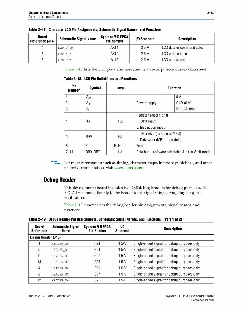
Debug HeaderThis development board includes two 2×8 debug headers for debug purposes. The FPGA I/Os route directly to the header for design testing, debugging, or quick verification.
Table 2–19 summarizes the debug header pin assignments, signal names, and functions.
4 LCD_D_Cn AK11 2.5-V LCD data or command select
5 LCD_WEn AK10 2.5-V LCD write enable
6 LCD_CSn AJ12 2.5-V LCD chip select
Table 2–17. Character LCD Pin Assignments, Schematic Signal Names, and Functions
Board Reference (J14) Schematic Signal Name Cyclone V E FPGA
Pin Number I/O Standard Description
Table 2–18. LCD Pin Definitions and Functions
Pin Number Symbol Level Function
1 VDD —
Power supply
5 V
2 VSS — GND (0 V)
3 V0 — For LCD drive
4 RS H/L
Register select signal
H: Data input
L: Instruction input
5 R/W H/LH: Data read (module to MPU)
L: Data write (MPU to module)
6 E H, H to L Enable
7–14 DB0–DB7 H/L Data bus—software selectable 4-bit or 8-bit mode
Table 2–19. Debug Header Pin Assignments, Schematic Signal Names, and Functions (Part 1 of 2)
Board Reference
Schematic Signal Name
Cyclone V E FPGA Pin Number
I/O Standard Description
Debug Header (J15)
1 HEADER_D0 H21 1.5-V Single-ended signal for debug purposes only
5 HEADER_D1 G21 1.5-V Single-ended signal for debug purposes only
9 HEADER_D2 G22 1.5-V Single-ended signal for debug purposes only
13 HEADER_D3 E26 1.5-V Single-ended signal for debug purposes only
4 HEADER_D4 E25 1.5-V Single-ended signal for debug purposes only
8 HEADER_D5 C27 1.5-V Single-ended signal for debug purposes only
12 HEADER_D6 C26 1.5-V Single-ended signal for debug purposes only
August 2017 Altera Corporation Cyclone V E FPGA Development BoardReference Manual
2–24 Chapter 2: Board ComponentsComponents and Interfaces
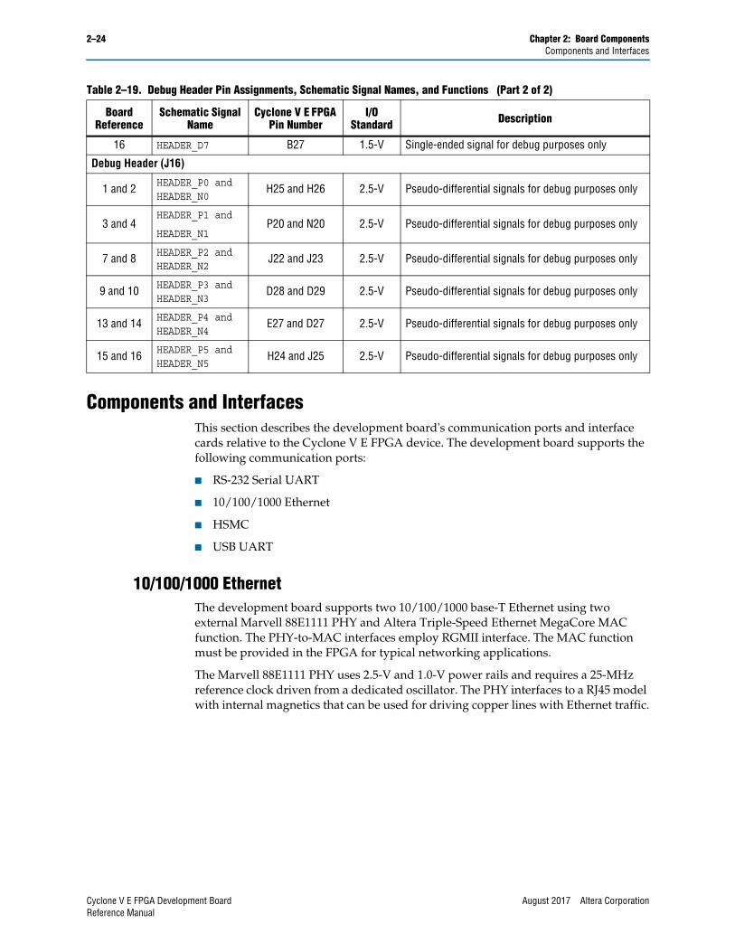
Components and InterfacesThis section describes the development board's communication ports and interface cards relative to the Cyclone V E FPGA device. The development board supports the following communication ports:
■ RS-232 Serial UART
■ 10/100/1000 Ethernet
■ HSMC
■ USB UART
10/100/1000 EthernetThe development board supports two 10/100/1000 base-T Ethernet using two external Marvell 88E1111 PHY and Altera Triple-Speed Ethernet MegaCore MAC function. The PHY-to-MAC interfaces employ RGMII interface. The MAC function must be provided in the FPGA for typical networking applications.
The Marvell 88E1111 PHY uses 2.5-V and 1.0-V power rails and requires a 25-MHz reference clock driven from a dedicated oscillator. The PHY interfaces to a RJ45 model with internal magnetics that can be used for driving copper lines with Ethernet traffic.
16 HEADER_D7 B27 1.5-V Single-ended signal for debug purposes only
Debug Header (J16)
1 and 2 HEADER_P0 and HEADER_N0
H25 and H26 2.5-V Pseudo-differential signals for debug purposes only
3 and 4HEADER_P1 and
HEADER_N1P20 and N20 2.5-V Pseudo-differential signals for debug purposes only
7 and 8 HEADER_P2 and HEADER_N2
J22 and J23 2.5-V Pseudo-differential signals for debug purposes only
9 and 10 HEADER_P3 and HEADER_N3
D28 and D29 2.5-V Pseudo-differential signals for debug purposes only
13 and 14 HEADER_P4 and HEADER_N4
E27 and D27 2.5-V Pseudo-differential signals for debug purposes only
15 and 16 HEADER_P5 and HEADER_N5
H24 and J25 2.5-V Pseudo-differential signals for debug purposes only
Table 2–19. Debug Header Pin Assignments, Schematic Signal Names, and Functions (Part 2 of 2)
Board Reference
Schematic Signal Name
Cyclone V E FPGA Pin Number
I/O Standard Description
Cyclone V E FPGA Development Board August 2017 Altera CorporationReference Manual
Chapter 2: Board Components 2–25Components and Interfaces
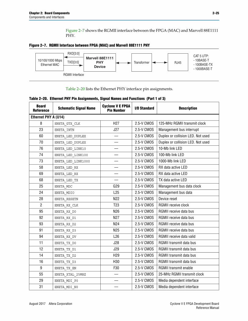
Figure 2–7 shows the RGMII interface between the FPGA (MAC) and Marvell 88E1111 PHY.
Table 2–20 lists the Ethernet PHY interface pin assignments.
Figure 2–7. RGMII Interface between FPGA (MAC) and Marvell 88E1111 PHY
10/100/1000 MbpsEthernet MAC
Marvell 88E1111PHY
DeviceTransformer RJ45
RGMII Interface
TXD[3:0]
RXD[3:0]CAT 5 UTP:- 10BASE-T- 100BASE-TX- 1000BASE-T
Table 2–20. Ethernet PHY Pin Assignments, Signal Names and Functions (Part 1 of 3)
Board Reference Schematic Signal Name Cyclone V E FPGA
Pin Number I/O Standard Description
Ethernet PHY A (U14)
8 ENETA_GTX_CLK H27 2.5-V CMOS 125-MHz RGMII transmit clock
23 ENETA_INTN J27 2.5-V CMOS Management bus interrupt
60 ENETA_LED_DUPLEX — 2.5-V CMOS Duplex or collision LED. Not used
70 ENETA_LED_DUPLEX — 2.5-V CMOS Duplex or collision LED. Not used
76 ENETA_LED_LINK10 — 2.5-V CMOS 10-Mb link LED
74 ENETA_LED_LINK100 — 2.5-V CMOS 100-Mb link LED
73 ENETA_LED_LINK1000 — 2.5-V CMOS 1000-Mb link LED
58 ENETA_LED_RX — 2.5-V CMOS RX data active LED
69 ENETA_LED_RX — 2.5-V CMOS RX data active LED
68 ENETA_LED_TX — 2.5-V CMOS TX data active LED
25 ENETA_MDC G29 2.5-V CMOS Management bus data clock
24 ENETA_MDIO L25 2.5-V CMOS Management bus data
28 ENETA_RESETN N22 2.5-V CMOS Device reset
2 ENETA_RX_CLK T23 2.5-V CMOS RGMII receive clock
95 ENETA_RX_D0 N26 2.5-V CMOS RGMII receive data bus
92 ENETA_RX_D1 N27 2.5-V CMOS RGMII receive data bus
93 ENETA_RX_D2 N24 2.5-V CMOS RGMII receive data bus
91 ENETA_RX_D3 N25 2.5-V CMOS RGMII receive data bus
94 ENETA_RX_DV L26 2.5-V CMOS RGMII receive data valid
11 ENETA_TX_D0 J28 2.5-V CMOS RGMII transmit data bus
12 ENETA_TX_D1 J29 2.5-V CMOS RGMII transmit data bus
14 ENETA_TX_D2 H29 2.5-V CMOS RGMII transmit data bus
16 ENETA_TX_D3 H30 2.5-V CMOS RGMII transmit data bus
9 ENETA_TX_EN F30 2.5-V CMOS RGMII transmit enable
55 ENETA_XTAL_25MHZ — 2.5-V CMOS 25-MHz RGMII transmit clock
29 ENETA_MDI_P0 — 2.5-V CMOS Media dependent interface
31 ENETA_MDI_N0 — 2.5-V CMOS Media dependent interface
August 2017 Altera Corporation Cyclone V E FPGA Development BoardReference Manual
2–26 Chapter 2: Board ComponentsComponents and Interfaces
33 ENETA_MDI_P1 — 2.5-V CMOS Media dependent interface
34 ENETA_MDI_N1 — 2.5-V CMOS Media dependent interface
39 ENETA_MDI_P2 — 2.5-V CMOS Media dependent interface
41 ENETA_MDI_N2 — 2.5-V CMOS Media dependent interface
42 ENETA_MDI_P3 — 2.5-V CMOS Media dependent interface
43 ENETA_MDI_N3 — 2.5-V CMOS Media dependent interface
Ethernet PHY B (U11)
8 ENETB_GTX_CLK E28 2.5-V CMOS 125-MHz RGMII transmit clock
23 ENETB_INTN K22 2.5-V CMOS Management bus interrupt
60 ENETB_LED_DUPLEX — 2.5-V CMOS Duplex or collision LED. Not used
70 ENETB_LED_DUPLEX — 2.5-V CMOS Duplex or collision LED. Not used
76 ENETB_LED_LINK10 — 2.5-V CMOS 10-Mb link LED
74 ENETB_LED_LINK100 — 2.5-V CMOS 100-Mb link LED
73 ENETB_LED_LINK1000 — 2.5-V CMOS 1000-Mb link LED
58 ENETB_LED_RX — 2.5-V CMOS RX data active LED
69 ENETB_LED_RX — 2.5-V CMOS RX data active LED
68 ENETB_LED_TX — 2.5-V CMOS TX data active LED
25 ENETB_MDC A29 2.5-V CMOS Management bus data clock
24 ENETB_MDIO L23 2.5-V CMOS Management bus data
28 ENETB_RESETN M21 2.5-V CMOS Device reset
2 ENETB_RX_CLK R23 2.5-V CMOS RGMII receive clock
95 ENETB_RX_D0 F25 2.5-V CMOS RGMII receive data bus
92 ENETB_RX_D1 F26 2.5-V CMOS RGMII receive data bus
93 ENETB_RX_D2 R20 2.5-V CMOS RGMII receive data bus
91 ENETB_RX_D3 T21 2.5-V CMOS RGMII receive data bus
94 ENETB_RX_DV L24 2.5-V CMOS RGMII receive data valid
11 ENETB_TX_D0 F29 2.5-V CMOS RGMII transmit data bus
12 ENETB_TX_D1 D30 2.5-V CMOS RGMII transmit data bus
14 ENETB_TX_D2 C30 2.5-V CMOS RGMII transmit data bus
16 ENETB_TX_D3 F28 2.5-V CMOS RGMII transmit data bus
9 ENETB_TX_EN B29 2.5-V CMOS RGMII transmit enable
55 ENETB_XTAL_25MHZ — 2.5-V CMOS 25-MHz RGMII transmit clock
29 ENETB_MDI_P0 — 2.5-V CMOS Media dependent interface
31 ENETB_MDI_N0 — 2.5-V CMOS Media dependent interface
33 ENETB_MDI_P1 — 2.5-V CMOS Media dependent interface
34 ENETB_MDI_N1 — 2.5-V CMOS Media dependent interface
39 ENETB_MDI_P2 — 2.5-V CMOS Media dependent interface
41 ENETB_MDI_N2 — 2.5-V CMOS Media dependent interface
Table 2–20. Ethernet PHY Pin Assignments, Signal Names and Functions (Part 2 of 3)
Board Reference Schematic Signal Name Cyclone V E FPGA
Pin Number I/O Standard Description
Cyclone V E FPGA Development Board August 2017 Altera CorporationReference Manual
Chapter 2: Board Components 2–27Components and Interfaces
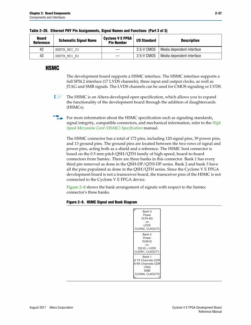
HSMCThe development board supports a HSMC interface. The HSMC interface supports a full SPI4.2 interface (17 LVDS channels), three input and output clocks, as well as JTAG and SMB signals. The LVDS channels can be used for CMOS signaling or LVDS.
1 The HSMC is an Altera-developed open specification, which allows you to expand the functionality of the development board through the addition of daughtercards (HSMCs).
f For more information about the HSMC specification such as signaling standards, signal integrity, compatible connectors, and mechanical information, refer to the High Speed Mezzanine Card (HSMC) Specification manual.
The HSMC connector has a total of 172 pins, including 120 signal pins, 39 power pins, and 13 ground pins. The ground pins are located between the two rows of signal and power pins, acting both as a shield and a reference. The HSMC host connector is based on the 0.5 mm-pitch QSH/QTH family of high-speed, board-to-board connectors from Samtec. There are three banks in this connector. Bank 1 has every third pin removed as done in the QSH-DP/QTH-DP series. Bank 2 and bank 3 have all the pins populated as done in the QSH/QTH series. Since the Cyclone V E FPGA development board is not a transceiver board, the transceiver pins of the HSMC is not connected to the Cyclone V E FPGA device.
Figure 2–8 shows the bank arrangement of signals with respect to the Samtec connector's three banks.
42 ENETB_MDI_P3 — 2.5-V CMOS Media dependent interface
43 ENETB_MDI_N3 — 2.5-V CMOS Media dependent interface
Table 2–20. Ethernet PHY Pin Assignments, Signal Names and Functions (Part 3 of 3)
Board Reference Schematic Signal Name Cyclone V E FPGA
Pin Number I/O Standard Description
Figure 2–8. HSMC Signal and Bank Diagram
Bank 3 Power
D(79.40) -or-
LVDS CLKIN2, CLKOUT2
Bank 2 Power D(39:0)
-or- D[3:0] + LVDS
CLKIN1, CLKOUT1
Bank 18 TX Channels CDR8 RX Channels CDR
JTAGSMB
CLKIN0, CLKOUT0
August 2017 Altera Corporation Cyclone V E FPGA Development BoardReference Manual
2–28 Chapter 2: Board ComponentsComponents and Interfaces
The HSMC interface has programmable bi-directional I/O pins that can be used as 2.5-V LVCMOS, which is 3.3-V LVTTL-compatible. These pins can also be used as various differential I/O standards including, but not limited to, LVDS, mini-LVDS, and RSDS with up to 17 full-duplex channels.
1 As noted in the High Speed Mezzanine Card (HSMC) Specification manual, LVDS and single-ended I/O standards are only guaranteed to function when mixed according to either the generic single-ended pin-out or generic differential pin-out.
Table 2–21 lists the HSMC interface pin assignments, signal names, and functions.
Table 2–21. HSMC Interface Pin Assignments, Schematic Signal Names, and Functions (Part 1 of 3)
Board Reference (J7) Schematic Signal Name
Cyclone V E FPGA Pin Number
I/O Standard Description
33 HSMC_SDA AB22 2.5-V CMOS Management serial data
34 HSMC_SCL AC22 2.5-V CMOS Management serial clock
35 JTAG_TCK AC7 2.5-V CMOS JTAG clock signal
36 HSMC_JTAG_TMS — 2.5-V CMOS JTAG mode select signal
37 HSMC_JTAG_TDO — 2.5-V CMOS JTAG data output
38 JTAC_FPGA_TDO_RETIMER — 2.5-V CMOS JTAG data input
39 HSMC_CLK_OUT0 AJ14 2.5-V CMOS Dedicated CMOS clock out
40 HSMC_CLK_IN0 AB16 2.5-V CMOS Dedicated CMOS clock in
41 HSMC_D0 AH10 2.5-V CMOS Dedicated CMOS I/O bit 0
42 HSMC_D1 AJ10 2.5-V CMOS Dedicated CMOS I/O bit 1
43 HSMC_D2 Y13 2.5-V CMOS Dedicated CMOS I/O bit 2
44 HSMC_D3 AA14 2.5-V CMOS Dedicated CMOS I/O bit 3
47 HSMC_TX_D_P0 AK27 LVDS or 2.5-V LVDS TX bit 0 or CMOS bit 4
48 HSMC_RX_D_P0 Y16 LVDS or 2.5-V LVDS RX bit 0 or CMOS bit 5
49 HSMC_TX_D_N0 AK28 LVDS or 2.5-V LVDS TX bit 0n or CMOS bit 6
50 HSMC_RX_D_N0 AA26 LVDS or 2.5-V LVDS RX bit 0n or CMOS bit 7
53 HSMC_TX_D_P1 AJ27 LVDS or 2.5-V LVDS TX bit 1 or CMOS bit 8
54 HSMC_RX_D_P1 Y17 LVDS or 2.5-V LVDS RX bit 1 or CMOS bit 9
55 HSMC_TX_D_N1 AK26 LVDS or 2.5-V LVDS TX bit 1n or CMOS bit 10
56 HSMC_RX_D_N1 Y18 LVDS or 2.5-V LVDS RX bit 1n or CMOS bit 11
59 HSMC_TX_D_P2 AG26 LVDS or 2.5-V LVDS TX bit 2 or CMOS bit 12
60 HSMC_RX_D_P2 AA18 LVDS or 2.5-V LVDS RX bit 2 or CMOS bit 13
61 HSMC_TX_D_N2 AH26 LVDS or 2.5-V LVDS TX bit 2n or CMOS bit 14
62 HSMC_RX_D_N2 AA19 LVDS or 2.5-V LVDS RX bit 2n or CMOS bit 15
65 HSMC_TX_D_P3 AJ25 LVDS or 2.5-V LVDS TX bit 3 or CMOS bit 16
66 HSMC_RX_D_P3 Y20 LVDS or 2.5-V LVDS RX bit 3 or CMOS bit 17
67 HSMC_TX_D_N3 AK25 LVDS or 2.5-V LVDS TX bit 3n or CMOS bit 18
68 HSMC_RX_D_N3 AA20 LVDS or 2.5-V LVDS RX bit 3n or CMOS bit 19
71 HSMC_TX_D_P4 AH24 LVDS or 2.5-V LVDS TX bit 4 or CMOS bit 20
Cyclone V E FPGA Development Board August 2017 Altera CorporationReference Manual
Chapter 2: Board Components 2–29Components and Interfaces
72 HSMC_RX_D_P4 AA21 LVDS or 2.5-V LVDS RX bit 4 or CMOS bit 21
73 HSMC_TX_D_N4 AJ24 LVDS or 2.5-V LVDS TX bit 4n or CMOS bit 22
74 HSMC_RX_D_N4 AB21 LVDS or 2.5-V LVDS RX bit 4n or CMOS bit 23
77 HSMC_TX_D_P5 AH21 LVDS or 2.5-V LVDS TX bit 5 or CMOS bit 24
78 HSMC_RX_D_P5 AB19 LVDS or 2.5-V LVDS RX bit 5 or CMOS bit 25
79 HSMC_TX_D_N5 AJ22 LVDS or 2.5-V LVDS TX bit 5n or CMOS bit 26
80 HSMC_RX_D_N5 AC19 LVDS or 2.5-V LVDS RX bit 5n or CMOS bit 27
83 HSMC_TX_D_P6 AJ23 LVDS or 2.5-V LVDS TX bit 6 or CMOS bit 28
84 HSMC_RX_D_P6 AC21 LVDS or 2.5-V LVDS RX bit 6 or CMOS bit 29
85 HSMC_TX_D_N6 AK23 LVDS or 2.5-V LVDS TX bit 6n or CMOS bit 30
86 HSMC_RX_D_N6 AD20 LVDS or 2.5-V LVDS RX bit 6n or CMOS bit 31
89 HSMC_TX_D_P7 AK21 LVDS or 2.5-V LVDS TX bit 7 or CMOS bit 32
90 HSMC_RX_D_P7 AD19 LVDS or 2.5-V LVDS RX bit 7 or CMOS bit 33
91 HSMC_TX_D_N7 AK22 LVDS or 2.5-V LVDS TX bit 7n or CMOS bit 34
92 HSMC_RX_D_N7 AE20 LVDS or 2.5-V LVDS RX bit 7n or CMOS bit 35
95 HSMC_CLK_OUT_P1 AE22 LVDS or 2.5-V LVDS or CMOS clock out 1 or CMOS bit 36
96 HSMC_CLK_IN_P1 AB14 LVDS or 2.5-V LVDS or CMOS clock in 1 or CMOS bit 37
97 HSMC_CLK_OUT_N1 AF23 LVDS or 2.5-V LVDS or CMOS clock out 1 or CMOS bit 38
98 HSMC_CLK_IN_N1 AC14 LVDS or 2.5-V LVDS or CMOS clock in 1 or CMOS bit 39
101 HSMC_TX_D_P8 AJ20 LVDS or 2.5-V LVDS TX bit 8 or CMOS bit 40
102 HSMC_RX_D_P8 AF21 LVDS or 2.5-V LVDS RX bit 8 or CMOS bit 41
103 HSMC_TX_D_N8 AK20 LVDS or 2.5-V LVDS TX bit 8n or CMOS bit 42
104 HSMC_RX_D_N8 AG22 LVDS or 2.5-V LVDS RX bit 8n or CMOS bit 43
107 HSMC_TX_D_P9 AJ19 LVDS or 2.5-V LVDS TX bit 9 or CMOS bit 44
108 HSMC_RX_D_P9 AF20 LVDS or 2.5-V LVDS RX bit 9 or CMOS bit 45
109 HSMC_TX_D_N9 AK18 LVDS or 2.5-V LVDS TX bit 9n or CMOS bit 46
110 HSMC_RX_D_N9 AG21 LVDS or 2.5-V LVDS RX bit 9n or CMOS bit 47
113 HSMC_TX_D_P10 AJ17 LVDS or 2.5-V LVDS TX bit 10 or CMOS bit 48
114 HSMC_RX_D_P10 AF18 LVDS or 2.5-V LVDS RX bit 10 or CMOS bit 49
115 HSMC_TX_D_N10 AJ18 LVDS or 2.5-V LVDS TX bit 10n or CMOS bit 50
116 HSMC_RX_D_N10 AF19 LVDS or 2.5-V LVDS RX bit 10n or CMOS bit 51
119 HSMC_TX_D_P11 AK25 LVDS or 2.5-V LVDS TX bit 11 or CMOS bit 52
120 HSMC_RX_D_P11 AG18 LVDS or 2.5-V LVDS RX bit 11 or CMOS bit 53
121 HSMC_TX_D_N11 AG24 LVDS or 2.5-V LVDS TX bit 11n or CMOS bit 54
122 HSMC_RX_D_N11 AG19 LVDS or 2.5-V LVDS RX bit 11n or CMOS bit 55
125 HSMC_TX_D_P12 AH19 LVDS or 2.5-V LVDS TX bit 12 or CMOS bit 56
126 HSMC_RX_D_P12 AK16 LVDS or 2.5-V LVDS RX bit 12 or CMOS bit 57
127 HSMC_TX_D_N12 AH20 LVDS or 2.5-V LVDS TX bit 12n or CMOS bit 58
Table 2–21. HSMC Interface Pin Assignments, Schematic Signal Names, and Functions (Part 2 of 3)
Board Reference (J7) Schematic Signal Name
Cyclone V E FPGA Pin Number
I/O Standard Description
August 2017 Altera Corporation Cyclone V E FPGA Development BoardReference Manual
2–30 Chapter 2: Board ComponentsComponents and Interfaces
RS-232 Serial UARTA female angled DSUB 9-pin connector along with a supporting RS-232 transceiver provides support for implementing a standard RS-232 serial UART channel on this board. The connector has the same pinouts as a data terminal device and requires only a standard cable (no null modem required for PC interface). A dedicated level-shifting buffer is used to translate between LVTTL and RS-232 levels. Board references D23 and D24 are serial UART LEDs that illuminate to indicate RX and TX activity.
Table 2–24 lists the RS-232 serial UART pin assignments, signal names, and functions. The signal names and types are relative to the Cyclone V E FPGA in terms of I/O setting and direction.
128 HSMC_RX_D_N12 AK17 LVDS or 2.5-V LVDS RX bit 12n or CMOS bit 59
131 HSMC_TX_D_P13 AG17 LVDS or 2.5-V LVDS TX bit 13 or CMOS bit 60
132 HSMC_RX_D_P13 AF16 LVDS or 2.5-V LVDS RX bit 13 or CMOS bit 61
133 HSMC_TX_D_N13 AH17 LVDS or 2.5-V LVDS TX bit 13n or CMOS bit 62
134 HSMC_RX_D_N13 AG16 LVDS or 2.5-V LVDS RX bit 13n or CMOS bit 63
137 HSMC_TX_D_P14 AJ15 LVDS or 2.5-V LVDS TX bit 14 or CMOS bit 64
138 HSMC_RX_D_P14 AE16 LVDS or 2.5-V LVDS RX bit 14 or CMOS bit 65
139 HSMC_TX_D_N14 AK15 LVDS or 2.5-V LVDS TX bit 14n or CMOS bit 66
140 HSMC_RX_D_N14 AF15 LVDS or 2.5-V LVDS RX bit 14n or CMOS bit 67
143 HSMC_TX_D_P15 AH14 LVDS or 2.5-V LVDS TX bit 15 or CMOS bit 68
144 HSMC_RX_D_P15 AD17 LVDS or 2.5-V LVDS RX bit 15 or CMOS bit 69
145 HSMC_TX_D_N15 AH15 LVDS or 2.5-V LVDS TX bit 15n or CMOS bit 70
146 HSMC_RX_D_N15 AE17 LVDS or 2.5-V LVDS RX bit 15n or CMOS bit 71
149 HSMC_TX_D_P16 AE15 LVDS or 2.5-V LVDS TX bit 16 or CMOS bit 72
150 HSMC_RX_D_P16 AD18 LVDS or 2.5-V LVDS RX bit 16 or CMOS bit 73
151 HSMC_TX_D_N16 AF14 LVDS or 2.5-V LVDS TX bit 16n or CMOS bit 74
152 HSMC_RX_D_N16 AE18 LVDS or 2.5-V LVDS RX bit 16n or CMOS bit 75
155 HSMC_CLK_OUT_P2 AG23 LVDS or 2.5-V LVDS or CMOS clock out 2 or CMOS bit 76
156 HSMC_CLK_IN_P2 Y15 LVDS or 2.5-V LVDS or CMOS clock in 2 or CMOS bit 77
157 HSMC_CLK_OUT_N2 AH22 LVDS or 2.5-V LVDS or CMOS clock out 2 or CMOS bit 78
158 HSMC_CLK_IN_N2 AA15 LVDS or 2.5-V LVDS or CMOS clock in 2 or CMOS bit 79
160 HSMC_PRSNTn AK5 2.5-V CMOS HSMC port presence detect
Table 2–21. HSMC Interface Pin Assignments, Schematic Signal Names, and Functions (Part 3 of 3)
Board Reference (J7) Schematic Signal Name
Cyclone V E FPGA Pin Number
I/O Standard Description
Table 2–22. RS-232 Serial UART Schematic Signal Names and Functions
Board Reference (U20)
SchematicSignal Name
Cyclone V E FPGA Pin Number I/O Standard Description
14 UART_TXD AB9 3.3-V Transmit data
15 UART_RTS AH6 3.3-V Request to send
Cyclone V E FPGA Development Board August 2017 Altera CorporationReference Manual
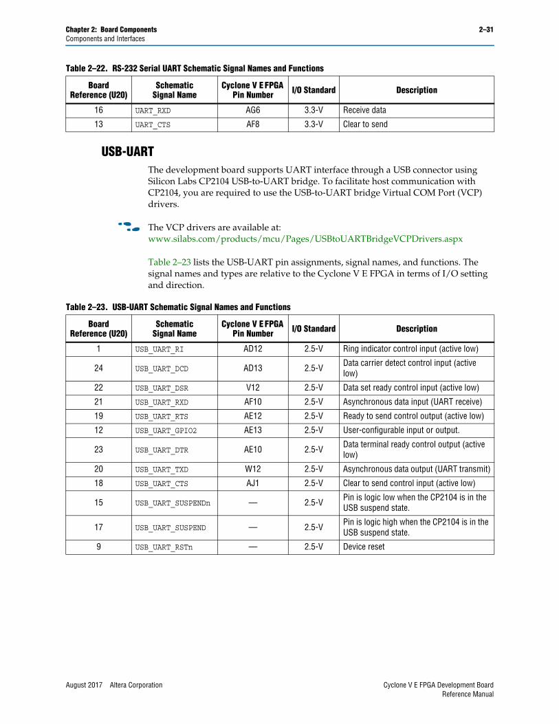
Chapter 2: Board Components 2–31Components and Interfaces
USB-UARTThe development board supports UART interface through a USB connector using Silicon Labs CP2104 USB-to-UART bridge. To facilitate host communication with CP2104, you are required to use the USB-to-UART bridge Virtual COM Port (VCP) drivers.
f The VCP drivers are available at: www.silabs.com/products/mcu/Pages/USBtoUARTBridgeVCPDrivers.aspx
Table 2–23 lists the USB-UART pin assignments, signal names, and functions. The signal names and types are relative to the Cyclone V E FPGA in terms of I/O setting and direction.
16 UART_RXD AG6 3.3-V Receive data
13 UART_CTS AF8 3.3-V Clear to send
Table 2–22. RS-232 Serial UART Schematic Signal Names and Functions
Board Reference (U20)
SchematicSignal Name
Cyclone V E FPGA Pin Number I/O Standard Description
Table 2–23. USB-UART Schematic Signal Names and Functions
Board Reference (U20)
SchematicSignal Name
Cyclone V E FPGA Pin Number I/O Standard Description
1 USB_UART_RI AD12 2.5-V Ring indicator control input (active low)
24 USB_UART_DCD AD13 2.5-V Data carrier detect control input (active low)
22 USB_UART_DSR V12 2.5-V Data set ready control input (active low)
21 USB_UART_RXD AF10 2.5-V Asynchronous data input (UART receive)
19 USB_UART_RTS AE12 2.5-V Ready to send control output (active low)
12 USB_UART_GPIO2 AE13 2.5-V User-configurable input or output.
23 USB_UART_DTR AE10 2.5-V Data terminal ready control output (active low)
20 USB_UART_TXD W12 2.5-V Asynchronous data output (UART transmit)
18 USB_UART_CTS AJ1 2.5-V Clear to send control input (active low)
15 USB_UART_SUSPENDn — 2.5-V Pin is logic low when the CP2104 is in the USB suspend state.
17 USB_UART_SUSPEND — 2.5-V Pin is logic high when the CP2104 is in the USB suspend state.
9 USB_UART_RSTn — 2.5-V Device reset
August 2017 Altera Corporation Cyclone V E FPGA Development BoardReference Manual
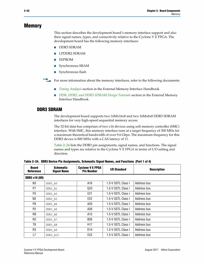
2–32 Chapter 2: Board ComponentsMemory
MemoryThis section describes the development board’s memory interface support and also their signal names, types, and connectivity relative to the Cyclone V E FPGA. The development board has the following memory interfaces:
■ DDR3 SDRAM
■ LPDDR2 SDRAM
■ EEPROM
■ Synchronous SRAM
■ Synchronous flash
f For more information about the memory interfaces, refer to the following documents:
■ Timing Analysis section in the External Memory Interface Handbook.
■ DDR, DDR2, and DDR3 SDRAM Design Tutorials section in the External Memory Interface Handbook.
DDR3 SDRAMThe development board supports two 16Mx16x8 and two 16Mx8x8 DDR3 SDRAM interfaces for very high-speed sequential memory access.
The 32-bit data bus comprises of two x16 devices using soft memory controller (SMC) interface. With SMC, this memory interface runs at a target frequency of 300 MHz for a maximum theoretical bandwidth of over 9.6 Gbps. The maximum frequency for this DDR3 device is 800 MHz with a CAS latency of 11.
Table 2–24 lists the DDR3 pin assignments, signal names, and functions. The signal names and types are relative to the Cyclone V E FPGA in terms of I/O setting and direction.
Table 2–24. DDR3 Device Pin Assignments, Schematic Signal Names, and Functions (Part 1 of 4)
Board Reference
SchematicSignal Name
Cyclone V E FPGAPin Number I/O Standard Description
DDR3 x16 (U8)
N3 DDR3_A0 A16 1.5-V SSTL Class I Address bus
P7 DDR3_A1 G23 1.5-V SSTL Class I Address bus
P3 DDR3_A2 E21 1.5-V SSTL Class I Address bus
N2 DDR3_A3 E22 1.5-V SSTL Class I Address bus
P8 DDR3_A4 A20 1.5-V SSTL Class I Address bus
P2 DDR3_A5 A26 1.5-V SSTL Class I Address bus
R8 DDR3_A6 A15 1.5-V SSTL Class I Address bus
R2 DDR3_A7 B26 1.5-V SSTL Class I Address bus
T8 DDR3_A8 H17 1.5-V SSTL Class I Address bus
R3 DDR3_A9 D14 1.5-V SSTL Class I Address bus
L7 DDR3_A10 E23 1.5-V SSTL Class I Address bus
Cyclone V E FPGA Development Board August 2017 Altera CorporationReference Manual
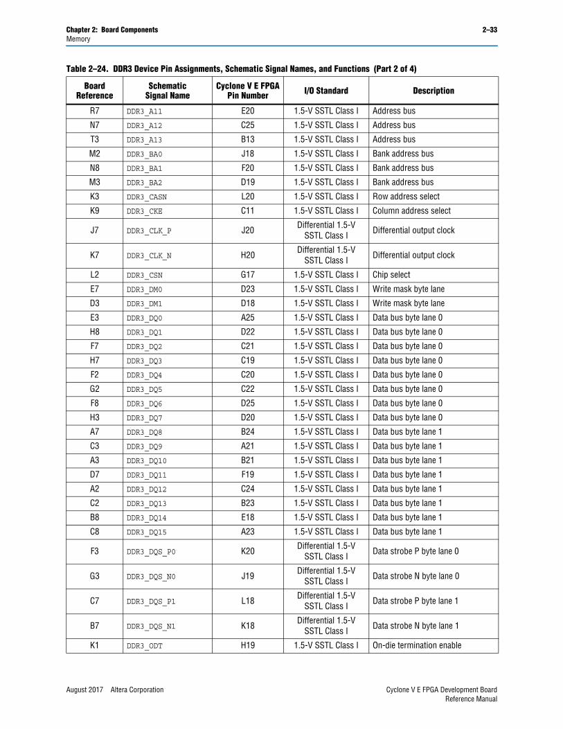
Chapter 2: Board Components 2–33Memory
R7 DDR3_A11 E20 1.5-V SSTL Class I Address bus
N7 DDR3_A12 C25 1.5-V SSTL Class I Address bus
T3 DDR3_A13 B13 1.5-V SSTL Class I Address bus
M2 DDR3_BA0 J18 1.5-V SSTL Class I Bank address bus
N8 DDR3_BA1 F20 1.5-V SSTL Class I Bank address bus
M3 DDR3_BA2 D19 1.5-V SSTL Class I Bank address bus
K3 DDR3_CASN L20 1.5-V SSTL Class I Row address select
K9 DDR3_CKE C11 1.5-V SSTL Class I Column address select
J7 DDR3_CLK_P J20 Differential 1.5-V SSTL Class I Differential output clock
K7 DDR3_CLK_N H20 Differential 1.5-V SSTL Class I Differential output clock
L2 DDR3_CSN G17 1.5-V SSTL Class I Chip select
E7 DDR3_DM0 D23 1.5-V SSTL Class I Write mask byte lane
D3 DDR3_DM1 D18 1.5-V SSTL Class I Write mask byte lane
E3 DDR3_DQ0 A25 1.5-V SSTL Class I Data bus byte lane 0
H8 DDR3_DQ1 D22 1.5-V SSTL Class I Data bus byte lane 0
F7 DDR3_DQ2 C21 1.5-V SSTL Class I Data bus byte lane 0
H7 DDR3_DQ3 C19 1.5-V SSTL Class I Data bus byte lane 0
F2 DDR3_DQ4 C20 1.5-V SSTL Class I Data bus byte lane 0
G2 DDR3_DQ5 C22 1.5-V SSTL Class I Data bus byte lane 0
F8 DDR3_DQ6 D25 1.5-V SSTL Class I Data bus byte lane 0
H3 DDR3_DQ7 D20 1.5-V SSTL Class I Data bus byte lane 0
A7 DDR3_DQ8 B24 1.5-V SSTL Class I Data bus byte lane 1
C3 DDR3_DQ9 A21 1.5-V SSTL Class I Data bus byte lane 1
A3 DDR3_DQ10 B21 1.5-V SSTL Class I Data bus byte lane 1
D7 DDR3_DQ11 F19 1.5-V SSTL Class I Data bus byte lane 1
A2 DDR3_DQ12 C24 1.5-V SSTL Class I Data bus byte lane 1
C2 DDR3_DQ13 B23 1.5-V SSTL Class I Data bus byte lane 1
B8 DDR3_DQ14 E18 1.5-V SSTL Class I Data bus byte lane 1
C8 DDR3_DQ15 A23 1.5-V SSTL Class I Data bus byte lane 1
F3 DDR3_DQS_P0 K20 Differential 1.5-V SSTL Class I Data strobe P byte lane 0
G3 DDR3_DQS_N0 J19 Differential 1.5-V SSTL Class I Data strobe N byte lane 0
C7 DDR3_DQS_P1 L18 Differential 1.5-V SSTL Class I Data strobe P byte lane 1
B7 DDR3_DQS_N1 K18 Differential 1.5-V SSTL Class I Data strobe N byte lane 1
K1 DDR3_ODT H19 1.5-V SSTL Class I On-die termination enable
Table 2–24. DDR3 Device Pin Assignments, Schematic Signal Names, and Functions (Part 2 of 4)
Board Reference
SchematicSignal Name
Cyclone V E FPGAPin Number I/O Standard Description
August 2017 Altera Corporation Cyclone V E FPGA Development BoardReference Manual
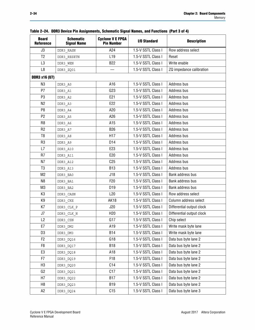
2–34 Chapter 2: Board ComponentsMemory
J3 DDR3_RASN A24 1.5-V SSTL Class I Row address select
T2 DDR3_RESETN L19 1.5-V SSTL Class I Reset
L3 DDR3_WEN B22 1.5-V SSTL Class I Write enable
L8 DDR3_ZQ01 — 1.5-V SSTL Class I ZQ impedance calibration
DDR3 x16 (U7)
N3 DDR3_A0 A16 1.5-V SSTL Class I Address bus
P7 DDR3_A1 G23 1.5-V SSTL Class I Address bus
P3 DDR3_A2 E21 1.5-V SSTL Class I Address bus
N2 DDR3_A3 E22 1.5-V SSTL Class I Address bus
P8 DDR3_A4 A20 1.5-V SSTL Class I Address bus
P2 DDR3_A5 A26 1.5-V SSTL Class I Address bus
R8 DDR3_A6 A15 1.5-V SSTL Class I Address bus
R2 DDR3_A7 B26 1.5-V SSTL Class I Address bus
T8 DDR3_A8 H17 1.5-V SSTL Class I Address bus
R3 DDR3_A9 D14 1.5-V SSTL Class I Address bus
L7 DDR3_A10 E23 1.5-V SSTL Class I Address bus
R7 DDR3_A11 E20 1.5-V SSTL Class I Address bus
N7 DDR3_A12 C25 1.5-V SSTL Class I Address bus
T3 DDR3_A13 B13 1.5-V SSTL Class I Address bus
M2 DDR3_BA0 J18 1.5-V SSTL Class I Bank address bus
N8 DDR3_BA1 F20 1.5-V SSTL Class I Bank address bus
M3 DDR3_BA2 D19 1.5-V SSTL Class I Bank address bus
K3 DDR3_CASN L20 1.5-V SSTL Class I Row address select
K9 DDR3_CKE AK18 1.5-V SSTL Class I Column address select
K7 DDR3_CLK_P J20 1.5-V SSTL Class I Differential output clock
J7 DDR3_CLK_N H20 1.5-V SSTL Class I Differential output clock
L2 DDR3_CSN G17 1.5-V SSTL Class I Chip select
E7 DDR3_DM2 A19 1.5-V SSTL Class I Write mask byte lane
D3 DDR3_DM3 B14 1.5-V SSTL Class I Write mask byte lane
F2 DDR3_DQ16 G18 1.5-V SSTL Class I Data bus byte lane 2
F8 DDR3_DQ17 B18 1.5-V SSTL Class I Data bus byte lane 2
E3 DDR3_DQ18 A18 1.5-V SSTL Class I Data bus byte lane 2
F7 DDR3_DQ19 F18 1.5-V SSTL Class I Data bus byte lane 2
H3 DDR3_DQ20 C14 1.5-V SSTL Class I Data bus byte lane 2
G2 DDR3_DQ21 C17 1.5-V SSTL Class I Data bus byte lane 2
H7 DDR3_DQ22 B17 1.5-V SSTL Class I Data bus byte lane 2
H8 DDR3_DQ23 B19 1.5-V SSTL Class I Data bus byte lane 2
A2 DDR3_DQ24 C15 1.5-V SSTL Class I Data bus byte lane 3
Table 2–24. DDR3 Device Pin Assignments, Schematic Signal Names, and Functions (Part 3 of 4)
Board Reference
SchematicSignal Name
Cyclone V E FPGAPin Number I/O Standard Description
Cyclone V E FPGA Development Board August 2017 Altera CorporationReference Manual
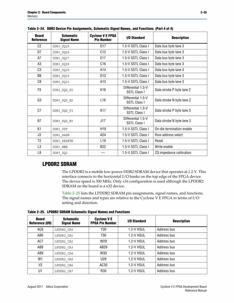
Chapter 2: Board Components 2–35Memory
LPDDR2 SDRAMThe LPDDR2 is a mobile low-power DDR2 SDRAM device that operates at 1.2 V. This interface connects to the horizontal I/O banks on the top edge of the FPGA device. The device speed is 300 MHz. Only x16 configuration is used although the LPDDR2 SDRAM on the board is a x32 device.
Table 2–25 lists the LPDDR2 SDRAM pin assignments, signal names, and functions. The signal names and types are relative to the Cyclone V E FPGA in terms of I/O setting and direction.
C2 DDR3_DQ25 D17 1.5-V SSTL Class I Data bus byte lane 3
D7 DDR3_DQ26 C12 1.5-V SSTL Class I Data bus byte lane 3
A7 DDR3_DQ27 E17 1.5-V SSTL Class I Data bus byte lane 3
A3 DDR3_DQ28 C16 1.5-V SSTL Class I Data bus byte lane 3
C3 DDR3_DQ29 A14 1.5-V SSTL Class I Data bus byte lane 3
B8 DDR3_DQ30 D12 1.5-V SSTL Class I Data bus byte lane 3
C8 DDR3_DQ31 A13 1.5-V SSTL Class I Data bus byte lane 3
F3 DDR3_DQS_P2 K16 Differential 1.5-V SSTL Class I Data strobe P byte lane 2
G3 DDR3_DQS_N2 L16 Differential 1.5-V SSTL Class I Data strobe N byte lane 2
C7 DDR3_DQS_P3 K17 Differential 1.5-V SSTL Class I Data strobe P byte lane 3
B7 DDR3_DQS_N3 J17 Differential 1.5-V SSTL Class I Data strobe N byte lane 3
K1 DDR3_ODT H19 1.5-V SSTL Class I On-die termination enable
J3 DDR3_RASN A24 1.5-V SSTL Class I Row address select
T2 DDR3_RESETN L19 1.5-V SSTL Class I Reset
L3 DDR3_WEN B22 1.5-V SSTL Class I Write enable
L8 DDR3_ZQ2 — 1.5-V SSTL Class I ZQ impedance calibration
Table 2–24. DDR3 Device Pin Assignments, Schematic Signal Names, and Functions (Part 4 of 4)
Board Reference
SchematicSignal Name
Cyclone V E FPGAPin Number I/O Standard Description
Table 2–25. LPDDR2 SDRAM Schematic Signal Names and Functions
Board Reference (U9)
SchematicSignal Name
Cyclone V E FPGA Pin Number I/O Standard Description
AC6 LPDDR2_CA0 Y30 1.2-V HSUL Address bus
AB6 LPDDR2_CA1 T30 1.2-V HSUL Address bus
AC7 LPDDR2_CA2 W29 1.2-V HSUL Address bus
AB8 LPDDR2_CA3 AB29 1.2-V HSUL Address bus
AB9 LPDDR2_CA4 W30 1.2-V HSUL Address bus
W1 LPDDR2_CA5 U29 1.2-V HSUL Address bus
V2 LPDDR2_CA6 AC30 1.2-V HSUL Address bus
U1 LPDDR2_CA7 R30 1.2-V HSUL Address bus
August 2017 Altera Corporation Cyclone V E FPGA Development BoardReference Manual
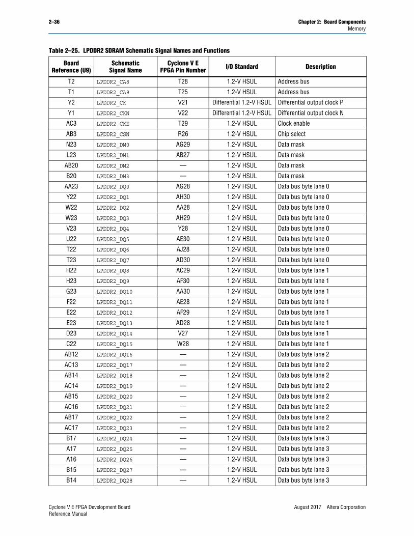
2–36 Chapter 2: Board ComponentsMemory
T2 LPDDR2_CA8 T28 1.2-V HSUL Address bus
T1 LPDDR2_CA9 T25 1.2-V HSUL Address bus
Y2 LPDDR2_CK V21 Differential 1.2-V HSUL Differential output clock P
Y1 LPDDR2_CKN V22 Differential 1.2-V HSUL Differential output clock N
AC3 LPDDR2_CKE T29 1.2-V HSUL Clock enable
AB3 LPDDR2_CSN R26 1.2-V HSUL Chip select
N23 LPDDR2_DM0 AG29 1.2-V HSUL Data mask
L23 LPDDR2_DM1 AB27 1.2-V HSUL Data mask
AB20 LPDDR2_DM2 — 1.2-V HSUL Data mask
B20 LPDDR2_DM3 — 1.2-V HSUL Data mask
AA23 LPDDR2_DQ0 AG28 1.2-V HSUL Data bus byte lane 0
Y22 LPDDR2_DQ1 AH30 1.2-V HSUL Data bus byte lane 0
W22 LPDDR2_DQ2 AA28 1.2-V HSUL Data bus byte lane 0
W23 LPDDR2_DQ3 AH29 1.2-V HSUL Data bus byte lane 0
V23 LPDDR2_DQ4 Y28 1.2-V HSUL Data bus byte lane 0
U22 LPDDR2_DQ5 AE30 1.2-V HSUL Data bus byte lane 0
T22 LPDDR2_DQ6 AJ28 1.2-V HSUL Data bus byte lane 0
T23 LPDDR2_DQ7 AD30 1.2-V HSUL Data bus byte lane 0
H22 LPDDR2_DQ8 AC29 1.2-V HSUL Data bus byte lane 1
H23 LPDDR2_DQ9 AF30 1.2-V HSUL Data bus byte lane 1
G23 LPDDR2_DQ10 AA30 1.2-V HSUL Data bus byte lane 1
F22 LPDDR2_DQ11 AE28 1.2-V HSUL Data bus byte lane 1
E22 LPDDR2_DQ12 AF29 1.2-V HSUL Data bus byte lane 1
E23 LPDDR2_DQ13 AD28 1.2-V HSUL Data bus byte lane 1
D23 LPDDR2_DQ14 V27 1.2-V HSUL Data bus byte lane 1
C22 LPDDR2_DQ15 W28 1.2-V HSUL Data bus byte lane 1
AB12 LPDDR2_DQ16 — 1.2-V HSUL Data bus byte lane 2
AC13 LPDDR2_DQ17 — 1.2-V HSUL Data bus byte lane 2
AB14 LPDDR2_DQ18 — 1.2-V HSUL Data bus byte lane 2
AC14 LPDDR2_DQ19 — 1.2-V HSUL Data bus byte lane 2
AB15 LPDDR2_DQ20 — 1.2-V HSUL Data bus byte lane 2
AC16 LPDDR2_DQ21 — 1.2-V HSUL Data bus byte lane 2
AB17 LPDDR2_DQ22 — 1.2-V HSUL Data bus byte lane 2
AC17 LPDDR2_DQ23 — 1.2-V HSUL Data bus byte lane 2
B17 LPDDR2_DQ24 — 1.2-V HSUL Data bus byte lane 3
A17 LPDDR2_DQ25 — 1.2-V HSUL Data bus byte lane 3
A16 LPDDR2_DQ26 — 1.2-V HSUL Data bus byte lane 3
B15 LPDDR2_DQ27 — 1.2-V HSUL Data bus byte lane 3
B14 LPDDR2_DQ28 — 1.2-V HSUL Data bus byte lane 3
Table 2–25. LPDDR2 SDRAM Schematic Signal Names and Functions
Board Reference (U9)
SchematicSignal Name
Cyclone V E FPGA Pin Number I/O Standard Description
Cyclone V E FPGA Development Board August 2017 Altera CorporationReference Manual
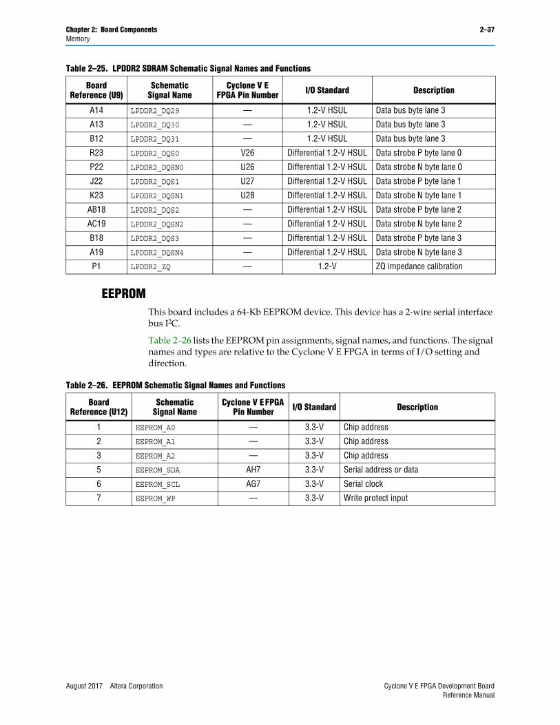
Chapter 2: Board Components 2–37Memory
EEPROMThis board includes a 64-Kb EEPROM device. This device has a 2-wire serial interface bus I2C.
Table 2–26 lists the EEPROM pin assignments, signal names, and functions. The signal names and types are relative to the Cyclone V E FPGA in terms of I/O setting and direction.
A14 LPDDR2_DQ29 — 1.2-V HSUL Data bus byte lane 3
A13 LPDDR2_DQ30 — 1.2-V HSUL Data bus byte lane 3
B12 LPDDR2_DQ31 — 1.2-V HSUL Data bus byte lane 3
R23 LPDDR2_DQS0 V26 Differential 1.2-V HSUL Data strobe P byte lane 0
P22 LPDDR2_DQSN0 U26 Differential 1.2-V HSUL Data strobe N byte lane 0
J22 LPDDR2_DQS1 U27 Differential 1.2-V HSUL Data strobe P byte lane 1
K23 LPDDR2_DQSN1 U28 Differential 1.2-V HSUL Data strobe N byte lane 1
AB18 LPDDR2_DQS2 — Differential 1.2-V HSUL Data strobe P byte lane 2
AC19 LPDDR2_DQSN2 — Differential 1.2-V HSUL Data strobe N byte lane 2
B18 LPDDR2_DQS3 — Differential 1.2-V HSUL Data strobe P byte lane 3
A19 LPDDR2_DQSN4 — Differential 1.2-V HSUL Data strobe N byte lane 3
P1 LPDDR2_ZQ — 1.2-V ZQ impedance calibration
Table 2–25. LPDDR2 SDRAM Schematic Signal Names and Functions
Board Reference (U9)
SchematicSignal Name
Cyclone V E FPGA Pin Number I/O Standard Description
Table 2–26. EEPROM Schematic Signal Names and Functions
Board Reference (U12)
SchematicSignal Name
Cyclone V E FPGA Pin Number I/O Standard Description
1 EEPROM_A0 — 3.3-V Chip address
2 EEPROM_A1 — 3.3-V Chip address
3 EEPROM_A2 — 3.3-V Chip address
5 EEPROM_SDA AH7 3.3-V Serial address or data
6 EEPROM_SCL AG7 3.3-V Serial clock
7 EEPROM_WP — 3.3-V Write protect input
August 2017 Altera Corporation Cyclone V E FPGA Development BoardReference Manual
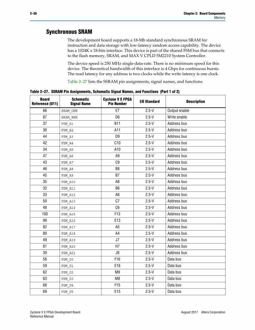
2–38 Chapter 2: Board ComponentsMemory
Synchronous SRAMThe development board supports a 18-Mb standard synchronous SRAM for instruction and data storage with low-latency random access capability. The device has a 1024K x 18-bits interface. This device is part of the shared FSM bus that connects to the flash memory, SRAM, and MAX V CPLD 5M2210 System Controller.
The device speed is 250 MHz single-data-rate. There is no minimum speed for this device. The theoretical bandwidth of this interface is 4 Gbps for continuous bursts. The read latency for any address is two clocks while the write latency is one clock.
Table 2–27 lists the SSRAM pin assignments, signal names, and functions.
Table 2–27. SSRAM Pin Assignments, Schematic Signal Names, and Functions (Part 1 of 2)
Board Reference (U11)
SchematicSignal Name
Cyclone V E FPGAPin Number I/O Standard Description
86 SRAM_OEN E7 2.5-V Output enable
87 SRAM_WEN D6 2.5-V Write enable
37 FSM_A1 B11 2.5-V Address bus
36 FSM_A2 A11 2.5-V Address bus
44 FSM_A3 D9 2.5-V Address bus
42 FSM_A4 C10 2.5-V Address bus
34 FSM_A5 A10 2.5-V Address bus
47 FSM_A6 A9 2.5-V Address bus
43 FSM_A7 C9 2.5-V Address bus
46 FSM_A8 B8 2.5-V Address bus
45 FSM_A9 B7 2.5-V Address bus
35 FSM_A10 A8 2.5-V Address bus
32 FSM_A11 B6 2.5-V Address bus
33 FSM_A12 A6 2.5-V Address bus
50 FSM_A13 C7 2.5-V Address bus
48 FSM_A14 C6 2.5-V Address bus
100 FSM_A15 F13 2.5-V Address bus
99 FSM_A16 E13 2.5-V Address bus
82 FSM_A17 A5 2.5-V Address bus
80 FSM_A18 A4 2.5-V Address bus
49 FSM_A19 J7 2.5-V Address bus
81 FSM_A20 H7 2.5-V Address bus
39 FSM_A21 J9 2.5-V Address bus
58 FSM_D0 F16 2.5-V Data bus
59 FSM_D1 E16 2.5-V Data bus
62 FSM_D2 M9 2.5-V Data bus
63 FSM_D3 M8 2.5-V Data bus
68 FSM_D4 F15 2.5-V Data bus
69 FSM_D5 E15 2.5-V Data bus
Cyclone V E FPGA Development Board August 2017 Altera CorporationReference Manual
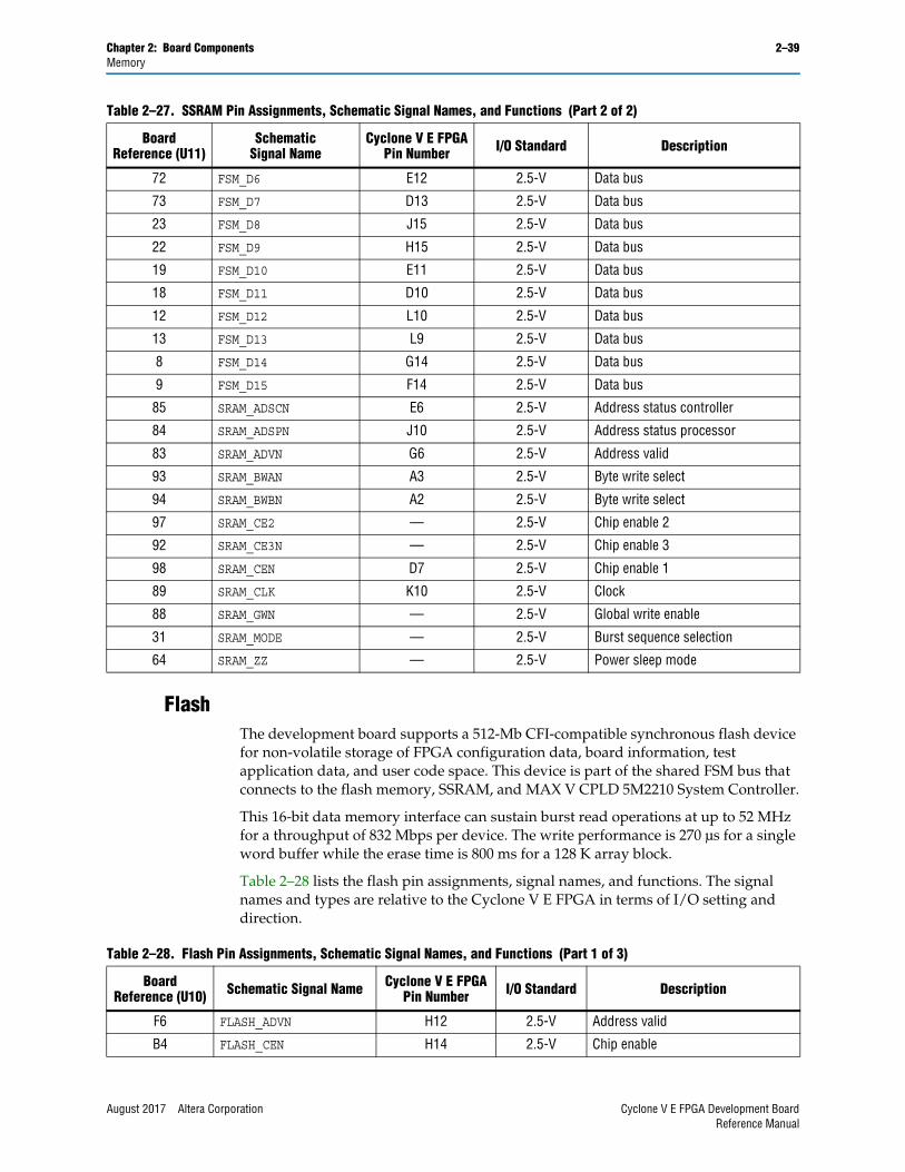
Chapter 2: Board Components 2–39Memory
FlashThe development board supports a 512-Mb CFI-compatible synchronous flash device for non-volatile storage of FPGA configuration data, board information, test application data, and user code space. This device is part of the shared FSM bus that connects to the flash memory, SSRAM, and MAX V CPLD 5M2210 System Controller.
This 16-bit data memory interface can sustain burst read operations at up to 52 MHz for a throughput of 832 Mbps per device. The write performance is 270 µs for a single word buffer while the erase time is 800 ms for a 128 K array block.
Table 2–28 lists the flash pin assignments, signal names, and functions. The signal names and types are relative to the Cyclone V E FPGA in terms of I/O setting and direction.
72 FSM_D6 E12 2.5-V Data bus
73 FSM_D7 D13 2.5-V Data bus
23 FSM_D8 J15 2.5-V Data bus
22 FSM_D9 H15 2.5-V Data bus
19 FSM_D10 E11 2.5-V Data bus
18 FSM_D11 D10 2.5-V Data bus
12 FSM_D12 L10 2.5-V Data bus
13 FSM_D13 L9 2.5-V Data bus
8 FSM_D14 G14 2.5-V Data bus
9 FSM_D15 F14 2.5-V Data bus
85 SRAM_ADSCN E6 2.5-V Address status controller
84 SRAM_ADSPN J10 2.5-V Address status processor
83 SRAM_ADVN G6 2.5-V Address valid
93 SRAM_BWAN A3 2.5-V Byte write select
94 SRAM_BWBN A2 2.5-V Byte write select
97 SRAM_CE2 — 2.5-V Chip enable 2
92 SRAM_CE3N — 2.5-V Chip enable 3
98 SRAM_CEN D7 2.5-V Chip enable 1
89 SRAM_CLK K10 2.5-V Clock
88 SRAM_GWN — 2.5-V Global write enable
31 SRAM_MODE — 2.5-V Burst sequence selection
64 SRAM_ZZ — 2.5-V Power sleep mode
Table 2–27. SSRAM Pin Assignments, Schematic Signal Names, and Functions (Part 2 of 2)
Board Reference (U11)
SchematicSignal Name
Cyclone V E FPGAPin Number I/O Standard Description
Table 2–28. Flash Pin Assignments, Schematic Signal Names, and Functions (Part 1 of 3)
Board Reference (U10) Schematic Signal Name Cyclone V E FPGA
Pin Number I/O Standard Description
F6 FLASH_ADVN H12 2.5-V Address valid
B4 FLASH_CEN H14 2.5-V Chip enable
August 2017 Altera Corporation Cyclone V E FPGA Development BoardReference Manual
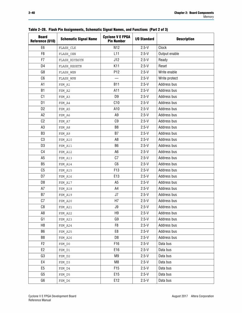
2–40 Chapter 2: Board ComponentsMemory
E6 FLASH_CLK N12 2.5-V Clock
F8 FLASH_OEN L11 2.5-V Output enable
F7 FLASH_RDYBSYN J12 2.5-V Ready
D4 FLASH_RESETN K11 2.5-V Reset
G8 FLASH_WEN P12 2.5-V Write enable
C6 FLASH_WPN — 2.5-V Write protect
A1 FSM_A1 B11 2.5-V Address bus
B1 FSM_A2 A11 2.5-V Address bus
C1 FSM_A3 D9 2.5-V Address bus
D1 FSM_A4 C10 2.5-V Address bus
D2 FSM_A5 A10 2.5-V Address bus
A2 FSM_A6 A9 2.5-V Address bus
C2 FSM_A7 C9 2.5-V Address bus
A3 FSM_A8 B8 2.5-V Address bus
B3 FSM_A9 B7 2.5-V Address bus
C3 FSM_A10 A8 2.5-V Address bus
D3 FSM_A11 B6 2.5-V Address bus
C4 FSM_A12 A6 2.5-V Address bus
A5 FSM_A13 C7 2.5-V Address bus
B5 FSM_A14 C6 2.5-V Address bus
C5 FSM_A15 F13 2.5-V Address bus
D7 FSM_A16 E13 2.5-V Address bus
D8 FSM_A17 A5 2.5-V Address bus
A7 FSM_A18 A4 2.5-V Address bus
B7 FSM_A19 J7 2.5-V Address bus
C7 FSM_A20 H7 2.5-V Address bus
C8 FSM_A21 J9 2.5-V Address bus
A8 FSM_A22 H9 2.5-V Address bus
G1 FSM_A23 G9 2.5-V Address bus
H8 FSM_A24 F8 2.5-V Address bus
B6 FSM_A25 E8 2.5-V Address bus
B8 FSM_A26 D8 2.5-V Address bus
F2 FSM_D0 F16 2.5-V Data bus
E2 FSM_D1 E16 2.5-V Data bus
G3 FSM_D2 M9 2.5-V Data bus
E4 FSM_D3 M8 2.5-V Data bus
E5 FSM_D4 F15 2.5-V Data bus
G5 FSM_D5 E15 2.5-V Data bus
G6 FSM_D6 E12 2.5-V Data bus
Table 2–28. Flash Pin Assignments, Schematic Signal Names, and Functions (Part 2 of 3)
Board Reference (U10) Schematic Signal Name Cyclone V E FPGA
Pin Number I/O Standard Description
Cyclone V E FPGA Development Board August 2017 Altera CorporationReference Manual
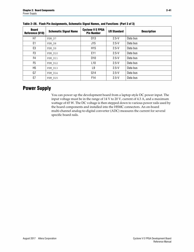
Chapter 2: Board Components 2–41Power Supply
Power SupplyYou can power up the development board from a laptop-style DC power input. The input voltage must be in the range of 14 V to 20 V, current of 4.3 A, and a maximum wattage of 65 W. The DC voltage is then stepped down to various power rails used by the board components and installed into the HSMC connectors. An on-board multi-channel analog-to-digital converter (ADC) measures the current for several specific board rails.
H7 FSM_D7 D13 2.5-V Data bus
E1 FSM_D8 J15 2.5-V Data bus
E3 FSM_D9 H15 2.5-V Data bus
F3 FSM_D10 E11 2.5-V Data bus
F4 FSM_D11 D10 2.5-V Data bus
F5 FSM_D12 L10 2.5-V Data bus
H5 FSM_D13 L9 2.5-V Data bus
G7 FSM_D14 G14 2.5-V Data bus
E7 FSM_D15 F14 2.5-V Data bus
Table 2–28. Flash Pin Assignments, Schematic Signal Names, and Functions (Part 3 of 3)
Board Reference (U10) Schematic Signal Name Cyclone V E FPGA
Pin Number I/O Standard Description
August 2017 Altera Corporation Cyclone V E FPGA Development BoardReference Manual
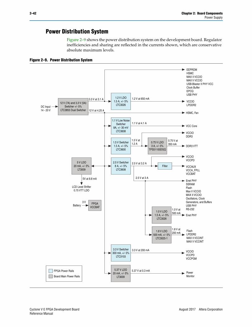
2–42 Chapter 2: Board ComponentsPower Supply
Power Distribution SystemFigure 2–9 shows the power distribution system on the development board. Regulator inefficiencies and sharing are reflected in the currents shown, which are conservative absolute maximum levels.
Figure 2–9. Power Distribution System
1.2 V LDO1.5 A, +/- 5%
LTC3026
HSMC, Fan
EEPROMHSMCMAX II VCCIOMAX V VCCIOUSB-Blaster II PHY VCCClock BufferEPCQUSB PHY
Battery3 V
5.37 V LDO20 mA, +/- 5%
LT3009
5.37 V at 0.3 mAPowerMonitor
1.0 V LDO1.5 A, +/- 5%
LTC3026
1.0 V at500 mA
1.8 V LDO500 mA, +/- 5%
LTC3025-1
1.8 V at200 mA
Enet PHY
FlashLPDDR2MAX II VCCINTMAX V VCCINT
Enet PHYSSRAMFlashMax V VCCIOMAX II VCCIOOscillators, ClockGenerators, and BuffersUSB PHYRS-232
Filter
VCC Core
VCCIOLPDDR2
3.3 V at 3.1 A
12 V at 4.25 ADC Input14 - 20 V
FPGA Power Rails
Board Main Power Rails
1.2 V at 650 mA
1.1 V Low NoiseSwitcher
8A, +/- 30 mVLTC3608
1.1 V at 4.1 A
1.5 V Switcher1.5 A, +/- 5%
LTC3600
1.5 V at 1.2 A
2.5 V Switcher8 A, +/- 5%LTC3608
2.5 V at 3.2 A
3.3 V Switcher300 mA, +/- 5%
LTC3103
2.5 V at 3 A
3.3 V at 200 mA VCCIOVCCPDVCCPGM
LCD Level Shifter0.75 VTT LDO
5V at 8.8 mA
12 V (7A) and 3.3 V (5A)Switcher +/- 5%
LTC3855 Dual Switcher
5 V LDO20 mA, +/- 5%
LT3009
FPGAVCCBAT
VCCIOVCCPD
VCCAUXVCCA_FPLLVCCBAT
0.75 V LDO3 A, +/- 5%
TPS51100DGQ
0.75 V at350 mA
DDR3 VTT
VCCIODDR3
Cyclone V E FPGA Development Board August 2017 Altera CorporationReference Manual
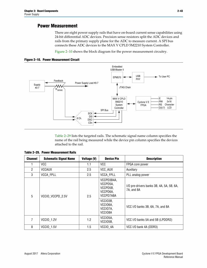
Chapter 2: Board Components 2–43Power Supply
Power MeasurementThere are eight power supply rails that have on-board current sense capabilities using 24-bit differential ADC devices. Precision sense resistors split the ADC devices and rails from the primary supply plane for the ADC to measure current. A SPI bus connects these ADC devices to the MAX V CPLD 5M2210 System Controller.
Figure 2–10 shows the block diagram for the power measurement circuitry.
Table 2–29 lists the targeted rails. The schematic signal name column specifies the name of the rail being measured while the device pin column specifies the devices attached to the rail.
Figure 2–10. Power Measurement Circuit
SCKSPI Bus
DSIDSOCSn
8 Ch.
Power Supply Load #0-7
R SENSE
MAX V CPLD5M2210System
Controller
Cyclone V EFPGA
To User PC
JTAG Chain
Feedback
14-pin2x16
CharacterLCD
ERWRSD(0:7)
Supply#0-7
EPM570 USBPHY
EmbeddedUSB-Blaster II
Table 2–29. Power Measurement Rails
Channel Schematic Signal Name Voltage (V) Device Pin Description
1 VCC 1.1 VCC FPGA core power
2 VCCAUX 2.5 VCC_AUX Auxiliary
3 VCCA_FPLL 2.5 VCCA_FPLL PLL analog power
5 VCCIO_VCCPD_2.5V 2.5
VCCPD3B4A, VCCPD5A, VCCPD5B, VCCPD6A, VCCPD7A8A
I/O pre-drivers banks 3B, 4A, 5A, 5B, 6A, 7A, and 8A
VCCIO3B, VCCIO6A, VCCIO7A, VCCIO8A
VCC I/O banks 3B, 6A, 7A, and 8A
7 VCCIO_1.2V 1.2 VCCIO5A, VCCIO5B, VCC I/O banks 5A and 5B (LPDDR2)
8 VCCIO_1.5V 1.5 VCCIO_4A VCC I/O bank 4A (DDR3)
August 2017 Altera Corporation Cyclone V E FPGA Development BoardReference Manual
2–44 Chapter 2: Board ComponentsPower Supply
Cyclone V E FPGA Development Board August 2017 Altera CorporationReference Manual
August 2017 Altera Corporation
3. Board Components Reference
This chapter describes the Cyclone V E FPGA development board components, the manufacturing information, and the board compliance statements.
Board ComponentsTable lists the component reference and manufacturing information of all the components on the development board.
Table 3–1. Component Reference and Manufacturing Information
Board Reference Component Manufacturer Manufacturing
Part NumberManufacturer
Website
U1 FPGA, Cyclone V E F896, 149,500 LEs, leadfree Altera Corporation 5CEFA7F31I7N www.altera.com
U13 MAX V CPLD 5M2210 System Controller Altera Corporation 5M2210ZF256I5N www.altera.com
U18 High-Speed USB peripheral controller Cypress CY7C68013A www.cypress.com
D1-D16, D18-D31, Green LEDs Lumex Inc. SML-LXT0805GW-TR www.lumex.com
D17 Red LED Lumex Inc. SML-LXT0805IW-TR www.lumex.com
D35 Blue LED Lumex Inc. SML-LX0805USBC-TR www.lumex.com
SW1–SW4 Four-position DIP switches C&K Components/ ITT Industries TDA04H0SB1 www.ittcannon.com
S1-S8 Push buttons Panasonic EVQPAC07K www.panasonic.com
S5 Slide switch E-switch EG2201A www.e-switch.com
X1 Programmable LVDS clock 125M defaults Silicon Labs 570FAB000973DG www.silabs.com
X3 100 MHz crystal oscillator, ±50 ppm, CMOS, 2.5 V Silicon Labs 510GBA100M000BAGx www.silabs.com
X2 50 MHz crystal oscillator, ±50 ppm, CMOS, 2.5 V Silicon Labs 510GBA50M0000BAGx www.silabs.com
J12 Female angled PCB WR-DSUB 9-pin connector Wurth Elektronik 618009231121 www.we-online.com
U21 USB-to-UART bridge Silicon Labs CP2104 www.silabs.com
J142×7 pin LCD socket strip Samtec TSM-107-07-G-D www.samtec.com
2×16 character LCD, 5×8 dot matrix Lumex Inc. LCM-S01602DSR/C www.lumex.com
U14, U15 Ethernet PHY BASE-T devices Marvell Semiconductor
88E1111-B2-CAA1C000 www.marvell.com
J8, J9 RJ-45 connectors, 10/100/1000 Mbps Wurth Elektronik 7499111001A www.we-online.com
J7 HSMC, custom version of QSH-DP family high-speed socket. Samtec ASP-122953-01 www.samtec.com
U20 RS-232 dual transceiver Linear Technology LTC2803-1 www.linear.com
Cyclone V E FPGA Development BoardReference Manual
3–2 Chapter 3: Board Components ReferenceStatement of China-RoHS Compliance
Statement of China-RoHS ComplianceTable 3–2 lists hazardous substances included with the kit.
CE EMI Conformity CautionThis development kit is delivered conforming to relevant standards mandated by Directive 2004/108/EC. Because of the nature of programmable logic devices, it is possible for the user to modify the kit in such a way as to generate electromagnetic interference (EMI) that exceeds the limits established for this equipment. Any EMI caused as the result of modifications to the delivered material is the responsibility of the user.
U12 64-Kb EEPROM Microchip 24AA64 www.microchip.com
J15, J16 2 x 8 debug headers Samtec TSM-108-01-L-DV www.samtec.com
U7, U8 16M × 16 × 8, 256-MB DDR3 SDRAM Micron MT41J128M16 www.micron.com
U9 16M × 32 × 8, 512-MB LPDDR2 SDRAM Micron MT42L128M32 www.micron.com
U11 1024K × 18 bit 18-Mb synchronous SRAM
Integrated Silicon Solution, Inc.
IS61VPS102418A-250TQL www.issi.com
U10 512-Mb synchronous flash Numonyx PC28F512P30BF www.numonyx.com
U35 16-channel differential 24-bit ADC Linear Technology LTC2418CGN#PBF www.linear.com
Table 3–1. Component Reference and Manufacturing Information
Board Reference Component Manufacturer Manufacturing
Part NumberManufacturer
Website
Table 3–2. Table of Hazardous Substances’ Name and Concentration Notes (1), (2)
Part Name Lead (Pb)
Cadmium (Cd)
Hexavalent Chromium
(Cr6+)
Mercury (Hg)
Polybrominatedbiphenyls (PBB)
Polybrominateddiphenyl Ethers
(PBDE)
Cyclone V E development board X* 0 0 0 0 0
15 V power supply 0 0 0 0 0 0
Type A-B USB cable 0 0 0 0 0 0
User guide 0 0 0 0 0 0
Notes to Table 3–2:
(1) 0 indicates that the concentration of the hazardous substance in all homogeneous materials in the parts is below the relevant threshold of the SJ/T11363-2006 standard.
(2) X* indicates that the concentration of the hazardous substance of at least one of all homogeneous materials in the parts is above the relevant threshold of the SJ/T11363-2006 standard, but it is exempted by EU RoHS.
Cyclone V E FPGA Development Board August 2017 Altera CorporationReference Manual
August 2017 Altera Corporation
Additional Information
This chapter provides additional information about the document and Altera.
Board Revision HistoryThe following table lists the versions of all releases of the Cyclone V E FPGA Development Board.
Document Revision HistoryThe following table lists the revision history for this document.
Typographic ConventionsThe following table shows the typographic conventions this document uses.
Release Date Version Description
March 2013 Production silicon■ New board revision. New device part number—5CEFA7F31I7N.
■ Board passed CE compliance testing.
November 2012 Engineering silicon Initial release.
Date Version Changes
August 2017 1.4 Corrected board location for Clock Output SMA Connector in “Overview of the Cyclone V E FPGA Development Board Features” on page 2–2.
January 2017 1.3 Corrected ENETA_RX_DV pin number in Table 2–20 on page 2–25.
September 2015 1.2■ Added link to Altera Design Store in “MAX V CPLD 5M2210 System Controller” on
page 2–5.
■ Corrected device label in Figure 2–5 on page 2–15.
March 2013 1.1■ Revised the FPGA device part number for production silicon release.
■ Added a section about “CE EMI Conformity Caution” on page 3–2.
November 2012 1.0 Initial release.
Visual Cue Meaning
Bold Type with Initial Capital Letters
Indicate command names, dialog box titles, dialog box options, and other GUI labels. For example, Save As dialog box. For GUI elements, capitalization matches the GUI.
bold typeIndicates directory names, project names, disk drive names, file names, file name extensions, software utility names, and GUI labels. For example, \qdesigns directory, D: drive, and chiptrip.gdf file.
Italic Type with Initial Capital Letters Indicate document titles. For example, Stratix IV Design Guidelines.
Cyclone V E FPGA Development BoardReference Manual
Info–2 Additional InformationAdditional InformationTypographic Conventions
italic typeIndicates variables. For example, n + 1.
Variable names are enclosed in angle brackets (< >). For example, <file name> and <project name>.pof file.
Initial Capital Letters Indicate keyboard keys and menu names. For example, the Delete key and the Options menu.
“Subheading Title” Quotation marks indicate references to sections in a document and titles of Quartus II Help topics. For example, “Typographic Conventions.”
Courier type
Indicates signal, port, register, bit, block, and primitive names. For example, data1, tdi, and input. The suffix n denotes an active-low signal. For example, resetn.
Indicates command line commands and anything that must be typed exactly as it appears. For example, c:\qdesigns\tutorial\chiptrip.gdf.
Also indicates sections of an actual file, such as a Report File, references to parts of files (for example, the AHDL keyword SUBDESIGN), and logic function names (for example, TRI).
r An angled arrow instructs you to press the Enter key.
1., 2., 3., anda., b., c., and so on
Numbered steps indicate a list of items when the sequence of the items is important, such as the steps listed in a procedure.
■ ■ ■ Bullets indicate a list of items when the sequence of the items is not important.
1 The hand points to information that requires special attention.
h The question mark directs you to a software help system with related information.
f The feet direct you to another document or website with related information.
m The multimedia icon directs you to a related multimedia presentation.
c A caution calls attention to a condition or possible situation that can damage or destroy the product or your work.
w A warning calls attention to a condition or possible situation that can cause you injury.
The envelope links to the Email Subscription Management Center page of the Altera website, where you can sign up to receive update notifications for Altera documents.
The feedback icon allows you to submit feedback to Altera about the document. Methods for collecting feedback vary as appropriate for each document.
Visual Cue Meaning
Cyclone V E FPGA Development Board August 2017 Altera CorporationReference Manual
Recommended
![Cyclone Handbook, Section I. Cyclone FPGA Family Data Sheet1]EP1C12F256C8.pdf · Section I. Cyclone FPGA Family Data Sheet ... Cyclone Device Handbook, ... Vertical migration means](https://img.pdfslide.us/doc/110x75/5b3a24897f8b9a600a8f2cfc/cyclone-handbook-section-i-cyclone-fpga-family-data-sheet-1ep1c12f256c8pdf.jpg)