PIONEER CORPORATION 4-1, Meguro 1-Chome, Meguro-ku, Tokyo 153-8654, Japan PIONEER ELECTRONICS SERVICE INC. P.O.Box 1760, Long Beach, CA 90801-1760 U.S.A.PIONEER EUROPE NV Haven 1087 Keetberglaan 1, 9120 Melsele, Belgium PIONEER ELECTRONICS ASIACENTRE PTE.LTD. 253 Alexandra Road, #04-01, Singapore 159936
C PIONEER CORPORATION 2000 K-ZZA. OCT. 2000 Printed in Japan
ORDER NO.
CRT2559
HIGH POWER CD PLAYER WITH FM/AM TUNER
DEH-2350 X1M/ES
ServiceManual
CONTENTS
1. SAFETY INFORMATION ............................................2
2. EXPLODED VIEWS AND PARTS LIST .......................2
3. BLOCK DIAGRAM AND SCHEMATIC DIAGRAM .....8
4. PCB CONNECTION DIAGRAM ................................24
5. ELECTRICAL PARTS LIST ........................................32
6. ADJUSTMENT..........................................................35
7. GENERAL INFORMATION .......................................39
7.1 DIAGNOSIS ........................................................39
7.1.1 TEST MODE..............................................39
7.1.2 DISASSEMBLY .........................................42
7.1.3 CONNECTOR FUNCTION DESCRIPTION.......46
7.2 PARTS .................................................................47
7.2.1 IC................................................................47
7.2.2 DISPLAY....................................................54
7.3 OPERATIONAL FLOW CHART...........................55
8. OPERATIONS AND SPECIFICATIONS.....................56
DEH-1350 X1M/ES
DEH-2350/X1M/ES
- This service manual should be used together with the following manual(s):Model No. Order No. Mech. Module Remarks
CX-958 CRT2423 S8.1 CD Mech. Module:Circuit Description, Mech.Description, Disassembly
2
DEH-2350,1350
- CD Player Service Precautions
1. For pickup unit(CXX1285) handling, please refer
to"Disassembly"(see page 42).
During replacement, handling precautions shall be
taken to prevent an electrostatic discharge(protection
by a short pin).
2. During disassembly, be sure to turn the power off
since an internal IC might be destroyed when a con-
nector is plugged or unplugged.
3. Please checking the grating after changing the ser-
vice pickup unit(see page 37).
1. SAFETY INFORMATION
2. EXPLODED VIEWS AND PARTS LIST
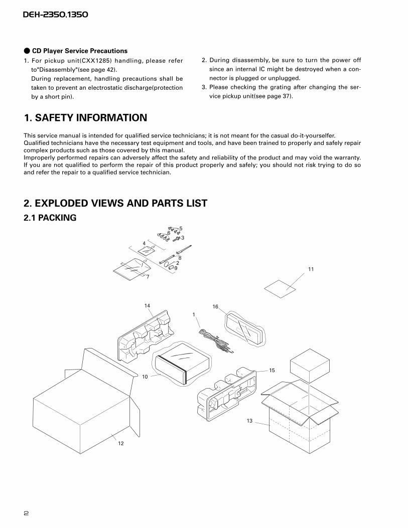
2.1 PACKING
14
1
16
10
12
13
15
11
5
928
7
6
43
This service manual is intended for qualified service technicians; it is not meant for the casual do-it-yourselfer.Qualified technicians have the necessary test equipment and tools, and have been trained to properly and safely repaircomplex products such as those covered by this manual.Improperly performed repairs can adversely affect the safety and reliability of the product and may void the warranty.If you are not qualified to perform the repair of this product properly and safely; you should not risk trying to do soand refer the repair to a qualified service technician.

3
DEH-2350,1350
1 Cord Assy CDE64682 Spring CBH16503 Screw CBA1002
* 4 Polyethylene Bag CEG-1275 Screw CRZ50P090FMC
6 Screw TRZ50P080FMC* 7 Polyethylene Bag CEG-158
8 Handle CNC53959 Bush CNV3930
10 Polyethylene Bag CEG-162
11-1 •••••11-2 Owner’s Manual CRD328111-3 Installation Manual CRD3283
12 Carton See Contrast table(2)13 Contain Box See Contrast table(2)
14 Protector CHP234615 Protector CHP234716 Case Assy See Contrast table(2)
Mark No. Description Part No. Mark No. Description Part No.
(1) PACKING SECTION PARTS LIST
NOTE:
- Parts marked by “*” are generally unavailable because they are not in our Master Spare Parts List.
- Screws adjacent to ∇ mark on the product are used for disassembly.
Part No.Mark No. Symbol and Description DEH-2350/X1M/ES DEH-1350/X1M/ES
12 Carton CHG4150 CHG415713 Contain Box CHL4150 CHL415716 Case Assy CXB3520 Not used
(2) CONTRAST TABLE
DEH-2350/X1M/ES and DEH-1350/X1M/ES are constructed the same except for the following:
- Owner's Manual, Installation ManualModel Part No. Language
DEH-2350/X1M/ES CRD3281 English, Spanish, Portuguese(B),DEH-1350/X1M/ES CRD3283 Chinese, Arabic
4
DEH-2350,1350
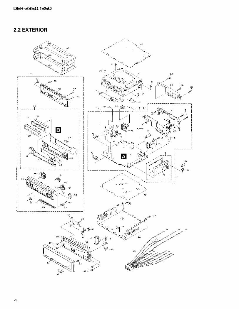
2.2 EXTERIOR
B
A

5
DEH-2350,1350
1 Tuner Amp Unit See Contrast table(2)2 Screw ASZ26P080FMC3 Screw BPZ26P080FMC4 Screw BSZ26P160FMC5 FM/AM Tuner Unit CWE1563
6 Holder CNC88157 Pin Jack(CN301) CKB10418 Terminal(CN403) CKF10599 Plug(CN901) CKM1330
10 Connector(CN601) CKS3581
11 Connector(CN605) CKS383812 Antenna Jack(CN402) CKX105613 Holder CNC804114 Holder CNC804315 Holder CNC9128
16 Heat Sink CNR158917 Button CAC483618 Spring CBH183519 Spring CBH220820 •••••
21 Screw BSZ26P060FMC22 Screw BSZ30P060FMC23 Screw BSZ30P120FMC24 Cable CDE616025 Cord Assy CDE6468
26 Fuse(10A) CEK113627 CD Mechanism Module(S8.1) CXK520328 Holder CNC570429 Cover CNC912730 Cushion CNM5210
31 Insulator CNM622432 Insulator CNM638633 Panel CNS634434 Spring CBH236735 Bracket CNC6791
36 Holder CNC804237 Cover CNM627638 Panel CNS535539 Arm CNV469240 Arm CNV4728
41 Arm CNV557642 Screw IMS20P030FZK43 Case Unit CXB403344 Chassis Unit CXB462545 Detach Grille Assy See Contrast table(2)
46 Screw BPZ20P100FZK47 Button(DETACH) CAC578948 Button(+/-, EQ, LD) CAC682149 Button(1-6, CLK) CAC682250 Button(A, B) CAC6823
51 Button(EJECT/BSM) CAC682452 Button(CROSS) CAC682553 Button(SOURCE) CAC685154 Spring CBH221055 Cover CNS6114
56 Keyboard Unit See Contrast table(2)57 LCD See Contrast table(2)58 Connector(CN1801) CKS358059 Holder CNC907860 Sheet CNM7057
61 Lighting Conductor CNV647562 Lighting Conductor CNV647663 Rubber CNV647764 Rubber CNV647865 Grille Unit See Contrast table(2)
66 Holder Unit CXB668167 Screw ISS26P055FUC68 IC(IC302) PAL006A69 Transistor(Q904, 981) 2SD2396
(1) EXTERIOR SECTION PARTS LIST
Mark No. Description Part No. Mark No. Description Part No.
Part No.Mark No. Symbol and Description DEH-2350/X1M/ES DEH-1350/X1M/ES
1 Tuner Amp Unit CWM7293 CWM729745 Detach Grille Assy CXB6146 CXB615056 Keyboard Unit CWM7303 CWM730757 LCD CAW1606 CAW163365 Grille Unit CXB7182 CXB7186
(2) CONTRAST TABLE
DEH-2350/X1M/ES and DEH-1350/X1M/ES are constructed the same except for the following:

6
DEH-2350,1350
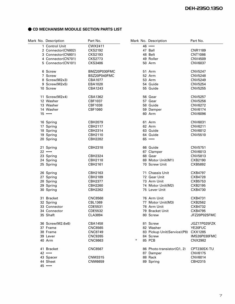
2.3 CD MECHANISM MODULE
C
D
7
DEH-2350,1350
Mark No. Description Part No. Mark No. Description Part No.
1 Control Unit CWX24112 Connector(CN802) CKS21923 Connector(CN801) CKS21934 Connector(CN701) CKS27735 Connector(CN101) CKS3486
6 Screw BMZ20P030FMC7 Screw BSZ20P040FMC8 Screw(M2x3) CBA10779 Screw(M2x5) EBA1028
10 Screw CBA1243
11 Screw(M2x4) CBA136212 Washer CBF103713 Washer CBF103814 Washer CBF106015 •••••
16 Spring CBH207917 Spring CBH211718 Spring CBH231419 Spring CBH211020 Spring CBH2282
21 Spring CBH231822 •••••23 Spring CBH232424 Spring CBH211825 Spring CBH2161
26 Spring CBH216327 Spring CBH218928 Spring CBH237729 Spring CBH226030 Spring CBH2262
31 Bracket CNC856832 Spring CBL136933 Connector CDE553134 Connector CDE553235 Shaft CLA3894
36 Screw(M2.6x6) CBA145837 Frame CNC856538 Frame CNC874939 Lever CNC926540 Arm CNC8663
41 Bracket CNC856742 •••••43 Spacer CNM331544 Sheet CNM665945 •••••
46 •••••47 Ball CNR118948 Belt CNT108649 Roller CNV450950 Arm CNV6037
51 Arm CNV524752 Arm CNV524853 Arm CNV524954 Guide CNV525455 Guide CNV5255
56 Gear CNV525757 Gear CNV525658 Guide CNV627259 Damper CNV617460 Arm CNV6096
61 Arm CNV603162 Arm CNV621163 Guide CNV601264 Guide CNV551065 •••••
66 Guide CNV575167 Clamper CNV601368 Gear CNV581369 Motor Unit(M1) CXB219070 Screw Unit CXB5892
71 Chassis Unit CXB479772 Gear Unit CXB472873 Arm Unit CXB575374 Motor Unit(M2) CXB219575 Lever Unit CXB4730
76 Arm Unit CXB473177 Motor Unit(M3) CXB256278 Arm Unit CXB473279 Bracket Unit CXB479580 Screw JFZ20P025FMC
81 Screw JGZ17P025FZK82 Washer YE20FUC83 Pickup Unit(Service)(P8) CXX128584 Screw IMS26P030FMC
* 85 PCB CNX2982
86 Photo-transistor(Q1, 2) CPT230SX-TU87 Damper CNV617588 Rack CNV601489 Spring CBH2315
- CD MECHANISM MODULE SECTION PARTS LIST

8
DEH-2350,13501 2 3 4
1 2 3 4
D
C
B
A
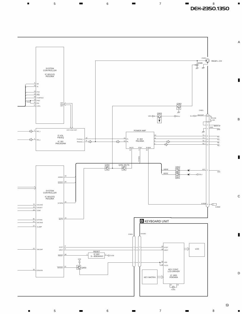
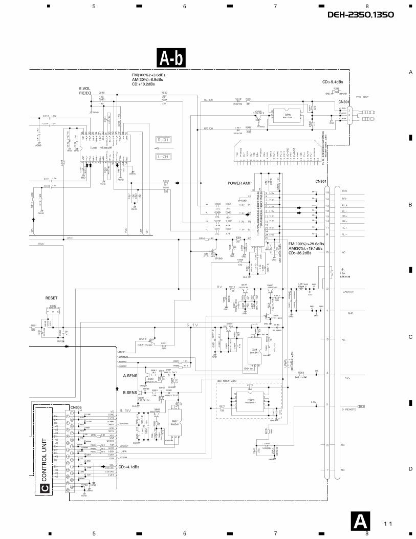
3. BLOCK DIAGRAM AND SCHEMATIC DIAGRAM
3.1 BLOCK DIAGRAM
M
M
M
LDMD
HOLOGRAMUNIT
FOCUS ACTTRACKING ACT
LD+
MD
FO+
TO+
14
5
4
3
SPINDLEMOTOR
CARRIAGEMOTOR
LOADINGMOTOR
1
2
3
4
3
1
2
SELECTSENSE
DISC SENSE
D
CN801
CN802
D802 D801
VD
S802CLAMP
6
5
11
22
23
21
1
28
21
CDLOAD
CDEJET
CONT
EJTSNS
DSCSNS
CLAMP
CD5VON
VDCONT
VDD IC 701BA05SFP
IN
+5V REGULATOR
24
1
VD
Q981
Q982
B.U
ANTENNA CN402
A
LOCL
Q411
VCC VDD
PC
E2
PC
K
PC
E1
SL
SD
PD
IO
C
Q101CN101
FOP
TOP
A+C/F
B+D/E
98LD L_OUT
PD
HOME
97
24
23
39
X201
TD/FD
SD/MD
RF-AMP, DSP,SERVO, DAC
IC 201UPD63711GC
16CN701 CN605
17
1
8
24
CDL
IC 301BA5985FM
S801HOME12
16
18
11
14
13
10
9
SOP
TOP
FOP
SOM
COP
COM
LOP
LOM
FWD
REV
MUTE
CD
DR
IVE
R
7 18
19
20
14
3
2
4
CLAMP
DINC
EJTD
CDLOAD
EJET
CONT
PDIO
TUNER AMP UNIT
CONTROL UNITPICKUP UNIT(SERVICE)(P8)
PHOTO UNIT(S8)
4
VD
CD5VON
IC 3EEPROM
FM/AM TUNER UNIT
28
27
FM/AM 1ST IF 10.7MHzT51 Q51 CF51 CF52 CF53
IC1MIXER, IF AMP, DET.
6
21
18LDET
COMP
2225 10 14 12 15 16 8 13 2 3 4
CF202
VDDVCC
DI/D
O
CE
2
CK
CE
1
SD
BW
SL
FMS
D
NL1
NL2
IC 2 FM MPX
AMANT
FMANT
ATT
ATT
AMRF
FMRF
IMG ADJ
RF ADJ
X90110.25MHz
ANT ADJ
LOCL23
LOCH
AMDETMPXREF 41kHz
AM 2ND IF450kHz
19
CR
EQ
11
DG
ND
1
ST
IND
L ch
5R ch
924
NC
FMLO
CL
20177
NC
NC
WC
26 RFGND
9
DEH-2350,13505 6 7 8
5 6 7 8
D
C
B
A
KYDT
DPDT
KEY CONT. LCD DRIVER
IC 1801PD6340A
3
4
5
3
4
5
KEY MATRIX
SD
SL
PCE
PCK
TUNPCE2
PDO
LOCL
IN2_L
IN3_L
6
76
14
13
48
12
57
2
3
SYSTEMCONTROLLER
IC 601(1/2)PE5196A
VSTVCKVDT
B.UVDD
Q903B.U
BACKUP
FL—
FL+
RL—
RL+
ACC
2
1
9
11
10
12
4
E.VOLFIE/EQ
IC 301PML003AM
SYSTEMCONTROLLER
IC 601(2/2)PE5196A
ASENS63
BSENS64
SYSPW42
MUTE44
KYDT8
DPDT9
RESET60
SWVDD41
Frontout_L10
Rearout_L11
POWER AMP
IC 302PAL006A
14
12
22 4
5
3
21
23
FL
MUTE STBY
25
B.REM
RL
B.Ubsens
asens
Q902Q351 MUTEQ350
B KEYBOARD UNIT
CN1801CN601
LCD
22 23
X1801
20
18
Q650
RESETIC 602
S—80834ANY VDD1 2
SY
SP
W
GND
5B.REM
FUSE10A
CD5VON
31
34
23
80
79
27
22
35
VDCONT
CLAMP
DSCSNS
EJTSNS
CDLOAD
CDEJET
CONT
PDI11PDIO
VST/ VCK/ VDT
Q901
VDD
VDD
VLCD
56
10
CN901
Q346
CN301
REAR L CH
Q363
BACK UP
FL–
FL+
RL–
RL+
B.REM
ACC
GND

10
DEH-2350,13501 2 3 4
1 2 3 4
D
C
B
A
3.2 OVERALL CONNECTION DIAGRAM(GUIDE PAGE)Note: When ordering service parts, be sure to refer to “EXPLODED VIEWS AND PARTS LIST” or “ELECTRICAL PARTS
LIST”.
A-a A-b
A-aA-a A-b A-b
A-b A-b A-a A-a
Large sizeSCH diagram
Guide page
Detailed page
A
DS
P-2
01M
-S00
B
183
162
162
183
272
272
273
203
PE5196A
CN601
CN403
CN402
FM(100%):-19.5dBsAM(30%):-30dBs
SYSTEM CONTROLLER
For resistors and capacitors in the circuit diagrams, their resistance values orcapacitance values are expressed in codes:
Ex. *Resistors Code Practical value 123 12k ohms 103 10k ohms
*Capacitors Code Practical value 103 0.01µF 101/10 100µF/10V
The > mark found on some component parts indicatesthe importance of the safety factor of the part.Therefore, when replacing, be sure to use parts ofidentical designation.
Symbol indicates a resistor.No differentiation is made between chip resistors anddiscrete resistors.
NOTE :
Symbol indicates a capacitor.No differentiation is made between chip capacitors anddiscrete capacitors.
KEYBOARDUNIT
B
FM/AM TUNER UNIT
A-aTUNER AMP UNITA
11
DEH-2350,13505 6 7 8
5 6 7 8
D
C
B
A
A
332/
16
B.R
EM
(DE
H-2
350/
X1M
/ES
)N
C(D
EH
-135
0/X
1M/E
S)
Pin
25
:
PA
L006
A(D
EH
-235
0/X
1M/E
S)
TD
A73
86(D
EH
-135
0/X
1M/E
S)
600µH
331/
16
CN901
CN301
CN605
CEK1136
>
(DE
H-2
350/
X1M
/ES
)
(DE
H-2
350/
X1M
/ES
)
(DEH-1350/X1M/ES)
FM(100%):+3.6dBsAM(30%):-6.9dBsCD:+10.2dBs
FM(100%):+29.6dBsAM(30%):+19.1dBsCD:+36.2dBs
CD:+4.1dBs
CD:+9.4dBs
RESET
E.VOLFIE/EQ
POWER AMP
A.SENS
B.SENS
CO
NT
RO
L U
NIT
C
A-b

12
DEH-2350,13501 2 3 4
1 2 3 4
D
C
B
A
A-a
A-a
A-b
1
DSP-201M-S00B
183
162162
183
272
272
CN
403
CN
402
FM(1
00%
):-1
9.5d
Bs
AM
(30%
):-3
0dB
s
FM/A
M T
UN
ER
UN
IT
TU
NE
R A
MP
UN
ITA

13
DEH-2350,13505 6 7 8
5 6 7 8
D
C
B
A
A-a
A-a
A-b
273203
PE
5196
A
CN
601
SY
ST
EM
CO
NT
RO
LLE
R
RE
SE
For
resi
sto
rs a
nd
cap
acit
ors
in t
he
circ
uit
dia
gra
ms,
th
eir
resi
stan
ce v
alu
es o
rca
pac
itan
ce v
alu
es a
re e
xpre
ssed
in c
od
es:
Ex.
*R
esis
tors
C
od
e
P
ract
ical
val
ue
1
23
12k
oh
ms
1
03
10k
oh
ms
*C
apac
ito
rs
Co
de
P
ract
ical
val
ue
1
03
0.01
µF
101
/10
10
0µF/
10V
Th
e >
mar
k fo
un
d o
n s
om
e co
mp
on
ent
par
ts in
dic
ates
the
imp
ort
ance
of
the
safe
ty f
acto
r o
f th
e p
art.
Th
eref
ore
, wh
en r
epla
cin
g, b
e su
re t
o u
se p
arts
of
iden
tica
l des
ign
atio
n.
Sym
bo
l in
dic
ates
a r
esis
tor.
No
dif
fere
nti
atio
n is
mad
e b
etw
een
ch
ip r
esis
tors
an
dd
iscr
ete
resi
sto
rs.
NO
TE
: Sym
bo
l in
dic
ates
a c
apac
ito
r.N
o d
iffe
ren
tiat
ion
is m
ade
bet
wee
n c
hip
cap
acit
ors
an
dd
iscr
ete
cap
acit
ors
.
KE
YB
OA
RD
UN
IT
B
CONTROL UNIT C
2

14
DEH-2350,13501 2 3 4
1 2 3 4
D
C
B
A
A-a
A-b
A-b
332/16
B.REM(DEH-2350/X1M/ES)NC(DEH-1350/X1M/ES)
Pin 25 :
PAL006A(DEH-2350/X1M/ES)TDA7386(DEH-1350/X1M/ES)
600µ
H
CN
901
CN
301
CE
K11
36
>
(DEH-2350/X1M/ES)
FM(1
00%
):+3
.6d
Bs
AM
(30%
):-6
.9d
Bs
CD
:+10
.2d
Bs
FM(1
00%
):+2
9.6d
Bs
AM
(30%
):+1
9.1d
Bs
CD
:+36
.2d
Bs
CD
:+9.
4dB
s
E.V
OL
FIE
/EQ
PO
WE
R A
MP
1

15
DEH-2350,13505 6 7 8
5 6 7 8
D
C
B
A
A-b
A-a
A-b
600µ
H
331/16
CN
605
CE
K11
36
(DEH-2350/X1M/ES)
(DE
H-1
350/
X1M
/ES
)
CD
:+4.
1dB
s
RE
SE
T
A.S
EN
S
B.S
EN
S
CONTROL UNIT C
2

16
DEH-2350,13501 2 3 4
1 2 3 4
D
C
B
A
3.3 KEYBOARD UNIT
KEYBOARD UNIT
LCD CAW1606(DEH-2350/X1M/ES), CAW1633(DEH-1350/X1
LCD DRIVERKEY CONTROLLER
B
B

17
DEH-2350,13505 6 7 8
5 6 7 8
D
C
B
A
AC
N60
1
50/X1M/ES)
IL1801, 1802:CEL1651(14V 40mA)
R17
08, 1
710,
171
2:15
1
D17
01-1
708:
SM
L210
PT
CLK
BSM
EQ
LOUD
B
DEH-2350,13501 2 3 4
1 2 3 4
D
C
B
A
BA05SFP
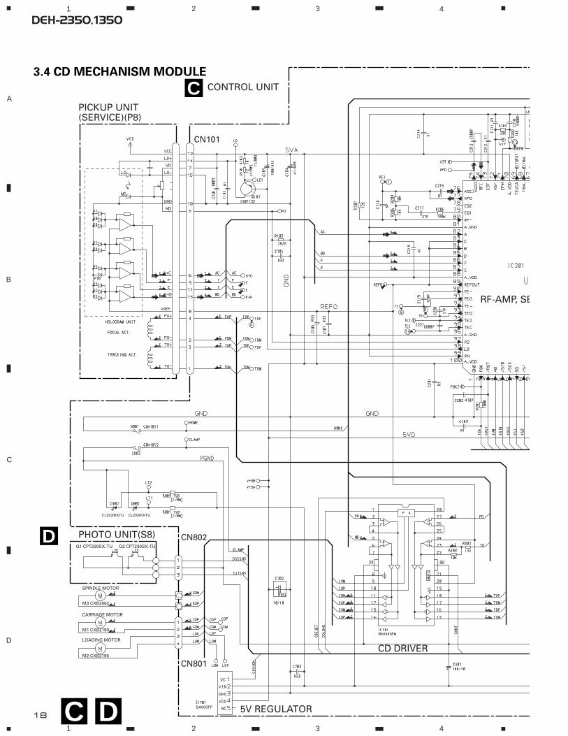
(SERVICE)(P8)PICKUP UNIT
PHOTO UNIT(S8)
CONTROL UNIT
SPINDLE MOTOR
Q2 CPT230SX-TUQ1 CPT230SX-TU
M3 CXB2562
CARRIAGE MOTOR
M1 CXB2190
M2 CXB2195
LOADING MOTOR
RF-AMP, SE
5V REGULATOR
CD DRIVER
CN101
CN802
CN801
CL203IRXTU CL203IRXTU
3.4 CD MECHANISM MODULE
D
D
C
18 C
DEH-2350,13505 6 7 8
5 6 7 8
D
C
B
A
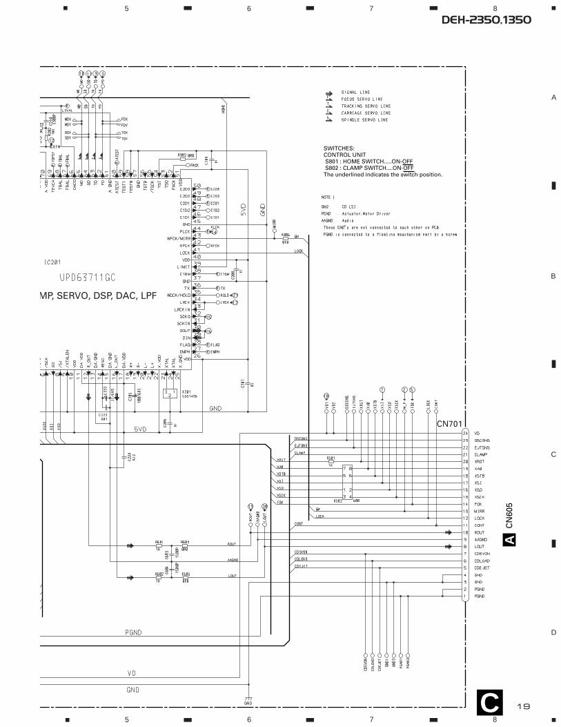
MP, SERVO, DSP, DAC, LPF
SWITCHES:CONTROL UNIT S801 : HOME SWITCH.....ON-OFF S802 : CLAMP SWITCH....ON-OFFThe underlined indicates the switch position.
CN701
CN
605
A
19C

20
DEH-2350,1350
1 RFI 0.5V/div. 0.5µs/div.Normal mode: play
1 CH1: RFI 1V/div.2 CH2: MIRR 5V/div.
Test mode: Tracking open
0.5ms/div. 1 CH1: RFI 1V/div.2 CH2: MIRR 5V/div.
Normal mode: The defect partpasses 800µm
0.5ms/div.
3 CH1: FD 0.5V/div.4 CH2: FO+ 2V/div.
Test mode: No disc, Focus close
0.2s/div. 3 CH1: FD 0.5V/div.5 CH2: FOK 2V/div.
Normal mode: Focus close
0.2s/div. 6 CH1: FE 0.5V/div.7 CH2: XSI 2V/div.
Normal mode: Focus close
1ms/div.
REFO →
8 CH1: TE 0.5V/div.9 CH2: TD 0.5V/div.
Test mode: 32 tracks jump (FWD)
0.5ms/div. 8 CH1: TE 0.5V/div.9 CH2: TD 0.5V/div.
Test mode: Single jump (FWD)
0.5ms/div. 8 CH1: TE 0.5V/div.9 CH2: TD 0.5V/div.
Test mode: 100 tracks jump (FWD)
5ms/div.
6 CH1: FE 0.1V/div.3 CH2: FD 0.2V/div.
Normal mode: Play
20ms/div. 3 CH1: FD 0.5V/div.0 CH2: MD 1V/div.
Normal mode: Focus close (12cm)
0.5s/div. 3 CH1: FD 0.5V/div.0 CH2: MD 1V/div.
Normal mode: Focus close (8cm)
0.5s/div.
REFO →
REFO →
REFO →
REFO →
REFO →
REFO →
GND →
REFO →
REFO →
REFO →
REFO →
REFO →
REFO →
REFO →
REFO →
REFO →
REFO →
REFO →
REFO →
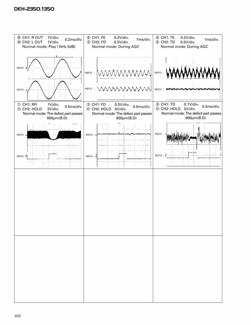
- Waveforms
Note:1. The encircled numbers denote measuring pointes in the circuit diagram.2. Reference voltage
REFO:2.5V
REFO →
REFO →
REFO →
REFO →

21
DEH-2350,1350
8 CH1: TE 0.2V/div.9 CH2: TD 0.2V/div.
Normal mode: play
8 CH1: TE 0.5V/div.! CH2: SD 0.5V/div.TEST mode: 100 Tracks jump(FWD)
5ms/div. 0 MD 0.5V/div. 0.1s/div.
Normal mode: Play (12cm)
0 MD 1V/div. 10ms/div.Normal mode:Long Search (12cm)
@ EFM 1V/div. 5µs/div.
Normal mode: play
8 CH1: TE 1V/div.# CH2: TEC 1V/div.
Test mode: Focus closeTracking open
2ms/div.
8 CH1: TE 0.5V/div.6 CH2: FE 0.5V/div.
Normal mode: AGC after focus close
0.2s/div.$ PLCK 2V/div. 0.5µs/div.
Normal mode: play
20ms/div.
% SCKO 2V/div. 1µs/div.
Normal mode: play
^ Dout 2V/div. 10µs/div.
Normal mode: play
& LRCK 2V/div. 20µs/div.
Normal mode: play
* VD 5V/div. 50ms/div.
Normal mode: No disc
GND →
REFO →
REFO →
GND →
REFO →
REFO →
REFO →
REFO →REFO →
REFO →
REFO →
REFO →
REFO →
GND →
REFO →
GND →
REFO →
GND →
REFO →
GND →
REFO →
22
DEH-2350,1350
( CH1: R OUT 1V/div.) CH2: L OUT 1V/div.
Normal mode: Play (1kHz 0dB)
6 CH1: FE 0.2V/div.3 CH2: FD 0.5V/div.
Normal mode: During AGC
1ms/div. 8 CH1: TE 0.2V/div.9 CH2: TD 0.5V/div.
Normal mode: During AGC
1 CH1: RFI 1V/div.⁄ CH2: HOLD 5V/div.
Normal mode: The defect part passes800µm(B.D)
0.2ms/div. 1ms/div.
0.5ms/div. 3 CH1: FD 0.5V/div.⁄ CH2: HOLD 5V/div.
Normal mode: The defect part passes800µm(B.D)
0.5ms/div.9 CH1: TD 0.1V/div.⁄ CH2: HOLD 5V/div.
Normal mode: The defect part passes800µm(B.D)
0.5ms/div.
REFO →
REFO →
REFO →
REFO →
REFO →
REFO →
REFO →
REFO → REFO →
REFO →
REFO →
REFO →

23
DEH-2350,1350

24
DEH-2350,13501 2 3 4
1 2 3 4
D
C
B
A
NOTE FOR PCB DIAGRAMS
1. The parts mounted on this PCB
include all necessary parts for
several destination.
For further information for
respective destinations, be
sure to check with the
schematic diagram.
2. Viewpoint of PCB diagrams
A
CapacitorConnector
P.C.Board Chip Part
SIDE A
SIDE B
1 3 5 7 9 11 13 15
2
4 6 8 10 12 14 16
CN1801BCN701C
CORD ASSY
4. PCB CONNECTION DIAGRAM
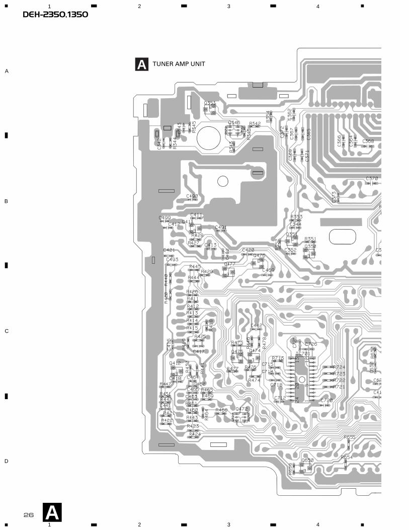
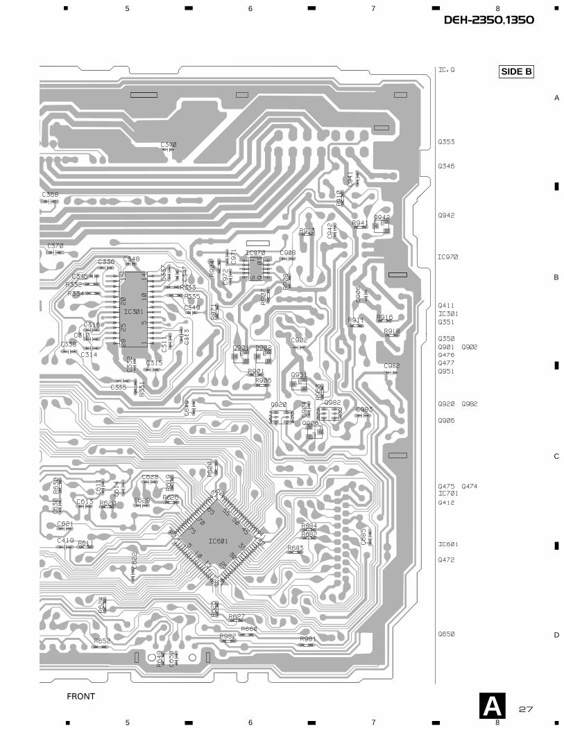
4.1 TUNER AMP UNIT
A TUNER AMP UNIT
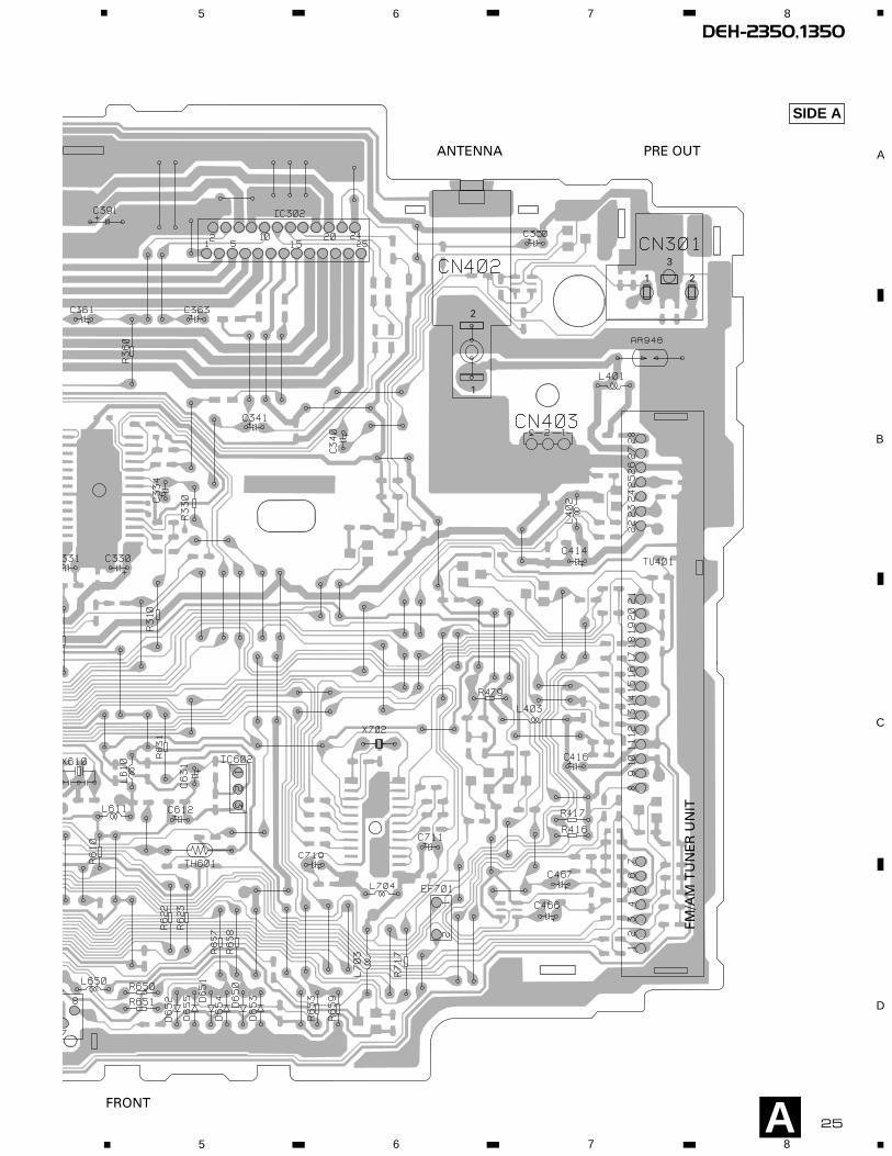
25
DEH-2350,13505 6 7 8
5 6 7 8
D
C
B
A
AFRONT
1
2
3
1 2
FM/A
M T
UN
ER
UN
IT
SIDE A
ANTENNA PRE OUT
26
DEH-2350,13501 2 3 4
1 2 3 4
D
C
B
A
A
456
321
123
654
A TUNER AMP UNIT
27
DEH-2350,13505 6 7 8
5 6 7 8
D
C
B
A
A
123
654
456
321
FRONT
SIDE B

28
DEH-2350,13501 2 3 4
1 2 3 4
D
C
B
A
LOU
DVO
L-
VO
L-S
OU
RC
E SO
UR
CE
12
34
56
CLK
BS
ME
JEC
T
BANDAUDIO
←→
↑ ↓
VO
L+
VO
L+E
Q
4.2 KEYBOARD UNIT SIDE A
KE
YB
OA
RD
UN
IT
B
B

29
DEH-2350,13501 2 3 4
1 2 3 4
D
C
B
A
B
B
CN
601
A
SIDE B
KE
YB
OA
RD
UN
IT
30
DEH-2350,13501 2 3 4
1 2 3 4
D
C
B
A
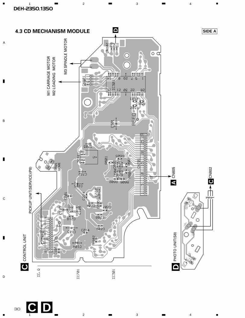
4.3 CD MECHANISM MODULE
CO
NT
RO
L U
NIT
HO
ME
M1
CA
RR
IAG
E M
OT
OR
M2
LOA
DIN
G M
OT
OR
M3
SP
IND
LE M
OT
OR
PIC
KU
P U
NIT
(SE
RV
ICE
)(P
8)
CN
802
CN
605
3 2 1
PH
OT
O U
NIT
(S8)
SIDE A
D
D
C
C
C
D
A

31
DEH-2350,13501 2 3 4
1 2 3 4
D
C
B
A
CLA
MP
SIDE B
CO
NT
RO
L U
NIT
C
C

32
DEH-2350,1350
5. ELECTRICAL PARTS LIST
NOTES:
- Parts whose parts numbers are omitted are subject to being not supplied.
- The part numbers shown below indicate chip components.
Chip Resistor
RS1/_S___J,RS1/__S___J
Chip Capacitor (except for CQS.....)
CKS....., CCS....., CSZS.....
=====Circuit Symbol and No.===Part Name Part No.--- ------ ------------------------------------------ -------------------------
Unit Number : CWM7293(DEH-2350/X1M/ES): CWM7297(DEH-1350/X1M/ES)
Unit Name : Tuner Amp Unit
MISCELLANEOUS
IC 301 IC PML003AMIC 302 IC(DEH-2350/X1M/ES) PAL006AIC 302 IC(DEH-1350/X1M/ES) TDA7386IC 601 IC PE5196AIC 602 IC S-80834ANY
IC 970 IC(DEH-1350/X1M/ES) TPD1018FQ 346 Transistor RN1610Q 350 Transistor DTA124EKQ 351 Transistor DTC114EKQ 353 Transistor DTA124EK
Q 411 Transistor 2SC2412KQ 650 Transistor 2SA1037KQ 901 Transistor 2SC2412KQ 902 Transistor 2SC2412KQ 903 Transistor 2SD1859
Q 904 Transistor 2SD2396Q 905 Transistor 2SB1243Q 906 Transistor DTC114EKQ 920 Transistor RN46A1Q 981 Transistor 2SD2396
Q 982 Transistor RN46A1D 650 Diode 1SS270D 651 Diode 1SS270D 652 Diode 1SS270D 653 Diode 1SS270
D 654 Diode 1SS270D 655 Diode 1SS270D 901 Diode HZS7L(C2)D 902 Diode S5688GD 903 Diode S5688G
D 904 Diode HZS7L(A1)D 905 Diode S5688GD 906 Diode HZS6L(B2)D 907 Diode HZS9L(B3)D 941 Diode S5688G
D 942 Diode S5688GD 981 Diode HZS9L(B1)L 310 Ferri-Inductor LAU1R0ML 401 Ferri-Inductor LAU4R7KL 402 Ferri-Inductor LAU2R2K
L 403 Inductor LAU100KL 610 Ferri-Inductor LAU101KL 611 Ferri-Inductor LAU2R2KL 650 Ferri-Inductor LAU2R2KL 901 Choke Coil 600µH CTH1221
X 610 Crystal Resonator 4.194304MHz CSS1023AR 946 Arrester DSP-201M-S00B
FM/AM Tuner Unit CWE1563
RESISTORS
R 310 RD1/4PU222JR 311 RD1/4PU222JR 332 RS1/16S221JR 333 RS1/16S221JR 334 RS1/16S221J
R 335 RS1/16S221JR 342 RS1/16S681JR 343 RS1/16S681JR 344 RS1/16S223JR 345 RS1/16S223J
R 346 RS1/16S0R0JR 351 RS1/16S102JR 352 RS1/16S103JR 353 RS1/16S103JR 354 RS1/16S331J
R 360 RD1/4PU153JR 411 RS1/16S681JR 412 RS1/16S681JR 413 RS1/16S681JR 414 RS1/16S103J
R 415 RS1/16S681JR 416 RD1/4PU473JR 417 RD1/4PU472JR 418 RS1/16S473JR 419 RS1/16S473J
R 420 RS1/16S473JR 421 RS1/16S473JR 422 RS1/16S473JR 423 RS1/16S681JR 424 RS1/16S681J
R 425 RS1/16S393JR 427 RS1/16S222JR 428 RS1/16S222JR 460 RS1/16S272JR 461 RS1/16S272J
R 464 RS1/16S162JR 465 RS1/16S162JR 468 RS1/16S0R0JR 469 RS1/16S0R0JR 610 RD1/4PU203J
R 611 RS1/16S273JR 619 RS1/16S0R0JR 620 RS1/16S223JR 622 RD1/4PU222JR 623 RD1/4PU222J
R 624 RS1/16S473JR 625 RS1/16S473JR 626 RS1/16S473JR 627 RS1/16S473JR 628 RD1/4PU222J
=====Circuit Symbol and No.===Part Name Part No.--- ------ ------------------------------------------ -------------------------
A
33
DEH-2350,1350
R 629 RS1/16S473JR 630 RS1/16S822JR 631 RD1/4PU102JR 649 RS1/16S222JR 650 RD1/4PU222J
R 651 RD1/4PU222JR 652 RS1/16S472JR 653 RD1/4PU222JR 654 RS1/16S473JR 655 RS1/16S103J
R 656 RS1/16S103JR 657 RD1/4PU102JR 658 RD1/4PU102JR 660 RS1/16S1R0JR 681 RD1/4PU681J
R 682 RS1/16S102JR 683 RS1/16S102JR 684 RS1/16S102JR 901 RS1/16S104JR 902 RD1/4PU104J
R 903 RD1/4PU103JR 904 RS1/16S473JR 905 RD1/4PU102JR 906 RS1/16S473JR 907 RS1/16S473J
R 908 RS1/16S472JR 909 RD1/4PU103JR 910 RS1/16S0R0JR 911 RS1/16S122JR 912 RD1/4PU103J
R 913 RS1/16S101JR 914 RD1/4PU152JR 916 RS1/16S221JR 918 RS1/16S1R0JR 944 RD1/4PU152J
R 971 (DEH-1350/X1M/ES) RS1/16S103JR 981 RS1/16S472JR 982 RS1/16S222JR 983 RD1/4PU221JR 984 RD1/4PU221J
CAPACITORS
C 310 CKSRYB105K6R3C 311 CKSRYB104K16C 313 CKSRYB105K6R3C 314 CKSRYB104K16C 315 CKSRYB102K50
C 316 CKSRYB102K50C 330 CEJA470M10C 331 CEJA100M16C 332 CKSRYB104K16C 333 CEJA4R7M35
C 334 CEJA4R7M35C 336 CKSRYB153K25C 337 CKSRYB153K25C 340 CEAL2R2M50C 341 CEJA2R2M50
C 346 CCSRCH100D50C 347 CCSRCH100D50C 348 CCSRCH100D50C 349 CCSRCH100D50C 350 CEJA330M10
C 361 CEJA2R2M50C 362 CKSQYB225K10C 363 CEJA100M16C 364 CKSQYB474K16C 365 CKSQYB474K16
C 366 CKSQYB474K16C 367 CKSQYB474K16C 368 CKSQYB474K16C 369 CKSQYB474K16C 370 CKSQYB474K16
C 371 CKSQYB474K16C 372 CKSQYB225K10C 373 (DEH-2350/X1M/ES) CKSRYB473K25C 390 CKSRYB104K16C 391 3300µF/16V CCH1368
C 411 CKSRYB223K25C 412 CKSRYB223K25C 413 CKSRYB102K50C 414 CEJA220M10C 415 CKSRYB473K16
C 416 CEAL101M10C 417 CKSRYB472K50C 419 CCSRCH101J50C 420 CCSRCH101J50C 462 CKSRYB183K25
C 463 CKSRYB183K25C 490 CKSQYB103K50C 499 CKSRYB103K50C 612 CEJA4R7M35C 613 CKSRYB473K16
C 614 CCSRCH101J50C 628 CCSRCH150J50C 629 CCSRCH150J50C 630 CKSRYB473K16C 631 CEAL2R2M50
C 650 CKSRYB104K16C 901 CEJA101M10C 902 CKSRYB473K16C 903 470µF/16V CCH1331C 904 CKSRYB473K16
C 905 330µF/16V CCH1326C 906 CKSRYB103K50C 907 CEJA101M16C 941 CKSRYB473K16C 971 (DEH-1350/X1M/ES) CKSRYB103K50
C 972 (DEH-1350/X1M/ES) CKSRYB473K16C 981 CEJA101M10C 982 CKSRYB102K50C 983 CKSRYB473K16
Unit Number : CWM7303(DEH-2350/X1M/ES): CWM7307(DEH-1350/X1M/ES)
Unit Name : Keyboard Unit
MISCELLANEOUS
IC 1801 IC PD6340AD 1701 LED SML210PTD 1702 LED SML210PTD 1703 LED SML210PTD 1704 LED SML210PT
D 1705 LED SML210PTD 1706 LED SML210PTD 1707 LED SML210PTD 1708 LED SML210PTD 1801 Diode MA152WK
D 1802 Diode MA152WAD 1811 LED NSSW440-9159D 1812 LED NSSW440-9159X 1801 Ceramic Resonator 4.97MHz CSS1422IL 1801 Lamp 14V 40mA CEL1651
IL 1802 Lamp 14V 40mA CEL1651LCD(DEH-2350/X1M/ES) CAW1606LCD(DEH-1350/X1M/ES) CAW1633
=====Circuit Symbol and No.===Part Name Part No.--- ------ ------------------------------------------ -------------------------
=====Circuit Symbol and No.===Part Name Part No.--- ------ ------------------------------------------ -------------------------
B

34
DEH-2350,1350
RESISTORS
R 1701 RS1/16S151JR 1702 RS1/16S181JR 1703 RS1/16S181JR 1704 RS1/16S181JR 1705 RS1/16S181J
R 1706 RS1/16S151JR 1707 RS1/16S151JR 1708 RS1/16S151JR 1709 RS1/16S181JR 1710 RS1/16S151J
R 1711 RS1/16S181JR 1712 RS1/16S151JR 1713 RS1/16S131JR 1801 RS1/16S222JR 1802 RS1/16S222J
R 1803 RS1/16S471JR 1804 RS1/16S471JR 1805 RS1/16S471JR 1806 RS1/16S471J
CAPACITORS
C 1801 CKSRYB103K50C 1811 CKSQYF104Z25C 1812 CKSQYF104Z25
Unit Number : CWX2411Unit Name : Control Unit
MISCELLANEOUS
IC 201 IC UPD63711GCIC 301 IC BA5985FMIC 701 IC BA05SFPQ 101 Transistor 2SB1132D 801 LED CL203IRXTU
D 802 LED CL203IRXTUX 201 Ceramic Oscillator 16.934MHz CSS1456S 801 Spring Switch(HOME) CSN1051S 802 Spring Switch(CLAMP) CSN1052
RESISTORS
R 101 RS1/8S120JR 102 RS1/8S100JR 103 RS1/16S222JR 201 RS1/16S104JR 202 RS1/16S103J
R 203 RS1/16S393JR 204 RS1/16S103JR 205 RS1/16S103JR 206 RS1/16S182JR 207 RS1/16S123J
R 302 RS1/16S153JR 303 RS1/16S103JR 501 RS1/16S102JR 502 RA4C681JR 601 RS1/16S102J
R 602 RS1/16S102JR 605 RS1/16S0R0JR 606 RS1/16S0R0JR 801 RS1/8S751JR 803 RS1/8S751J
R 902 RS1/16S0R0JR 906 RS1/16S0R0J
CAPACITORS
C 101 CKSRYB102K50C 102 CKSRYB104K16C 103 CEV101M6R3C 104 CEV470M6R3C 105 CKSQYB334K16
C 106 CKSQYB334K16C 107 CKSQYB334K16C 201 CKSRYB104K16C 202 CKSRYB471K50C 203 CKSRYB104K16
C 205 CEV101M6R3C 206 CKSRYB104K16C 207 CKSRYB104K16C 208 CKSRYB104K16C 209 CKSRYB104K16
C 210 CKSRYB332K50C 211 CKSRYB104K16C 212 CKSRYB104K16C 213 CKSRYB392K50C 214 CKSRYB104K16
C 215 CKSRYB104K16C 216 CCSRCJ3R0C50C 217 CCSRCH270J50C 218 CKSRYB104K16C 219 CCSRCH181J50
C 220 CCSRCH510J50C 221 CKSRYB682K25C 222 CEV220M6R3C 223 CKSRYB103K25C 224 CKSRYB224K10
C 301 CEV101M10C 603 CCSQSL152J50C 604 CCSQSL152J50C 702 10µF/10V CCH1349C 703 CKSQYB334K16
Unit Number :Unit Name : Photo Unit(S8)
Q 1 Photo-transistor CPT230SX-TUQ 2 Photo-transistor CPT230SX-TU
Miscellaneous Parts List
Pickup Unit(Service)(P8) CXX1285M 1 Motor Unit(CARRIAGE) CXB2190M 2 Motor Unit(LOADING) CXB2195M 3 Motor Unit(SPINDLE) CXB2562
Fuse(10A) CEK1136
=====Circuit Symbol and No.===Part Name Part No.--- ------ ------------------------------------------ -------------------------
=====Circuit Symbol and No.===Part Name Part No.--- ------ ------------------------------------------ -------------------------
C
D

35
DEH-2350,1350
1) Precautions• This unit uses a single power supply (+5V) for the reg-
ulator. The signal reference potential, therefore, isconnected to REFO(approx. 2.5V) instead of GND.If REFO and GND are connected to each other by mis-take during adjustments, not only will it be impossi-ble to measure the potential correctly, but the servowill malfunction and a severe shock will be applied tothe pick-up. To avoid this, take special note of the fol-lowing.Do not connect the negative probe of the measuringequipment to REFO and GND together. It is especiallyimportant not to connect the channel 1 negativeprobe of the oscilloscope to REFO with the channel 2negative probe connected to GND.Since the frame of the measuring instrument is usual-ly at the same potential as the negative probe, changethe frame of the measuring instrument to floating sta-tus.If by accident REFO comes in contact with GND,immediately switch the regulator or power OFF.
• Always make sure the regulator is OFF when connect-ing and disconnecting the various filters and wiringrequired for measurements.
• Before proceeding to further adjustments and mea-surements after switching regulator ON, let the playerrun for about one minute to allow the circuits to stabi-lize.
• Since the protective systems in the unit's software arerendered inoperative in test mode, be very careful toavoid mechanical and /or electrical shocks to the sys-tem when making adjustment.
• Disc detection during loading and eject operations isperformed by means of a photo transistor in thisunit.Consequently, if the inside of the unit is exposedto a strong light source when the outer casing isremoved for repairs or adjustment, the following mal-functions may occur.
*During PLAY, even if the eject button ispressed,the disc will not be ejected and the unitwill remain in the PLAY mode.
*The unit will not load a disc.When the unit malfunctions this way, either re-posi-tion the light source, move the unit or cover the phototransistor.
2) Test ModeThis mode is used for adjusting the CD mechanismmodule of the device.
• Test mode starting procedureReset while pressing the 4 and 6 keys together.
• Test mode cancellationSwitch ACC, back-up OFF.
• After pressing the EJECT key, do not press any otherkey until the disk is completely ejected.
• If the ] or [ key is pressed while focus search is inprogress, immediately turn the power off (otherwisethe actuator may be damaged due to adhesion of thelenses).
• Jump operation of TRs other than 100TR continuesafter releasing the key. CRG move and 100TR jumpoperations are brought into the “Tracking close” sta-tus when the key is released.
• Powering Off/On resets the jump mode to “1TR”, andthe automatic adjustment value to the initial value.
6. ADJUSTMENT
6.1 CD ADJUSTMENT

36
DEH-2350,1350
- Flow Chart
4
3
Reset
SOURCE
New test mode
6
[
BAND
BAND
BAND
BAND
BAND
3
*2*1
6
6
6
6
1
2
1
2]
] [
Select CD
Focus ModeSelect
Focus Close/S Curve Check
CRG- Auto AdjustmentDisplay Select
<Tracking Servo Close> CRG+
RF AGC Coefficient Display/Rough Servo and RF AGC
Tracking Open
TrackingOpen
T. Close andFit Servo
] [
1
3
Display
2
3
Displayor
8x 8x 8xTRK SECMIN
9x 9x 9xTRK SECMIN
or
CRG-CRG+ T.BalanceAdjustment
*4F, T, RF AGC/F.Bias Display Select
F, T AGC andRF AGC
Power ON(Adjustment for T.Offset)
*5 *6 *6
*7CRG/TR Jump NO.Select
CRG+/TR Jump+
CRG-/TR Jump-
Power OFF
Display
Display
Display
T.Close andF,T AGC andRF AGC andFit Servo
Power ON(Not adjustment for T.Offset)
Display
Display
2
Power OFF
Power OFF
Power OFF 8x 8x 8xTRK SECMIN
9x 9x 9xTRK SECMIN
8x 8x 8xTRK SECMIN
9x 9x 9xTRK SECMIN
or
8x 8x 8xTRK SECMIN
9x 9x 9xTRK SECMIN
or
00 00 00TRK SECMIN
99 99 99TRK SECMIN
or
00 00 00TRK SECMIN
99 99 99TRK SECMIN
or
00 00 00TRK SECMIN
99 99 99TRK SECMIN
or
91 91 91TRK SECMIN
0x 0x 0xTRK SECMIN
00 00 00TRK SECMIN
99 99 99TRK SECMIN
Test Mode In
*3
*1
*3
*6
*2
*5
*7
*4
F.Cancel T.Offset The original display
1TR/4TR/10TR/32TR/100TR"00", "99"→Focus Close / "01"→S.Curve
1TR 4TR91(81) 92(82)
CRG Move96(86)
100TR95(85)
32TR94(84)
10TR93(83)
Focus Close00(99)
LD Off02
S.Curve01
CRG Move,100TR Jump
TRK, MIN, SEC F.AGC Gain T.AGC Gain F.Bias
37
DEH-2350,1350
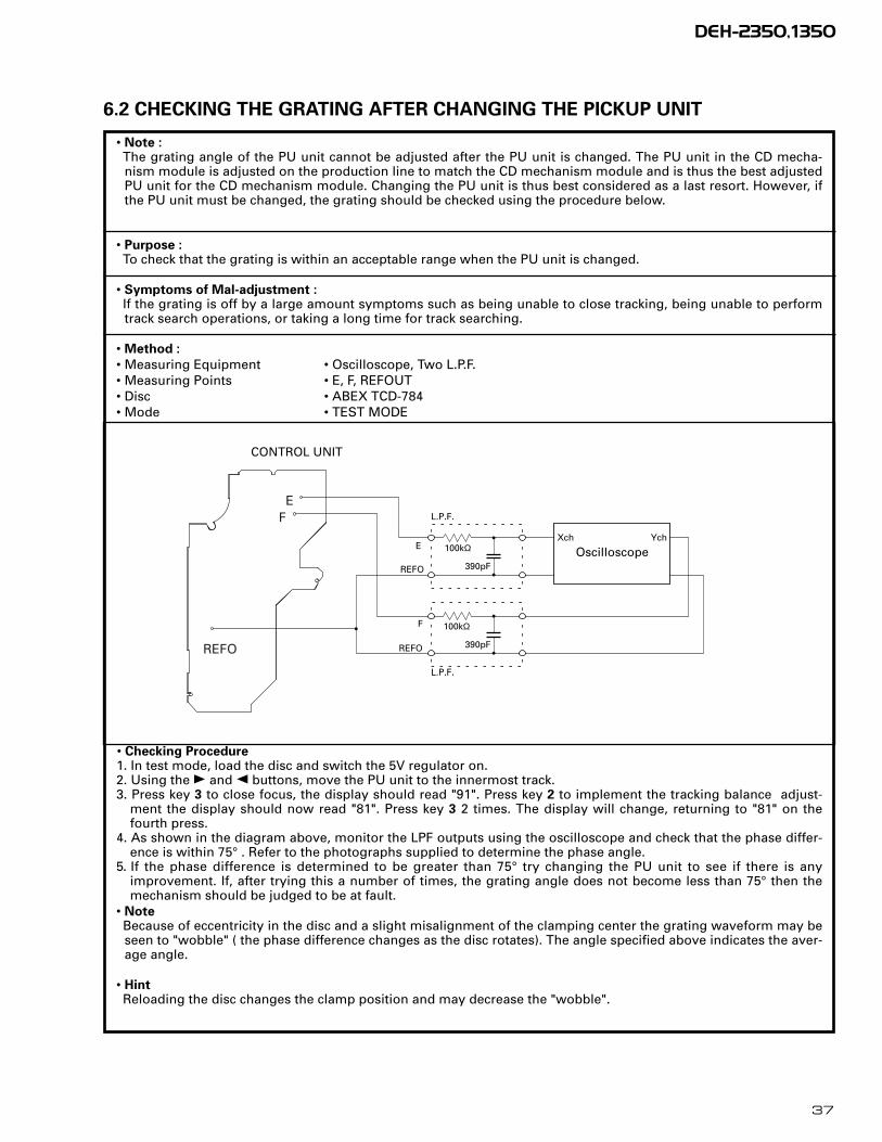
• Note :The grating angle of the PU unit cannot be adjusted after the PU unit is changed. The PU unit in the CD mecha-nism module is adjusted on the production line to match the CD mechanism module and is thus the best adjustedPU unit for the CD mechanism module. Changing the PU unit is thus best considered as a last resort. However, ifthe PU unit must be changed, the grating should be checked using the procedure below.
• Purpose :To check that the grating is within an acceptable range when the PU unit is changed.
• Symptoms of Mal-adjustment :If the grating is off by a large amount symptoms such as being unable to close tracking, being unable to performtrack search operations, or taking a long time for track searching.
• Method :
• Measuring Equipment • Oscilloscope, Two L.P.F.• Measuring Points • E, F, REFOUT• Disc • ABEX TCD-784• Mode • TEST MODE
• Checking Procedure1. In test mode, load the disc and switch the 5V regulator on.2. Using the ] and [ buttons, move the PU unit to the innermost track.3. Press key 3 to close focus, the display should read "91". Press key 2 to implement the tracking balance adjust-
ment the display should now read "81". Press key 3 2 times. The display will change, returning to "81" on thefourth press.
4. As shown in the diagram above, monitor the LPF outputs using the oscilloscope and check that the phase differ-ence is within 75° . Refer to the photographs supplied to determine the phase angle.
5. If the phase difference is determined to be greater than 75° try changing the PU unit to see if there is anyimprovement. If, after trying this a number of times, the grating angle does not become less than 75° then themechanism should be judged to be at fault.
• NoteBecause of eccentricity in the disc and a slight misalignment of the clamping center the grating waveform may beseen to "wobble" ( the phase difference changes as the disc rotates). The angle specified above indicates the aver-age angle.
• HintReloading the disc changes the clamp position and may decrease the "wobble".
F
REFO
E
100kΩ
390pF
100kΩ
390pF
E
REFO
F
REFO
L.P.F.
L.P.F.
CONTROL UNIT
Xch Ych
Oscilloscope
6.2 CHECKING THE GRATING AFTER CHANGING THE PICKUP UNIT

38
DEH-2350,1350
Grating waveform Ech → Xch 20mV/div, ACFch → Ych 20mV/div, AC
45°
0°
75°
60°
30°
90°

39
DEH-2350,1350
7. GENERAL INFORMATION
7.1 DIAGNOSIS
7.1.1 TEST MODE
- Error Messages
If a CD is not operative or stopped during operation due to an error, the error mode is turned on and cause(s) of the
error is indicated with a corresponding number. This arrangement is intended at reducing nonsense calls from the
users and also for facilitating trouble analysis and repair work in servicing.
(1) Basic Indication Method
1) When SERRORM is selected for the CSMOD (CD mode area for the system), error codes are written to DMIN (min-
utes display area) and DSEC (seconds display area). The same data is written to DMIN and DSEC. DTNO remains
in blank as before.
2) Head unit display examples
Depending on display capability of LCD used, display will vary as shown below. xx contains the error number.
8-digit display 6-digit display 4-digit display
ERROR–xx ERR–xx E–xx
OR
Err–xx
(2) Error Code List
Code Class Displayed error code Description of the code and potential cause(s)
10 Electricity Carriage Home NG CRG can't be moved to inner diameter.
CRG can't be moved from inner diameter.
→ Failure on home switch or CRG move mechanism.
11 Electricity Focus Servo NG Focusing not available.
→ Stains on rear side of disc or excessive vibrations on REWRITABLE.
12 Electricity Spindle Lock NG Spindle not locked. Sub-code is strange (not readable).
→ Failure on spindle, stains or damages on disc, or excessive vibrations.
Subcode NG A disc not containing CD-R data is found. Turned over disc are found,
though rarely.
→ Failure on home switch or CRG move mechanism.
RF AMP NG An appropriate RF AMP gain can't be determined.
→ CD signal error.
17 Electricity Setup NG APC protection doesn't work. Focus can be easily lost.
→ Damages or stains on disc, or excessive vibrations.
30 Electricity Search Time Out Failed to reach target address.
→ CRG tracking error or damages on disc.
A0 System Power Supply NG Power (VD) is ground faulted.
→ Failure on SW transistor or power supply (failure on connector).
Remarks: Mechanical errors are not displayed (because a CD is turned off in these errors).
Unreadable TOC does not constitute an error. An intended operation continues in this case.
A newly designed head unit must conform to the example given above.
Upper digits of an error code are subdivided as shown below:
1x: Setup relevant errors, 3x: Search relevant errors, 3x: Search relevant errors, Ax: Other errors.

40
DEH-2350,1350
- New Test Mode
S-CD plays the same way as before.
If an error such as off focus, spindle unlocking, unreadable sub-code, or sound skipping occurs after setup, its
cause and time occurred (in absolute time) are displayed.
During setup, operational status of the control software (internal RAM: CPOINT) is displayed.
These displays and functions are prepared for enhancing aging in the servicing and efficiency of trouble analysis.
(1) Shifting to the New Test Mode
1 Turn on the current test mode by starting the reset from the key.
2 Select S-CD for the source through the specified procedure including use of the [SOURCE] key, and inserting the
disc. Then, press the [Jump Mode Selector] key while maintaining the regulator turned off.
3 After the above operations, the new test mode remains on irrespective of whether the S-CD is turned on or off.
You can reset the new test mode by turning on the reset start.
* With some products, the new test mode can be reset through the same operations as that employed for shifting to
the STBY mode (while maintaining the Acc turned off).
(2) Key Correspondence
Key Test mode New test mode
(Example) Power Off Power On In-play Error Production
BAND To power on To power off – Time/Err.No. switching
(offset adjustment performed)
] – FWD-Kick FF/TR+ –
[ – REV-Kick REV/TR- –
1 – T.Close (AGC performed) Scan –
/parameter display switching
2 – T.BAL adjustment Mode –
/T.Open
3 To power on F.Close/RF AGC/AGC – –
(offset adjustment not performed)
6 – Mode switching Auto/Manu –
/T.Close (no AGC)/Jump switching
Note: Eject and CD on/off is performed in the same procedure as that for the normal mode.
(3) Cause of Error and Error Code
Code Class Contents Description and cause
40 Electricity Off focus detected. FOK goes low.
→ Damages/stains on disc, vibrations or failure on servo.
41 Electricity Spindle unlocked. FOK = Low continued for 50 msec.
→ Damages/stains on disc, vibrations or failure on servo.
42 Electricity Sub-code unreadable. Sub-code was unreadable for 50 msec.
→ Damages/stains on disc, vibrations or failure on servo.
43 Electricity Sound skipping detected. Last address memory function was activated.
→ Damages/stains on disc, vibrations or failure on servo.
Note: Mechanical errors during aging are not displayed.
The error codes should be indicated in the same way as in the normal mode.

41
DEH-2350,1350
(4) Display of Operational Status (CPOINT) during SetupStatus No. Contents Protective action01 Carriage move to home position started. None02 Carriage is moving toward inner diameter. Specified 10 seconds has been passed or failure
on home switch.03 Carriage is moving toward outer diameter. Specified 10 seconds has been passed or failure
on home switch.05 Carriage outer diameter feed (1 second) in progress. None11 Setup started. None12 Spindle rotation and focus search started. None13 Waiting for focus close (XSI=Low). Specified focus search time has been passed.14 Waiting for focus close (FOK=High). (After AGC) Specified focus search time has been passed.15 Waiting for focus close (FOK=High). (Before AGC) Specified focus search time has been passed.16 Rough AGC in progress. Off focus.17 Setup (1/2) before T balance adjustment is started. Off focus.18 Setup (2/2) before T balance adjustment is started. Off focus.24 T balance adjustment (1/2). Off focus.25 T balance adjustment (2/2). Off focus.26 Standing by after spindle rough servo is over. Off focus.27 Setup before RF AGC (first) is started. Off focus.28 RF AGC (first) in progress. Off focus.29 Setup before RF AGC (second) is started. Off focus.30 RF AGC (second) in progress. Off focus.31 Tracking close in progress. Off focus.32 Standing by after tracking is closed. Off focus.33 Focus AGC started. Off focus.34 Focus AGC in progress. Tracking AGC started. Off focus.35 Tracking AGC in progress. Off focus.
Spindle processes applicable servo.36 Check of MIRR and LOCK pin. RF AGC in progress. Off focus. Spindle not locked.
CRG close in progress. Check of sub-code. Sub-code unreadable.
(5) Display Examples
1) During Setup (When status no. = 11)
TRK No. MIN. SEC.
11 11' 11"
2) During Operation (TOC read, TRK search, Play, FF and REV)
The same as in the normal mode.
3) When a Protection Error Occurred
Switch to the following displays (A) and (B) using the [BAND] switch:
(A) Error occurrence timing display in absolute time.
An example: Error occurred in 12th tune at 34'56" in absolute time.
TRK No. MIN. SEC.
12 34' 56"
(B) Error No. display
An example: Error #40 (Off focus is detected)
ERROR-40
42
DEH-2350,1350
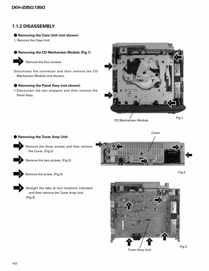
- Removing the Tuner Amp Unit
Remove the three screws and then remove
the Cover. (Fig.2)
Remove the two screws. (Fig.2)
Remove the screw. (Fig.3)
Straight the tabs at fore locations indicated
and then remove the Tuner Amp Unit.
(Fig.3)
- Removing the Case Unit (not shown)
1. Remove the Case Unit.
- Removing the CD Mechanism Module (Fig.1)
Remove the four screws.
Disconnect the connector and then remove the CD
Mechanism Module (not shown).
- Removing the Panel Assy (not shown)
1.Disconnect the two stoppers and then remove the
Panel Assy.
Fig.1
Fig.2
Fig.3Tuner Amp Unit
Cover
CD Mechanism Module
7.1.2 DISASSEMBLY

43
DEH-2350,1350
- Removing the Upper Frame
1. Remove six Springs A, two Springs B and four
Screws.
2. Remove two Tabs situated on rear side of the Upper
Frame, remove two Arms on the front side, then
remove two Tabs on the front side.
- Removing the Carriage Mechanism
1. Disengage the Carriage Mechanism from the two
dampers situated in the front side by driving it up,
then disengage and remove the mechanism from the
one damper by driving it up aslant into front side
direction.
Note : When assembling the Carriage Mechanism, coat
the dampers with alcohol prior to the assembly.
- Removing the Clamp Arm Assy
1. Remove a Spring A, a B and a Spring C.
2. Drive the Clamp Arm Assy up into rear side direction,
then disengage the arm from its current position
Finally, drive the assembly approximately 45 degrees
upward, then slide the assembly toward right side to
remove it.
B
A
B A
A
A
Arm
Arm
A
B
C
Upper Frame
Carriage Mechanism Section
Clamp Arm Assy Section
A
A

44
DEH-2350,1350
- Removing the Guide Arm Assy
1. Remove a connector, a spring A and B
2. Drive the Guide Arm Assy up aslant into rear side
direction, then remove it from a Pin. Finally, drive the
assembly approximately 45 degrees upward, then
slide the assembly toward left side to remove it.
Note : When assembling the guide arm assembly, route
the cord inside the assembly. In this operation,
care must be exercised so that cord may be
caught by the gear.
- Removing the LO Arm Assy
1. Remove two Pins to dismount the LO Arm Assy.
- Removing the Control Unit and the Spindle
Motor
1. Remove from the connector after mounting the short
pin on the flexible PCB of the pickup unit.
2. Remove two Soldered joints, then remove two
Screws A.
3. Remove two connectors and a Screw B.
4. Disengage the Control Unit from two Tabs, then dis-
mount the unit by sliding it toward left.
5. Dismount the Spindle Motor.
A
Guide Arm Assy Section
B
Pin
LO Arm Assy Section
Spindle Motor
A A
Control Unit
Short Pin
B
45
DEH-2350,1350
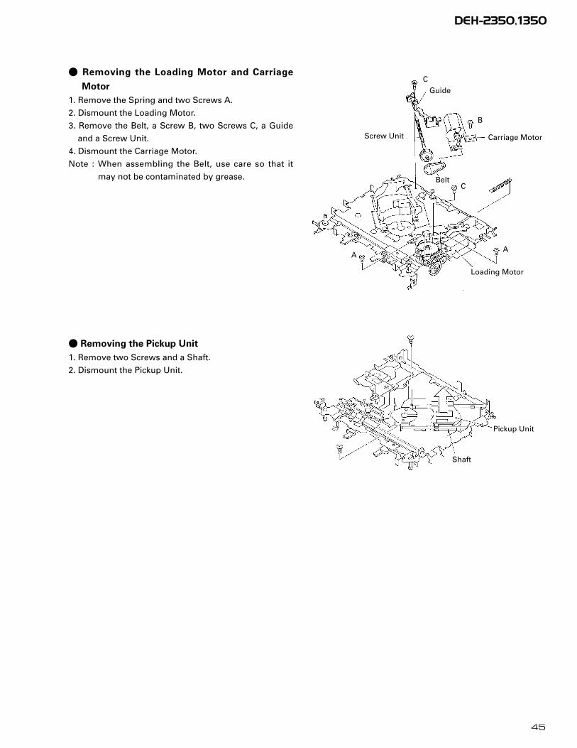
- Removing the Loading Motor and Carriage
Motor
1. Remove the Spring and two Screws A.
2. Dismount the Loading Motor.
3. Remove the Belt, a Screw B, two Screws C, a Guide
and a Screw Unit.
4. Dismount the Carriage Motor.
Note : When assembling the Belt, use care so that it
may not be contaminated by grease.
- Removing the Pickup Unit
1. Remove two Screws and a Shaft.
2. Dismount the Pickup Unit.
Pickup Unit
Shaft
CGuide
B
Screw Unit Carriage Motor
AA
CBelt
Loading Motor
46
DEH-2350,1350
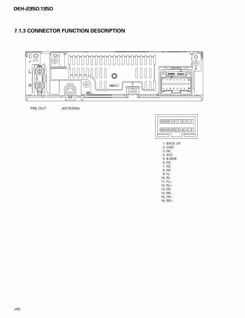
7.1.3 CONNECTOR FUNCTION DESCRIPTION
579 13
468 210121416
111315
1. BACK UP 2. GND 3. NC 4. ACC 5. B.REM 6. NC 7. NC 8. NC 9. FL-10. RL-11. FL+12. RL+13. FR-14. RR-15. FR+16. RR+
PRE OUT ANTENNA

47
DEH-2350,1350
7.2 PARTS
7.2.1 IC
- Pin Functions(PE5196A)Pin No. Pin Name I/O Format Function and Operation
1 MODEL1 I Model select input2 NL1 I Noise level input3 NL2DT I Noise level input 24 AVSS AVSS5 ST I Stereo input6 SD I SD signal input 7 AREF1 AVREF18 KYDT I Key data input9 DPDT O C Key data output
10 SDBW I SDBW input11 TUNPDI I PLL IC data input12 TUNPDO O C PLL IC data output13 TUNPCK O C PLL IC clock output14 TUNPCE O C PLL IC chip enable output15 currq O C Tuner voltage FIX output16 XSI I C CD LSI serial data input(TSI)17 XSO O C CD LSI serial data output(TSO)18 XSCK O C CD LSI serial clock output(TSCK)19 drst O C RDS decoder reset output20 ADPW O C A/D converter power output21 fm/AM O C Tuner power supply control output22 VDCONT O C VD power supply control output23 CONT O C Servo driver power control output24 XAO O C CD LSI command / data control output25 xrst O C CD LSI reset control output26 xstb O C CD LSI strobe output27 CLAMP I Disc clamp sense input28 MIRR I Mirror detection input 29 FOK I Focus OK signal input30 LOCK I Spindle lock detector input31 CDLOAD O LOAD motor loading control output32 TELIN I Cellular mute input33 VSS VSS34 CDEJECT O LOAD motor eject control output35 CD5VON O C CD +5V power supply control output
36–39 NC Not used40 RECIEVE O C RDS decoder receiving output41 swvdd O C Grille microcomputer power supply control output42 SYSPW O C System power supply control output43 ILMPW O C Illumination power output44 mute O C Mute output45 PEE O C Beep tone output46 LOCH O C LOCH output47 RDS57K I 57kHzBP-OUT sense input48 TUNPCE2 O C EEPROM chip enable output49 PCL O C Test mode clock adjustment output50 VCK O C Clock output for electronic volume51 VDT O C Data output for electronic volume52 ANTPW O Antenna power output53 VST O Strobe pulse output for electronic volume54 DALMON O Stand-by output
55,56 NC Not used57 LOCL O LOCL output58 rdslk I RDSLK input
48
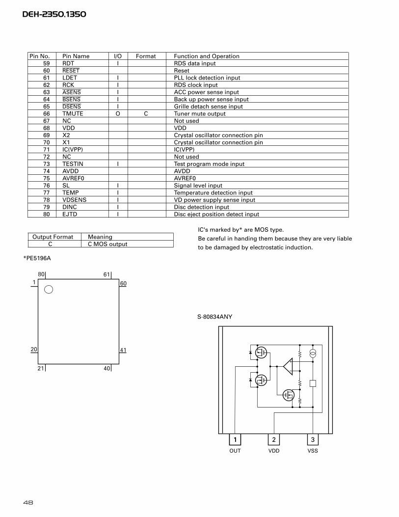
DEH-2350,1350
Pin No. Pin Name I/O Format Function and Operation59 RDT I RDS data input60 reset Reset61 LDET I PLL lock detection input62 RCK I RDS clock input63 asens I ACC power sense input64 bsens I Back up power sense input65 dsens I Grille detach sense input66 TMUTE O C Tuner mute output67 NC Not used68 VDD VDD69 X2 Crystal oscillator connection pin70 X1 Crystal oscillator connection pin71 IC(VPP) IC(VPP)72 NC Not used73 TESTIN I Test program mode input74 AVDD AVDD75 AVREF0 AVREF076 SL I Signal level input77 TEMP I Temperature detection input78 VDSENS I VD power supply sense input79 DINC I Disc detection input80 EJTD I Disc eject position detect input
801
20
21 40
41
60
61
*PE5196A
Output Format MeaningC C MOS output
IC's marked by* are MOS type.
Be careful in handing them because they are very liable
to be damaged by electrostatic induction.
S-80834ANY
1 2 31
OUT VDD VSS
49
DEH-2350,1350
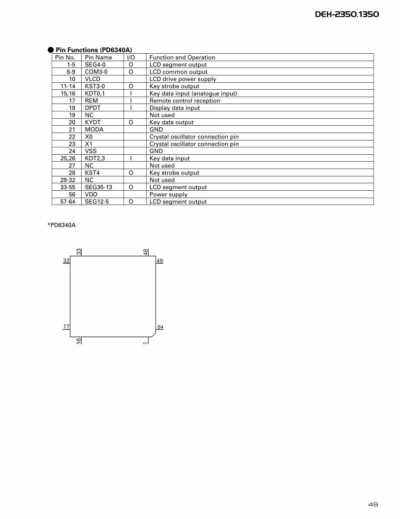
- Pin Functions (PD6340A)Pin No. Pin Name I/O Function and Operation
1-5 SEG4-0 O LCD segment output6-9 COM3-0 O LCD common output 10 VLCD LCD drive power supply
11-14 KST3-0 O Key strobe output15,16 KDT0,1 I Key data input (analogue input)
17 REM I Remote control reception18 DPDT I Display data input19 NC Not used20 KYDT O Key data output21 MODA GND22 X0 Crystal oscillator connection pin23 X1 Crystal oscillator connection pin24 VSS GND
25,26 KDT2,3 I Key data input27 NC Not used28 KST4 O Key strobe output
29-32 NC Not used33-55 SEG35-13 O LCD segment output
56 VDD Power supply57-64 SEG12-5 O LCD segment output
*PD6340A
49
4833
32
17
16 1
64

50
DEH-2350,1350
- Pin Functions (UPD63711GC)Pin No. Pin Name I/O Function and Operation
1 D.GND Logic circuit GND2 RFOK O RFOK signal output3 rst I Reset signal input4 A0 I Command/parameter identification signal input5 stb I Data strobe signal input6 sck I Clock signal input for serial data input/output7 SO O Serial data and status signal output8 SI I Serial data input9 xtalen I Crystal oscillation control pin
10 D.VDD Positive power supply terminal to logic circuit11 DA.VDD Positive power supply terminal to D/A converter12 R_OUT O Right channel audio output signal13 DA.GND D/A converter GND14 REGC I The outside putting capacitor connection pin for SCF regulator15 DA.GND D/A converter GND16 L_OUT O Left channel audio output signal17 DA.VDD Positive power supply terminal to D/A converter18 R+ O Right channel audio data output19 R- O Right channel audio data output20 L- O Left channel audio data output21 L+ O Left channel audio data output22 X.VDD Positive power supply terminal to crystal oscillation circuit23 XTAL I Crystal oscillator connect pin24 xtal O Crystal oscillator connect pin25 X.GND Crystal oscillation circuit GND26 D.VDD Positive power supply terminal to logic circuit27 EMPH O Output pin for the pre-emphasis data in the sub-Q code28 FLAG O Flag output pin to indicate that audio data currently being output consists
of noncorrectable data29 DIN I Serial data input to internal DAC30 DOUT O Serial audio data output31 SCKIN I Serial clock input to internal DAC32 SCKO O Audio data that is output from DOUT changes at rising edge of this clock33 LRCKIN I LRCK signal input to internal DAC34 LRCK O Signals to distinguish the right and left channels of the audio data output
from DOUT35 HOLD O Defect detection output36 TX O Digital audio interface data output37 D.GND Logic circuit GND38 C16M O Oscillator clock buffering output39 LIMIT I Status of the pin is output at Bit 5 of the status output40 D.VDD Positive power supply terminal to logic circuit41 LOCK O EFM synchronous detection signal42 RFCK O Frame synchronous signal of XTAL-system43 MIRR O MIRR output44 PLCK O Monitor pin of bit clock45 D.GND Logic circuit GND46 C1D1 O Output pin for indicating the C1 error correction results47 C1D2 O Output pin for indicating the C1 error correction results48 C2D1 O Output pin for indicating the C2 error correction results49 C2D2 O Output pin for indicating the C2 error correction results50 C2D3 O Output pin for indicating the C2 error correction results51 D.VDD Positive power supply terminal to logic circuit52 PACK O CD-TEXT PACK synchronous signal53 TSO O CD-TEXT data serial output54 TSI I CD-TEXT control parameter serial input55 tsck I CD-TEXT serial clock input56 TSTB I CD-TEXT parameter strobe signal input57 D.GND Logic circuit GND

51
DEH-2350,1350
Pin No. Pin Name I/O Function and Operation58 TEST0 I Test pin59 TEST1 I Test pin60 ATEST O Test pin61 A.GND Analog circuit GND62 FD O Focus drive output63 TD O Tracking drive output64 SD O Sled drive output65 MD O Spindle drive output66 DAC0 O DAC output for adjustment67 DAC1 O DAC output for adjustment68 DAC2 O DAC output for adjustment69 DAC3 O DAC output for adjustment70 A.VDD Positive power supply terminal to analog circuit71 EFM O EFM signal output72 ASY I EFM comparator reference voltage input73 C3T 3T detection capacitor additional pin74 RFI I RF signal input for EFM data regulation75 AGCO O RF signal output of after gain adjustment 76 AGCI I RF-AGC amplifier input77 RFO O RF summing amplifier output78 EQ2 RF amplifier equalizer parts additional pin79 EQ1 RF amplifier equalizer parts additional pin80 RF- I RF summing amplifier inverted input81 A.GND Analog circuit GND82 A I Photo detector A input83 C I Photo detector C input84 B I Photo detector B input85 D I Photo detector D input86 F I Photo detector F input87 E I Photo detector E input88 A.VDD Positive power supply terminal to analog circuit89 REFOUT O Reference electric potential output90 FE- I Focus error amplifier inverted input91 FEO O Focus error amplifier output92 TE- I Tracking error amplifier inverted input93 TEO O Tracking error amplifier output94 TE2 O Tracking error output of after amplification95 TEC I Tracking comparator input96 A.GND Analog circuit GND97 PD I PD detection signal input for LD output monitor 98 LD O LD control current output99 PN I APC circuit control polarity set pin
100 A.VDD Positive power supply terminal to analog circuit
20
21
40
41 60
61
80
1
100
76
26
125
7551
50
*UPD63711GC

52
DEH-2350,1350
1
TAB
2
P-GND2
3
OUT2-
4
STBY
5
OUT2+
6
VCC
7
OUT1-
8
P-GND1
9
OUT1+
10SVR
11IN1
12IN2
13S-GND
14IN4
15IN3
16AC-GND
17OUT3+
18P-GND3
19OUT3-
20VCC
21OUT4+
22MUTE
23OUT4-
24P-GND4
SWITCH
25
+-
+ -
OffsetDetection
+-
+ -
OffsetDetection
+-
+ -
OffsetDetection
+-
+ -
OffsetDetection
Protector;Over current limit
sw_v
cc
stby
Protector;Short circuit
Mute circuit
am
p_v
cc
Stand-byCircuit
Protector;Over voltage
sw_v
ccProtector;Thermal
Reference
1C
M1C
M1C
M1C
M
amp_vcc
PAL006A

53
DEH-2350,1350
No. Symbol I/O Explain1 STIND O stereo "Low" when the FM stereo signals are received.
indicator To be pulled up to the "VDD" at 47kΩ.2 FMSD O FM station "High" when signals are received. To be pulled up to the "VDD" at 47kΩ
detector Meanwhile, 10kΩ should be used when taking diver FIX trigger from hereand "High: 0.9VDD or more" and "Low: 250mV or less".(Should satisfy the diver IC specifications)
3 NL1 O noise level-1 "High" when noise is received. Output for the RDS. GND at 47kΩ //1,800pF.4 NL2 O noise level-2 "High" when noise is received. Output for the RDS. GND at 36kΩ //330pF.5 Rch O R channel FM stereo "R-ch" signal output or AM audio output.
output Add the specified di-emphasis constant. 6 Lch O L channel FM stereo "L-ch" signal output or AM audio output.
output Add the specified di-emphasis constant. 7 WC write control EEPROM write control. Writing permissible at "Low". Normally open. 8 SDBW O SD bandwidth SD bandwidth signal output. For detection of detuning data for the RDS.9 NC Not used
10 VDD power Power supply pin for the digital section.supply D.C. 5V +/- 0.25V. Be careful about overlapping noise in the logic section.
11 DGND digital ground Grounding for the digital section. 12 CE2 I chip enable-2 EEPROM chip enable. Active a "Low"
To be pulled up to the "VDD" at 47kΩ13 SL I/O signal level Received FM/AM signal level (strength) output.
Connect the specified load resistor and capacitor (10k Ω + 39k Ω //4,700pF) 14 DI/DO I/O data input/ Data input/Data output
data output To be pulled up to the "VDD" at 47kΩ15 CK I clock Clock input To be pulled up to the "VDD" at 47kΩ16 CE1 I chip enable-1 AF·RF chip enable. Active at "High" To be grounded at 47kΩ17 NC Not used18 LDET O lock detector Active at "Low". To be pulled up to the "VDD" at 47kΩ19 CREQ I current request Active at "Low". To be grounded at 47kΩ20 NC Not used21 COMP O composite signal FM composite signal output. r out < 100Ω22 VCC power supply Analog section power supply pin.D.C.8.4V +/- 0.3V 23 LOCH I local high FM local high pin. When seeking local high, apply 5V together with "LOCL". 24 FMLOCL I FM local low FM local low pin. When seeking local low, apply 5V to the base of the NPN
transistor with which the specified resistor is being connected to the emitter. Keep it open in case of ordinary marketed models.
25 LOCL I local low FM/AM local low pin. When seeking local low, apply 5V to the base of the NPN transistor. Since this pin is exclusive for AM when the FMLOCL is in use,do not drive it under FM.
26 RFGND RF ground Grounding for the antenna section. 27 FMANT I FM antenna input FM antenna input. 75Ω. Serge absorber (DSP-201M-S00B) is necessary. 28 AMANT I AM antenna input AM antenna input. High impedance.
Connect to the antenna through an L (LAU type) of 4.7µH.To cope with thepower transmission line hums, insert a series circuit consisting of an L(a coil of about 100mH) + R (a resistor of 470 Ω to 2.2kΩ) between the GND.
IC 3EEPROM
FM/AM TUNER UNIT
28
27
FM/AM 1ST IF 10.7MHzT51 Q51 CF51 CF52 CF53
IC1MIXER, IF AMP, DET.
6
21
18LDET
COMP
2225 10 14 12 15 16 8 13 2 3 4
CF202
VDDVCC
DI/D
O
CE
2
CK
CE
1
SD
BW
SL
FMS
D
NL1
NL2
IC 2 FM MPX
AMANT
FMANT
ATT
ATT
AMRF
FMRF
IMG ADJ
RF ADJ
X90110.25MHz
ANT ADJ
LOCL23
LOCH
AMDETMPXREF 41kHz
AM 2ND IF450kHz
19
CR
EQ
11
DG
ND
1
ST
IND
L ch
5R ch
924
NC
FMLO
CL
20177N
C
NC
WC
26 RFGND

54
DEH-2350,1350
SEG37
SEG35
SEG34
SEG33
SEG32
SEG31
SEG30
SEG29
SEG28
SEG27
SEG26
SEG25
SEG24
SEG23
SEG22
SEG21
SEG20
SEG18
SEG17
SEG16
SEG15
SEG14
SEG13
SEG12
SEG11
SEG10
SEG9
SEG8
SEG7
SEG6
SEG5
SEG4
SEG3
SEG2
NC
NC
SEG19
SEG36
COM2B
COM0A
COM2C
COM3B
COM2D
COM1B
COM0B
SEG39
SEG38
COM3A
COM2A
COM1A
37
36
35
34
33
32
31
30
29
28
27
26
25
24
23
22
20
19
18
17
16
15
14
13
12
11
10
9
8
7
6
5
4
3
2
21
1
47
46
45
44
43
42
41
39
38
50
49
48
40
COM2B
COM0A
COM2C
COM3B
COM2D
COM1B
COM0B
COM3A
COM2A
COM1A
SE
GM
EN
T
CO
MM
ON
7.2.2 DISPLAY
- CAW1606(DEH-2350/X1M/ES), CAW1633(DEH-1350/X1M/ES)

DEH-2350,1350
55
7.3 OPERATIONAL FLOW CHART
VDD=5V68pin
Power ON
BSENS=L
ASENS=L
DSENS=L
bsens64pin
asens63pin
dsens65pin
ADPW←H20pin
SWVDD←L41pin
Source keys operative
Completes power-on operation.(After that, proceed to each source operation.)
SYSPW←H42pin
Starts communication with Grille microcomputer.
Source ON
300ms
300ms
In case of the above signal, the communication with Grille microcomputer may fail.If the time interval is not 300msec, the oscillator may be defective.
56
DEH-2350,1350
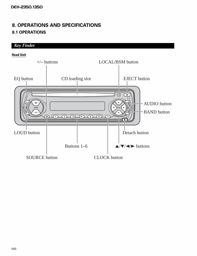
8. OPERATIONS AND SPECIFICATIONS
8.1 OPERATIONS
Key Finder
Buttons 1–6
EJECT buttonCD loading slot
AUDIO button
5/∞/2/3 buttons
SOURCE button
+/– buttons
BAND button
LOCAL/BSM button
Detach button
EQ button
LOUD button
CLOCK button
Head Unit

57
DEH-2350,1350
Bas
ic O
pera
tion
To L
iste
n to
Mus
icT
he f
ollo
win
g ex
plai
ns th
e in
itial
ope
ratio
ns r
equi
red
befo
re y
ou c
an li
sten
to m
usic
.
Not
e:•
Loa
ding
a d
isc
in th
is p
rodu
ct.
1.Se
lect
the
des
ired
sou
rce
(e.g
. Tun
er).
Eac
h pr
ess
of th
e SO
UR
CE
but
ton
sele
cts
the
desi
red
sour
ce in
the
follo
win
g or
der:
Bui
lt-in
CD
pla
yer
=T
uner
Not
e:•
Whe
n no
dis
c is
set
in th
is p
rodu
ct, b
uilt-
in C
D p
laye
r so
urce
will
not
cha
nge.
•W
hen
this
pro
duct
’s b
lue/
whi
te le
ad is
con
nect
ed to
the
car’
s A
uto-
ante
nna
rela
y co
ntro
l ter
min
al,
the
car’
s A
uto-
ante
nna
exte
nds
whe
n th
is p
rodu
ct’s
sou
rce
is s
witc
hed
ON
. To
retr
act t
he a
nten
na,
switc
h th
e so
urce
OFF
.
2.R
aise
or
low
er t
he v
olum
e.
3.Tu
rn t
he s
ourc
e O
FF.
Hol
d fo
r 1
seco
nd
Eac
h pr
ess
chan
ges
the
Sour
ce ..
.
Bas
ic O
pera
tion
of T
uner
R
eset
the
AM
tuni
ng s
tep
from
9 k
Hz
(the
fac
tory
pre
set s
tep)
to 1
0 kH
z w
hen
usin
g th
etu
ner
in N
orth
, Cen
tral
or
Sout
h A
mer
ica.
Pres
et N
umbe
r Ind
icat
orB
and
Indi
cato
r
Freq
uenc
y In
dica
tor
Man
ual a
nd S
eek
Tuni
ng
•Y
ou c
an s
elec
t th
e tu
ning
met
hod
by c
hang
ing
the
leng
th o
f ti
me
you
pres
s th
e 2
/3bu
tton
.
Man
ual T
unin
g (s
tep
by s
tep)
0.5
seco
nds
or le
ss
Seek
Tun
ing
0.5
seco
nds
or m
ore
Not
e:•
If y
ou c
ontin
ue p
ress
ing
the
butto
n fo
r lo
nger
than
0.5
sec
onds
, you
can
ski
p br
oadc
ast
stat
ions
. See
k T
unin
g st
arts
as
soon
as
you
rele
ase
the
butto
n.•
Ster
eo in
dica
tor
“”
light
s w
hen
a st
ereo
sta
tion
is s
elec
ted.
Pres
et T
unin
g
•Y
ou c
an m
emor
ize
broa
dcas
t st
atio
ns in
but
tons
1th
roug
h 6
for
easy
, one
-tou
ch s
tati
on r
ecal
l.
Pres
et s
tatio
n re
call
2 se
cond
s or
less
Bro
adca
st s
tatio
n pr
eset
mem
ory
2 se
cond
s or
mor
e
Not
e:•
Up
to 1
8 FM
sta
tions
(6
in F
M1,
FM
2 an
d FM
3) a
nd 6
AM
sta
tions
can
be s
tore
d in
mem
ory.
•Y
ou c
an a
lso
use
the
5or
∞bu
ttons
to r
ecal
l bro
adca
st s
tatio
nsm
emor
ized
in b
utto
ns 1
thro
ugh
6.
Ban
d FM1
=FM
2=
FM3
=A
M

58
DEH-2350,1350
Bas
ic O
pera
tion
of B
uilt-
in C
D P
laye
r
Trac
k N
umbe
r Ind
icat
orPl
ay T
ime
Indi
cato
r
Ejec
t Not
e:•
The
CD
fun
ctio
n ca
n be
turn
ed O
N/O
FFw
ith th
e di
sc r
emai
ning
in th
is p
rodu
ct.
• A
dis
c le
ft p
artia
lly in
sert
ed a
fter
eje
ctio
nm
ay in
cur
dam
age
or f
all o
ut.
CD L
oadi
ng S
lot
Not
e:•
The
bui
lt-in
CD
pla
yer
play
s on
e st
anda
rd 1
2 cm
or 8
cm
(si
ngle
) C
D a
t a ti
me.
Do
not u
se a
nad
apte
r w
hen
play
ing
8 cm
CD
.•
Don
’t in
sert
any
mat
eria
ls e
xcep
t for
CD
into
CD
load
ing
slot
.
Trac
k Se
arch
and
Fas
t For
war
d/Re
vers
e
•Y
ou c
an s
elec
t be
twee
n T
rack
Sea
rch
or F
ast
For
war
d/R
ever
se b
y pr
ess-
ing
the
2/3
butt
on fo
r a
diff
eren
t le
ngth
of
tim
e.
Tra
ck S
earc
h0.
5 se
cond
s or
less
Fast
For
war
d/R
ever
se
Con
tinue
pre
ssin
g
Not
e:•
If a
dis
c ca
nnot
be
inse
rted
ful
ly o
r pl
ayba
ck f
ails
, mak
e su
re th
e re
cord
ed s
ide
is d
own.
Push
the
EJE
CT
but
ton
and
chec
k th
e di
sc f
or d
amag
e be
fore
rei
nser
ting
it.•
If a
dis
c is
inse
rted
with
the
reco
rded
sid
e up
, it w
ill b
e ej
ecte
d au
tom
atic
ally
aft
er a
few
mom
ents
.•
If th
e bu
ilt-i
n C
D p
laye
r ca
nnot
ope
rate
pro
perl
y, a
n er
ror
mes
sage
(su
ch a
s “E
RR
-14”
)ap
pear
s on
the
disp
lay.
Ref
er to
“B
uilt-
in C
D P
laye
r’s
Err
or M
essa
ge”.
Bas
ic O
pera
tion
59
DEH-2350,1350
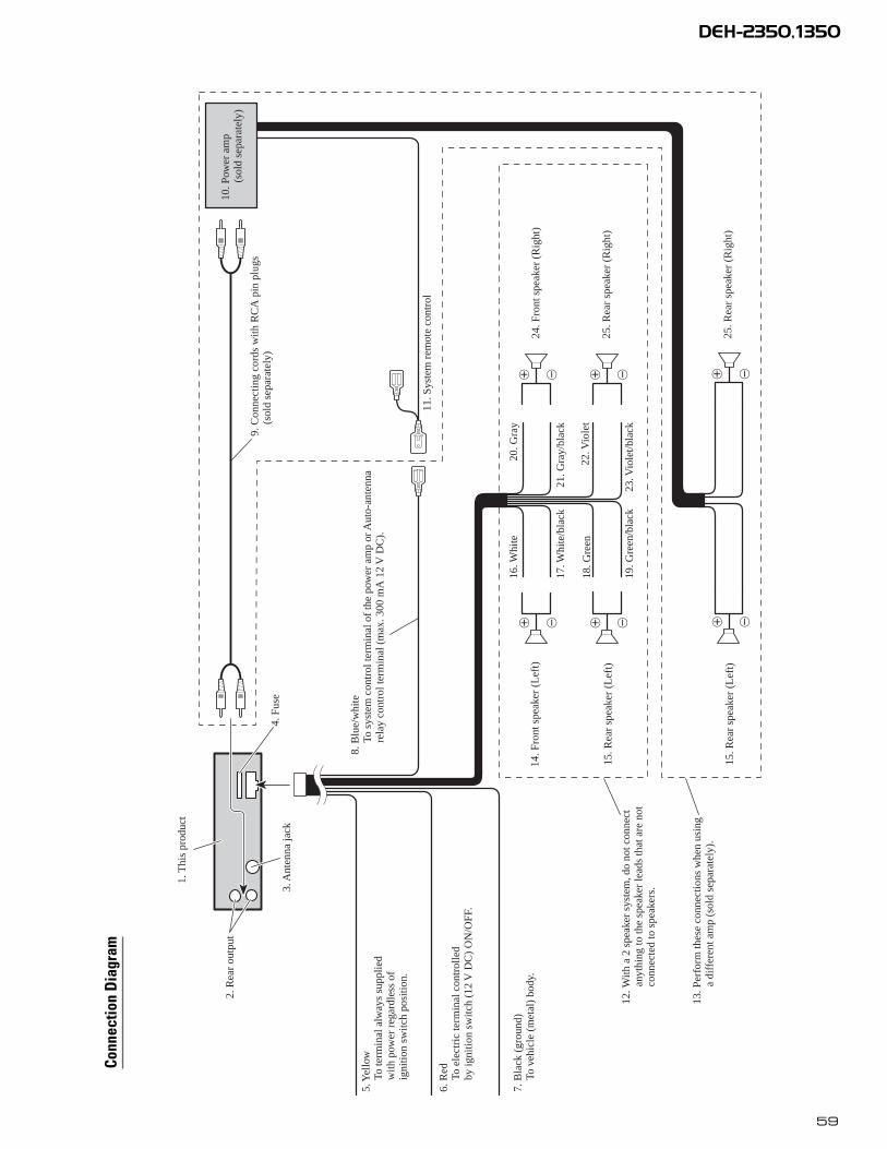
+ ≠
+ ≠
+ ≠
+ ≠
+ ≠
+ ≠
8.B
lue/
whi
teTo
syst
emco
ntro
lter
min
alof
the
pow
eram
por
Aut
o-an
tenn
are
lay
cont
rolt
erm
inal
(max
.300
mA
12V
DC
).
9.C
onne
ctin
gco
rds
with
RC
Api
npl
ugs
(sol
dse
para
tely
)
11.S
yste
mre
mot
eco
ntro
l
24.F
ront
spea
ker
(Rig
ht)
25.R
ear
spea
ker
(Rig
ht)
16.W
hite
20.G
ray
17.W
hite
/bla
ck
18.G
reen
19.G
reen
/bla
ck
21.G
ray/
blac
k
22.V
iole
t
23.V
iole
t/bla
ck
14.F
ront
spea
ker
(Lef
t)
15.R
ear
spea
ker
(Lef
t)
13.P
erfo
rmth
ese
conn
ectio
nsw
hen
usin
ga
diff
eren
tam
p(s
old
sepa
rate
ly).
12.W
itha
2sp
eake
rsy
stem
,do
notc
onne
ctan
ythi
ngto
the
spea
ker
lead
sth
atar
eno
tco
nnec
ted
tosp
eake
rs.
2.R
ear
outp
ut
1.T
his
prod
uct
3.A
nten
naja
ck4.
Fuse
5.Y
ello
wTo
term
inal
alw
ays
supp
lied
with
pow
erre
gard
less
ofig
nitio
nsw
itch
posi
tion.
7.B
lack
(gro
und)
Tove
hicl
e(m
etal
)bo
dy.
6.R
edTo
elec
tric
term
inal
cont
rolle
dby
igni
tion
switc
h(1
2V
DC
)O
N/O
FF.
10.P
ower
amp
(sol
dse
para
tely
)
15.R
ear
spea
ker
(Lef
t)25
.Rea
rsp
eake
r(R
ight
)
Conn
ectio
n D
iagr
am

DEH-2350,1350
8.2 SPECIFICATIONS
GeneralPower source .......... 14.4 V DC (10.8 – 15.1 V allowable)Grounding system ........................................ Negative typeMax. current consumption ...................................... 10.0 ADimensions
(DIN) (chassis) ...... 178 (W) × 50 (H) × 159 (D) mm(nose) ............ 188 (W) × 58 (H) × 19 (D) mm
(D) (chassis) ...... 178 (W) × 50 (H) × 164 (D) mm(nose) ............ 170 (W) × 48 (H) × 14 (D) mm
Weight ...................................................................... 1.4 kgElectrode dark current .................................... 6mA or less
AmplifierContinuous power output is 22 W per channel min. into 4ohms, both channels driven 50 to 15,000 Hz with no morethan 5% THD. (DEH-2350)
Continuous power output is 20 W per channel min. into 4ohms, both channels driven 50 to 15,000 Hz with no morethan 5% THD. (DEH-1350)
Maximum power output(DEH-2350).................................................. 50 W × 4(DEH-1350).................................................. 45 W × 4
Load impedance .......................... 4 Ω (4 – 8 Ω allowable)Preout maximum output
level/output impedance ............................ 2.2 V/1 kΩEqualizer (3-Band Equalizer)
(Low) .................................................. Level: ±12 dB(Mid) .................................................... Level: ±12 dB(High) .................................................. Level: ±12 dB
Loudness contour(Low) .................. +3.5 dB (100 Hz), +3 dB (10 kHz)(Mid) ................ +10 dB (100 Hz), +6.5 dB (10 kHz)(High) ................ +11 dB (100 Hz), +11 dB (10 kHz)
(volume: –30 dB)
CD playerSystem .................................... Compact disc audio systemUsable discs .................................................. Compact discSignal format .................... Sampling frequency: 44.1 kHz
Number of quantization bits: 16; linearFrequency characteristics .............. 5 – 20,000 Hz (±1 dB)Signal-to-noise ratio ...... 94 dB (1 kHz) (IEC-A network)Dynamic range ............................................ 92 dB (1 kHz)Number of channels ............................................ 2 (stereo)
FM tunerFrequency range ...................................... 87.5 – 108 MHzUsable sensitivity ...................................................... 9 dBf
(0.8 µV/75 Ω, mono, S/N: 30 dB)50 dB quieting sensitivity .... 15 dBf (1.5 µV/75 Ω, mono)Signal-to-noise ratio ...................... 70 dB (IEC-A network)Distortion .......................... 0.3% (at 65 dBf, 1 kHz, stereo)Frequency response ...................... 30 – 15,000 Hz (±3 dB)Stereo separation .......................... 40 dB (at 65 dBf, 1 kHz)
AM tunerFrequency range ........................ 531 – 1,602 kHz (9 kHz)
530 – 1,640 kHz (10 kHz)Usable sensitivity .............................. 18 µV (S/N: 20 dB)Selectivity .................................................. 50 dB (±9 kHz)
50 dB (±10 kHz)
Note:• Specifications and the design are subject to possi-
ble modification without notice due to improve-ments.
Recommended