1
Chapter 3Top-Level View of System Function and Interconnection
Computer Organization and Architecture Computer Components
• Von Neumann Architecture— Data and Instructions stored in single r/w memory— Contents of memory addressable by location,
regardless of type of data— Sequential execution in memory unless explicitly
modified (e.g., jump, call, or branch instruction)
• It is also possible to construct a computer that executes a single program built into the logic hardware – “hardwired”
Program Concept• Hardwired systems are
inflexible• General purpose
hardware can do different tasks, given correct control signals
• Instead of re-wiring, supply a new set of control signals
What is a program?• A sequence of steps• For each step, an
arithmetic or logical operation is done
• For each operation, a different set of control signals is needed
• Also need temp storage (memory) and way to get input and output
Function of Control Unit
• For each operation a unique code is provided— e.g. ADD, MOVE
• A hardware segment accepts the code and issues the control signals
• We have a computer!
Components
• The Control Unit and the Arithmetic and Logic Unit constitute the Central Processing Unit
• Data and instructions need to get into the system and results out— Input/output
• Temporary storage of code and results is needed— Main memory
2
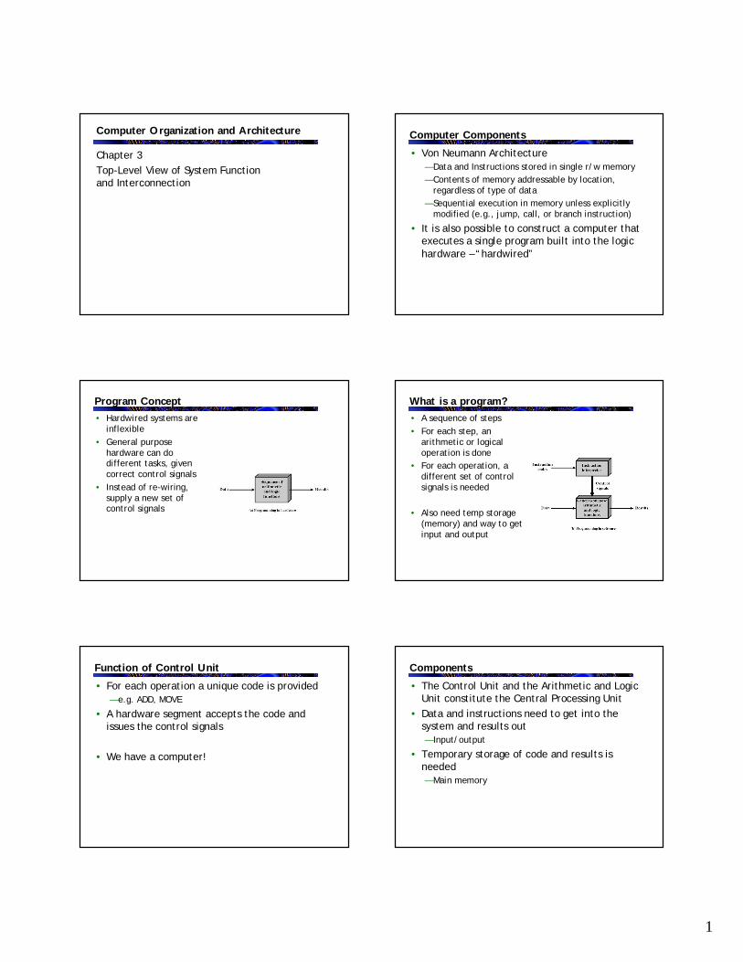
Computer Components:Top Level View Instruction Cycle
• Two steps:— Fetch— Execute
Fetch Cycle
• Program Counter (PC) holds address of next instruction to fetch
• Processor fetches instruction from memory location pointed to by PC
• Increment PC— Unless told otherwise
• Instruction loaded into Instruction Register (IR)• Processor interprets instruction and performs
required actions
Execute Cycle
• Four categories of actions1. Processor-memory
— data transfer between CPU and main memory2. Processor I/O
— Data transfer between CPU and I/O module3. Data processing
— Some arithmetic or logical operation on data4. Control
— Alteration of sequence of operations— e.g. jump
• Instruction execution may involve a combination of these
A Hypothetical Machine Example of Program Execution
3
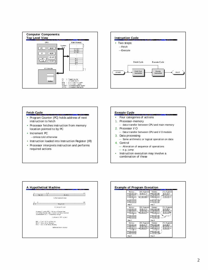
Instruction Cycle State Diagram Interrupts
• Mechanism by which other modules (e.g. I/O) may interrupt normal sequence of processing
• Program/CPU— e.g. overflow, division by zero
• Timer— Generated by internal processor timer— Used in pre-emptive multi-tasking
• I/O— from I/O controller
• Hardware failure— e.g. memory parity error
Software Interrupts
• Some processors support “Software Interrupts”— In particular, both the Intel x86 family that we will use
for assembler and the ARM family use them extensively
• Software interrupts are not really interrupts at all.
• A software interrupt is a machine instruction that causes a transfer of control through the same mechanism used by true interrupts
• Typically used for low-level calls to the operating system or components such as device drivers
Why use interrupts?
• I/O Interrupts are used to improve CPU utilization
• Most I/O devices are relatively slow compared to the CPU
• Human interface devices and printers are especially slow— Keyboard: at best still fewer than 10 keystrokes per
second— Printer: sending a single byte with the value 12
decimal causes a page eject (several seconds)
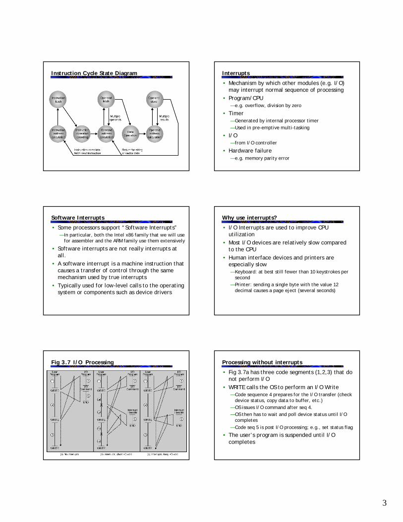
Fig 3.7 I/O Processing Processing without interrupts
• Fig 3.7a has three code segments (1,2,3) that do not perform I/O
• WRITE calls the OS to perform an I/O Write— Code sequence 4 prepares for the I/O transfer (check
device status, copy data to buffer, etc.)— OS issues I/O command after seq 4. — OS then has to wait and poll device status until I/O
completes— Code seq 5 is post I/O processing; e.g., set status flag
• The user’s program is suspended until I/O completes
4
Processing with interrupts
• Fig 3.7b shows processing with interrupts• The WRITE call again transfers control to OS• After write preparation in block 4, control returns
to user program— I/O proceeds concurrently with user program
• When I/O completes, device issues an interrupt request
• OS interrupts user program (marked with *) and executes post I/O code in block 5
Interrupt Cycle
• Added to instruction cycle• Processor checks for interrupt
— Indicated by an interrupt signal
• If no interrupt, fetch next instruction• If interrupt pending:
— Suspend execution of current program — Save context— Set PC to start address of interrupt handler routine— Process interrupt— Restore context and continue interrupted program
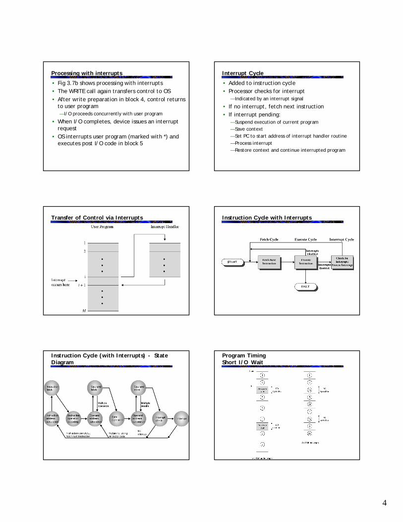
Transfer of Control via Interrupts Instruction Cycle with Interrupts
Instruction Cycle (with Interrupts) - State Diagram
Program TimingShort I/O Wait
5
Long I/O waits
• Fig 3.7c illustrates that processor utilization may not be optimal with long I/O waits
• The program cannot proceed with the second WRITE request until the first has completed
Program Timing: Long I/O Wait
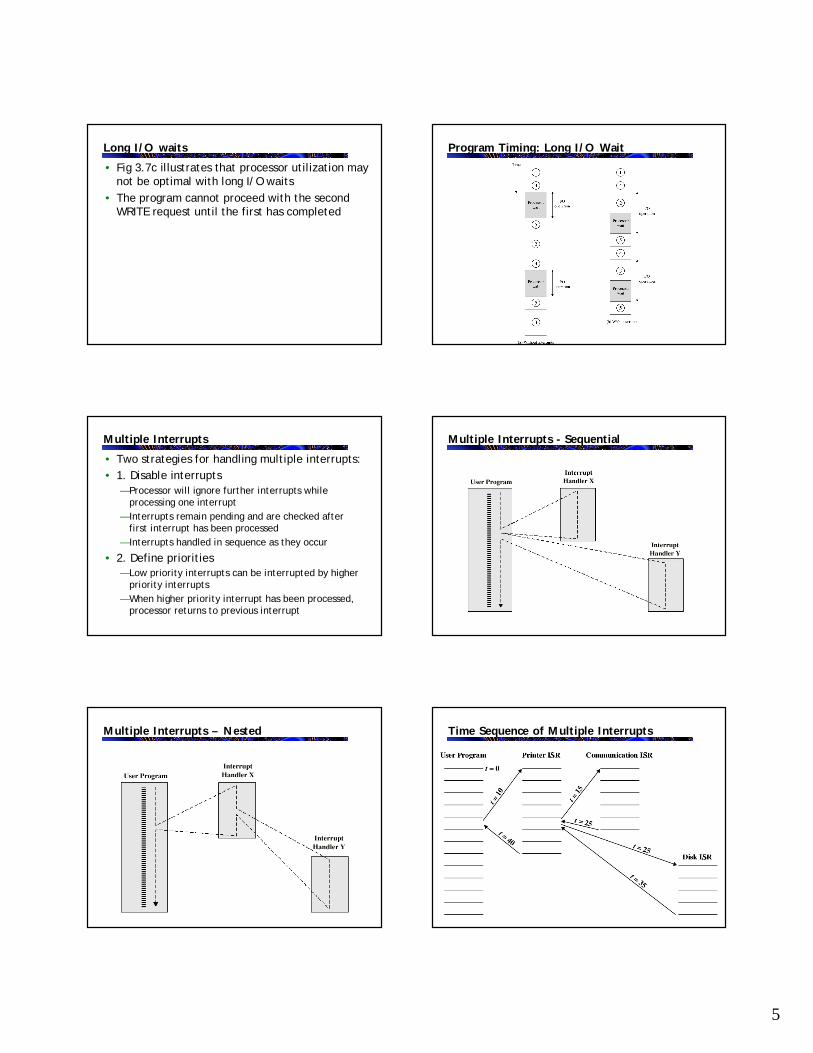
Multiple Interrupts
• Two strategies for handling multiple interrupts:• 1. Disable interrupts
— Processor will ignore further interrupts while processing one interrupt
— Interrupts remain pending and are checked after first interrupt has been processed
— Interrupts handled in sequence as they occur
• 2. Define priorities— Low priority interrupts can be interrupted by higher
priority interrupts— When higher priority interrupt has been processed,
processor returns to previous interrupt
Multiple Interrupts - Sequential
Multiple Interrupts – Nested Time Sequence of Multiple Interrupts
6
I/O Function
• An I/O device (e.g., disk controller) can exchange data directly with the processor
• Just as the processor can read data from memory and write data to memory, it can also read data from I/O devices and write data to I/O devices
Direct Memory Access (DMA)
• In some cases it may be desirable to allow I/O devices to exchange data directly with memory
• The processor will “grant permission” for this exchange to take place
• Processor can then proceed to other work (provided that it does not use the bus granted to the I/O device)
• This operation is called Direct Memory Access (DMA)
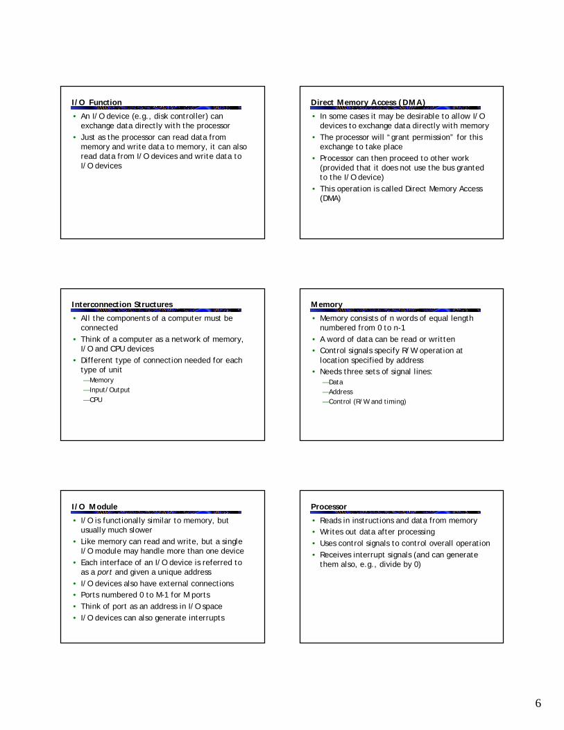
Interconnection Structures
• All the components of a computer must be connected
• Think of a computer as a network of memory, I/O and CPU devices
• Different type of connection needed for each type of unit— Memory— Input/Output— CPU
Memory
• Memory consists of n words of equal length numbered from 0 to n-1
• A word of data can be read or written • Control signals specify R/W operation at
location specified by address• Needs three sets of signal lines:
— Data— Address— Control (R/W and timing)
I/O Module
• I/O is functionally similar to memory, but usually much slower
• Like memory can read and write, but a single I/O module may handle more than one device
• Each interface of an I/O device is referred to as a port and given a unique address
• I/O devices also have external connections• Ports numbered 0 to M-1 for M ports• Think of port as an address in I/O space • I/O devices can also generate interrupts
Processor
• Reads in instructions and data from memory• Writes out data after processing• Uses control signals to control overall operation• Receives interrupt signals (and can generate
them also, e.g., divide by 0)
7
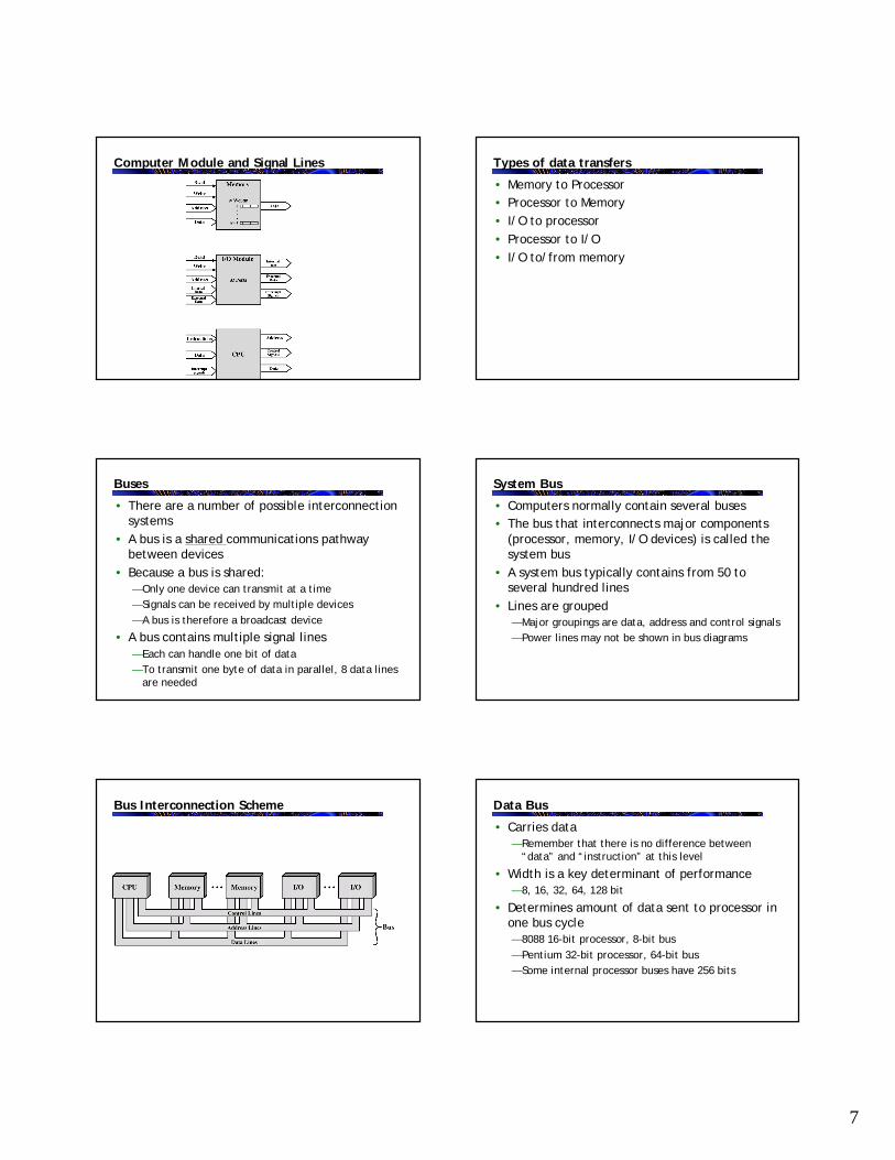
Computer Module and Signal Lines Types of data transfers
• Memory to Processor• Processor to Memory• I/O to processor • Processor to I/O • I/O to/from memory
Buses
• There are a number of possible interconnection systems
• A bus is a shared communications pathway between devices
• Because a bus is shared:— Only one device can transmit at a time— Signals can be received by multiple devices— A bus is therefore a broadcast device
• A bus contains multiple signal lines— Each can handle one bit of data— To transmit one byte of data in parallel, 8 data lines
are needed
System Bus
• Computers normally contain several buses• The bus that interconnects major components
(processor, memory, I/O devices) is called the system bus
• A system bus typically contains from 50 to several hundred lines
• Lines are grouped— Major groupings are data, address and control signals— Power lines may not be shown in bus diagrams
Bus Interconnection Scheme Data Bus
• Carries data— Remember that there is no difference between
“data” and “instruction” at this level
• Width is a key determinant of performance— 8, 16, 32, 64, 128 bit
• Determines amount of data sent to processor in one bus cycle— 8088 16-bit processor, 8-bit bus— Pentium 32-bit processor, 64-bit bus— Some internal processor buses have 256 bits
8
Address bus
• Identify the source or destination of data• e.g. CPU needs to read an instruction (data)
from a given location in memory• Bus width determines maximum memory
capacity of system— e.g. 8080 has 16 bit address bus giving 64k address
space— N bus lines can address 2n words (usually bytes) of
memory
Control Bus
• Transmits control and timing information • Timing signals indicate when bus lines are valid • Control signals specify operations to be
performed
Typical Control Signals
• Memory read/write signals• I/O read/write signals• Bus request/grant • Transfer ACK (acknowledgement)
— Indicates that have been accepted from or placed on bus
• Interrupt Request/ACK• Clock signals synchronize operations• Reset: initializes all modules
Basic Bus Operation
• Module that wishes to send data must— Obtain use of the bus— Then transfer data
• Module that requests data from another module must— Obtain use of the bus— Transfer request to other module over bus— Wait for data to be written to the bus
Big and Yellow?
• What do buses look like?— Parallel lines on circuit boards— Ribbon cables— Strip connectors on mother boards
– e.g. PCI
— Sets of wires
• With VLSI, many components (such as L1 cache) are on the same chip as the processor
• An on-chip bus connects these components
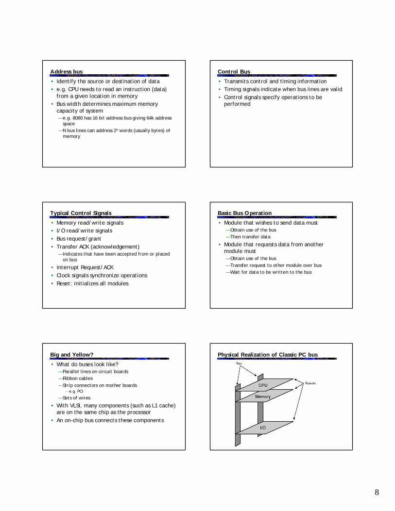
Physical Realization of Classic PC bus
9
Single Bus Problems
• Lots of devices on one bus leads to:— Propagation delays
– Long data paths mean that co-ordination of bus use can adversely affect performance
— Bottlenecks when aggregate data transfer approaches bus capacity
• Most systems use multiple buses to overcome these problems— Hierarchical structure— High-speed limited access buses close to the
processor— Slower-speed general access buses farther away
from the processor
Bus can be a bottleneck
• Can increase data rates and bus width, but peripheral data rates are increasing rapidly— Video and graphics controllers— Network interfaces (1GB ethernet)— High speed storage devices
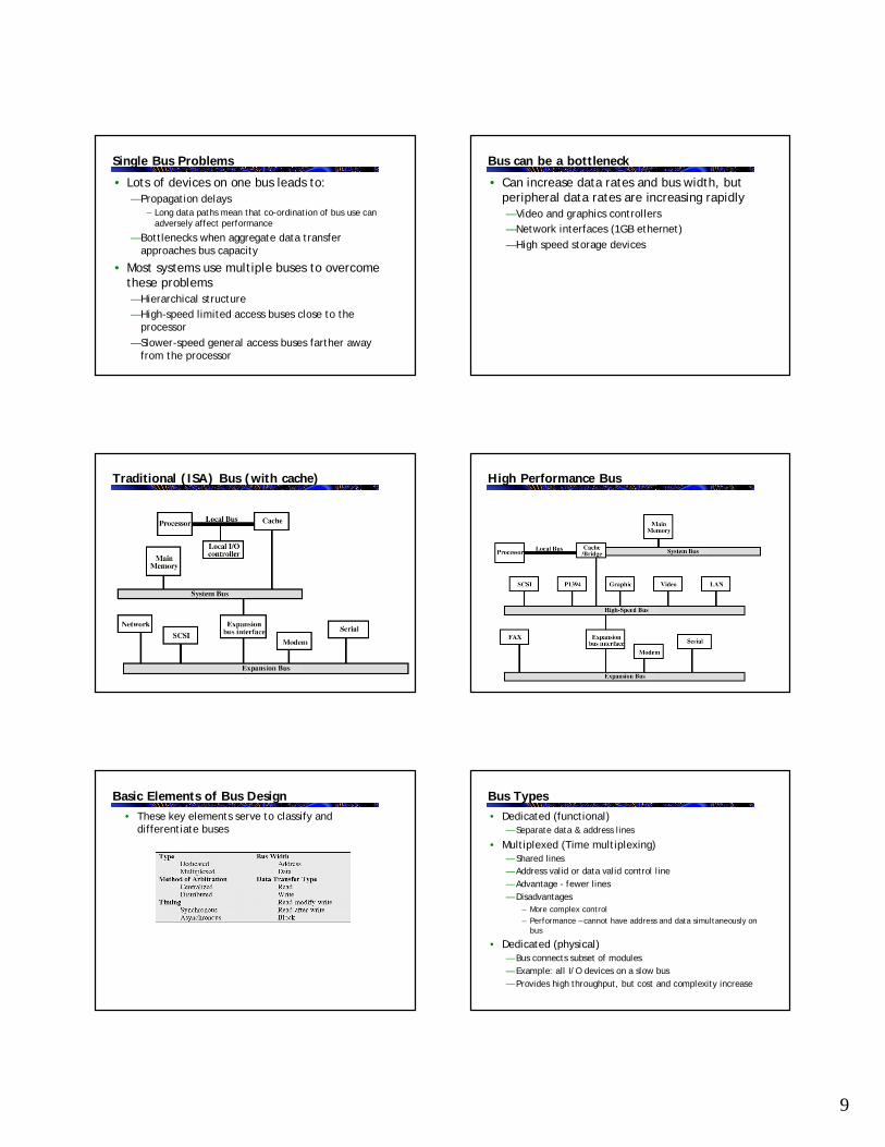
Traditional (ISA) Bus (with cache) High Performance Bus
Basic Elements of Bus Design• These key elements serve to classify and
differentiate buses
Bus Types• Dedicated (functional)
— Separate data & address lines
• Multiplexed (Time multiplexing)— Shared lines— Address valid or data valid control line— Advantage - fewer lines— Disadvantages
– More complex control– Performance – cannot have address and data simultaneously on
bus
• Dedicated (physical)— Bus connects subset of modules — Example: all I/O devices on a slow bus— Provides high throughput, but cost and complexity increase
10
Bus Arbitration
• More than one module controlling the bus• e.g. CPU and DMA controller• Only one module may control bus at one time• Arbitration may be centralised or distributed
Centralised or Distributed Arbitration
• Centralised— Single hardware device controlling bus access
– Bus Controller or Arbiter
— May be part of CPU or separate device
• Distributed— Each module may claim the bus— Control logic on all modules— Module currently controlling bus is the master— Master initiates data transfer with slave device
Timing
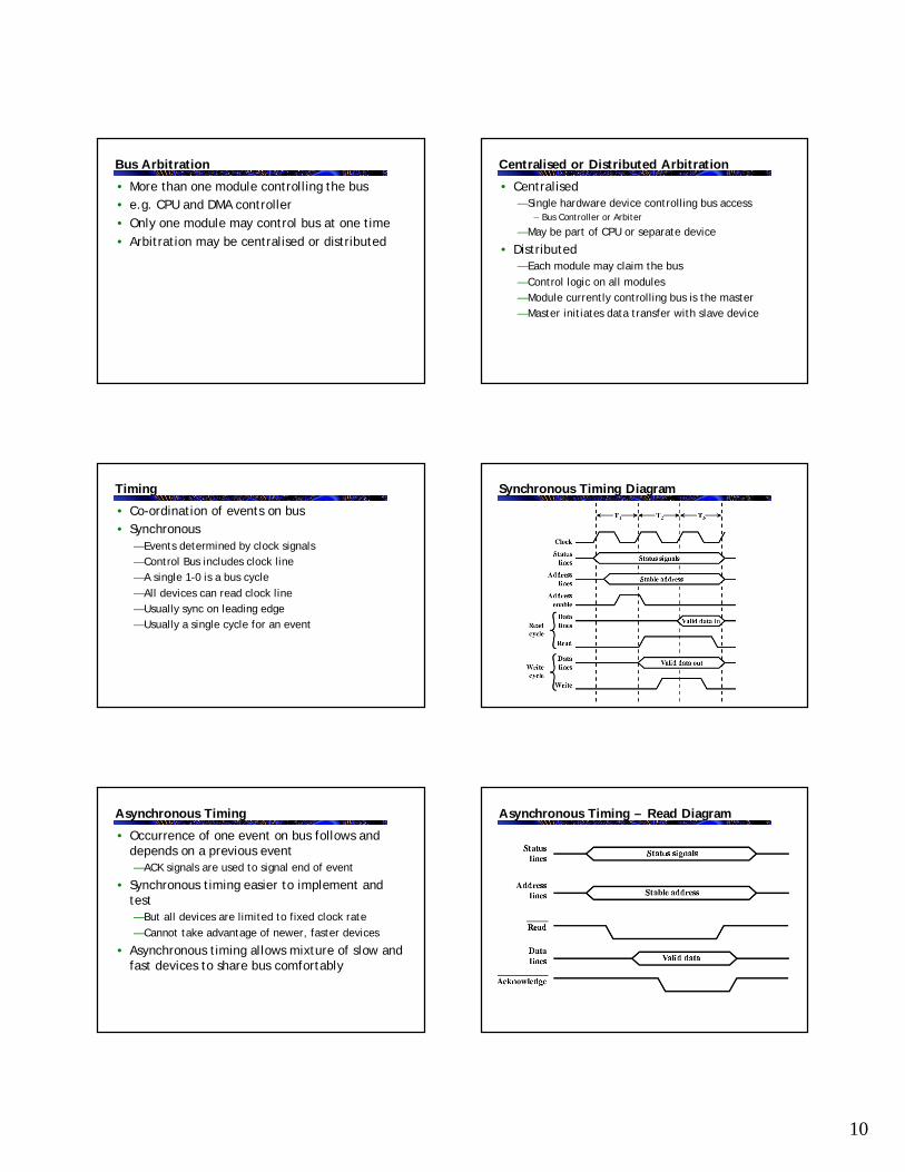
• Co-ordination of events on bus• Synchronous
— Events determined by clock signals— Control Bus includes clock line— A single 1-0 is a bus cycle— All devices can read clock line— Usually sync on leading edge— Usually a single cycle for an event
Synchronous Timing Diagram
Asynchronous Timing
• Occurrence of one event on bus follows and depends on a previous event — ACK signals are used to signal end of event
• Synchronous timing easier to implement and test— But all devices are limited to fixed clock rate— Cannot take advantage of newer, faster devices
• Asynchronous timing allows mixture of slow and fast devices to share bus comfortably
Asynchronous Timing – Read Diagram
11
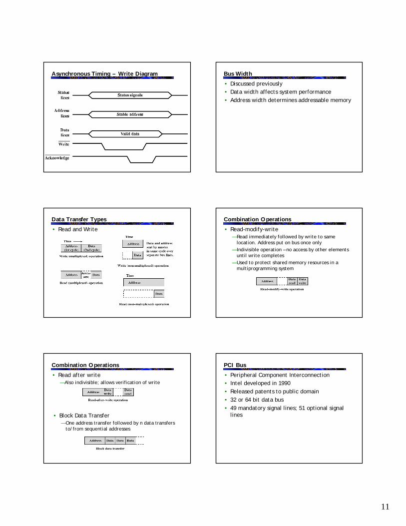
Asynchronous Timing – Write Diagram Bus Width
• Discussed previously• Data width affects system performance• Address width determines addressable memory
Data Transfer Types
• Read and Write
Combination Operations
• Read-modify-write— Read immediately followed by write to same
location. Address put on bus once only— Indivisible operation – no access by other elements
until write completes— Used to protect shared memory resources in a
multiprogramming system
Combination Operations
• Read after write— Also indivisible; allows verification of write
• Block Data Transfer— One address transfer followed by n data transfers
to/from sequential addresses
PCI Bus
• Peripheral Component Interconnection• Intel developed in 1990• Released patents to public domain• 32 or 64 bit data bus• 49 mandatory signal lines; 51 optional signal
lines
12
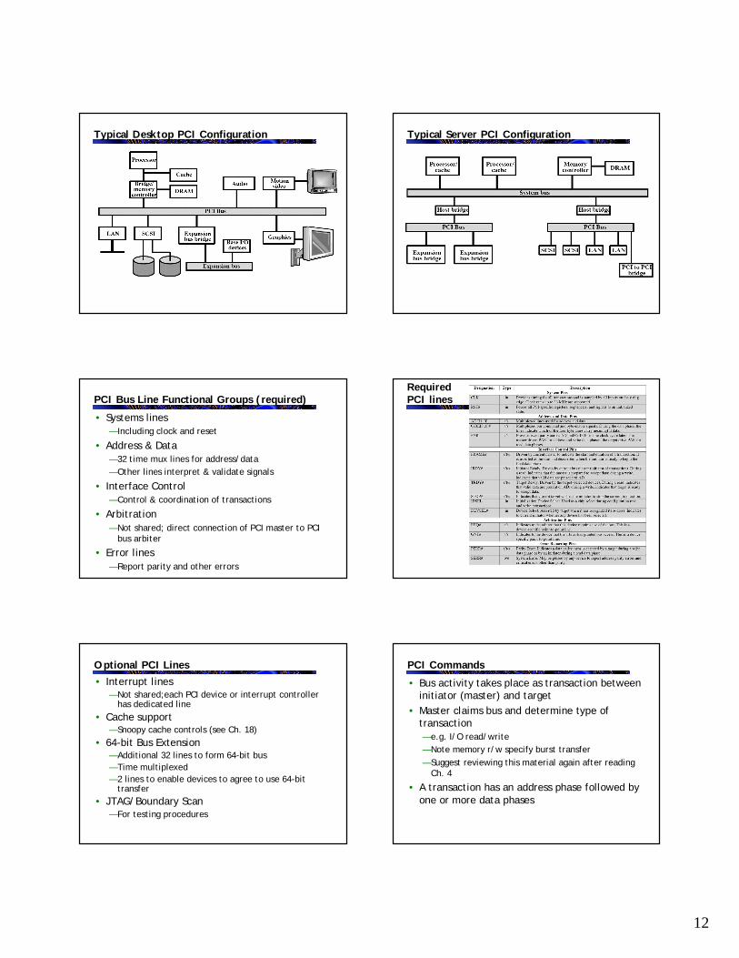
Typical Desktop PCI Configuration Typical Server PCI Configuration
PCI Bus Line Functional Groups (required)
• Systems lines— Including clock and reset
• Address & Data— 32 time mux lines for address/data— Other lines interpret & validate signals
• Interface Control— Control & coordination of transactions
• Arbitration— Not shared; direct connection of PCI master to PCI
bus arbiter
• Error lines— Report parity and other errors
Required PCI lines
Optional PCI Lines
• Interrupt lines— Not shared;each PCI device or interrupt controller
has dedicated line• Cache support
— Snoopy cache controls (see Ch. 18)• 64-bit Bus Extension
— Additional 32 lines to form 64-bit bus— Time multiplexed— 2 lines to enable devices to agree to use 64-bit
transfer• JTAG/Boundary Scan
— For testing procedures
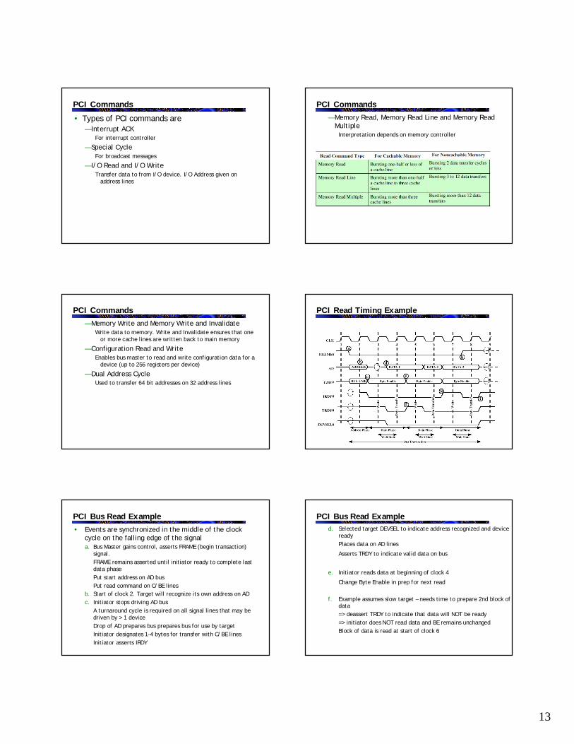
PCI Commands
• Bus activity takes place as transaction between initiator (master) and target
• Master claims bus and determine type of transaction— e.g. I/O read/write— Note memory r/w specify burst transfer— Suggest reviewing this material again after reading
Ch. 4
• A transaction has an address phase followed by one or more data phases
13
PCI Commands
• Types of PCI commands are— Interrupt ACK
For interrupt controller
— Special CycleFor broadcast messages
— I/O Read and I/O WriteTransfer data to from I/O device. I/O Address given on
address lines
PCI Commands— Memory Read, Memory Read Line and Memory Read
MultipleInterpretation depends on memory controller
PCI Commands— Memory Write and Memory Write and Invalidate
Write data to memory. Write and Invalidate ensures that one or more cache lines are written back to main memory
— Configuration Read and WriteEnables bus master to read and write configuration data for a
device (up to 256 registers per device)
— Dual Address CycleUsed to transfer 64 bit addresses on 32 address lines
PCI Read Timing Example
PCI Bus Read Example• Events are synchronized in the middle of the clock
cycle on the falling edge of the signala. Bus Master gains control, asserts FRAME (begin transaction)
signal. FRAME remains asserted until initiator ready to complete last data phasePut start address on AD busPut read command on C/BE lines
b. Start of clock 2. Target will recognize its own address on ADc. Initiator stops driving AD bus
A turnaround cycle is required on all signal lines that may be driven by > 1 deviceDrop of AD prepares bus prepares bus for use by targetInitiator designates 1-4 bytes for transfer with C/BE linesInitiator asserts IRDY
PCI Bus Read Exampled. Selected target DEVSEL to indicate address recognized and device
ready Places data on AD lines
Asserts TRDY to indicate valid data on bus
e. Initiator reads data at beginning of clock 4
Change Byte Enable in prep for next read
f. Example assumes slow target – needs time to prepare 2nd block of data=> deassert TRDY to indicate that data will NOT be ready => initiator does NOT read data and BE remains unchanged Block of data is read at start of clock 6
14
PCI Bus Read Exampleg. During clock 6, target places item 3 on bus, but initiator has
buffer full=> deassert IRDY
=> Target maintains data on bus for extra clock
h. Initiator knows third transfer is last => Deassert FRAME and assert IRDY to complete transfer
i. Initiator deasserts IRDY; bus -> idle state, target deasserts TRDY and DEVSEL
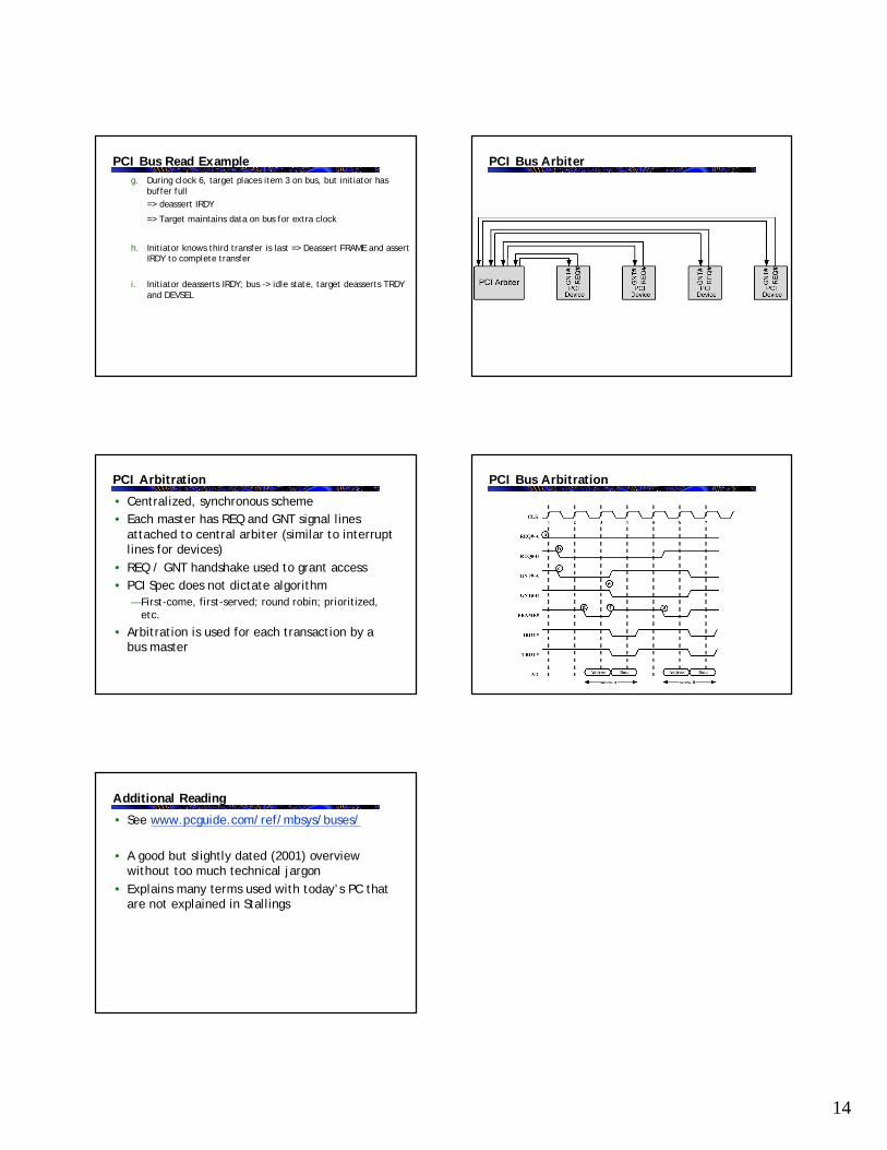
PCI Bus Arbiter
PCI Arbitration
• Centralized, synchronous scheme• Each master has REQ and GNT signal lines
attached to central arbiter (similar to interrupt lines for devices)
• REQ / GNT handshake used to grant access• PCI Spec does not dictate algorithm
— First-come, first-served; round robin; prioritized, etc.
• Arbitration is used for each transaction by a bus master
PCI Bus Arbitration
Additional Reading
• See www.pcguide.com/ref/mbsys/buses/
• A good but slightly dated (2001) overview without too much technical jargon
• Explains many terms used with today’s PC that are not explained in Stallings
Recommended