Colloidal Cerium Oxide Nanoparticles: Synthesis and Characterization Techniques
Jamie C. Clinton Thesis submitted to Virginia Polytechnic Institute and State University
Master of Science Electrical Science and Engineering
Dr. Kathleen Meehan - Chair Dr. Richey Davis Dr. Masoud Agah
January 26, 2008 Blacksburg, Virginia
Keywords: Cerium Oxide, Optical Spectroscopy, Absorption, Fluorescence, Nanoparticle
Colloidal Cerium Oxide Nanoparticles:
Synthesis and Characterization Techniques
Jamie Clinton
Dr. Kathleen Meehan, Chair
Abstract
Fluorescence spectra and UV-Vis absorption spectra are collected on cerium
oxide nanocrystalline particles. While CeO2 is the stable form of bulk cerium oxide,
ceria nanoparticles exhibit a nonstoichiometric composition, CeO2-γ, due to the presence
of oxygen vacancies and the formation of Ce2O3 at the grain boundaries. The Ce(III)
ions, which are more reactive and therefore more desirable for various applications, are
created by oxygen vacancies, which act as defects in the CeO2-γ crystal lattice. These
defects form trap states in the band gap of CeO2, which can be seen in the absorption
spectra. Ce(III) is required for fluorescence of the ceria nanoparticles while Ce(IV) is
involved in only nonradiative transitions. The optical spectroscopy results show that the
ceria samples have different ratios of Ce(III) ions to Ce(IV) ions, which is verified by x-
ray photoemission spectroscopy (XPS).

iii
Acknowledgements
First of all, I would like to express my appreciation to my graduate advisor,
Kathleen Meehan. The knowledge she imparted upon me was critical to this thesis being
completed. I wish to thank Dr. Rick Davis for all his questions asked during our
meetings, which helped to make this thesis as robust as possible. I would also like to
thank Dr. Bev Rzigalinski for the use of her laboratory and her equipment. Thanks to
Masoud Agah for being the final member of my defense committee.
I wish to thank Will Miles for taking the time to teaching me all the basics of
surface chemistry. Also thanks to Will for all of the collaboration on this project. His
assistance in data collection made the project much easier. I would also like to thank
Neeraj Singh and Shaadi Elswaifi for the assistance in setting up and using their
spectrometer.
Thanks to Frank Cromer for training me to use the XPS system and then helping
me to analyze the data. Thanks to Dr. Steve McCartney for his help in obtaining TEM
images. I appreciate the financial support received from the Virginia Tech Institute for
Critical Technologies and Applied Science.
I would like to thank my parents for all their support and I am very thankful that
they were always there for me. Last but not least, I would like to thank Jacqueline
Esparza for having the everlasting patience to put up with me during all the stressful
times that come with being a graduate student.
iv
Table of Contents
Acknowledgements ........................................................................................................iii Table of Contents ...........................................................................................................iv List of Figures ................................................................................................................vi List of Table.................................................................................................................viii Chapter 1 Introduction.....................................................................................................1 Chapter 2 Background.....................................................................................................3
2.1 Luminescence........................................................................................................3 2.2 Einstein Coefficients..............................................................................................7 2.3 Absorption.............................................................................................................9
2.3.1 Direct Bandgap Absorption.............................................................................9 2.3.2 Band Tailing .................................................................................................11 2.3.3 Indirect Bandgap Absorption ........................................................................14 2.3.4 Impurity Effects on Indirect Band Transition ................................................15
2.4 Light Scattering ...................................................................................................17 2.5 Cellular Longevity ...............................................................................................19
2.5.1 Free Radical Species in Cells ........................................................................19 2.5.2 Free Radical Scavengers ...............................................................................20
Chapter 3 Procedure ......................................................................................................21 3.1 Spectrophotometry...............................................................................................21 3.2 Fluorometry.........................................................................................................24 3.3 X-Ray Photoelectron Spectroscopy......................................................................26 3.4 Dynamic Light Scattering ....................................................................................28 3.5 Transmission Electron Microscopy......................................................................28 3.6 Brunauer-Emmitt-Teller ......................................................................................28 3.7 X-Ray Diffraction................................................................................................29 3.8 Cerium Oxide Particle Samples ...........................................................................29 3.9 Synthesis Procedure.............................................................................................30
Chapter 4 Results and discussion...................................................................................32 4.1 Introduction .........................................................................................................32 4.2 Particle Size.........................................................................................................34
4.2.1 Sample Size Comparison ..............................................................................34 4.2.2 NM ...............................................................................................................35 4.2.3 N130.............................................................................................................36 4.2.4 N160.............................................................................................................37 4.2.5 Z1 .................................................................................................................38 4.2.6 Z7 .................................................................................................................39 4.2.7 Z10 ...............................................................................................................40 4.2.8 LM................................................................................................................41
4.3 Characterization...................................................................................................42 4.3.1 Spectrophotometry........................................................................................42 4.3.2 Fluorometry ..................................................................................................49 4.3.3 X-Ray Photoelectron Spectroscopy ...............................................................51 4.3.4 X-Ray Diffraction .........................................................................................53 4.3.5 Sample Comparison ......................................................................................55
v
Chapter 5 Conclusion ....................................................................................................56 Chapter 6 Future Work..................................................................................................57
6.1 Spectroscopy .......................................................................................................57 6.2 Scattering ............................................................................................................58 6.3 Synthesis .............................................................................................................58 6.4 Dopants ...............................................................................................................60 6.5 Oxidized Absorption Spectrum............................................................................60
References.....................................................................................................................61 Appendix A...................................................................................................................63
Absorbance Plots of Ceria Samples at an adjusted pH................................................63 Appendix B ...................................................................................................................68
Absorbance Plots of Oxidized and Unoxidized Ceria Samples ...................................68 Appendix C ...................................................................................................................71
Fluorescence and Excitation Spectra for Ceria Samples .............................................71 Appendix D...................................................................................................................74
XPS Spectra for Ceria Samples..................................................................................74
vi
List of Figures
Figure 1. Schematic showing the absorption process.......................................................4 Figure 2. Schematic showing spontaneous emission. ......................................................5 Figure 3. Schematic showing stimulated emission. .........................................................5 Figure 4. Processes that occur in a ruby laser. .................................................................6 Figure 5. E-K diagram showing electron transition. ......................................................10 Figure 6. Band perturbations caused by impurities. ..................................................12 Figure 7. DOS when band perturbations are present. ..................................................12 Figure 8. Band tailing that occurs during absorption when impurities are present..........13 Figure 9. Absorption spectrum of an indirect semiconductor.........................................15 Figure 10. Bandgap with donor level. ...........................................................................16 Figure 11. TEM image of NM. .....................................................................................35 Figure 12. TEM image of N130....................................................................................36 Figure 13. TEM image of N160....................................................................................37 Figure 14. TEM image of Z1. .......................................................................................38 Figure 15. TEM image of Z7. .......................................................................................39 Figure 16. TEM image of Z10. .....................................................................................40 Figure 17. TEM image of LM.......................................................................................41 Figure 18. Absorbance spectra of all samples. ..............................................................43 Figure 19. Absorbance spectra of all samples with peaks normalized to one. ................44 Figure 20. Absorbance spectra of all samples with Mie scattering removed and peaks
normalized to one. .................................................................................................44 Figure 21. Bandgap of Ceria with Ce(III) trap states. ....................................................46 Figure 22. Absorbance spectra of N160 with adjusted pH.............................................47 Figure 23. Values of 300 nm peak and 400 nm peak versus pH for N160......................48 Figure 24. Absorbance spectra of N160 before and after being oxidized. ......................49 Figure 25. Fluorescence of each sample after baseline subtraction. ...............................50 Figure 26. Fluorescence and excitation scan of NM before and after oxidation. ............51 Figure 27. Measured and fitted XPS spectra of NM along with ten Gaussian peaks. .....52 Figure 28. XRD spectra of NM and N160.....................................................................54 Figure 29. Absorbance spectra of NM with adjusted pH. ..............................................63 Figure 30. Values of 300 nm peak and 400 nm peak versus pH for N160......................63 Figure 31. Absorbance spectra of Z1 with adjusted pH. ................................................64 Figure 32. Values of 300 nm peak and 400 nm peak versus pH for Z1..........................64 Figure 33. Absorbance spectra of Z7 with adjusted pH. ................................................65 Figure 34. Values of 300 nm peak and 400 nm peak versus pH for Z7..........................65 Figure 35. Absorbance spectra of LM with adjusted pH................................................66 Figure 36. Values of 300 nm peak and 400 nm peak versus pH for N160......................66 Figure 37. Absorbance spectra of N130 with adjusted pH.............................................67 Figure 38. Values of 300 nm peak and 400 nm peak versus pH for N130......................67 Figure 39. Absorbance spectra of NM before and after being oxidized. ........................68 Figure 40. Absorbance spectra of N130 before and after being oxidized. ......................68 Figure 41. Absorbance spectra of Z1 before and after being oxidized. ..........................69 Figure 42. Absorbance spectra of Z7 before and after being oxidized. ..........................69 Figure 43. Absorbance spectra of Z10 before and after being oxidized. ........................70
vii
Figure 44. Absorbance spectra of LM before and after being oxidized. .........................70 Figure 45 Fluorescence and excitation scan of N160 before and after oxidation.............71 Figure 46 Fluorescence and excitation scan of Z1 before and after oxidation. ................71 Figure 47 Fluorescence and excitation scan of Z7 before and after oxidation. ................72 Figure 48 Fluorescence and excitation scan of LM before and after oxidation................72 Figure 49 Fluorescence and excitation scan of N130 before and after oxidation.............73 Figure 50. Measured and fitted XPS spectra of N160a along with ten Gaussian peaks. .74 Figure 51. Measured and fitted XPS spectra of N160b along with ten Gaussian peaks. .75 Figure 52. Measured and fitted XPS spectra of N160c along with ten Gaussian peaks. .76 Figure 53. Measured and fitted XPS spectra of Z1 along with ten Gaussian peaks. .......77 Figure 54. Measured and fitted XPS spectra of Z7 along with ten Gaussian peaks. .......78 Figure 55. Measured and fitted XPS spectra of Z10 along with ten Gaussian peaks. .....79 Figure 56. Measured and fitted XPS spectra of LM along with ten Gaussian peaks.......80 Figure 57. Measured and fitted XPS spectra of N130 along with ten Gaussian peaks. ...81
viii
List of Table
Table 1. Label assigned to each peak in the Ce 3d region of XPS spectrum along with associated binding energy and cerium state. ...........................................................27
Table 2. Label given and respective source of ceria samples. ........................................30 Table 3. The particle size as determined from TEM, diameter measured by DLS,
crystallite size determined from XRD, specific surface area measured from BET and diameter calculated from specific surface area. ......................................................34
Table 4. Gaussian peak parameters for XPS spectrum of NM. NM had an EMS value of 10.72. ....................................................................................................................52
Table 5. Final comparison of all data obtained from spectrophotometry, fluorometry, XPS, XRD and reaction kinetics. ...........................................................................55
Table 6. Gaussian peak parameters for XPS spectrum of N160a. N160a had an EMS value of 10.12. .......................................................................................................74
Table 7. Gaussian peak parameters for XPS spectrum of N160b. N160b had an EMS value of 6.55..........................................................................................................75
Table 8. Gaussian peak parameters for XPS spectrum of N160c. N160c had an EMS value of 10.59. .......................................................................................................76
Table 9. Gaussian peak parameters for XPS spectrum of Z1. Z1 had an EMS value of 6.05. ......................................................................................................................77
Table 10. Gaussian peak parameters for XPS spectrum of Z7. Z7 had an EMS value of 7.58. ......................................................................................................................78
Table 11. Gaussian peak parameters for XPS spectrum of Z10. Z10 had an EMS value of 6.10. ..................................................................................................................79
Table 12. Gaussian peak parameters for XPS spectrum of LM. LM had an EMS value of 11.19. ....................................................................................................................80
Table 13. Gaussian peak parameters for XPS spectrum of N130. N130 had an EMS value of 13.80. .......................................................................................................81
1
Chapter 1 Introduction
Cerium oxide (ceria) is a wide bandgap semiconductor that has long been known
for its catalytic capabilities[1] and has been synthesized and studied in both thin-film[2,3]
and nanoparticle form[4-6]. As a thin-film, cerium oxide has unique properties such as a
high refractive index, a high dc dielectric constant and a lattice constant similar to Si,
making it suitable as an insulating material in Si device technology[7]. These properties
make cerium oxide useful for applications in microelectronics and optics.
Recently, ceria nanoparticles have attracted attention within the biomedical
research community as a potential agent to inhibit cellular aging[8,9]. Mixed brain cell
cultures have been shown to have an increased lifespan when a solution containing ceria
nanoparticles is introduced into their environment. The likely mechanism for the
longevity increase is the scavenging of free radical species in the cells that would
normally damage the cell, causing the cell to age[10]. The scavenging effect is attributed
to the presence of Ce(III) ions that reduce the free radical species as the Ce(III) ions are
oxidized to Ce(IV).
In this study, seven cerium oxide colloidal samples are compared using various
forms of spectroscopy. The main goal of the project was to find a way to determine the
Ce(III) concentration in the ceria nanoparticles using optical spectroscopy. The optical
spectroscopy techniques used were spectrophotometry, to measure the absorption
spectrum of the samples, and fluorometry, to measure the fluorescence of the samples.
These techniques are widely used to characterize semiconducting materials[11], but have
not been extensively used on ceria nanoparticles. One advantage of these techniques is
that the optical spectroscopy systems are inexpensive and have fast data acquisition.
2
Another advantage is that the samples can remain in their colloidal environment, thus
maintaining the chemistry at the surface as the particles are characterized. X-ray
photoemission spectroscopy (XPS) and Raman spectroscopy have previously been used
to determine the concentration of Ce(III) and Ce(IV) in ceria[12-14]. However, both
techniques have drawbacks, which prevent their use to monitor changes in these
concentrations real-time under most experimental condition. XPS requires extensive
sample preparation, including drying the sample, that may change the surface
characteristics of the sample, and data acquisition is slow. A high power laser is required
to perform Raman spectroscopy and requires an expensive high resolution
monochromator to resolve the Stokes and anti-Stokes optical signals.
The catalytic activity of these samples has been measured previously[15]. In this
study, a correlation between the absorption and the fluorescence spectra of the samples
was found as well as a correlation between these optical properties and the samples
catalytic activity. The fluorescence spectrum was found to be a more sensitive measure
than the absorption spectrum. The Ce(III) contribution to the absorption spectrum
overlapped the Ce(IV) contribution and deconvolution was an issue. Experimental
results of absorption and fluorescence spectroscopy were reinforced by XPS results that
verified the conclusions drawn from absorption and fluorescence.
In order to accurately interpret the results of the optical spectroscopy techniques
used, the theory behind fluorescence and absorption in semiconducting materials is given
in Chapter 2 along with the theory behind light scattering and cellular longevity. In
Chapter 3, all of the experimental procedures are given in detail. Chapter 4 presents the
results and discussion of all the techniques used to analyze the ceria nanoparticles.
3
Results are given for spectrophotometry, fluorometry, X-Ray photoelectron spectroscopy
(XPS) and X-Ray diffraction (XRD). Results are also given for the properties of the
samples, including particle sizes determined from transmission electron microscopy
(TEM), surface area measurements from performing Brunauer-Emmitt-Teller (BET) and
size measurements from dynamic light scattering (DLS). Chapter 5 concludes with a
recapitulation of the methods used and the results found and Chapter 6 presents ideas for
future research.
Chapter 2 Background
2.1 Luminescence
Luminescence is the emission of photons from a material where the emission
spectrum is not a function of the samples temperature[16]. This occurs when an electron
from an excited state relaxes to a lower state, releasing a photon in the process. The
excitation can take place in numerous forms. If the electron is excited by an electrical
current, it is called electroluminescence. Excitation by a chemical process is known as
chemiluminescence. When the excitation takes place in mechanical form, it is
mechanoluminescence. Photoluminescence is the process that occurs when photons are
used as the excitation source for the electrons and occurs in two forms. The first form is
phosphorescence. Phosphorescence occurs when photons continue to radiate long after
the excitation has stopped due to the fact that the excited state has an extremely long
lifetime, usually because the only transition down to the ground state is radiative and is a
forbidden transition. The second form is fluorescence. Fluorescence occurs when an
4
electron is excited by an incoming light source (which is also true for phosphorescence).
Photons are then emitted as the electrons return to the ground state. In fluorescence, as
opposed to phosphorescence, the excited electrons stay in the upper energy band for a
very short time, typical lifetimes are in the microsecond range or less, and to the human
eye the sample would cease to fluoresce once the light source is terminated.
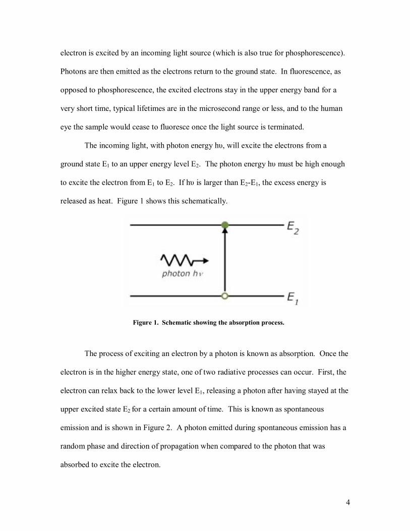
The incoming light, with photon energy hυ, will excite the electrons from a
ground state E1 to an upper energy level E2. The photon energy hυ must be high enough
to excite the electron from E1 to E2. If hυ is larger than E2-E1, the excess energy is
released as heat. Figure 1 shows this schematically.
Figure 1. Schematic showing the absorption process.
The process of exciting an electron by a photon is known as absorption. Once the
electron is in the higher energy state, one of two radiative processes can occur. First, the
electron can relax back to the lower level E1, releasing a photon after having stayed at the
upper excited state E2 for a certain amount of time. This is known as spontaneous
emission and is shown in Figure 2. A photon emitted during spontaneous emission has a
random phase and direction of propagation when compared to the photon that was
absorbed to excite the electron.
5
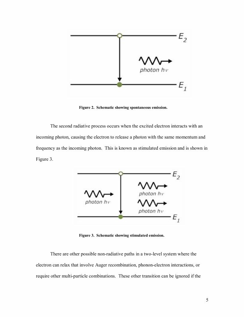
Figure 2. Schematic showing spontaneous emission.
The second radiative process occurs when the excited electron interacts with an
incoming photon, causing the electron to release a photon with the same momentum and
frequency as the incoming photon. This is known as stimulated emission and is shown in
Figure 3.
Figure 3. Schematic showing stimulated emission.
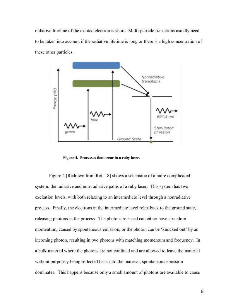
There are other possible non-radiative paths in a two-level system where the
electron can relax that involve Auger recombination, phonon-electron interactions, or
require other multi-particle combinations. These other transition can be ignored if the
6
radiative lifetime of the excited electron is short. Multi-particle transitions usually need
to be taken into account if the radiative lifetime is long or there is a high concentration of
these other particles.
Figure 4. Processes that occur in a ruby laser.
Figure 4 [Redrawn from Ref. 18] shows a schematic of a more complicated
system: the radiative and non-radiative paths of a ruby laser. This system has two
excitation levels, with both relaxing to an intermediate level through a nonradiative
process. Finally, the electrons in the intermediate level relax back to the ground state,
releasing photons in the process. The photons released can either have a random
momentum, caused by spontaneous emission, or the photon can be knocked out by an
incoming photon, resulting in two photons with matching momentum and frequency. In
a bulk material where the photons are not confined and are allowed to leave the material
without purposely being reflected back into the material, spontaneous emission
dominates. This happens because only a small amount of photons are available to cause
7
stimulated emission due to the fact that most photons are emitted in a random direction
and quickly exit the sample. When a structure is used to confine the photons, a buildup
of photons with the same wavelength occurs and the likelihood that an excited electron
relaxes via stimulated emission increases. The point at which the number of photons
emitted by a material is generated equally by spontaneous and stimulated emission is
known as the lasing threshold. A typical structure that is used to enable lasing is an
etalon, where mirrors are used to keep the photons trapped in the material.
2.2 Einstein Coefficients
When an electron is excited, it will have some probability of relaxing on its own
by spontaneous emission. This probability is given by the Einstein coefficient, A. Aij is
defined as the probability per second of a spontaneous jump from level i to level j[17]. If
there are N2 electrons per unit volume in the level 2, then
Rspon=N2A21. Eq. 1
where Rspon is the rate at which electrons will relax from level 2 to level 1 per second.
For a system with no incoming radiation and an initial number of excited electrons, N2o,
the amount of excited electrons after time t will is given by
tAoeNtN 21
22 )( −= . Eq. 2
The time in which the population falls to 1/e of its initial value is called the natural
lifetime of level 2, τ2; where τ2 is equal to 1/A21.
When an excited electron is stimulated by a photon to jump to a lower energy
level, the photon emitted by the electron transition will be in phase with the incoming
photon. The rate at which stimulated emission occurs is given as
Rstim=uvN2B21, Eq. 3
8
where N2 is the number of electrons per unit volume in the upper energy level, B21 is the
probability per second of a stimulated jump from level 2 to level 1, and uv is the spectral
energy density of the incoming photons. B21 is associated with the jump from some
energy level, 2, to a lower energy level, 1 and, hence, is the Einstein coefficient
associated with stimulated emission. .
Electrons make an upward transition by absorbing a photon; this process is known
as absorption. The rate of electrons leaving the lower energy level is
Rabs=uvN1B12. Eq. 4
The spectral energy density, uv, is the same as before and N1 is the number of electrons
per unit volume in the lower energy level. B12 is the final Einstein coefficient, which
governs the rate at which electrons are excited by incoming photons. It is not a
coincidence that equations three and four appear similar; it can be shown that B12 is equal
to B21, and thus stimulated emission is the analogue of absorption. While the rate
equations for stimulated emission and absorption are similar, there is no analogue for
spontaneous emission. An electron cannot spontaneously jump to a higher energy level;
energy for this jump must be provided through a transfer from one or more additional
particles. One important property of equation one, three and four is that the rate of each
process is proportional to the electron population density of the involved energy level.
Finally, it can be shown that there is a relationship between A and B[18]. The
Einstein relations are:
B12=B21 Eq. 5
and
3
3
21
21 8ch
BA υπ= , Eq. 6
9
where c is the speed of light, h is Plancks constant, and ν is the frequency of the photon
emitted as a result of the electrons relaxation from level 2 to level 1. From this equation,
it can be seen that the ratio of A21/B21 increases with increasing frequency (and thus the
energy) of the photon released. Therefore, spontaneous emission is expected to dominant
in systems where there is little confinement of light, uv is small, and the energy of the
emitted photon, λν /hchE photon == , is large.
2.3 Absorption
2.3.1 Direct Bandgap Absorption
To determine the absorption properties of a semiconducting material, the density
of states (DOS), N(E), is important. The DOS represents the number of available states
at an energy level per unit volume[16]. To determine the DOS, the semiconductor is
assumed to have no quantum confinement; the electrons, with effective mass m*, are free
to move in three dimensions. The number of energy states between E and E + dE is then:
( ) dEEmdEEN 23
32 *22
1)(hπ
= , for E ≥ 0. Eq. 7
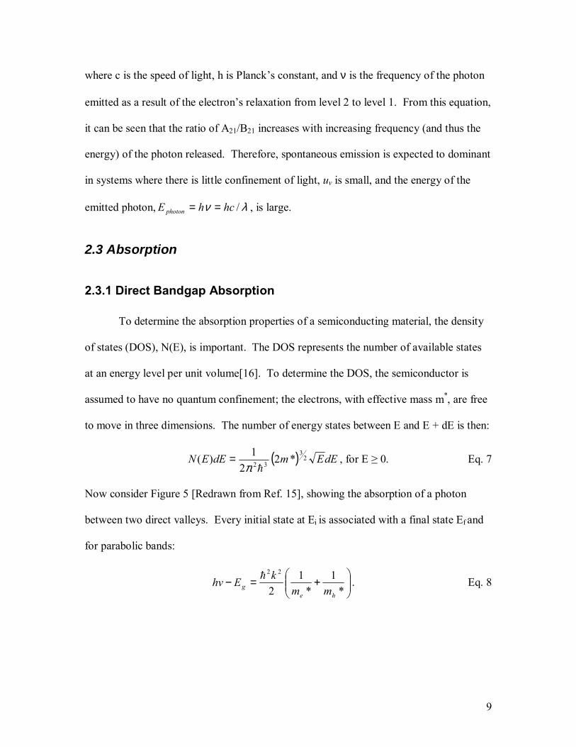
Now consider Figure 5 [Redrawn from Ref. 15], showing the absorption of a photon
between two direct valleys. Every initial state at Ei is associated with a final state Ef and
for parabolic bands:
+=−
*1
*1
2
22
heg mm
kEhv h . Eq. 8
10
Figure 5. E-K diagram showing electron transition.
The effective mass of the electrons and holes are me* and mh
* , respectively. The density
of directly associated states will then be found to be:
gr Ehvmh
EN −= 23
328)( π Eq. 9
where the reduced effective mass is:
****
he
her mm
mmm
+= Eq. 10
where me* is the effective mass of an electron at the bottom of the conduction band and
mh* is the effective mass of a hole (a missing electron) at the top of the valence band.
The absorption coefficient is defined as the relative rate of decrease in light
intensity L(hυ) along its propagation path:
dxhLd
hL)]([
)(1 νν
α = Eq. 11
and is expressed in units of cm-1[16]. The absorption coefficient for a given photon
energy hυ is proportional to the probability for the transition from the initial state to the
11
final state and also the density of available final states. This process must be summed for
all possible transitions between states separated by an energy difference equal to hυ. The
absorption equations shown here were assumed to have all lower states filled and all
upper states empty. This is known as the low light condition where ρ(ν) is very small.
From equation eleven, it can be derived that the absorption coefficient for a direct
bandgap semiconductor is
21
)(*)( gEhAh −= ννα . Eq. 12
A* is constant for any given material and is given by
***
**2
* 2
23
2
e
eh
eh
mnchmm
mmq
A
+
= Eq. 13
where q is the charge on an electron, n is the index of refraction and c is the speed of
light[16].
2.3.2 Band Tailing
Knowing the DOS and carrier concentration is theoretically enough to plot the
absorbance of a semiconductor. But there is a problem that occurs experimentally.
Theory states that when hυ=Eg, N(E)=0, but experimentally this rarely occurs[16].
Perturbations form in the DOS that extend into the conduction and valence bands, thus
the DOS is nonzero extending into the bandgap. These perturbations are caused by
impurities in the crystal. An ionized donor exerts an attractive force on the conduction
electrons and a repulsive force on the valence holes. Acceptors act conversely, and since
the impurities are distributed randomly within the crystal lattice, the local interaction will
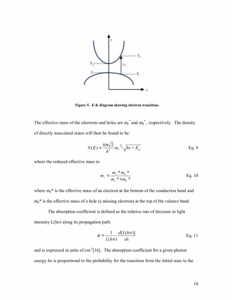
vary over the lattice as impurities cluster inhomogenously. Figure 6 [Redrawn from Ref.
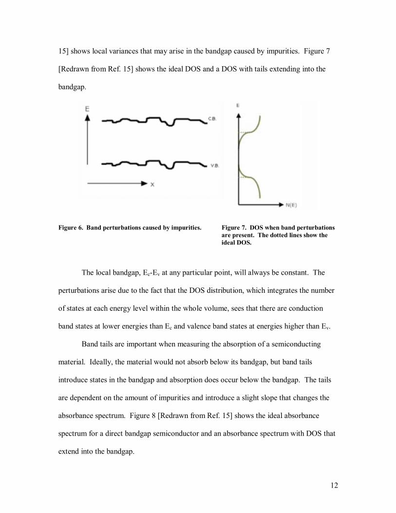
12
15] shows local variances that may arise in the bandgap caused by impurities. Figure 7
[Redrawn from Ref. 15] shows the ideal DOS and a DOS with tails extending into the
bandgap.
Figure 6. Band perturbations caused by impurities. Figure 7. DOS when band perturbations are present. The dotted lines show the ideal DOS.
The local bandgap, Ec-Ev at any particular point, will always be constant. The
perturbations arise due to the fact that the DOS distribution, which integrates the number
of states at each energy level within the whole volume, sees that there are conduction
band states at lower energies than Ec and valence band states at energies higher than Ev.
Band tails are important when measuring the absorption of a semiconducting
material. Ideally, the material would not absorb below its bandgap, but band tails
introduce states in the bandgap and absorption does occur below the bandgap. The tails
are dependent on the amount of impurities and introduce a slight slope that changes the
absorbance spectrum. Figure 8 [Redrawn from Ref. 15] shows the ideal absorbance
spectrum for a direct bandgap semiconductor and an absorbance spectrum with DOS that
extend into the bandgap.
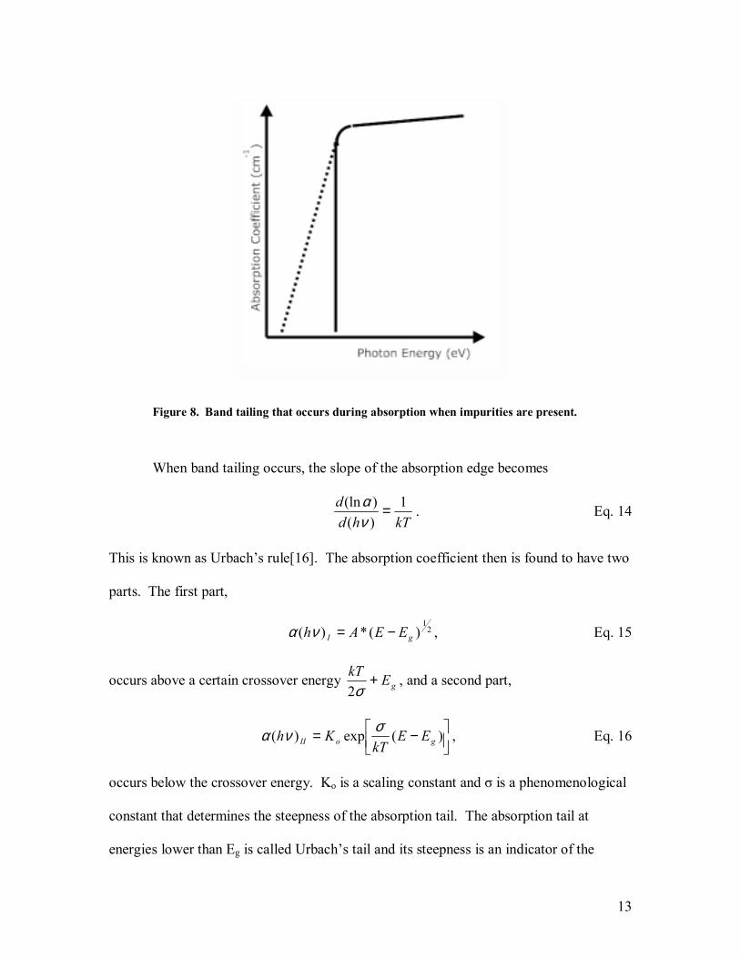
13
Figure 8. Band tailing that occurs during absorption when impurities are present.
When band tailing occurs, the slope of the absorption edge becomes
kThdd 1
)()(ln =
να . Eq. 14
This is known as Urbachs rule[16]. The absorption coefficient then is found to have two
parts. The first part,
21
)(*)( gI EEAh −=να , Eq. 15
occurs above a certain crossover energy gEkT +σ2
, and a second part,
−= )(exp)( goII EEkT
Kh σνα , Eq. 16
occurs below the crossover energy. Ko is a scaling constant and σ is a phenomenological
constant that determines the steepness of the absorption tail. The absorption tail at
energies lower than Eg is called Urbachs tail and its steepness is an indicator of the
14
impurities in the semiconductor, where the smaller the slope of the tail, the higher the
density of impurities present.
2.3.3 Indirect Bandgap Absorption
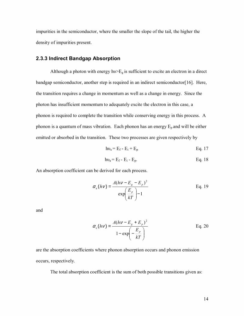
Although a photon with energy hυ>Eg is sufficient to excite an electron in a direct
bandgap semiconductor, another step is required in an indirect semiconductor[16]. Here,
the transition requires a change in momentum as well as a change in energy. Since the
photon has insufficient momentum to adequately excite the electron in this case, a
phonon is required to complete the transition while conserving energy in this process. A
phonon is a quantum of mass vibration. Each phonon has an energy Ep and will be either
emitted or absorbed in the transition. These two processes are given respectively by
hυe = Ef - Ei + Ep Eq. 17
hυa = Ef - Ei - Ep. Eq. 18
An absorption coefficient can be derived for each process.
1exp
)( 2
a
−
−−=)(
kTE
EEhAh
p
pgννα Eq. 19
and
−−
+−=)(
kTEEEhA
hp
pg
exp1
)( 2
e
ννα Eq. 20
are the absorption coefficients where phonon absorption occurs and phonon emission
occurs, respectively.
The total absorption coefficient is the sum of both possible transitions given as:
15
)()()( νανανα hhh ea += .
Here αa(hυ) begins to absorb when hυ = Eg - Ep and αe(hυ) begins to absorb when hυ = Eg
+ Ep. Since the denominator in αe is larger than the denominator in αa, αe is much greater
than αa when hυ > Eg - Ep. However αa is responsible for all of the absorption in the
window +/- Ep around Eg. No absorption takes place when hυ < Eg - Ep. This is shown
schematically in Figure 9 [Redrawn from Ref. 15].
Figure 9. Absorption spectrum of an indirect semiconductor.
2.3.4 Impurity Effects on Indirect Band Transition
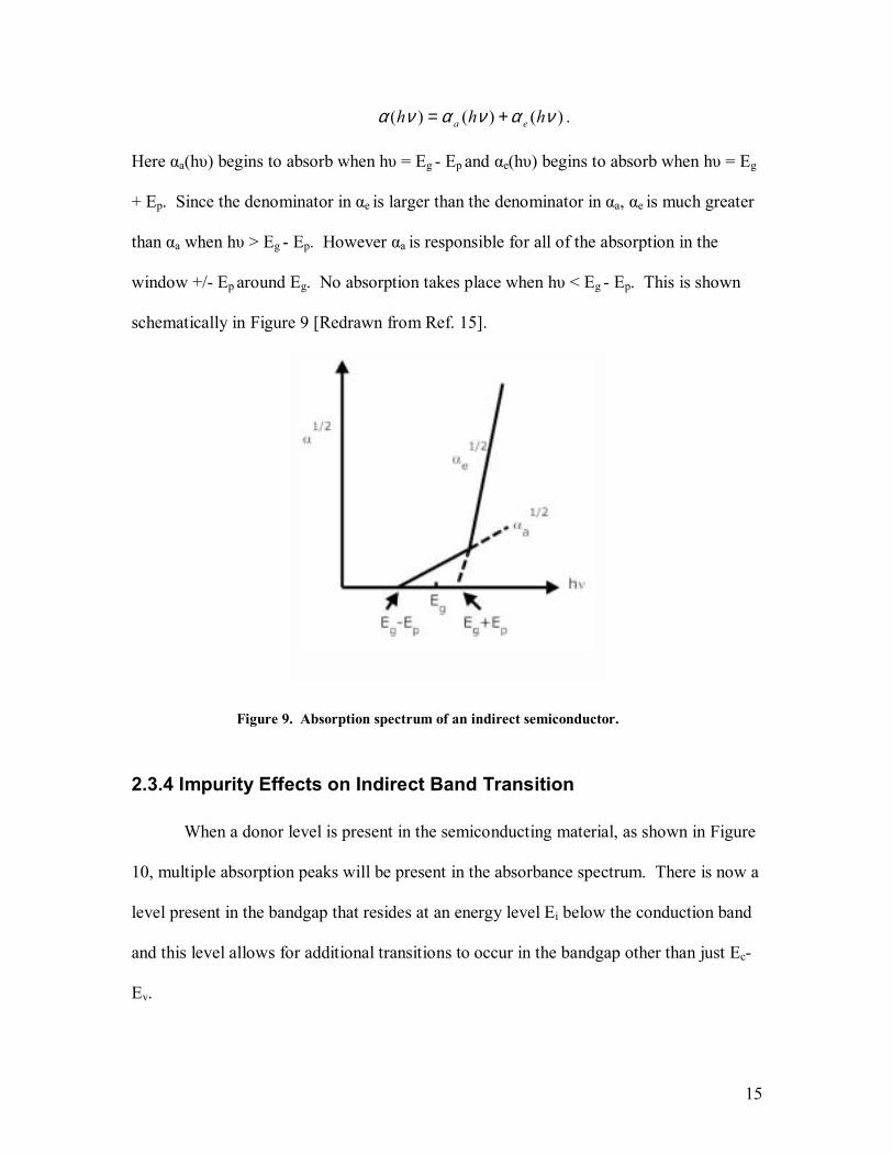
When a donor level is present in the semiconducting material, as shown in Figure
10, multiple absorption peaks will be present in the absorbance spectrum. There is now a
level present in the bandgap that resides at an energy level Ei below the conduction band
and this level allows for additional transitions to occur in the bandgap other than just Ec-
Ev.
16
Figure 10. Bandgap with donor level.
The donor electrons will be excited from Ei to the conduction band when the
incoming photon energy is greater than Ei, emptying the donor band of electrons. Since
Ei is small when the impurity acts as a donor, the ionization energy is low and much
smaller than the bandgap energy. Valence electrons can also be excited to the donor band
when hν > (Ec-Ei) - Ev. This impurity transition energy will be close to the bandgap
transition energy since Ei is small.
An impurity level in the bandgap will be noticeable in the absorbance spectrum if
the quantity of impurities is large. The donor band impurities will occur as a small peak
at an energy amount Ei below the bandgap absorption. This peak will occur close to the
bandgap absorption peak and will appear as a shoulder in the bandgap absorption peak.
The absorption coefficient of the donor level will be proportional to the number of
allowed states in the donor level. Once the incident photon energy becomes greater than
Eg-Ei, electrons will begin to transition from the valence band to the donor level. Since
the DOS of the valence band is greater than the DOS of the donor level, the donor level
will be the limiting factor in how much absorption occurs when hυ = Eg-Ei. The higher
the DOS of the donor level, the higher the absorption coefficient will be. At high donor
17
concentrations and when there are sufficient phonons available to excite the donor
electrons into the conduction band, the absorption coefficient for hν ~ Eg is reduced
because the DOS at the bottom of the conduction band are filled by these donor electrons
so there are no available levels for the valence electrons.
A deep level trap occurs when the donor level is far from the conduction band.
When the donor level is a deep level, the donor peak will be further from the bandgap
absorption peak in an absorbance spectrum and therefore more distinct. However, band
tailing will still convolve the absorption peaks.
These effects are not usually observed when the impurities are acceptors as the
acceptor levels are generally much deeper than that of the donors and, thus, are harder to
populate and depopulate thermally. Also, the DOS of the valence bands are much larger
than the DOS of the conduction band due to the usually larger effective mass of the hole,
mh*. So, it is more difficult to perturb the shape of the valence band in comparison to the
conduction band. In CeO2-γ, there are oxygen vacancies that act as point defects within
the ceria. These point defects form trap states 3 eV above the valence band in the CeO2
bandgap. When the oxygen atoms vacate the crystal, the adjacent cerium ion is reduced
from Ce(IV) to Ce(III). The CeO2, containing Ce(IV) ions, has a bandgap of 4 eV[2].
2.4 Light Scattering
Light scattering is the process where photons, incident on some molecule or
macromolecule, is scattered. The two types of elastic light scattering that occur are
Rayleigh scattering and Mie scattering. The size of the scattering particle is defined as
the ratio of its size and the wavelength of the incident photon written as
18
λπrx 2= . Eq. 21
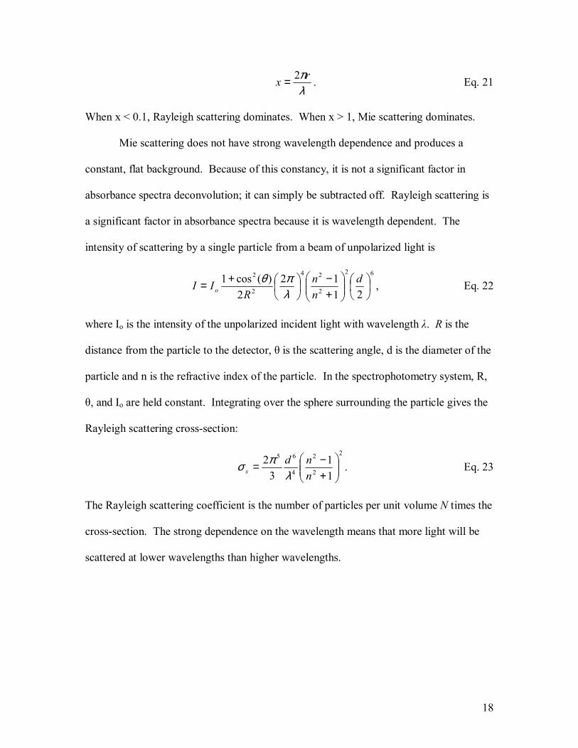
When x < 0.1, Rayleigh scattering dominates. When x > 1, Mie scattering dominates.
Mie scattering does not have strong wavelength dependence and produces a
constant, flat background. Because of this constancy, it is not a significant factor in
absorbance spectra deconvolution; it can simply be subtracted off. Rayleigh scattering is
a significant factor in absorbance spectra because it is wavelength dependent. The
intensity of scattering by a single particle from a beam of unpolarized light is
62
2
24
2
2
2112
2)(cos1
+−
+= d
nn
RII o λ
πθ , Eq. 22
where Io is the intensity of the unpolarized incident light with wavelength λ. R is the
distance from the particle to the detector, θ is the scattering angle, d is the diameter of the
particle and n is the refractive index of the particle. In the spectrophotometry system, R,
θ, and Io are held constant. Integrating over the sphere surrounding the particle gives the
Rayleigh scattering cross-section:
2
2
2
4
65
11
32
+−=
nnd
s λπσ . Eq. 23
The Rayleigh scattering coefficient is the number of particles per unit volume N times the
cross-section. The strong dependence on the wavelength means that more light will be
scattered at lower wavelengths than higher wavelengths.
19
2.5 Cellular Longevity
2.5.1 Free Radical Species in Cells
The free radical theory of aging is currently the most popularly accepted
explanation on how aging occurs at the molecular level due to the fact that it has
significant experimental support[19-21]. The theory states that oxidative stress caused by
free radicals damages cells. Over time the damage accumulates and this buildup of
damage is aging at the molecular level. Oxidative stress has also been identified as a
component in numerous diseases, including atherosclerosis, Arthritis and
neurodegenerative disorders such as Parkinsons and Alzheimers[22,23].
Free radicals are atomic or molecular species that are electron deficient. This
deficiency causes the free radicals to be very reactive and therefore they are likely to take
part in chemical reactions. In biochemistry, the free radicals are often referred to as
reactive oxide species (ROS) due to the fact that the most biologically significant free
radicals are oxygen-centered. However not all ROS are free radicals and not all free
radicals are ROS. Examples of ROS encountered within the cell include lipid
hydroperoxides, superoxide (O2-), the hydroxyl radical (OH), nitric oxide (NO) and
peroxynitrite (ONOO-) among others[10].
ROS are formed regularly inside cells and play an important role in a number of
biological processes required for normal operation. One example is the use of nitric
oxide for intracellular signal transduction. When excess ROS production occurs, the cells
have mechanisms capable of counteracting damage, such as superoxide dismutase,
catalase and endogenous reductants, such as vitamins E and C, carotenes, melatonin and
20
others. When the production of ROS is too much for the innate mechanisms to
counteract, the ROS induce oxidative stress within the cell.
2.5.2 Free Radical Scavengers
The treatment of oxidative stress within the cell is made difficult by the fact that
as an extremely reactive species, free radicals tend not to diffuse far within the cell before
taking part in a potentially damaging reaction. Another difficulty in preventing oxidative
stress is that antioxidants typically have one site for free radical neutralization. This
limits the effectiveness of the antioxidants since areas of oxidative stress can sustain high
amounts of free radicals production.
One alternative to antioxidants that has recently been shown to be effective in
protecting cells from oxidative stress is ceria nanoparticles[8,9]. Adding a dose of ceria
nanoparticles to the intracellular environment of a mixed brain cell culture has been
shown to increase the lifespan by up to six times. In studies where hydrogen peroxide
was used to induce oxidative stress, cell death was decreased by over 60% with a 10nM
dose. Ceria nanoparticles have also been shown to offer significantly greater protection
than other free radical scavengers, such as vitamin E and melatonin, when aggravated by
an ultraviolet light source[10].
The likely mechanism for free radical scavenging in ceria nanoparticles is the
oxidation of the ceria from a Ce(III) state to a Ce(IV) state[8]. As a free radical is
neutralized, a cerium ion is oxidized from the Ce(III) to the Ce(IV) state. Each exposed
Ce(III) ion would act as a free radical neutralizing site and therefore a ten to twenty
nanometer nanoparticle would have many more free radical neutralization sites than the
other free radical scavengers. If reasonably efficient transfer of electrons from the
21
surface Ce(IV) to Ce(III) atoms on the interior of the ceria nanoparticle is permissible,
then the number of neutralization sties can be considered to be even greater. Ceria
nanoparticles have also shown the ability to auto-regenerate over time[24]. They are able
to return to their original concentration of Ce(III) states after being oxidized to Ce(IV),
allowing them to continuously act as free radical scavengers.
Chapter 3 Procedure
3.1 Spectrophotometry
All absorption measurements were made on a Shimadzu UV-3101PC
spectrophotometer. The plots that are generated from the data collected using the
Shimadzu spectrophotometer have wavelength on the x-axis and absorbance on the y-
axis. Absorbance is given by the equation:
( ) ( ) samplereferenceo IIa 1010 loglog −= Eq. 24
Io is the intensity of light passing through the reference cell and I is the intensity of light
passing through the sample cell. By rewriting this equation, the Beer-Lambert law is
obtained:
aoII −= 10 Eq. 25
where
lca α= . Eq. 26
The length of the methacrylate cuvette, l, is 1 cm and absorption at wavelengths above
260 nm is negligible. α is the absorption coefficient, which is a function of wavelength
and is a property of the material used. As can be seen from equations 25 and 26
22
absorbance is higher for a higher concentration, c, of the material through which light
passes.
The absorption experiments in the spectrophotometer were run under two
conditions: colloidal ceria suspended in water and colloidal ceria suspended in an
aqueous solution at an adjusted pH.
For the colloidal ceria suspended in water, each sample was measured at a
concentration of 62.5 µg/mL. These samples were suspended in deionized water with no
additives to adjust the pH and no surfactants. 62.5 µg/mL was chosen as the ceria
concentration for the absorption experiments for two reasons. First, mixing was made
easier. The lowest setting on the micropipettes used is 100 µL, and the samples are
stored at a concentration of 2.5 mg/mL. 100 µL of 2.5 mL/mg ceria and 4 mL of
deionized water (the cuvettes are around 4.5 mL) works out to a ceria concentration of
62.5 mg/µL. The second and more important reason this concentration was used was that
the peak absorbance for the samples was usually around a value of 2 at a wavelength of
300 nm. If the absorbance is too low (<1) the absorption spectrum will be very flat and
will be difficult to resolve the 300 nm and 400 nm absorption peaks. If the absorbance is
too high (>4), only a small amount of photons are incident on the detector, 0.01% of Io
when a=4. In this case, accuracy of the measurement becomes an issue as the optical
signal generated at the detector is not significantly higher than its dark current.
When the hydrogen peroxide, purchased from J.T. Baker, was added to the ceria
solutions, 10 µL of 0.1M was used. Such a small amount of relatively strong hydrogen
peroxide is used to avoid significantly altering the concentration of the sample, which
would affect the absorbance spectrum. All of the absorption measurements for colloidal
23
ceria solutions suspended in pure deionized water, with and without hydrogen peroxide,
were measured in the very slow setting. This allows for maximum resolution and
minimal noise effects.
For the colloidal ceria suspended in a pH adjusted solution, the pH was adjusted
using 0.1 M sodium hydroxide and 0.1 M nitric acid, purchased from Fisher Scientific
and J.T. Baker respectively. Although nitric acid eats away at the plastic beakers that
most of the ceria experiments are run in, its use is necessary for pH adjustment because
the chlorine ions from hydrochloric acid adsorb to the ceria, thus changing the surface
properties of the nanoparticle. The pH of the solutions used ranged from 3.5 to 8.5 with
one unit intervals in between. The molarity of the aqueous, pH adjusted solutions prior to
the introduction of the ceria nanoparticles was on the order of 400 µM.
The pH of the ceria solutions was adjusted by adding 100 µL of 2.5 mg/mL ceria
to an empty cuvette, then injecting 4 mL of the 400 µM aqueous solution into the cuvette,
1 mL at a time. The force of the ejection from the micropipette tip is enough to mix the
two solutions sufficiently. An absorption measurement was then taken, approximately
10-20 seconds after all 4 mL of aqueous solution was injected into the cuvette. Another 4
mL of the 400 µM aqueous pH adjusted solution was used as the sample reference.
For the pH adjusted measurements, the medium measurement speed was used as a
balance between time and accuracy. Three independent absorption spectra were taken for
each sample at each pH value, then averaged together to reduce variation.
All absorption measurements were run from 260 nm to 760 nm. 260 nm is the
shortest wavelength that can be used before the methacrylate cuvettes start to absorb
heavily. Quartz cuvettes could have been used to perform measurements in the 200 nm
24
(the machines lower bound) to 260 nm range, however nothing of interest would have
been found, so methacrylate cuvettes were deemed acceptable and used exclusively. 550
nm was chosen as the upper bound because nothing of interest was noted during our
initial experiments at longer wavelengths. The scattering profile of the sample can be
observed when absorption is run to higher wavelengths,
3.2 Fluorometry
The fluorescence experiments were performed on a dual monochromator Jobin-
Yvon spectrometer. The spectrometer is a machine that passes light through a sample
and measures the fluorescence the sample emits. The light source used was a 250W
tungsten halogen lamp, run at 10A, 20Vdc. The light first passes through a 250 µm slit to
narrow the beam and then sent through an excitation monochromator, with a ruled
diffraction grating (600 lines/mm) blazed at 350 nm. It then passes through another 250
µm slit to narrow the light spectrum incident on the sample. The input to the
fluorescence monochromator had no slit and is set at a 90° angle to the sample,
minimizing scattered light from entering the monochromator. The diffraction grating
used in the fluorescence monochromator was a ruled grating, (600 lines/mm) blazed at
750 nm. A 500 µm slit was placed on the output of the fluorescence monochromator.
The same cuvettes were used in fluorometry as in spectrophotometry. The optical signals
were detected using a photomultiplier tube biased at 950V.
All experiments that were compared relative to each other were performed
immediately following one another in order to prevent anomalies in the data due to
variations in the current running through the tungsten lamp or to a different wavelength
calibration associated with the position of the diffraction grating.
25
All fluorescence experiments were run with the ceria particles suspended in
deionized water. When the pH of the colloidal solution was adjusted away from that of
deionized water (~ pH=5.5), the particles inevitably fell out of solution faster than when
they were suspended in deionized water. Since the fluorometry measurements need a
very accurate concentration of the fluorophore (in this case, the ceria nanoparticles) to
compare the fluorescence intensity of one sample against the fluorescence of another, any
precipitation would skew the results in a random direction. Even at the low molarity used
in the pH adjusted solutions, 400 µM, the particles tended to fall out too quickly to make
accurate comparisons. Therefore, all fluorometry experiments were done with the
particles suspended in deionized water.
The excitation wavelength in the experiments where the fluorescence spectra were
collected was 420 nm and the fluorescence wavelength in the experiments to collect the
excitation spectra was 550 nm. The fluorescence measurements were run with the ceria
solution at 0.3 mg/mL. This concentration was used because it is high enough that a
significant amount of photons will be produced but low enough that the photons can exit
the cuvette with minimal scattering and/or self absorption.
The spectrometer is able to measure fluorescence in two ways. The first is an
excitation scan. During an excitation scan, the fluorescence monochromator is held
constant at 550 nm and the excitation monochromator is scanned across a wavelength
range; the range having a center at 420 nm. The second is a fluorescence scan, which is
the opposite of an excitation scan. Both methods measure the same phenomena, but one
gives information about the excitation spectrum while the other gives information about
the fluorescence spectrum.
26
Once the excitation spectra were measured, the background radiation, caused by
scattered light from the sample, was subtracted from the spectra and the area of the peak
was taken as the amount of fluorescence given off by that sample. The area was
calculated using Origin 7.5 data analysis software made by OriginLab.
3.3 X-Ray Photoelectron Spectroscopy
XPS measurements were performed using a Perkin-Elmer 5400. To prepare the
samples, an aqueous solution of 20% poly-vinyl alcohol (PVA), average mw 13,000-
23,000 and purchased from Aldrich Chemical Company, was prepared. A ceria solution,
suspended in DI water, with a fairly high concentration, ~40 mg/mL, was then added in
equal proportions to the PVA solution to form a 10% PVA solution with a high
concentration of ceria, ~20 mg/mL. A large concentration of ceria is needed due to the
fact that the PVA tends to dominate the XPS spectrum unless the ceria is highly
concentrated. The PVA is used as a dispersant to keep the particles separate while they
dry.
The PVA-ceria solution was then put on a glass microscope slide using a Pasteur
pipette. Enough solution was put on the slide to fully cover it. The slides were dried in
an oven at 70° Celsius for two hours at which point the samples were ready to be loaded
into the Perkin-Elmer 5400 and XPS measurements were carried out.
The areas of interest are the 3d peaks of cerium. There are 10 peaks, with 6 being
associated with Ce(IV) and 4 being associated with Ce(III). All data manipulation is
done with the AugerScan software package, version 3.2, produced by RBD enterprises.
AugerScan is also the software used to control the XPS system. The measurement forms
a continuous spectrum, which must be deconvolved into 10 independent Gaussian peaks.
27
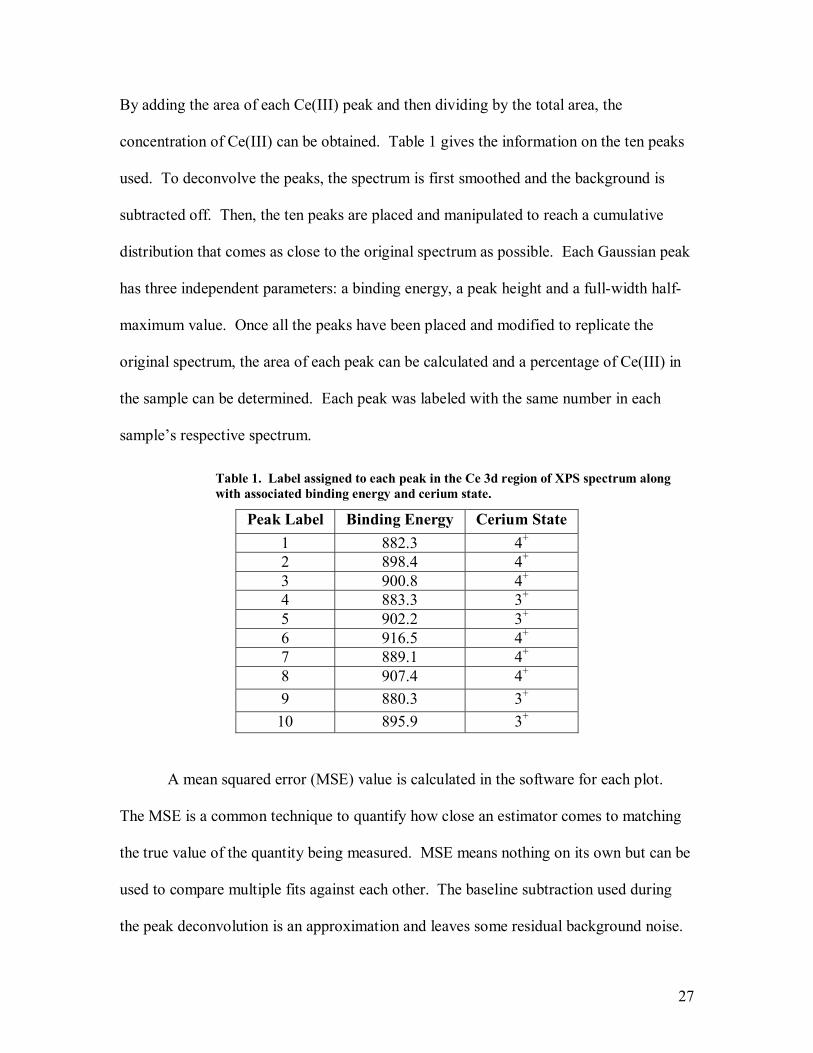
By adding the area of each Ce(III) peak and then dividing by the total area, the
concentration of Ce(III) can be obtained. Table 1 gives the information on the ten peaks
used. To deconvolve the peaks, the spectrum is first smoothed and the background is
subtracted off. Then, the ten peaks are placed and manipulated to reach a cumulative
distribution that comes as close to the original spectrum as possible. Each Gaussian peak
has three independent parameters: a binding energy, a peak height and a full-width half-
maximum value. Once all the peaks have been placed and modified to replicate the
original spectrum, the area of each peak can be calculated and a percentage of Ce(III) in
the sample can be determined. Each peak was labeled with the same number in each
samples respective spectrum.
Table 1. Label assigned to each peak in the Ce 3d region of XPS spectrum along with associated binding energy and cerium state.
Peak Label Binding Energy Cerium State 1 882.3 4+ 2 898.4 4+ 3 900.8 4+ 4 883.3 3+ 5 902.2 3+ 6 916.5 4+ 7 889.1 4+ 8 907.4 4+ 9 880.3 3+
10 895.9 3+
A mean squared error (MSE) value is calculated in the software for each plot.
The MSE is a common technique to quantify how close an estimator comes to matching
the true value of the quantity being measured. MSE means nothing on its own but can be
used to compare multiple fits against each other. The baseline subtraction used during
the peak deconvolution is an approximation and leaves some residual background noise.
28
This noise tends to show up in the spectra between peaks 6 and 8 and between peaks 7
and 10. These remnants are ignored when the peaks are placed, but tend to inflate the
MSE value. It was thus attempted to get the MSE values as low as possible, and all
clustered closely, while ignoring the background remnants.
3.4 Dynamic Light Scattering
DLS was used to obtain the intensity-weighted particle hydrodynamic diameter in
aqueous solution. A Malvern Zetasizer NanoZS compact scattering spectrometer
(Malvern Instruments Ltd, Malvern, UK) at a wavelength of 633 nm with a 4.0 mW He-
Ne laser was used at a scattering angle of 173°.
3.5 Transmission Electron Microscopy
TEM was performed on each sample in order to gain visual information about the
particles. The TEM used was a Philips EM420T. Samples were prepared by drying a
drop of dilute colloidal ceria on a carbon-coated copper TEM grid (400 mesh).
3.6 Brunauer-Emmitt-Teller
Surface areas of the cerium oxide nanoparticles were measured by performing
BET 6-point scans using a Micromeritics ASAP 2000 nitrogen adsorption instrument.
The BET measurement can be used to calculate the diameter of the particles. The
specific surface area of a particle is given by
SSA = 6/ρD, Eq. 27
where ρ is the density of the material, and D is the diameter of the particle. The density
of ceria is 7 g/cm3. The particles were assumed to be spherical and nonporous. Since it
29
can be seen from the TEM images that the particles are not exactly spherical, the
diameter as determined from BET is treated as an approximation.
3.7 X-Ray Diffraction
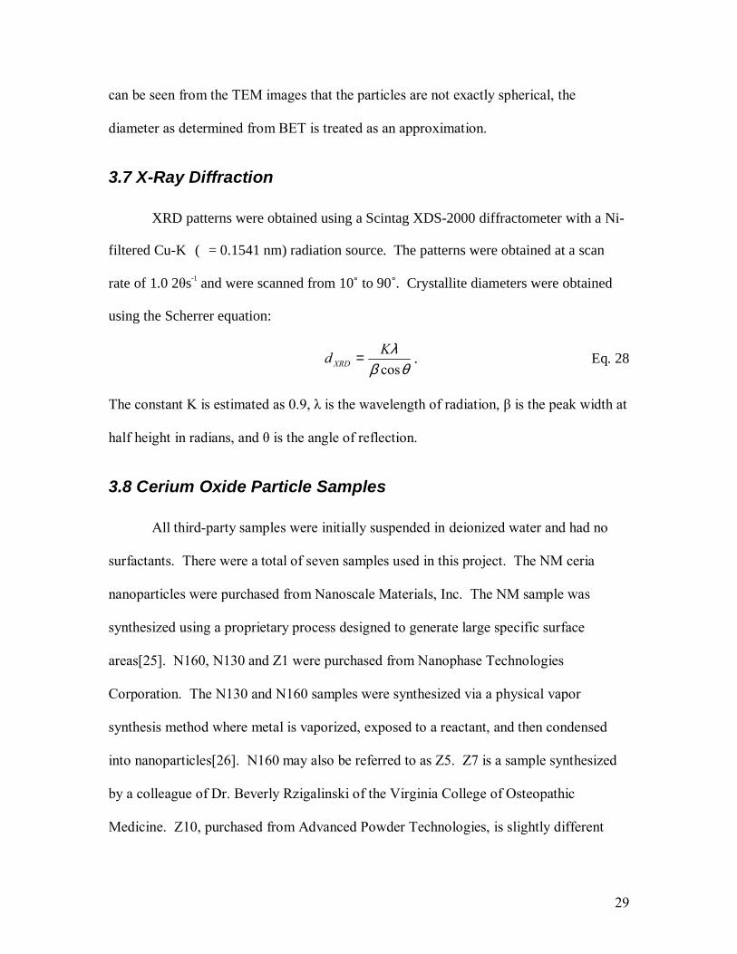
XRD patterns were obtained using a Scintag XDS-2000 diffractometer with a Ni-
filtered Cu-K ( = 0.1541 nm) radiation source. The patterns were obtained at a scan
rate of 1.0 2θs-1 and were scanned from 10˚ to 90˚. Crystallite diameters were obtained
using the Scherrer equation:
θβλ
cosKd XRD = . Eq. 28
The constant K is estimated as 0.9, λ is the wavelength of radiation, β is the peak width at
half height in radians, and θ is the angle of reflection.
3.8 Cerium Oxide Particle Samples
All third-party samples were initially suspended in deionized water and had no
surfactants. There were a total of seven samples used in this project. The NM ceria
nanoparticles were purchased from Nanoscale Materials, Inc. The NM sample was
synthesized using a proprietary process designed to generate large specific surface
areas[25]. N160, N130 and Z1 were purchased from Nanophase Technologies
Corporation. The N130 and N160 samples were synthesized via a physical vapor
synthesis method where metal is vaporized, exposed to a reactant, and then condensed
into nanoparticles[26]. N160 may also be referred to as Z5. Z7 is a sample synthesized
by a colleague of Dr. Beverly Rzigalinski of the Virginia College of Osteopathic
Medicine. Z10, purchased from Advanced Powder Technologies, is slightly different
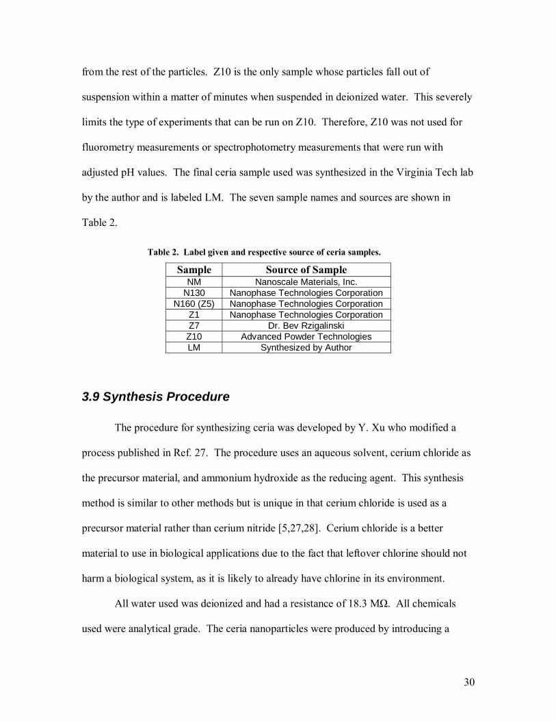
30
from the rest of the particles. Z10 is the only sample whose particles fall out of
suspension within a matter of minutes when suspended in deionized water. This severely
limits the type of experiments that can be run on Z10. Therefore, Z10 was not used for
fluorometry measurements or spectrophotometry measurements that were run with
adjusted pH values. The final ceria sample used was synthesized in the Virginia Tech lab
by the author and is labeled LM. The seven sample names and sources are shown in
Table 2.
Table 2. Label given and respective source of ceria samples.
Sample Source of Sample NM Nanoscale Materials, Inc.
N130 Nanophase Technologies Corporation N160 (Z5) Nanophase Technologies Corporation
Z1 Nanophase Technologies Corporation Z7 Dr. Bev Rzigalinski
Z10 Advanced Powder Technologies LM Synthesized by Author
3.9 Synthesis Procedure
The procedure for synthesizing ceria was developed by Y. Xu who modified a
process published in Ref. 27. The procedure uses an aqueous solvent, cerium chloride as
the precursor material, and ammonium hydroxide as the reducing agent. This synthesis
method is similar to other methods but is unique in that cerium chloride is used as a
precursor material rather than cerium nitride [5,27,28]. Cerium chloride is a better
material to use in biological applications due to the fact that leftover chlorine should not
harm a biological system, as it is likely to already have chlorine in its environment.
All water used was deionized and had a resistance of 18.3 MΩ. All chemicals
used were analytical grade. The ceria nanoparticles were produced by introducing a
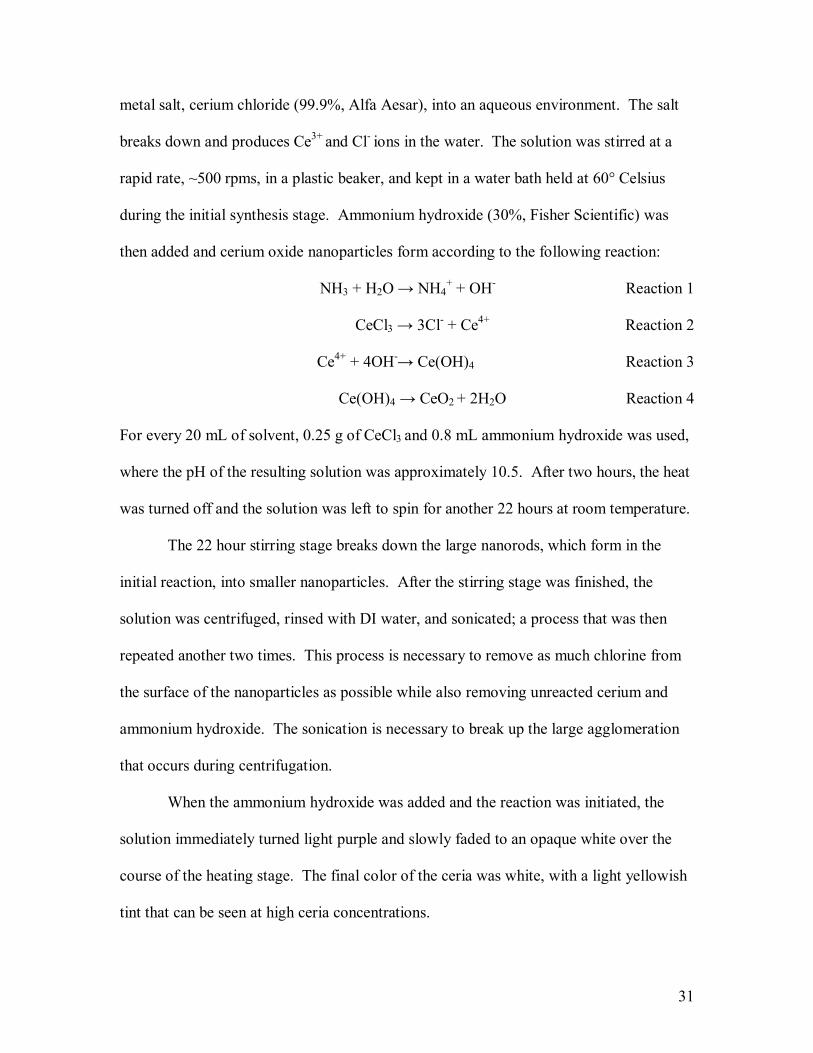
31
metal salt, cerium chloride (99.9%, Alfa Aesar), into an aqueous environment. The salt
breaks down and produces Ce3+ and Cl- ions in the water. The solution was stirred at a
rapid rate, ~500 rpms, in a plastic beaker, and kept in a water bath held at 60° Celsius
during the initial synthesis stage. Ammonium hydroxide (30%, Fisher Scientific) was
then added and cerium oxide nanoparticles form according to the following reaction:
NH3 + H2O → NH4+ + OH- Reaction 1
CeCl3 → 3Cl- + Ce4+ Reaction 2
Ce4+ + 4OH-→ Ce(OH)4 Reaction 3
Ce(OH)4 → CeO2 + 2H2O Reaction 4
For every 20 mL of solvent, 0.25 g of CeCl3 and 0.8 mL ammonium hydroxide was used,
where the pH of the resulting solution was approximately 10.5. After two hours, the heat
was turned off and the solution was left to spin for another 22 hours at room temperature.
The 22 hour stirring stage breaks down the large nanorods, which form in the
initial reaction, into smaller nanoparticles. After the stirring stage was finished, the
solution was centrifuged, rinsed with DI water, and sonicated; a process that was then
repeated another two times. This process is necessary to remove as much chlorine from
the surface of the nanoparticles as possible while also removing unreacted cerium and
ammonium hydroxide. The sonication is necessary to break up the large agglomeration
that occurs during centrifugation.
When the ammonium hydroxide was added and the reaction was initiated, the
solution immediately turned light purple and slowly faded to an opaque white over the
course of the heating stage. The final color of the ceria was white, with a light yellowish
tint that can be seen at high ceria concentrations.
32
Lab-made ceria solutions that were centrifuged once were the particles used in the
experiments presented in this report, and are labeled LM. LM particles are only
centrifuged once because after the second and third centrifuge steps, a significant amount
of ceria particles are washed off and discarded. Thus if an exact concentration is needed,
centrifugation can only be run once. LM has a higher salt concentration than a sample
that has been fully washed, but it has a known ceria concentration. Assuming full
reactivity of the reactants, the concentration after the first wash can be calculated based
on the amount of cerium chloride used. Having a known concentration is critical for the
spectroscopy techniques used. An assumption was made that the differences between
ceria washed three times versus ceria washed once were small and unlikely to affect
experimentation results. No polymers were used in the synthesis process, either to coat
the particles and prevent agglomeration[29], or to selectively grow on specific crystal
planes[30]. No dopants were used to alter the reactivity of the ceria[31,32].
Chapter 4 Results and discussion
4.1 Introduction
In its most common form, ceria is stable in the nonstoichiometric form CeO2-γ,
where 5.0 ≤≤ γ . In stoichiometric CeO2, all of the cerium is in the Ce(IV) state. In
nonstoichiometric cerium dioxide, another form of cerium oxide, Ce2O3, is present, where
the cerium is in the Ce(III) state[33]. The reduction of the CeO2 to CeO2-γ is caused by
oxygen atoms vacating the crystal lattice, causing the cerium ions adjacent to the vacancy
sites to reduce from Ce(IV) to Ce(III) [34]. The oxygen vacancies that form, leaving
33
oxygen depleted Ce(III) ion behind, are believed to be the cause for the high reactivity in
ceria[35].
Cerium oxide has a cubic fluorite structure, both in bulk and nanoparticle
form[36]. The low index exposed crystal planes have been shown to have differing
reactivity[37]. The 111 surface plane is the most stable, followed by the 110 and
100 planes. The formation of an oxygen vacancy occurs more easily for the 110
surfaces than in the 111 surfaces. The vacancies tend to form in the surface layer for
110 whereas for the 111 surface they tend to form in the subsurface layer[38].
Quantum confinement is not considered when analyzing ceria nanoparticles. If
quantum confinement of the electrons and holes were present, then a blue-shift would
occur in the absorption curves for smaller particles. In published studies, smaller
particles have shown a red-shifted bandgap[2]. The reason ceria nanoparticles have an
opposite effect to that observed in other semiconducting nanoparticles is not because of a
quantum mechanical phenomenon, but rather that, as the particles get smaller, they have a
higher ratio of Ce(III) to Ce(IV)[39-41]. This increase in Ce(III) ions within the crystal
lattice causes a red shift in the absorbance of the material; attributable to the defect states
associated with the Ce(III) ions and oxygen vacancies. The defect states reside 3eV
above the CeO2 valence band. The CeO2, containing Ce(IV) ions, has a bandgap of 4eV.
As the concentration of Ce(III) ions increases, the concentration of Ce(IV) ions decreases
and more absorption will occur at 3eV and less at 4eV, causing a redshift in the
absorption spectrum.
34
4.2 Particle Size
4.2.1 Sample Size Comparison
Table 3 shows the agglomeration size, as determined by DLS, the individual
particle size, as determined by TEM, XRD and BET, and the specific surface area of each
sample, as determined by BET. The TEM particle size is given as a range. BET and
XRD were not performed on all samples.
There is two size ranges as determined by the TEM images given for the samples.
This is due to the fact that the Z7 sample and the Nanophase samples possess a very wide
size distribution. In reality, there is no discreet break between the large and small
particles in these samples. The large and small particles are separated here because
important information about the exposed surface planes can be determined by examining
the large particles while the small particles are too small to view anything of value.
Table 3. The particle size as determined from TEM, diameter measured by DLS, crystallite size determined from XRD, specific surface area measured from BET and diameter calculated from specific surface area.
Sample TEM-Small
Particle Size
Range(nm)
TEM-Large
Particle Size Range
(nm)
DLS- Diameter
(nm)
XRD- CrystalliteSize (nm)
BET- Specific Surface
Area (m2/g)
BET- Diameter
(nm)
NM 5-7 None 245 4.2 86.0 10.0 N130 4-6 15-100 130 N/A 88.6 9.7 N160 3-10 10-150 160 37.9 24.6 34.8
Z1 3-10 10-80 160 N/A N/A N/A Z7 3-10 10-150 152 N/A N/A N/A Z10 4-6 None 184 N/A N/A N/A LM 7-9 None 114 N/A 55.9 15.3
35
4.2.2 NM
The DLS size of the NM sample, 245 nm, indicates that there is a great deal of
agglomeration, which was confirmed from the TEM images shown in Figure 11. There
are no visible single particles in the TEM images, all the particles have agglomerated.
There appears to be a narrow size distribution with the NM particles. The individual
particle range as determined from TEM, 5-7 nm, matches well with the crystallite size,
4.2 nm, and the particle size as determined by BET, 10 nm.
Figure 11. TEM image of NM.
36
4.2.3 N130
There were two types of particles present in the TEM images of the N130 sample,
shown in Figure 12. There were small particles with an average diameter of 5 nm as
determined from the TEM images. These form smaller agglomerates than the NM
particles. Particles with eight faces forming an octahedron shape are also present. These
octahedra are larger particles, ranging from 15 to 100 nm in diameter, and show little to
no agglomeration. The octahedra appear to have the 111 crystal facet exposed on all
eight faces. The primary particles are too small to observe which crystal facets are
exposed.
Figure 12. TEM image of N130.
37
4.2.4 N160
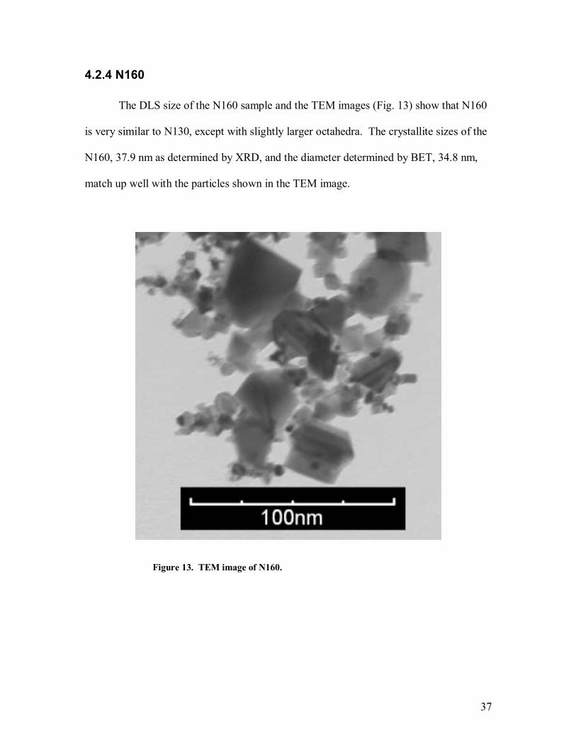
The DLS size of the N160 sample and the TEM images (Fig. 13) show that N160
is very similar to N130, except with slightly larger octahedra. The crystallite sizes of the
N160, 37.9 nm as determined by XRD, and the diameter determined by BET, 34.8 nm,
match up well with the particles shown in the TEM image.
Figure 13. TEM image of N160.
38
4.2.5 Z1
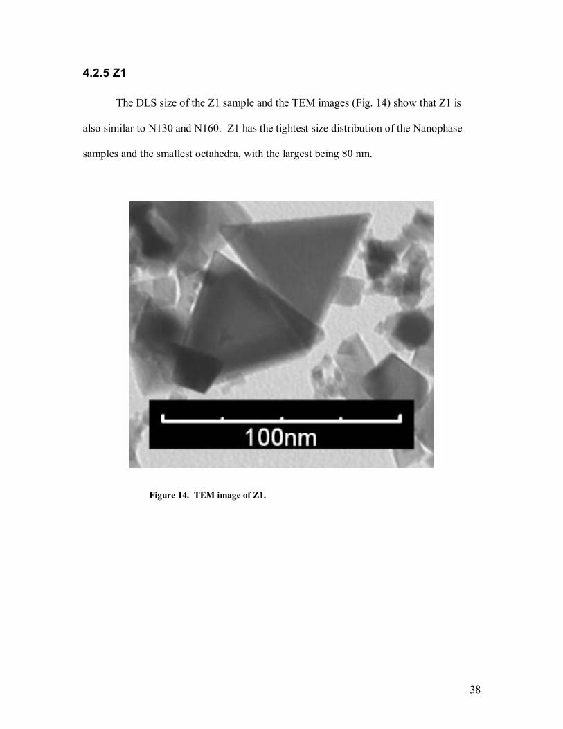
The DLS size of the Z1 sample and the TEM images (Fig. 14) show that Z1 is
also similar to N130 and N160. Z1 has the tightest size distribution of the Nanophase
samples and the smallest octahedra, with the largest being 80 nm.
Figure 14. TEM image of Z1.
39
4.2.6 Z7
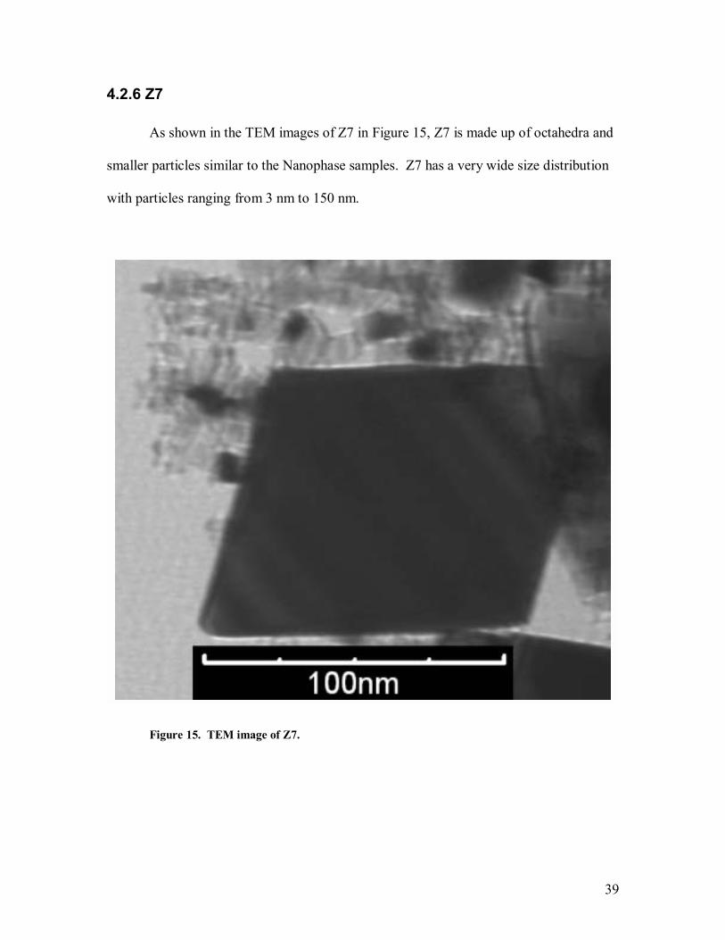
As shown in the TEM images of Z7 in Figure 15, Z7 is made up of octahedra and
smaller particles similar to the Nanophase samples. Z7 has a very wide size distribution
with particles ranging from 3 nm to 150 nm.
Figure 15. TEM image of Z7.
40
4.2.7 Z10
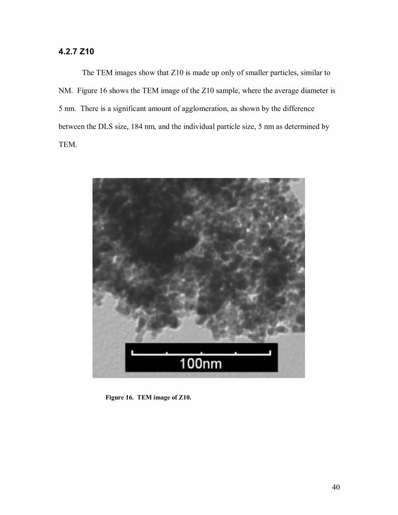
The TEM images show that Z10 is made up only of smaller particles, similar to
NM. Figure 16 shows the TEM image of the Z10 sample, where the average diameter is
5 nm. There is a significant amount of agglomeration, as shown by the difference
between the DLS size, 184 nm, and the individual particle size, 5 nm as determined by
TEM.
Figure 16. TEM image of Z10.
41
4.2.8 LM
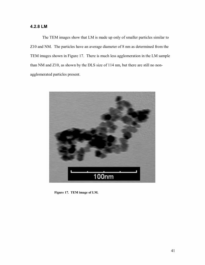
The TEM images show that LM is made up only of smaller particles similar to
Z10 and NM. The particles have an average diameter of 8 nm as determined from the
TEM images shown in Figure 17. There is much less agglomeration in the LM sample
than NM and Z10, as shown by the DLS size of 114 nm, but there are still no non-
agglomerated particles present.
Figure 17. TEM image of LM.
42
4.3 Characterization
4.3.1 Spectrophotometry
The spectrophotometry results can give important insight into the band properties
of cerium oxide. In a defect-free semiconducting crystal, the absorbance will be nearly
zero at low energy until photon energy approaches the bandgap energy of the crystal [16],
at which point the absorption should increase rapidly. When a small concentration of a
second material that possesses lower band gap energy is present in the crystal or defects
are present that modify the DOS, the slope of the absorption edge will lessen. In
traditional optoelectronical studies, these ions are considered defects and are
undesirable[16]. However in cerium oxide, the Ce(III) ions that arise near oxygen
vacancies and near grain boundaries are desirable from a reactivity standpoint. Many
studies have been done to synthesize particles that have a higher ratio of Ce(III)/Ce(IV)
[5,41,42].
The band gap of CeO2 is roughly 4eV[2]. This is an indirect gap of the O2P to the
Ce4f molecular transition. Ce(III) ions present in the crystal lattice create a trap state 3
eV above the CeO2 valence band and correspond to the Ce5d - Ce4f transition. A photon
with 3 eV of energy will possess a wavelength of approximately 413 nm and a photon
with 4 eV of energy will possess a wavelength of approximately 310 nm. To determine
whether scattering would be an issue, the DLS size was put into equation 21. In the
visible wavelength range and for the size of aggregated particles this study deals with,
Rayleigh scattering should not be a factor and Mie scattering should dominate. Since
Mie scattering is not wavelength dependent, it is easily removed from the spectra through
a baseline subtraction. Figure 18 shows the spectra of all seven samples, each at 61
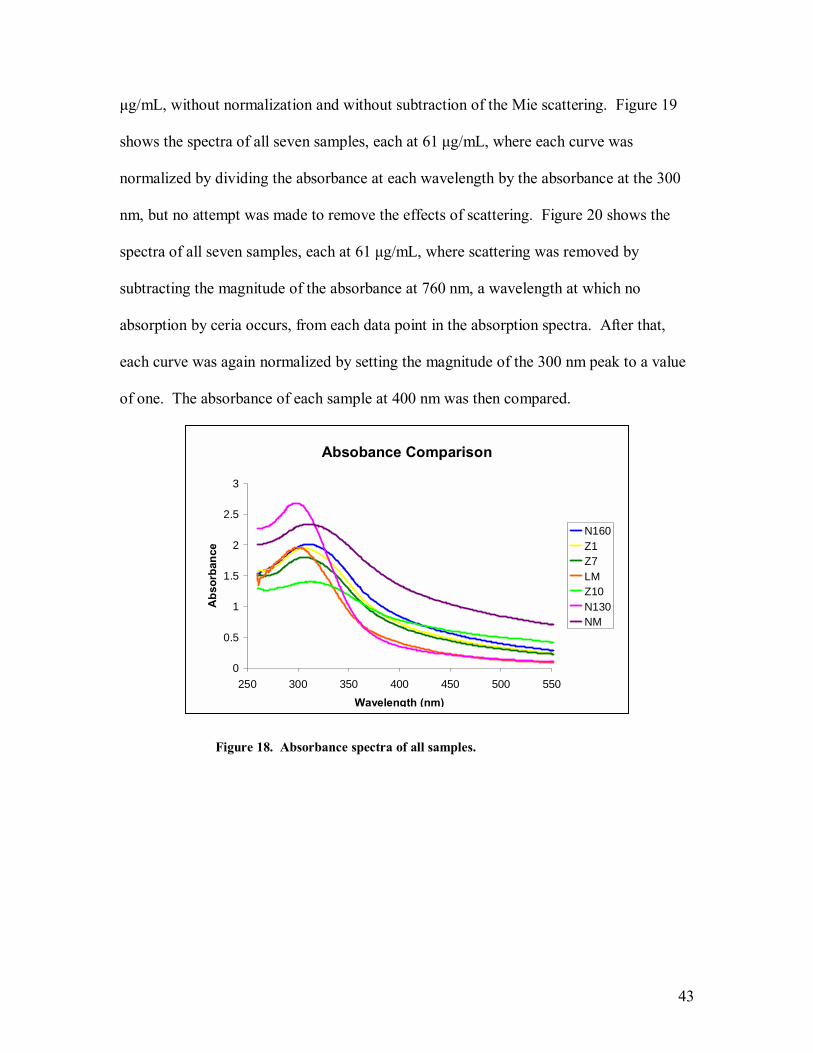
43
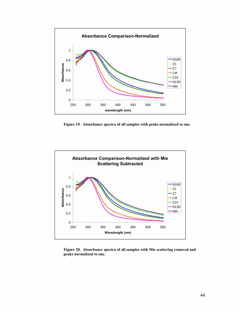
µg/mL, without normalization and without subtraction of the Mie scattering. Figure 19
shows the spectra of all seven samples, each at 61 µg/mL, where each curve was
normalized by dividing the absorbance at each wavelength by the absorbance at the 300
nm, but no attempt was made to remove the effects of scattering. Figure 20 shows the
spectra of all seven samples, each at 61 µg/mL, where scattering was removed by
subtracting the magnitude of the absorbance at 760 nm, a wavelength at which no
absorption by ceria occurs, from each data point in the absorption spectra. After that,
each curve was again normalized by setting the magnitude of the 300 nm peak to a value
of one. The absorbance of each sample at 400 nm was then compared.
Figure 18. Absorbance spectra of all samples.
Absobance Comparison
0
0.5
1
1.5
2
2.5
3
250 300 350 400 450 500 550Wavelength (nm)
Abs
orba
nce
N160Z1Z7LMZ10N130NM
44
Figure 19. Absorbance spectra of all samples with peaks normalized to one.
Figure 20. Absorbance spectra of all samples with Mie scattering removed and peaks normalized to one.
Absorbance Comparison-Normalized with Mie Scattering Subtracted
0
0.2
0.4
0.6
0.8
1
250 300 350 400 450 500 550Wavelength (nm)
Abs
orba
nce
N160Z1Z7LMZ10N130NM
Absorbance Comparison-Normalized
0
0.2
0.4
0.6
0.8
1
250 300 350 400 450 500 550wavelength (nm)
Abs
orba
nce
N160Z1Z7LMZ10N130NM
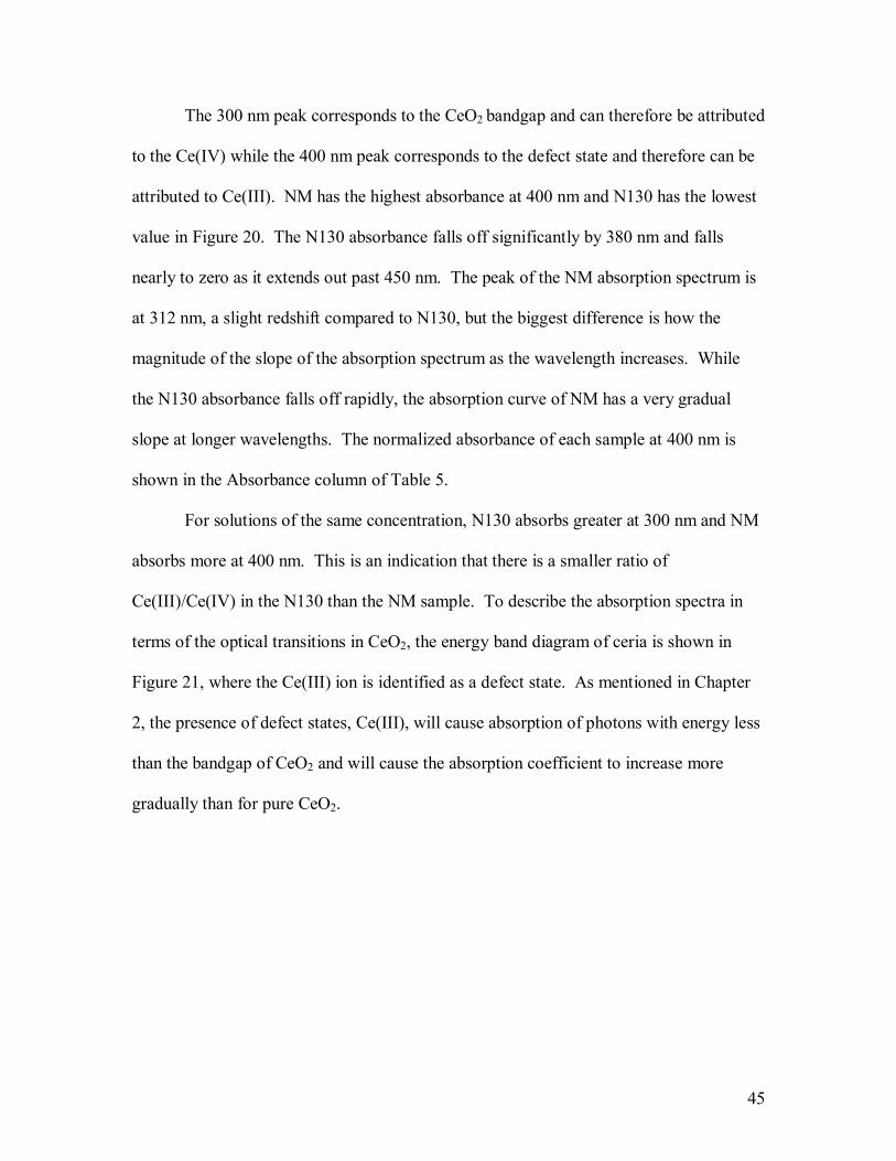
45
The 300 nm peak corresponds to the CeO2 bandgap and can therefore be attributed
to the Ce(IV) while the 400 nm peak corresponds to the defect state and therefore can be
attributed to Ce(III). NM has the highest absorbance at 400 nm and N130 has the lowest
value in Figure 20. The N130 absorbance falls off significantly by 380 nm and falls
nearly to zero as it extends out past 450 nm. The peak of the NM absorption spectrum is
at 312 nm, a slight redshift compared to N130, but the biggest difference is how the
magnitude of the slope of the absorption spectrum as the wavelength increases. While
the N130 absorbance falls off rapidly, the absorption curve of NM has a very gradual
slope at longer wavelengths. The normalized absorbance of each sample at 400 nm is
shown in the Absorbance column of Table 5.
For solutions of the same concentration, N130 absorbs greater at 300 nm and NM
absorbs more at 400 nm. This is an indication that there is a smaller ratio of
Ce(III)/Ce(IV) in the N130 than the NM sample. To describe the absorption spectra in
terms of the optical transitions in CeO2, the energy band diagram of ceria is shown in
Figure 21, where the Ce(III) ion is identified as a defect state. As mentioned in Chapter
2, the presence of defect states, Ce(III), will cause absorption of photons with energy less
than the bandgap of CeO2 and will cause the absorption coefficient to increase more
gradually than for pure CeO2.
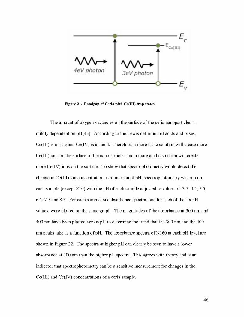
46
Figure 21. Bandgap of Ceria with Ce(III) trap states.
The amount of oxygen vacancies on the surface of the ceria nanoparticles is
mildly dependent on pH[43]. According to the Lewis definition of acids and bases,
Ce(III) is a base and Ce(IV) is an acid. Therefore, a more basic solution will create more
Ce(III) ions on the surface of the nanoparticles and a more acidic solution will create
more Ce(IV) ions on the surface. To show that spectrophotometry would detect the
change in Ce(III) ion concentration as a function of pH, spectrophotometry was run on
each sample (except Z10) with the pH of each sample adjusted to values of: 3.5, 4.5, 5.5,
6.5, 7.5 and 8.5. For each sample, six absorbance spectra, one for each of the six pH
values, were plotted on the same graph. The magnitudes of the absorbance at 300 nm and
400 nm have been plotted versus pH to determine the trend that the 300 nm and the 400
nm peaks take as a function of pH. The absorbance spectra of N160 at each pH level are
shown in Figure 22. The spectra at higher pH can clearly be seen to have a lower
absorbance at 300 nm than the higher pH spectra. This agrees with theory and is an
indicator that spectrophotometry can be a sensitive measurement for changes in the
Ce(III) and Ce(IV) concentrations of a ceria sample.
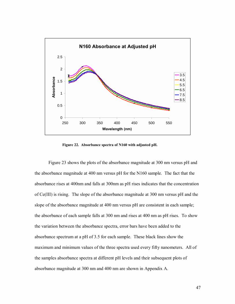
47
Figure 22. Absorbance spectra of N160 with adjusted pH.
Figure 23 shows the plots of the absorbance magnitude at 300 nm versus pH and
the absorbance magnitude at 400 nm versus pH for the N160 sample. The fact that the
absorbance rises at 400nm and falls at 300nm as pH rises indicates that the concentration
of Ce(III) is rising. The slope of the absorbance magnitude at 300 nm versus pH and the
slope of the absorbance magnitude at 400 nm versus pH are consistent in each sample;
the absorbance of each sample falls at 300 nm and rises at 400 nm as pH rises. To show
the variation between the absorbance spectra, error bars have been added to the
absorbance spectrum at a pH of 3.5 for each sample. These black lines show the
maximum and minimum values of the three spectra used every fifty nanometers. All of
the samples absorbance spectra at different pH levels and their subsequent plots of
absorbance magnitude at 300 nm and 400 nm are shown in Appendix A.
N160 Absorbance at Adjusted pH
0
0.5
1
1.5
2
2.5
250 300 350 400 450 500 550Wavelength (nm)
Abs
orba
nce 3.5
4.55.56.57.58.5
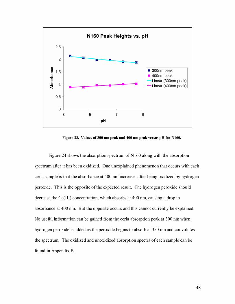
48
Figure 23. Values of 300 nm peak and 400 nm peak versus pH for N160.
Figure 24 shows the absorption spectrum of N160 along with the absorption
spectrum after it has been oxidized. One unexplained phenomenon that occurs with each
ceria sample is that the absorbance at 400 nm increases after being oxidized by hydrogen
peroxide. This is the opposite of the expected result. The hydrogen peroxide should
decrease the Ce(III) concentration, which absorbs at 400 nm, causing a drop in
absorbance at 400 nm. But the opposite occurs and this cannot currently be explained.
No useful information can be gained from the ceria absorption peak at 300 nm when
hydrogen peroxide is added as the peroxide begins to absorb at 350 nm and convolutes
the spectrum. The oxidized and unoxidized absorption spectra of each sample can be
found in Appendix B.
N160 Peak Heights vs. pH
0
0.5
1
1.5
2
2.5
3 5 7 9pH
Abs
orba
nce
300nm peak400nm peakLinear (300nm peak)Linear (400nm peak)
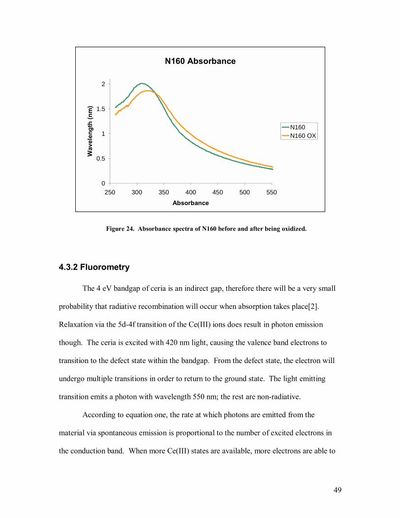
49
Figure 24. Absorbance spectra of N160 before and after being oxidized.
4.3.2 Fluorometry
The 4 eV bandgap of ceria is an indirect gap, therefore there will be a very small
probability that radiative recombination will occur when absorption takes place[2].
Relaxation via the 5d-4f transition of the Ce(III) ions does result in photon emission
though. The ceria is excited with 420 nm light, causing the valence band electrons to
transition to the defect state within the bandgap. From the defect state, the electron will
undergo multiple transitions in order to return to the ground state. The light emitting
transition emits a photon with wavelength 550 nm; the rest are non-radiative.
According to equation one, the rate at which photons are emitted from the
material via spontaneous emission is proportional to the number of excited electrons in
the conduction band. When more Ce(III) states are available, more electrons are able to
N160 Absorbance
0
0.5
1
1.5
2
250 300 350 400 450 500 550
Absorbance
Wav
elen
gth
(nm
)
N160N160 OX
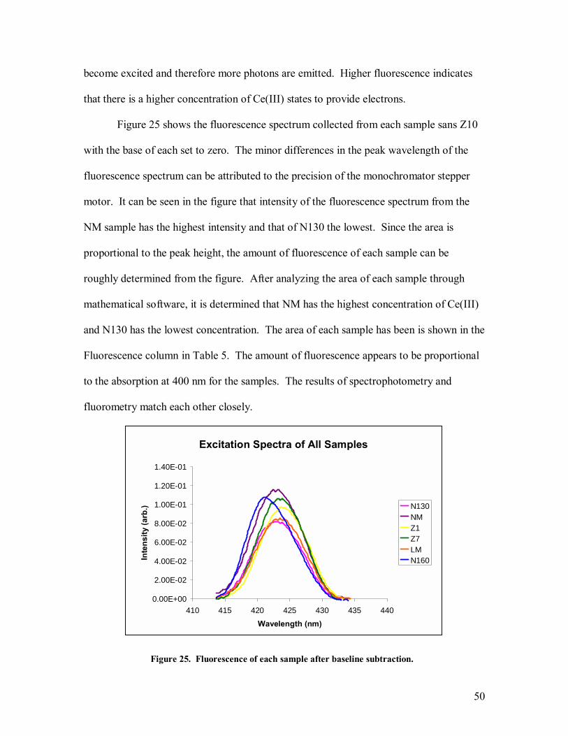
50
become excited and therefore more photons are emitted. Higher fluorescence indicates
that there is a higher concentration of Ce(III) states to provide electrons.
Figure 25 shows the fluorescence spectrum collected from each sample sans Z10
with the base of each set to zero. The minor differences in the peak wavelength of the
fluorescence spectrum can be attributed to the precision of the monochromator stepper
motor. It can be seen in the figure that intensity of the fluorescence spectrum from the
NM sample has the highest intensity and that of N130 the lowest. Since the area is
proportional to the peak height, the amount of fluorescence of each sample can be
roughly determined from the figure. After analyzing the area of each sample through
mathematical software, it is determined that NM has the highest concentration of Ce(III)
and N130 has the lowest concentration. The area of each sample has been is shown in the
Fluorescence column in Table 5. The amount of fluorescence appears to be proportional
to the absorption at 400 nm for the samples. The results of spectrophotometry and
fluorometry match each other closely.
Figure 25. Fluorescence of each sample after baseline subtraction.
Excitation Spectra of All Samples
0.00E+00
2.00E-02
4.00E-02
6.00E-02
8.00E-02
1.00E-01
1.20E-01
1.40E-01
410 415 420 425 430 435 440
Wavelength (nm)
Inte
nsity
(arb
.) N130NMZ1Z7LMN160
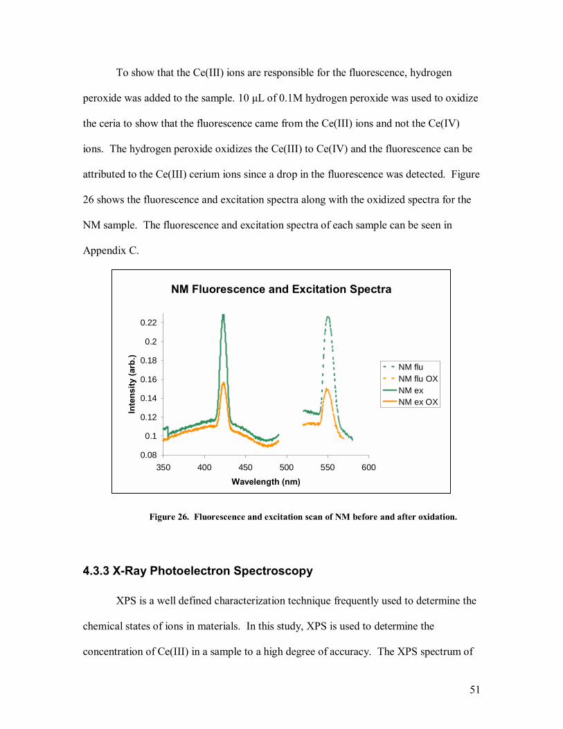
51
To show that the Ce(III) ions are responsible for the fluorescence, hydrogen
peroxide was added to the sample. 10 µL of 0.1M hydrogen peroxide was used to oxidize
the ceria to show that the fluorescence came from the Ce(III) ions and not the Ce(IV)
ions. The hydrogen peroxide oxidizes the Ce(III) to Ce(IV) and the fluorescence can be
attributed to the Ce(III) cerium ions since a drop in the fluorescence was detected. Figure
26 shows the fluorescence and excitation spectra along with the oxidized spectra for the
NM sample. The fluorescence and excitation spectra of each sample can be seen in
Appendix C.
Figure 26. Fluorescence and excitation scan of NM before and after oxidation.
4.3.3 X-Ray Photoelectron Spectroscopy
XPS is a well defined characterization technique frequently used to determine the
chemical states of ions in materials. In this study, XPS is used to determine the
concentration of Ce(III) in a sample to a high degree of accuracy. The XPS spectrum of
NM Fluorescence and Excitation Spectra
0.08
0.1
0.12
0.14
0.16
0.18
0.2
0.22
350 400 450 500 550 600
Wavelength (nm)
Inte
nsity
(arb
.)
NM fluNM flu OXNM exNM ex OX
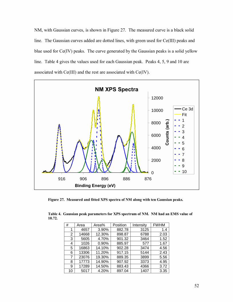
52
NM, with Gaussian curves, is shown in Figure 27. The measured curve is a black solid
line. The Gaussian curves added are dotted lines, with green used for Ce(III) peaks and
blue used for Ce(IV) peaks. The curve generated by the Gaussian peaks is a solid yellow
line. Table 4 gives the values used for each Gaussian peak. Peaks 4, 5, 9 and 10 are
associated with Ce(III) and the rest are associated with Ce(IV).
Figure 27. Measured and fitted XPS spectra of NM along with ten Gaussian peaks.
Table 4. Gaussian peak parameters for XPS spectrum of NM. NM had an EMS value of 10.72.
# Area Area% Position Intensity FWHM 1 4657 3.90% 882.78 3125 1.4 2 14668 12.30% 898.87 6788 2.03 3 5605 4.70% 901.32 3464 1.52 4 1026 0.90% 885.97 577 1.67 5 16863 14.10% 902.28 3474 4.56 6 13306 11.20% 917.15 5144 2.43 7 23076 19.30% 889.35 3899 5.56 8 17773 14.90% 907.92 3373 4.95 9 17289 14.50% 883.43 4366 3.72
10 5017 4.20% 897.04 1407 3.35
NM XPS Spectra
0
2000
4000
6000
8000
10000
12000
876886896906916Binding Energy (eV)
Cou
nts
(arb
.)
Ce 3dFit12345678910
53
According to the spectrophotometry and fluorometry measurements, NM should
have the highest amount of Ce(III) present. The amount of Ce(III) as determined by XPS
is 33.7% and the EMS value is 10.72. The Ce(III) concentration corresponds to a γ value
of 0.169. The XPS spectrum of N130, which should have the lowest amount of Ce(III)
present according to the spectrophotometry and fluorometry measurements, is shown in
Figure 57. The amount of Ce(III) in N130 as determined by XPS is 27.9% with an EMS
value of 13.8. This value corresponds to a γ value of 0.140. The Ce(III) concentration as
determined by XPS for all samples can be seen in Table 5. The Ce(III) concentrations
match up very well with the optical spectroscopy results, with Z10 having the highest
Ce(III) concentration, followed by NM having the second highest Ce(III) concentration
and N130 with the least.
To determine the amount of variation from run to run, the XPS spectrum of N160
was measured three times. The Ce(III) concentrations found were 30.6%, 31.4% and
31.5% with EMS values of 6.5, 10.12 and 10.59 respectively. The second and third
measurements, which have EMS values that differ by less than 0.5, correspond to Ce(III)
concentrations that differ by a tenth of a percent. This tiny amount of variation between
runs indicates that the run to run variation of the XPS system is negligible. The N160
spectra and all other XPS spectra can be found in Appendix D.
4.3.4 X-Ray Diffraction
XRD was performed to find the probability of a preferred orientation for the
surface planes in the ceria nanoparticles. The ratio A(111)/A(200) gives the probability that
one plane will occur predominantly in the sample. Since the 111 plane has a lower
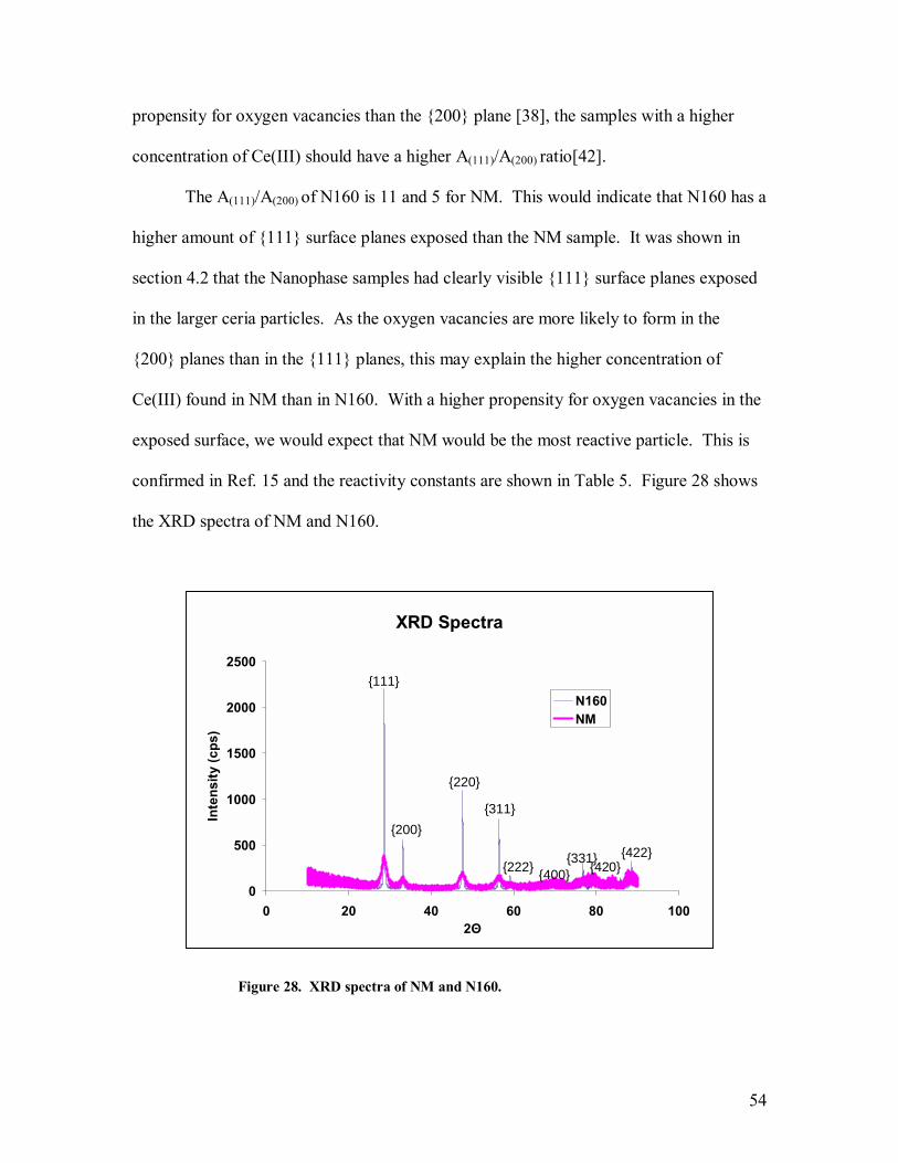
54
propensity for oxygen vacancies than the 200 plane [38], the samples with a higher
concentration of Ce(III) should have a higher A(111)/A(200) ratio[42].
The A(111)/A(200) of N160 is 11 and 5 for NM. This would indicate that N160 has a
higher amount of 111 surface planes exposed than the NM sample. It was shown in
section 4.2 that the Nanophase samples had clearly visible 111 surface planes exposed
in the larger ceria particles. As the oxygen vacancies are more likely to form in the
200 planes than in the 111 planes, this may explain the higher concentration of
Ce(III) found in NM than in N160. With a higher propensity for oxygen vacancies in the
exposed surface, we would expect that NM would be the most reactive particle. This is
confirmed in Ref. 15 and the reactivity constants are shown in Table 5. Figure 28 shows
the XRD spectra of NM and N160.
Figure 28. XRD spectra of NM and N160.
XRD Spectra
0
500
1000
1500
2000
2500
0 20 40 60 80 1002Θ
Inte
nsity
(cps
)
N160NM
111
200
220
311
222 400331420
422
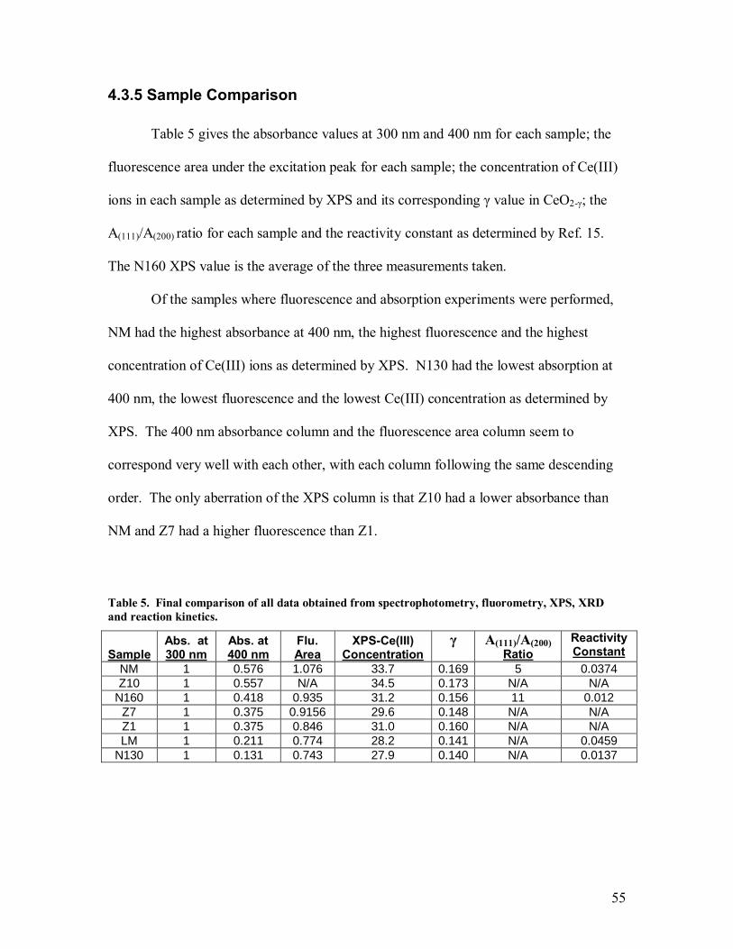
55
4.3.5 Sample Comparison
Table 5 gives the absorbance values at 300 nm and 400 nm for each sample; the
fluorescence area under the excitation peak for each sample; the concentration of Ce(III)
ions in each sample as determined by XPS and its corresponding γ value in CeO2-γ; the
A(111)/A(200) ratio for each sample and the reactivity constant as determined by Ref. 15.
The N160 XPS value is the average of the three measurements taken.
Of the samples where fluorescence and absorption experiments were performed,
NM had the highest absorbance at 400 nm, the highest fluorescence and the highest
concentration of Ce(III) ions as determined by XPS. N130 had the lowest absorption at
400 nm, the lowest fluorescence and the lowest Ce(III) concentration as determined by
XPS. The 400 nm absorbance column and the fluorescence area column seem to
correspond very well with each other, with each column following the same descending
order. The only aberration of the XPS column is that Z10 had a lower absorbance than
NM and Z7 had a higher fluorescence than Z1.
Table 5. Final comparison of all data obtained from spectrophotometry, fluorometry, XPS, XRD and reaction kinetics.
Sample Abs. at 300 nm
Abs. at 400 nm
Flu. Area
XPS-Ce(III) Concentration
γ A(111)/A(200) Ratio
Reactivity Constant
NM 1 0.576 1.076 33.7 0.169 5 0.0374 Z10 1 0.557 N/A 34.5 0.173 N/A N/A
N160 1 0.418 0.935 31.2 0.156 11 0.012 Z7 1 0.375 0.9156 29.6 0.148 N/A N/A Z1 1 0.375 0.846 31.0 0.160 N/A N/A LM 1 0.211 0.774 28.2 0.141 N/A 0.0459
N130 1 0.131 0.743 27.9 0.140 N/A 0.0137
56
Chapter 5 Conclusion
Seven cerium oxide samples were compared against each other using
spectrophotometry, fluorometry and XPS data to observe differences in Ce(III) and
Ce(IV) concentrations. The amount of Ce(III) in each sample is important because it
increases the reactivity of the particles, which may have a beneficial effect on the lifetime
of cells by reducing the concentration of ROS.
Fluorescence of the all the samples at the same concentration was measured and
NM was found to have the highest fluorescence while N130 had the least. Confirmation
that the fluorescence originated from the Ce(III) ions was shown by oxidizing the Ce(III)
to Ce(IV) in both samples and observing a drop in the fluorescence. Spectrophotometry
data was taken of the samples and the results were examined closely to determine the
optical properties of cerium oxide as a function of Ce(III) and Ce(IV) concentrations.
The Ce(IV) was the dominant ion in all the samples. CeO2, where the cerium is Ce(IV),
has a band gap of 4eV. Point defects, caused by oxygen vacancies and where the Ce ion
has been reduced from Ce(IV) to Ce(III), exist 3eV above the valence band in the CeO2
bandgap. When the absorption spectra of the samples were measured at the same
concentrations and that data was processed such that the effects of Mie scattering were
removed and the peaks normalized, the samples that absorbed much more heavily at 400
nm were found to have a higher concentration of Ce(III) ions. NM absorbed the most at
400 nm, indicating the highest concentration of Ce(III). N130 absorbed the least,
indicating the least amount of Ce(III).
The last spectroscopy method employed to determine the Ce(III) concentration
was XPS. In this study, it was determined by XPS that Z10 had the most Ce(III), NM
57
had the second most Ce(III) and N130 had the least Ce(III). The observance of Ce(III)
and Ce(IV) in the XPS spectra therefore strongly reinforces the validity of the absorption
and fluorescence results.
Finally, XRD spectra were taken in order to determine the probability of a favored
crystal surface in the particles. The XRD spectra can be used to explain why a particular
sample had a higher concentration of Ce(III) than another sample due to the 111 crystal
planes having the lowest propensity for oxygen vacancies. The NM had a lower
A(111)/A(200) ratio than N130 and N160 and this may explain why it has a higher
concentration of Ce(III) than them.
Of the samples where the optical spectroscopy was performed, it was determined
that NM had the highest Ce(III) concentration while N130 had the lowest concentration.
It was also shown that Z10 had the highest amount of Ce(III) out of all the samples. The
Ce(III) concentrations determined through absorption, fluorescence and XPS data
matched up well, with only the occasional aberration.
Chapter 6 Future Work
6.1 Spectroscopy
The spectroscopy methods discussed so far have all been defined on particles
acquired from third-party vendors, along with one sample synthesized in the lab. This
limits the degree to which the characterization methods themselves could be
characterized. Given a wider range of particles, particularly those that contain
significantly higher concentrations of Ce(III), the spectroscopy methods could be further
refined. Although this method works well, it is possible that a better understanding of the
58
composition of the ceria nanoparticles could be obtained from the analysis of the
spectrum.
6.2 Scattering
The biggest source of ambiguity in these characterization methods is the
scattering in the absorption spectrum. There are a few experiments that could be run to
further characterize the scattering in the system. Absorption spectra of agglomerated
versus non-agglomerated ceria particles could be used to determine the difference in the
scattering profile due to Mie and Rayleigh scattering. With more lab time and with better
defined particles, the assumptions that were made could be verified. Once it was known
exactly how much Rayleigh and exactly how much Mie scattering was occurring, it
would be much easier to deconvolve the absorption peaks from the scattering profile.
6.3 Synthesis
The initial thrust of this research project was to further refine the ceria synthesis
project started by Yang Xu; this changed when it was realized that there was no quick
screening method for the Ce(III) concentration of a sample. The only method available
to was to run XPS, which would be too costly and inefficient to run on every batch of
particles synthesized. This started the search for a quick screening method to determine
the concentration of Ce(III) ions in the samples and ended with the spectroscopy methods
outlined in this report; however successful the study of spectroscopy methods have been,
the synthesis project was left completely untouched.
There are a number of experiments that could be run to further refine the synthesis
process of cerium oxide. By changing synthesis factors and examining the effects caused
59
by each change, a greater control of the material properties of the particles can be
achieved.. The first major synthesis factor that could be changed is the temperature at
which the particles are synthesized. A study on the effect that temperature had on the
shape of the nanoparticles have been previously published[42]; however, no optical
measurements were performed on these nanoparticles nor was the Ce(III)/Ce(IV)
determined. The ability to adequately replicate the results would allow us to produce
particles with a wide range of sizes and examine whether there is any correlation between
nanoparticle diameter and Ce(III) concentration. Another interesting experiment would
be to examine particles synthesized in a pure oxygen environment versus a pure nitrogen
environment. This may be a way of creating particles that possess varying Ce(III)
concentrations but have similar properties, most importantly size and preferred crystal
orientation. This would be helpful to further characterize the optical spectroscopy
methods.
Polymers could also be added during synthesis to alter the normal synthesis
process. The polymers could perform a number of rolls. They could coat the particles,
acting to help repulse the particles and reduce aggregation. They could also be used to
selectively coat the particles and the growth mechanisms, potentially altering their
reactivity. If the polymer attached to the 111 plane, then the synthesis process would
continue, but growth would be halted in the 111 plane, thus leaving the 100 plane to
grow freely. This method could be used to grow selected structures, such as cubes, in
which all exposed planes are 100.
60
6.4 Dopants
Another aspect of the synthesis procedure that should be further examined is
doping the ceria particles. Studies have shown that doping the particles with gold,
gadolinium, or indium can increase their catalytic activity[44]. If proper dopants were
identified, the optical spectroscopy methods could be used to characterize the new
particles.
6.5 Oxidized Absorption Spectrum
When the hydrogen peroxide was used to oxidize the ceria, the absorbance spectra
all had a higher value at 400 nm than before they were oxidized. Since this is the
opposite effect than was expected, there is some phenomenon is going on that we have
not been able to explain. This remains an enigma and future experimentation should be
done to determine the source of these results.
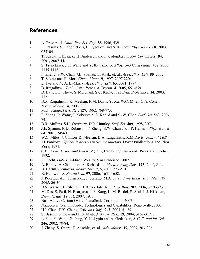
61
References
1 A. Trovarelli. Catal. Rev. Sci. Eng. 38, 1996, 439. 2 P. Patsalas, S. Logothetidis, L. Sygellou, and S. Kennou, Phys. Rev. B 68, 2003,
035104. 3 T. Suzuki, I. Kosacki, H. Anderson and P. Colomban, J. Am. Ceram. Soc. 84,
2001, 2007-14. 4 S. Tsunekawa, J.T. Wang and Y, Kawazoe, J. Alloys and Compounds. 408, 2006,
1145-1148. 5 F. Zheng, S.W. Chan, J.E. Spanier, E. Apak, et. al., Appl. Phys. Lett. 80, 2002. 6 T. Sakata and H. Mori, Chem. Mater. 9, 1997, 2197-2204. 7 L. Tye and N. A. El-Masry, Appl. Phys. Lett. 65, 3081, 1994. 8 B. Rzigalinski, Tech. Canc. Resea. & Treatm. 4, 2005, 651-659. 9 D. Bailey, L. Chow, S. Merchant, S.C. Kuiry, et al., Nat. Biotechnol. 14, 2003,
112. 10 B.A. Rzigalinski, K. Meehan, R.M. Davis, Y. Xu, W.C. Miles, C.A. Cohen.
Nanomedicine, 4, 2006, 399. 11 M.D. Sturge, Phys. Rev. 127, 1962, 768-773. 12 F. Zhang, P. Wang, J. Koberstein, S. Khalid and S.-W. Chan, Surf. Sci. 563, 2004,
74. 13 D.R. Mullins, S.H. Overbury, D.R. Huntley, Surf. Sci. 409, 1998, 307. 14 J.E. Spanier, R.D. Robinson, F. Zheng, S.W. Chan and I.P. Herman, Phys. Rev. B
64, 2001, 245407. 15 W.C. Miles, J. Clinton, K. Meehan, B.A. Rzigalinski, R.M Davis. Journal TBD 16 J.I. Pankove, Optical Processes in Semiconductors, Dover Publications, Inc. New
York, 1971. 17 C.C. Davis, Lasers and Electro-Optics, Cambridge University Press, Cambridge,
1992. 18 E. Hecht, Optics, Addison Wesley, San Francisco, 2002. 19 A. Bokov, A. Chaudhuri, A. Richardson, Mech. Ageing Dev., 125, 2004, 811. 20 D. Harman, Antioxid. Redox. Signal, 5, 2003, 557-561. 21 B. Halliwell, J. Neurochem. 97, 2006, 1634-1658. 22 J. Rodrigo, A.P. Fernandez, J. Serrano, M.A. et. al., Free Radic. Biol. Med., 39,
2005, 26-50. 23 D.S. Warner, H. Sheng, I. Batinic-Haberle, J. Exp. Biol. 207, 2004, 3221-3231. 24 M. Das, S. Patil, N. Bhargava, J. F. Kang, L. M. Riedel, S. Seal, J. J. Hickman,
Biomaterials, 28(11), 2007, 1918. 25 NanoActive Cerium Oxide, NanoScale Corporation, 2007. 26 Nanophase Cerium Oxide: Technologies and Capabilities, Romeoville, 2007. 27 H.I. Chen, H.Y. Chang, Coll. and Surf., 242, 2004, 61-69. 28 S. Basu, P.S. Devi and H.S. Maiti, J. Mater. Res., 19, 2004, 3162-3171. 29 L. Yin, Y. Wang, G. Pang, Y. Koltypin and A. Gedanken, J. Coll. and Int. Sci.,
246, 2002, 78-84. 30 J. Zhang, S. Ohara, T. Adschiri, et. al., Adv. Mater., 19, 2007, 203-206.
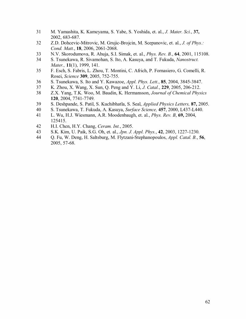
62
31 M. Yamashita, K. Kameyama, S. Yabe, S. Yoshida, et. al., J. Mater. Sci., 37, 2002, 683-687.
32 Z.D. Dohcevic-Mitrovic, M. Grujic-Brojcin, M. Scepanovic, et. al., J. of Phys.: Cond. Matt., 18, 2006, 2061-2068.
33 N.V. Skorodumova, R. Ahuja, S.I. Simak, et. al., Phys. Rev. B., 64, 2001, 115108. 34 S. Tsunekawa, R. Sivamohan, S. Ito, A. Kasuya, and T. Fukuda, Nanostruct.
Mater., 11(1), 1999, 141. 35 F. Esch, S. Fabris, L. Zhou, T. Montini, C. Africh, P. Fornasiero, G. Comelli, R.
Rosei, Science 309, 2005, 752-755. 36 S. Tsunekawa, S. Ito and Y. Kawazoe, Appl. Phys. Lett., 85, 2004, 3845-3847. 37 K. Zhou, X. Wang, X. Sun, Q. Peng and Y. Li, J. Catal., 229, 2005, 206-212. 38 Z.X. Yang, T.K. Woo, M. Baudin, K. Hermansson, Journal of Chemical Physics
120, 2004, 7741-7749. 39 S. Deshpande, S. Patil, S. Kuchibhatla, S. Seal, Applied Physics Letters, 87, 2005. 40 S. Tsunekawa, T. Fukuda, A. Kasuya, Surface Science, 457, 2000, L437-L440. 41 L. Wu, H.J. Wiesmann, A.R. Moodenbaugh, et. al., Phys. Rev. B, 69, 2004,
125415. 42 H.I. Chen, H.Y. Chang, Ceram. Int., 2005. 43 S.K. Kim, U. Paik, S.G. Oh, et. al., Jpn. J. Appl. Phys., 42, 2003, 1227-1230. 44 Q. Fu, W. Deng, H. Saltsburg, M. Flytzani-Stephanopoulos, Appl. Catal. B., 56,
2005, 57-68.
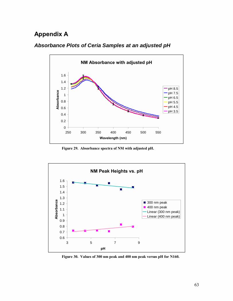
63
Appendix A
Absorbance Plots of Ceria Samples at an adjusted pH
Figure 29. Absorbance spectra of NM with adjusted pH.
Figure 30. Values of 300 nm peak and 400 nm peak versus pH for N160.
NM Absorbance with adjusted pH
0
0.2
0.4
0.6
0.8
1
1.2
1.4
1.6
250 300 350 400 450 500 550
Wavelength (nm)
Abs
orba
nce pH 8.5
pH 7.5pH 6.5pH 5.5pH 4.5pH 3.5
NM Peak Heights vs. pH
0.6
0.70.8
0.91
1.1
1.21.3
1.41.5
1.6
3 5 7 9
pH
Abs
orba
nce
300 nm peak400 nm peakLinear (300 nm peak)Linear (400 nm peak)
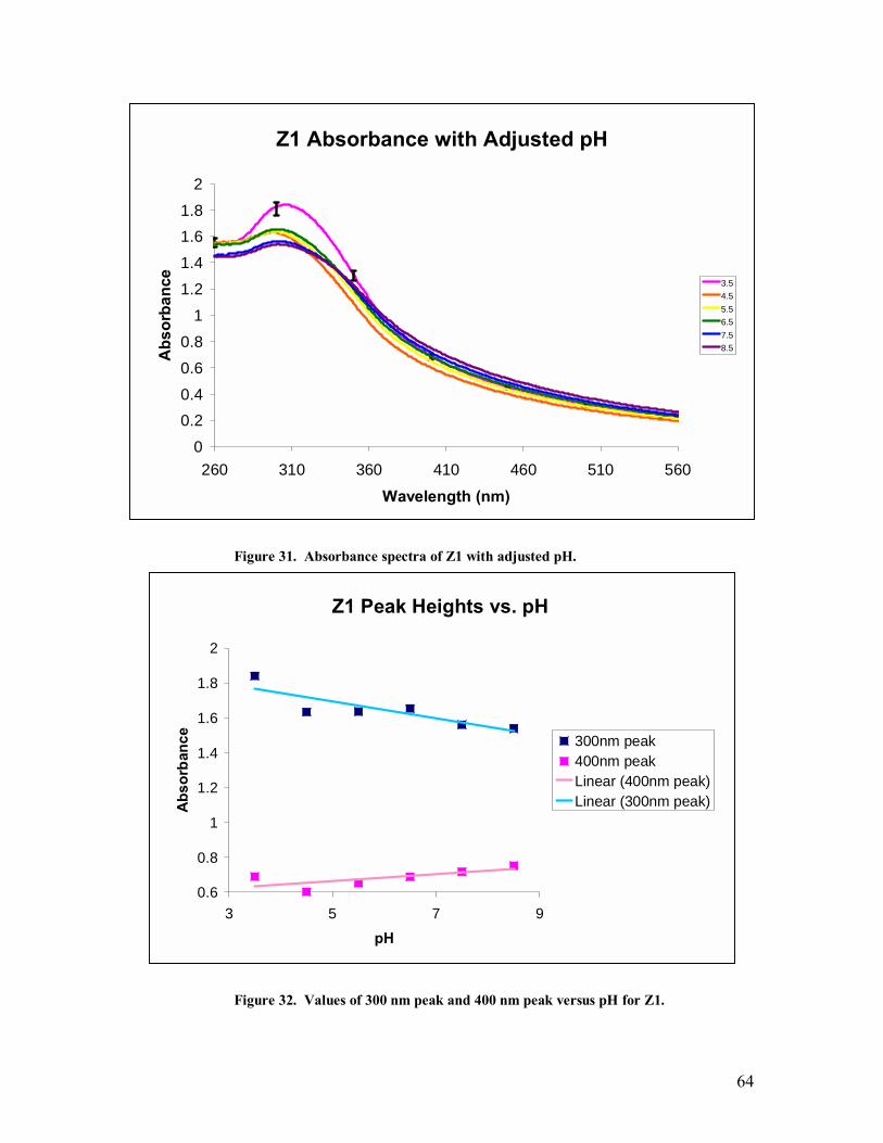
64
Figure 31. Absorbance spectra of Z1 with adjusted pH.
Figure 32. Values of 300 nm peak and 400 nm peak versus pH for Z1.
Z1 Absorbance with Adjusted pH
00.20.40.60.8
11.21.41.61.8
2
260 310 360 410 460 510 560
Wavelength (nm)
Abs
orba
nce
3.54.55.56.57.58.5
Z1 Peak Heights vs. pH
0.6
0.8
1
1.2
1.4
1.6
1.8
2
3 5 7 9
pH
Abs
orba
nce
300nm peak400nm peakLinear (400nm peak)Linear (300nm peak)
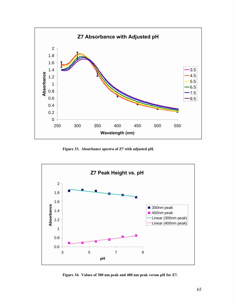
65
Figure 33. Absorbance spectra of Z7 with adjusted pH.
Figure 34. Values of 300 nm peak and 400 nm peak versus pH for Z7.
Z7 Absorbance with Adjusted pH
00.2
0.4
0.60.8
1
1.21.4
1.6
1.8
2
250 300 350 400 450 500 550
Wavelength (nm)
Abs
orba
nce 3.5
4.55.56.57.58.5
Z7 Peak Height vs. pH
0.6
0.8
1
1.2
1.4
1.6
1.8
2
3 5 7 9pH
Abs
orba
nce
300nm peak400nm peakLinear (300nm peak)Linear (400nm peak)
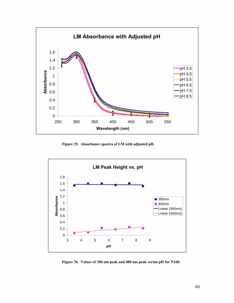
66
Figure 35. Absorbance spectra of LM with adjusted pH.
Figure 36. Values of 300 nm peak and 400 nm peak versus pH for N160.
LM Absorbance with Adjusted pH
0
0.2
0.4
0.6
0.8
1
1.2
1.4
1.6
250 300 350 400 450 500 550Wavelength (nm)
Abs
orba
nce pH 3.5
pH 4.5pH 5.5pH 6.5pH 7.5pH 8.5
LM Peak Height vs. pH
0
0.2
0.4
0.6
0.8
1
1.2
1.4
1.6
1.8
3 4 5 6 7 8 9
pH
Abs
orba
nce
300nm400nmLinear (300nm)Linear (400nm)
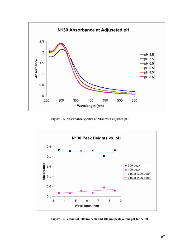
67
Figure 37. Absorbance spectra of N130 with adjusted pH.
Figure 38. Values of 300 nm peak and 400 nm peak versus pH for N130.
N130 Absorbance at Adjuseted pH
0
0.5
1
1.5
2
2.5
250 300 350 400 450 500 550Wavelength (nm)
Abs
orba
nce
pH 8.5pH 7.5pH 6.5pH 5.5pH 4.5pH 3.5
N130 Peak Heights vs. pH
0.1
0.6
1.1
1.6
2.1
2.6
3 4 5 6 7 8 9
Wavelength (nm)
Abs
orba
nce
300 peak400 peakLinear (300 peak)Linear (400 peak)
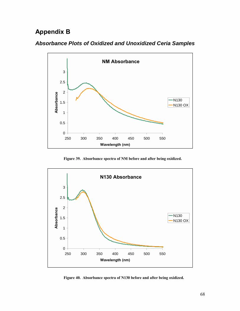
68
Appendix B
Absorbance Plots of Oxidized and Unoxidized Ceria Samples
Figure 39. Absorbance spectra of NM before and after being oxidized.
Figure 40. Absorbance spectra of N130 before and after being oxidized.
NM Absorbance
0
0.5
1
1.5
2
2.5
3
250 300 350 400 450 500 550
Wavelength (nm)
Abs
orba
nce
N130N130 OX
N130 Absorbance
0
0.5
1
1.5
2
2.5
3
250 300 350 400 450 500 550
Wavelength (nm)
Abs
orba
nce
N130N130 OX
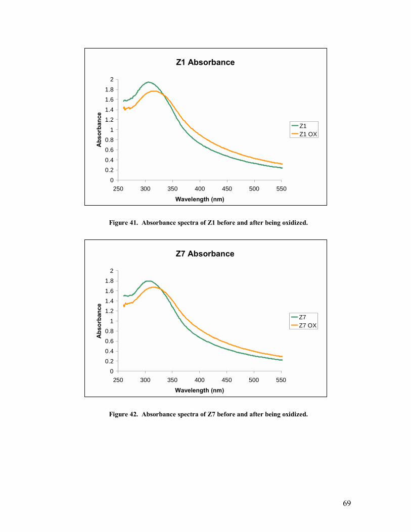
69
Figure 41. Absorbance spectra of Z1 before and after being oxidized.
Figure 42. Absorbance spectra of Z7 before and after being oxidized.
Z1 Absorbance
0
0.20.4
0.60.8
1
1.21.4
1.61.8
2
250 300 350 400 450 500 550
Wavelength (nm)
Abs
orba
nce
Z1Z1 OX
Z7 Absorbance
00.2
0.40.60.8
1
1.21.41.6
1.82
250 300 350 400 450 500 550
Wavelength (nm)
Abs
orba
nce
Z7Z7 OX
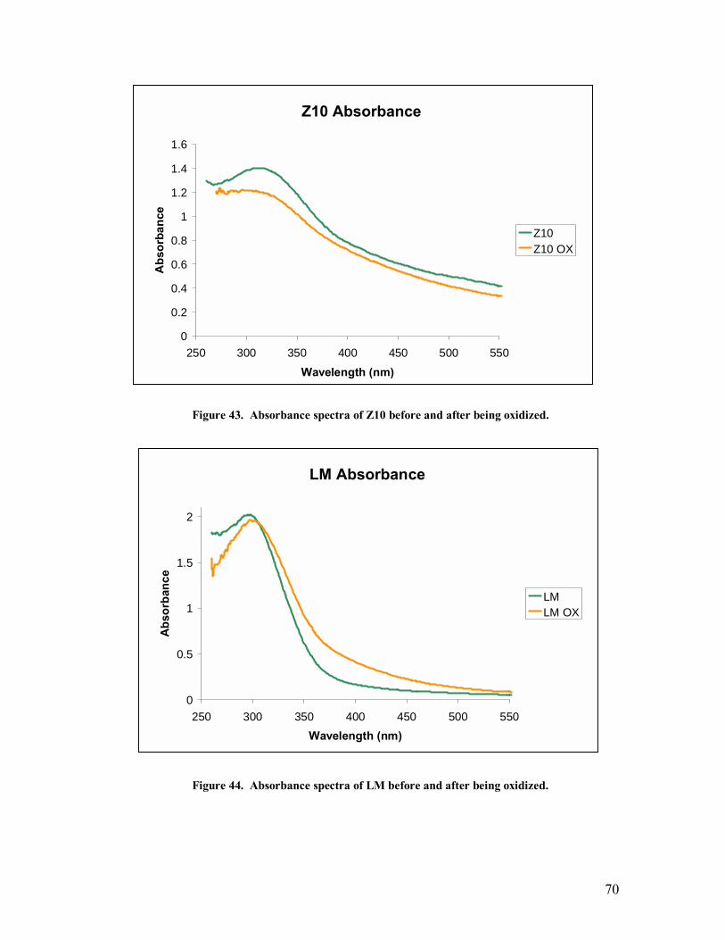
70
Figure 43. Absorbance spectra of Z10 before and after being oxidized.
Figure 44. Absorbance spectra of LM before and after being oxidized.
Z10 Absorbance
0
0.2
0.4
0.6
0.8
1
1.2
1.4
1.6
250 300 350 400 450 500 550
Wavelength (nm)
Abs
orba
nce
Z10Z10 OX
LM Absorbance
0
0.5
1
1.5
2
250 300 350 400 450 500 550Wavelength (nm)
Abs
orba
nce
LMLM OX
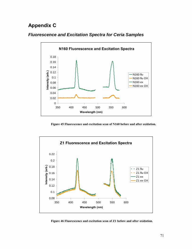
71
Appendix C
Fluorescence and Excitation Spectra for Ceria Samples
Figure 45 Fluorescence and excitation scan of N160 before and after oxidation.
Figure 46 Fluorescence and excitation scan of Z1 before and after oxidation.
N160 Fluorescence and Excitation Spectra
0
0.02
0.04
0.06
0.08
0.1
0.12
0.14
0.16
0.18
350 400 450 500 550 600
Wavelength (nm)
Inte
nsity
(arb
.)
N160 fluN160 flu OXN160 exN160 ex OX
Z1 Fluorescence and Excitation Spectra
0.08
0.1
0.12
0.14
0.16
0.18
0.2
0.22
350 400 450 500 550 600
Wavelength (nm)
Inte
nsity
(arb
.)
Z1 fluZ1 flu OXZ1 exZ1 ex OX
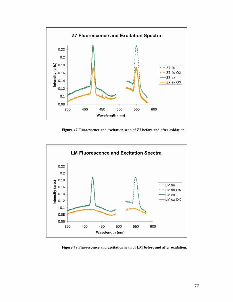
72
Figure 47 Fluorescence and excitation scan of Z7 before and after oxidation.
Figure 48 Fluorescence and excitation scan of LM before and after oxidation.
Z7 Fluorescence and Excitation Spectra
0.08
0.1
0.12
0.14
0.16
0.18
0.2
0.22
350 400 450 500 550 600
Wavelength (nm)
Inte
nsity
(arb
.)
Z7 fluZ7 flu OXZ7 exZ7 ex OX
LM Fluorescence and Excitation Spectra
0.06
0.08
0.1
0.12
0.14
0.16
0.18
0.2
0.22
350 400 450 500 550 600
Wavelength (nm)
Inte
nsity
(arb
.)
LM fluLM flu OXLM exLM ex OX
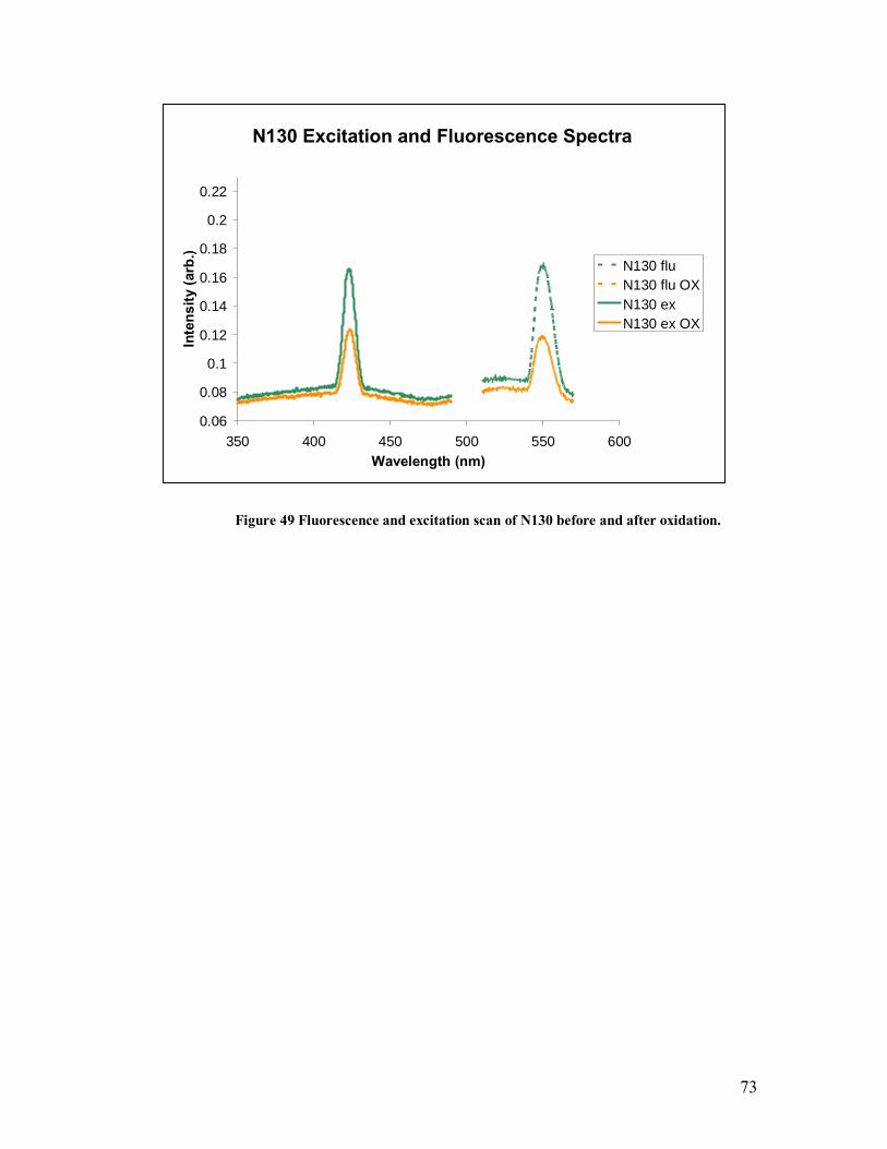
73
Figure 49 Fluorescence and excitation scan of N130 before and after oxidation.
N130 Excitation and Fluorescence Spectra
0.06
0.08
0.1
0.12
0.14
0.16
0.18
0.2
0.22
350 400 450 500 550 600Wavelength (nm)
Inte
nsity
(arb
.)
N130 fluN130 flu OXN130 exN130 ex OX
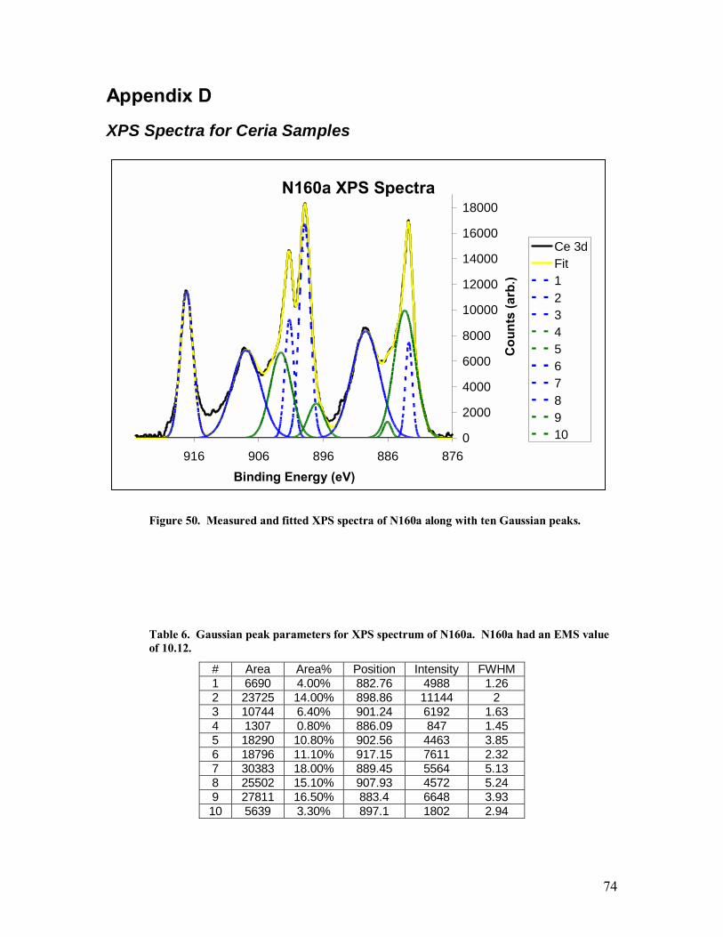
74
Appendix D
XPS Spectra for Ceria Samples
Figure 50. Measured and fitted XPS spectra of N160a along with ten Gaussian peaks.
Table 6. Gaussian peak parameters for XPS spectrum of N160a. N160a had an EMS value of 10.12.
# Area Area% Position Intensity FWHM 1 6690 4.00% 882.76 4988 1.26 2 23725 14.00% 898.86 11144 2 3 10744 6.40% 901.24 6192 1.63 4 1307 0.80% 886.09 847 1.45 5 18290 10.80% 902.56 4463 3.85 6 18796 11.10% 917.15 7611 2.32 7 30383 18.00% 889.45 5564 5.13 8 25502 15.10% 907.93 4572 5.24 9 27811 16.50% 883.4 6648 3.93 10 5639 3.30% 897.1 1802 2.94
N160a XPS Spectra
0
2000
4000
6000
8000
10000
12000
14000
16000
18000
876886896906916Binding Energy (eV)
Cou
nts
(arb
.)
Ce 3dFit12345678910
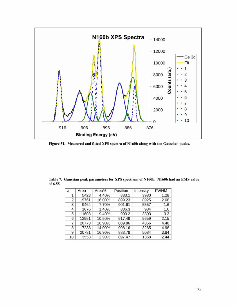
75
Figure 51. Measured and fitted XPS spectra of N160b along with ten Gaussian peaks.
Table 7. Gaussian peak parameters for XPS spectrum of N160b. N160b had an EMS value of 6.55.
# Area Area% Position Intensity FWHM 1 5423 4.40% 883.1 3980 1.28 2 19761 16.00% 899.23 8925 2.08 3 9464 7.70% 901.61 5557 1.6 4 1676 1.40% 886.3 984 1.6 5 11603 9.40% 903.2 3303 3.3 6 12951 10.50% 917.49 5659 2.15 7 20773 16.90% 889.86 4356 4.48 8 17238 14.00% 908.16 3265 4.96 9 20781 16.90% 883.78 5084 3.84
10 3553 2.90% 897.47 1368 2.44
N160b XPS Spectra
0
2000
4000
6000
8000
10000
12000
14000
876886896906916Binding Energy (eV)
Cou
nts
(arb
.)
Ce 3dFit12345678910
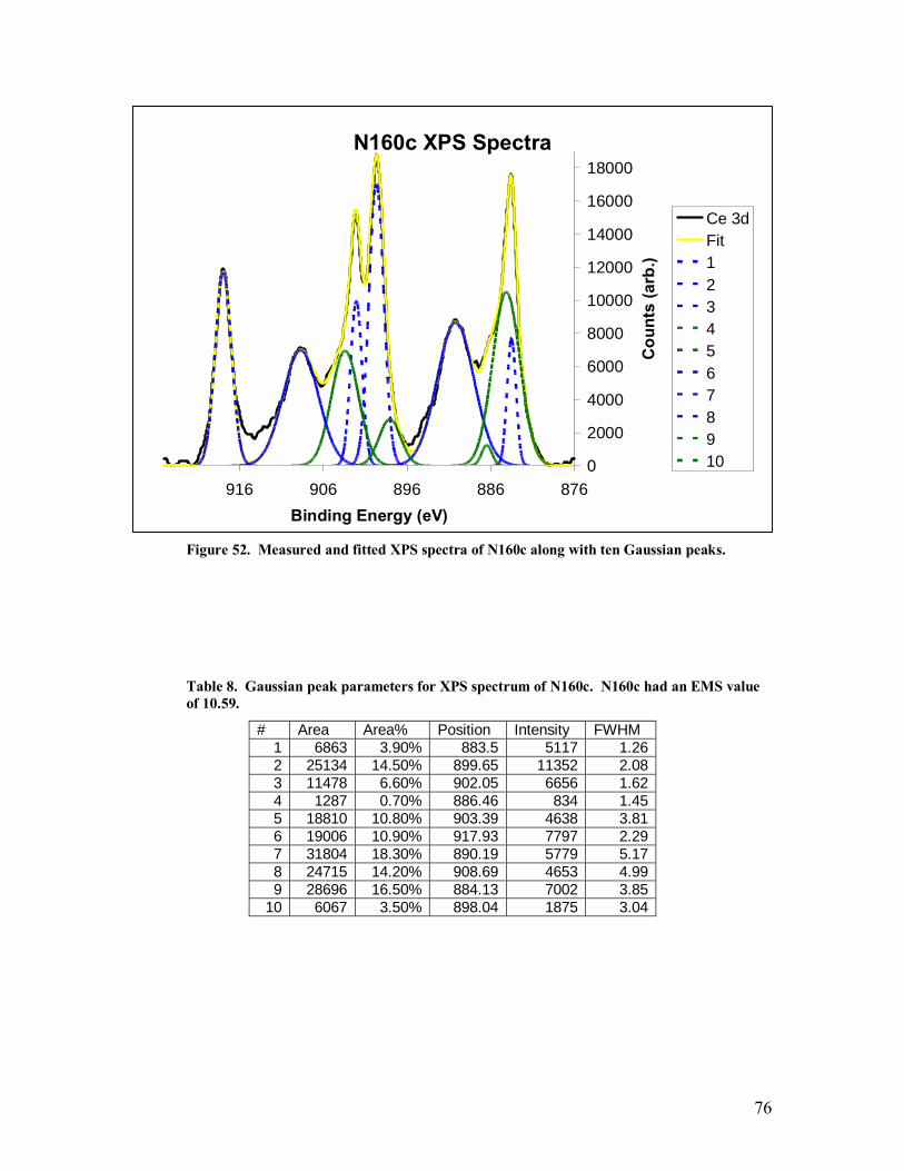
76
Figure 52. Measured and fitted XPS spectra of N160c along with ten Gaussian peaks.
Table 8. Gaussian peak parameters for XPS spectrum of N160c. N160c had an EMS value of 10.59.
# Area Area% Position Intensity FWHM 1 6863 3.90% 883.5 5117 1.26 2 25134 14.50% 899.65 11352 2.08 3 11478 6.60% 902.05 6656 1.62 4 1287 0.70% 886.46 834 1.45 5 18810 10.80% 903.39 4638 3.81 6 19006 10.90% 917.93 7797 2.29 7 31804 18.30% 890.19 5779 5.17 8 24715 14.20% 908.69 4653 4.99 9 28696 16.50% 884.13 7002 3.85
10 6067 3.50% 898.04 1875 3.04
N160c XPS Spectra
0
2000
4000
6000
8000
10000
12000
14000
16000
18000
876886896906916Binding Energy (eV)
Cou
nts
(arb
.)
Ce 3dFit12345678910
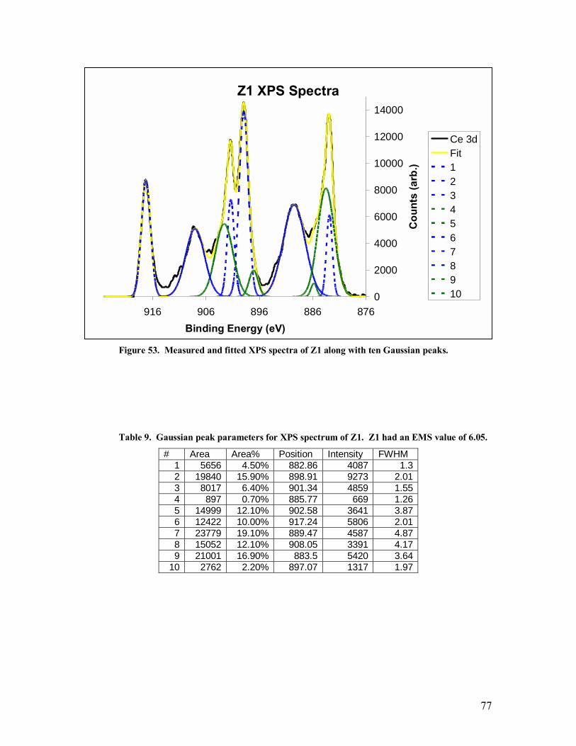
77
Figure 53. Measured and fitted XPS spectra of Z1 along with ten Gaussian peaks.
Table 9. Gaussian peak parameters for XPS spectrum of Z1. Z1 had an EMS value of 6.05.
# Area Area% Position Intensity FWHM 1 5656 4.50% 882.86 4087 1.3 2 19840 15.90% 898.91 9273 2.01 3 8017 6.40% 901.34 4859 1.55 4 897 0.70% 885.77 669 1.26 5 14999 12.10% 902.58 3641 3.87 6 12422 10.00% 917.24 5806 2.01 7 23779 19.10% 889.47 4587 4.87 8 15052 12.10% 908.05 3391 4.17 9 21001 16.90% 883.5 5420 3.64
10 2762 2.20% 897.07 1317 1.97
Z1 XPS Spectra
0
2000
4000
6000
8000
10000
12000
14000
876886896906916Binding Energy (eV)
Cou
nts
(arb
.)
Ce 3dFit12345678910
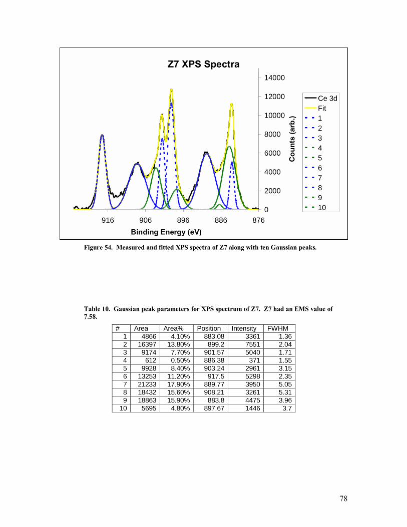
78
Figure 54. Measured and fitted XPS spectra of Z7 along with ten Gaussian peaks.
Table 10. Gaussian peak parameters for XPS spectrum of Z7. Z7 had an EMS value of 7.58.
# Area Area% Position Intensity FWHM 1 4866 4.10% 883.08 3361 1.36 2 16397 13.80% 899.2 7551 2.04 3 9174 7.70% 901.57 5040 1.71 4 612 0.50% 886.38 371 1.55 5 9928 8.40% 903.24 2961 3.15 6 13253 11.20% 917.5 5298 2.35 7 21233 17.90% 889.77 3950 5.05 8 18432 15.60% 908.21 3261 5.31 9 18863 15.90% 883.8 4475 3.96
10 5695 4.80% 897.67 1446 3.7
Z7 XPS Spectra
0
2000
4000
6000
8000
10000
12000
14000
876886896906916Binding Energy (eV)
Cou
nts
(arb
.)
Ce 3dFit12345678910
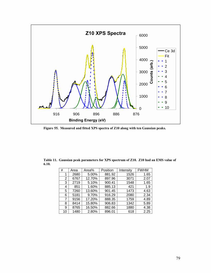
79
Figure 55. Measured and fitted XPS spectra of Z10 along with ten Gaussian peaks.
Table 11. Gaussian peak parameters for XPS spectrum of Z10. Z10 had an EMS value of 6.10.
# Area Area% Position Intensity FWHM 1 2680 5.00% 881.92 1526 1.65 2 6767 12.70% 897.96 3071 2.07 3 2719 5.10% 900.41 1548 1.65 4 851 1.60% 885.13 421 1.9 5 7260 13.60% 901.45 1473 4.63 6 5181 9.70% 916.29 2080 2.34 7 9156 17.20% 888.35 1759 4.89 8 8414 15.80% 906.83 1342 5.89 9 8765 16.50% 882.66 1880 4.38
10 1480 2.80% 896.01 618 2.25
Z10 XPS Spectra
0
1000
2000
3000
4000
5000
6000
876886896906916Binding Energy (eV)
Cou
nts
(arb
.)
Ce 3dFit12345678910
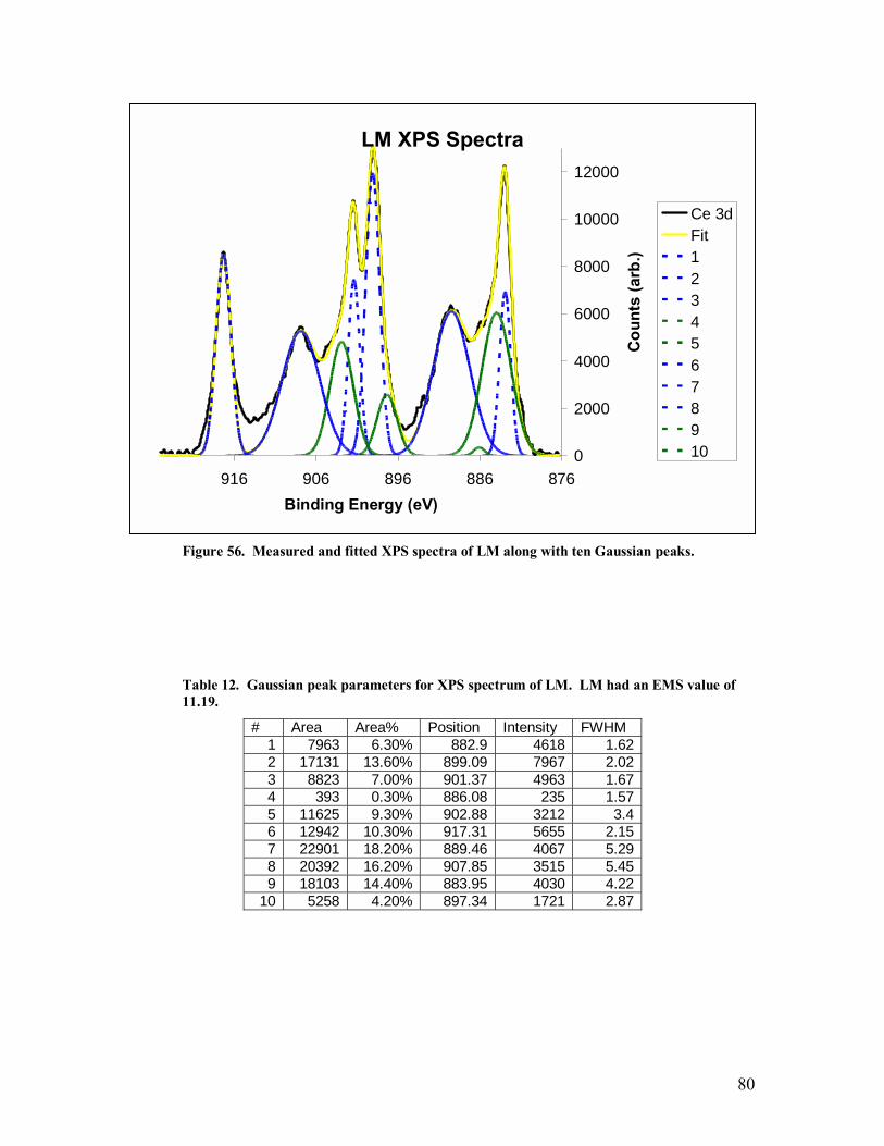
80
Figure 56. Measured and fitted XPS spectra of LM along with ten Gaussian peaks.
Table 12. Gaussian peak parameters for XPS spectrum of LM. LM had an EMS value of 11.19.
# Area Area% Position Intensity FWHM 1 7963 6.30% 882.9 4618 1.62 2 17131 13.60% 899.09 7967 2.02 3 8823 7.00% 901.37 4963 1.67 4 393 0.30% 886.08 235 1.57 5 11625 9.30% 902.88 3212 3.4 6 12942 10.30% 917.31 5655 2.15 7 22901 18.20% 889.46 4067 5.29 8 20392 16.20% 907.85 3515 5.45 9 18103 14.40% 883.95 4030 4.22
10 5258 4.20% 897.34 1721 2.87
LM XPS Spectra
0
2000
4000
6000
8000
10000
12000
876886896906916Binding Energy (eV)
Cou
nts
(arb
.)
Ce 3dFit12345678910
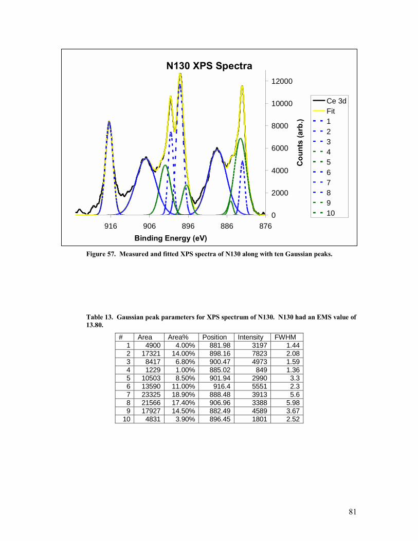
81
Figure 57. Measured and fitted XPS spectra of N130 along with ten Gaussian peaks.
Table 13. Gaussian peak parameters for XPS spectrum of N130. N130 had an EMS value of 13.80.
# Area Area% Position Intensity FWHM 1 4900 4.00% 881.98 3197 1.44 2 17321 14.00% 898.16 7823 2.08 3 8417 6.80% 900.47 4973 1.59 4 1229 1.00% 885.02 849 1.36 5 10503 8.50% 901.94 2990 3.3 6 13590 11.00% 916.4 5551 2.3 7 23325 18.90% 888.48 3913 5.6 8 21566 17.40% 906.96 3388 5.98 9 17927 14.50% 882.49 4589 3.67
10 4831 3.90% 896.45 1801 2.52
N130 XPS Spectra
0
2000
4000
6000
8000
10000
12000
876886896906916Binding Energy (eV)
Cou
nts
(arb
.)
Ce 3dFit12345678910
Recommended