International Journal of Science and Research (IJSR) ISSN (Online): 2319-7064
Index Copernicus Value (2013): 6.14 | Impact Factor (2013): 4.438
Volume 4 Issue 5, May 2015
www.ijsr.net Licensed Under Creative Commons Attribution CC BY
CNTFET Based Circuit Performance over CMOS in
Logic Gates
Mohammad Farhan
Takshshila Institute of Engineering and Technology, Jabalpur, M.P., India
Abstract: Carbon nanotubes (CNTs) exhibit high current handling capability, higher thermal and electrical conductivity and higher
transport properties, presently the Carbon nanotube technology are be the best competitor and alternative of conventionally used
Complementary metal oxide semiconductor technology(CMOS). In this paper, CNT based field effect transistors known as CNTFET is
compared with the conventionally used silicon based technology MOSFETs on the basis of circuit level performance. Those two
technologies are compared with simulation work performed on logic families such as inverter, logic gates NAND and NOR. We used gate
length of 32nm for both MOSFET and CNTFET. The results of simulation conclude that in CNTFET based logic gates, leakage power
and power delay product are lower and the delay is about 10times lower, compared to the MOSFET based devices such as logic gates.
These excellent performances characteristics with different variations are also exhibit excellent robustness.
Keywords: Carbon Nanotubes, MOSFET, CNTFET, SWNTs, VTC.
1. Introduction
The CMOS technology may posses some limitations, to
overcome these limitations we introduce the new technology
carbon nano tube technology. It have many numbers of
single walled nanotube that posses outstanding transport
capability in low voltage bias, less power consumption,
power delay and power leakage etc [1][2]. CNTFET based
devices posses these fundamental characteristics to replace
silicon based MOSFET devices. Many drawbacks are
encountered in CNTFET; these drawbacks arise under
manufacturing process like misaligned CNTs, contact
resistance and diameter problem. Now many researches
have successfully executed to supersede these drawbacks by
using accurate modeling for simulation work [3][4][5].
CNTs is a carbon allotrope that consist hollow cylinder
structure that provides a novel superior material for optimize
the electronic transport in various dimension. In modern era
of invention of micro fabrication techniques are available for
reduced the size and increase the performance of the device.
In various techniques of fabrication has pushed the
microstructure to the limit of 10 nm conviction. In other side
VLSI technology will applied for Carbon nano tube SWNTs
have a diameter below 1 nm and it is a 1D conductor [6].
That reduces the many transverse modes in compare to the
VLSI technology. Carbon nanotubes are metallic or
semiconducting based on its chirality’s and its lattice
structure gives ballistic transport properties in room
temperature. All aspects to reduce power consumption are
achieved by lowered the numbers of transistor but that
circuit is suitable only for minimum sized devices only.
Digital and analog circuits are possibly operated in the ultra
low voltage levels less than 0.4volt. This is known is
threshold region and the performance are lowered in this
region due to small energy fulfillment that will cause poor
circuit performance of standard circuits. That shows optimal
reduced energy level circuits exhibit minimum size devices
[5].
In this assessment, simulation work is done by using the
predictive technology model for a silicon based MOSFET
and HSPICE based model is used for the simulation of
CNTFET [3][4][5]. Channel length of 32nm is commonly
used for both technologies for the evaluation of the better
performance characteristics. Logic gates circuit are best
suited to determine best performing and efficient
technology.
2. MOSFET like structure of CNTFET
CNTs are sheets of graphene rolled into tubes. The single-
walled CNT can be either metallic or semiconducting just
depending on its chirality. However, the direction in which
the graphene sheet is rolled. Semiconducting nanotubes have
attracted the widespread attention of circuit designers as an
alternative channel implementation for high performance
transistors [7][8].
CNTs can be used to develop Carbon Nanotube Field Effect
Transistors (CNFETs) in which their conducting channel is
made by carbon nanotubes these are reduced in size and
gives extra ordinary electrical transfer capability with less
power loss and low power disipation. CNFETs posses less
power and intrinsic delay (CV/I), which shows higher
electron mobility compared with bulk silicon power leakage
are also less and they provide greater energy-delay product
[3]. CMOS circuit blocks are also easily replaced by them
because their operation principle is similar, so CNFET are
the best candidature to replace CMOS. The thin films of
SWNTs can potentially decrease the device-device
variations which are occurred in single tube transistors by
the statistical averaging.
Figure 1: Top view of CNTFET with multiple SWNTs. On
the other hand transistor which active conducting channel is
Paper ID: SUB154193 498
International Journal of Science and Research (IJSR) ISSN (Online): 2319-7064
Index Copernicus Value (2013): 6.14 | Impact Factor (2013): 4.438
Volume 4 Issue 5, May 2015
www.ijsr.net Licensed Under Creative Commons Attribution CC BY
aligned arrays of SWNTs are retain the high mobility as in a
SWNT transistor.
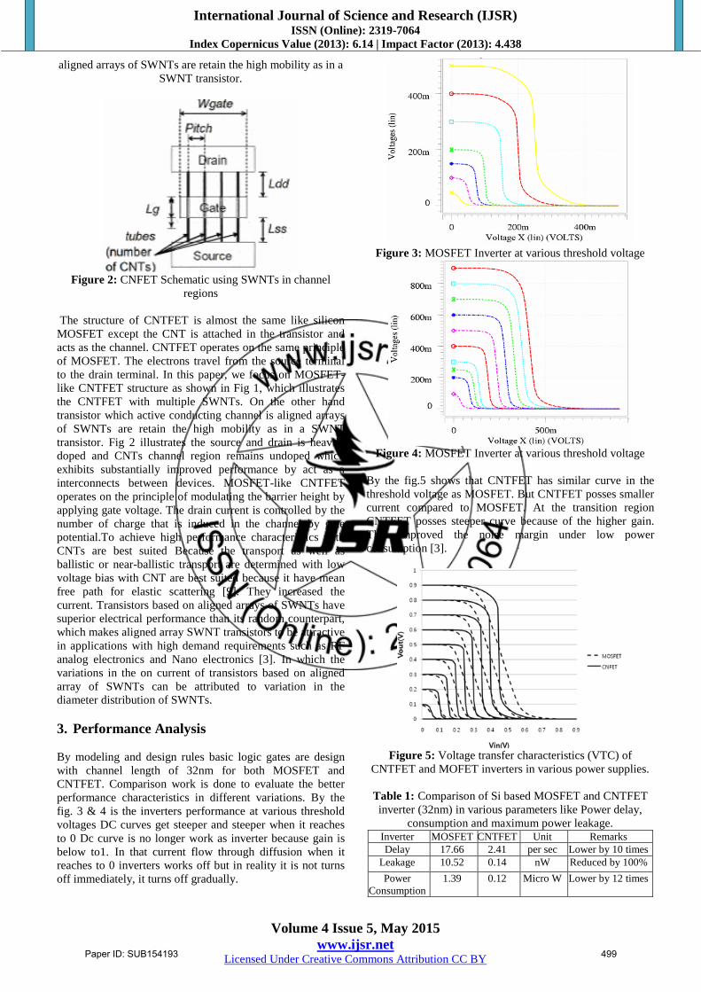
Figure 2: CNFET Schematic using SWNTs in channel
regions
The structure of CNTFET is almost the same like silicon
MOSFET except the CNT is attached in the transistor and
acts as the channel. CNTFET operates on the same principle
of MOSFET. The electrons travel from the source terminal
to the drain terminal. In this paper, we focus on MOSFET-
like CNTFET structure as shown in Fig 1, which illustrates
the CNTFET with multiple SWNTs. On the other hand
transistor which active conducting channel is aligned arrays
of SWNTs are retain the high mobility as in a SWNT
transistor. Fig 2 illustrates the source and drain is heavily
doped and CNTs channel region remains undoped which
exhibits substantially improved performance by act as a
interconnects between devices. MOSFET-like CNTFET
operates on the principle of modulating the barrier height by
applying gate voltage. The drain current is controlled by the
number of charge that is induced in the channel by gate
potential.To achieve high performance characteristics with
CNTs are best suited Because the transport as well as
ballistic or near-ballistic transport are determined with low
voltage bias with CNT are best suited because it have mean
free path for elastic scattering [9]. They increased the
current. Transistors based on aligned arrays of SWNTs have
superior electrical performance than its random counterpart,
which makes aligned array SWNT transistors to be attractive
in applications with high demand requirements such as RF
analog electronics and Nano electronics [3]. In which the variations in the on current of transistors based on aligned
array of SWNTs can be attributed to variation in the
diameter distribution of SWNTs.
3. Performance Analysis
By modeling and design rules basic logic gates are design
with channel length of 32nm for both MOSFET and
CNTFET. Comparison work is done to evaluate the better
performance characteristics in different variations. By the
fig. 3 & 4 is the inverters performance at various threshold
voltages DC curves get steeper and steeper when it reaches
to 0 Dc curve is no longer work as inverter because gain is
below to1. In that current flow through diffusion when it
reaches to 0 inverters works off but in reality it is not turns
off immediately, it turns off gradually.
Figure 3: MOSFET Inverter at various threshold voltage
Figure 4: MOSFET Inverter at various threshold voltage
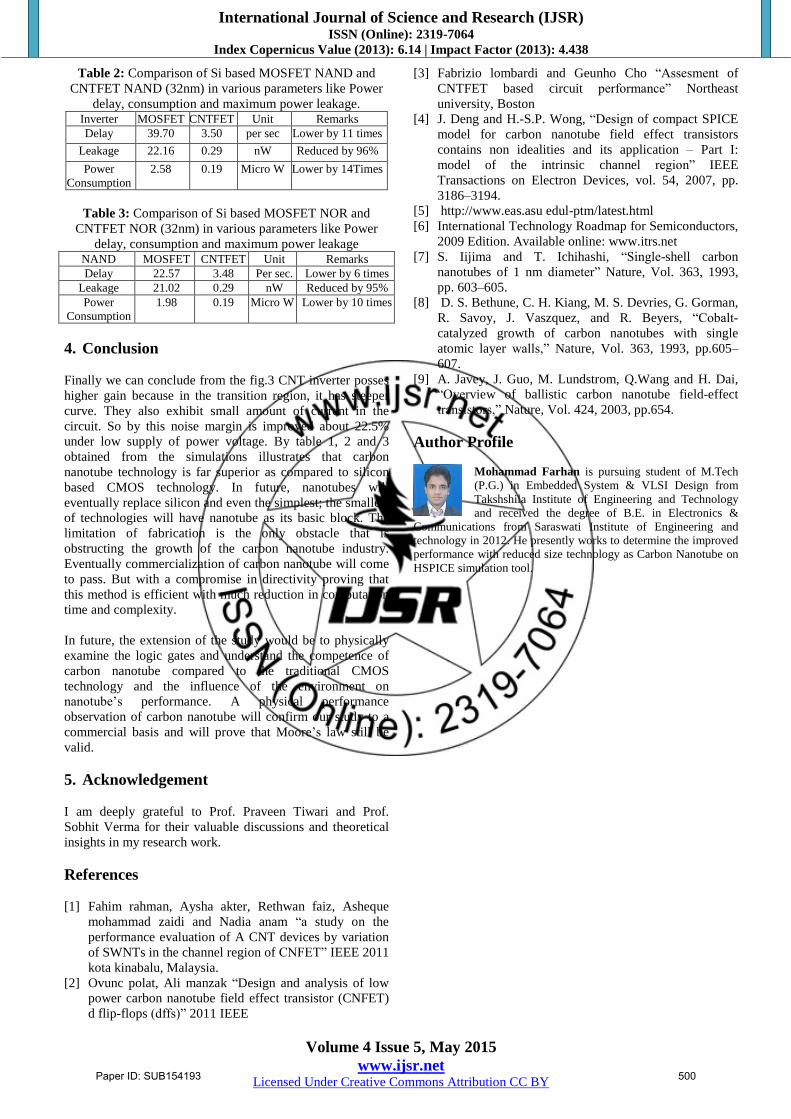
By the fig.5 shows that CNTFET has similar curve in the
threshold voltage as MOSFET. But CNTFET posses smaller
current compared to MOSFET. At the transition region
CNTFET posses steeper curve because of the higher gain.
This improved the noise margin under low power
consumption [3].
Figure 5: Voltage transfer characteristics (VTC) of
CNTFET and MOFET inverters in various power supplies.
Table 1: Comparison of Si based MOSFET and CNTFET
inverter (32nm) in various parameters like Power delay,
consumption and maximum power leakage. Inverter MOSFET CNTFET Unit Remarks
Delay 17.66 2.41 per sec Lower by 10 times
Leakage 10.52 0.14 nW Reduced by 100%
Power
Consumption
1.39 0.12 Micro W Lower by 12 times
Paper ID: SUB154193 499
International Journal of Science and Research (IJSR) ISSN (Online): 2319-7064
Index Copernicus Value (2013): 6.14 | Impact Factor (2013): 4.438
Volume 4 Issue 5, May 2015
www.ijsr.net Licensed Under Creative Commons Attribution CC BY
Table 2: Comparison of Si based MOSFET NAND and
CNTFET NAND (32nm) in various parameters like Power
delay, consumption and maximum power leakage. Inverter MOSFET CNTFET Unit Remarks
Delay 39.70 3.50 per sec Lower by 11 times
Leakage 22.16 0.29 nW Reduced by 96%
Power
Consumption
2.58 0.19 Micro W Lower by 14Times
Table 3: Comparison of Si based MOSFET NOR and
CNTFET NOR (32nm) in various parameters like Power
delay, consumption and maximum power leakage
NAND MOSFET CNTFET Unit Remarks
Delay 22.57 3.48 Per sec. Lower by 6 times
Leakage 21.02 0.29 nW Reduced by 95%
Power
Consumption
1.98 0.19 Micro W Lower by 10 times
4. Conclusion
Finally we can conclude from the fig.3 CNT inverter posses
higher gain because in the transition region, it has steeper
curve. They also exhibit small amount of current in the
circuit. So by this noise margin is improved about 22.5%
under low supply of power voltage. By table 1, 2 and 3
obtained from the simulations illustrates that carbon
nanotube technology is far superior as compared to silicon
based CMOS technology. In future, nanotubes will
eventually replace silicon and even the simplest; the smallest
of technologies will have nanotube as its basic block. The
limitation of fabrication is the only obstacle that is
obstructing the growth of the carbon nanotube industry.
Eventually commercialization of carbon nanotube will come
to pass. But with a compromise in directivity proving that
this method is efficient with much reduction in computation
time and complexity.
In future, the extension of the study would be to physically
examine the logic gates and understand the competence of
carbon nanotube compared to the traditional CMOS
technology and the influence of the environment on
nanotube’s performance. A physical performance
observation of carbon nanotube will confirm our study to a
commercial basis and will prove that Moore’s law still be
valid.
5. Acknowledgement
I am deeply grateful to Prof. Praveen Tiwari and Prof.
Sobhit Verma for their valuable discussions and theoretical
insights in my research work.
References
[1] Fahim rahman, Aysha akter, Rethwan faiz, Asheque
mohammad zaidi and Nadia anam “a study on the
performance evaluation of A CNT devices by variation
of SWNTs in the channel region of CNFET” IEEE 2011
kota kinabalu, Malaysia.
[2] Ovunc polat, Ali manzak “Design and analysis of low
power carbon nanotube field effect transistor (CNFET)
d flip-flops (dffs)” 2011 IEEE
[3] Fabrizio lombardi and Geunho Cho “Assesment of
CNTFET based circuit performance” Northeast
university, Boston
[4] J. Deng and H.-S.P. Wong, “Design of compact SPICE
model for carbon nanotube field effect transistors
contains non idealities and its application – Part I:
model of the intrinsic channel region” IEEE
Transactions on Electron Devices, vol. 54, 2007, pp.
3186–3194.
[5] http://www.eas.asu edul-ptm/latest.html
[6] International Technology Roadmap for Semiconductors,
2009 Edition. Available online: www.itrs.net
[7] S. Iijima and T. Ichihashi, “Single-shell carbon
nanotubes of 1 nm diameter” Nature, Vol. 363, 1993,
pp. 603–605.
[8] D. S. Bethune, C. H. Kiang, M. S. Devries, G. Gorman,
R. Savoy, J. Vaszquez, and R. Beyers, “Cobalt-
catalyzed growth of carbon nanotubes with single
atomic layer walls,” Nature, Vol. 363, 1993, pp.605–
607.
[9] A. Javey, J. Guo, M. Lundstrom, Q.Wang and H. Dai,
“Overview of ballistic carbon nanotube field-effect
transistors,” Nature, Vol. 424, 2003, pp.654.
Author Profile
Mohammad Farhan is pursuing student of M.Tech
(P.G.) in Embedded System & VLSI Design from
Takshshila Institute of Engineering and Technology
and received the degree of B.E. in Electronics &
Communications from Saraswati Institute of Engineering and
technology in 2012. He presently works to determine the improved
performance with reduced size technology as Carbon Nanotube on
HSPICE simulation tool.
Paper ID: SUB154193 500
Recommended