CHARACTERIZATION OF MICROSTRUCTURE, DEFECTS, AND MECHANICAL PROPERTIES OF ADDITIVE MANUFACTURED NICKEL-BASE SUPERALLOYS
by
Erica Stevens
Submitted to the Graduate Faculty of
The Swanson School of Engineering in partial fulfillment
of the requirements for the degree of
Bachelor of Philosophy
University of Pittsburgh
2015

UNIVERSITY OF PITTSBURGH
SWANSON SCHOOL OF ENGINEERING
This thesis was presented
by
Erica Stevens
It was defended on
April 7, 2015
and approved by
David Dunand, PhD, Materials Science and Engineering, Northwestern University
Ian Nettleship, PhD, Mechanical Engineering and Materials Science
Albert To, PhD, Mechanical Engineering and Materials Science
Thesis Director: Markus Chmielus, PhD, Mechanical Engineering and Materials Science
ii

Copyright © by Erica Stevens
2015
iii

Due to the excellent high-temperature performance of nickel-based superalloys and the need for
complicated geometries and simple repairs, methods of creating nickel-based superalloy parts by
additive manufacturing (AM) are currently being developed. In this study, Laser Engineered Net
Shaping (LENS) is used as the AM process to create samples, and Inconel 718 is used as the nickel-
based superalloy. LENS is an AM method that uses a laser to selectively melt metal powder, while
introducing additional powder in o rder t o add t o t he volume o f t he melt pool . This process is
commonly used for part repair; however, the processing parameters and resulting structure and
properties of t he m aterial a re not yet f ully und erstood. T his s tudy c haracterizes Inconel 718
samples f abricated us ing LENS pr inting using opt ical m icroscopy, e nergy-dispersive X -ray
spectrometry, s canning el ectron m icroscopy, electron b ackscatter d iffraction, an d V ickers
microhardness, and proposes explanations for the results based on the printing process.
CHARACTERIZATION OF MICROSTRUCTURE, DEFECTS, AND MECHANICAL
PROPERTIES OF ADDITIVE MANUFACTURED NICKEL-BASE SUPERALLOYS
Erica Stevens
University of Pittsburgh, 2015
iv

TABLE OF CONTENTS
PREFACE .................................................................................................................................. XII
1.0 INTRODUCTION ........................................................................................................ 1
1.1 BACKGROUND .................................................................................................. 1
1.1.1 Additive manufacturing ............................................................................... 1
1.1.1.1 From model to part ............................................................................... 2
1.1.2 LENS manufacturing.................................................................................... 3
1.1.3 Inconel 718 ..................................................................................................... 5
1.1.4 Thermal profile and microstructure of LENS-fabricated materials ....... 6
1.1.5 Structure-property relationship .................................................................. 7
1.1.6 Scanning electron microscopy ..................................................................... 7
1.1.6.1 Energy-dispersive X-ray spectrometry ............................................... 8
1.1.6.2 Electron backscatter diffraction .......................................................... 9
1.2 EXPERIMENT .................................................................................................. 10
1.2.1 Manufacturing details ................................................................................ 10
1.2.2 Sample details .............................................................................................. 14
1.2.3 Imaging and sample preparation .............................................................. 15
1.2.4 Microhardness ............................................................................................. 18
2.0 RESULTS AND DISCUSSION ................................................................................ 21
2.1 OBSERVATION OF DOTS WITH MICROSCOPY AND EDS .................. 21
2.1.1 Dot distribution ........................................................................................... 21
2.1.2 Compositional changes ............................................................................... 23
v

2.1.3 Identification of dots as pores .................................................................... 24
2.1.4 Pore distribution changes ........................................................................... 24
2.2 ELEMENTAL DISTRIBUTION ..................................................................... 26
2.2.1 EDS results from sample faces................................................................... 26
2.2.2 Discussion of elemental distribution.......................................................... 29
2.2.2.1 Micro-contrast analysis ...................................................................... 30
2.2.2.2 Macro-contrast analysis ..................................................................... 30
2.3 GRAIN SIZE AND DISTRIBUTION ............................................................. 31
2.3.1 EBSD of sample faces ................................................................................. 32
2.3.2 EBSD of sample cross-section .................................................................... 33
2.3.3 Discussion of EBSD on sample faces ......................................................... 36
2.3.4 Discussion of EBSD of cross-section .......................................................... 38
2.4 VICKERS MICROHARDNESS: MECHANICAL PROPERTIES ............. 39
2.4.1 Initial tests.................................................................................................... 39
2.4.2 Discussion of initial hardness tests ............................................................ 41
2.4.3 Subsequent hardness testing ...................................................................... 43
2.4.3.1 Average hardness by row ................................................................... 43
2.4.4 Discussion of subsequent hardness testing ............................................... 45
2.4.5 Hardness mapping ...................................................................................... 45
2.4.5.1 Hardness mapping on slices ............................................................... 46
2.4.5.2 Hardness mapping on cross-section .................................................. 48
2.4.6 Discussion of hardness mapping ................................................................ 49
3.0 FUTURE WORK ....................................................................................................... 52
vi

4.0 CONCLUSION ........................................................................................................... 53
APPENDIX A .............................................................................................................................. 55
BIBLIOGRAPHY ....................................................................................................................... 56
vii

LIST OF TABLES
Table 1. Build parameters for LENS-printed IN718 samples A, B, C, and D. ............................. 14
Table 2. EDS data for black spots, which contained more Al and O than the nominal composition
(wt.-%) of IN718. .......................................................................................................................... 23
Table 3. Summary of EDS compositional analysis, separated to show dim, light, and bright regions
in the compositional backscatter image on the face of each sample. ............................................ 29
Table 4. Average initial Vickers microhardness values for samples A, B, C, and D. .................. 45
viii

LIST OF FIGURES
Figure 1. Staircase effect in a part with thicker layers (left) and thinner layers (right). ................. 3
Figure 2. LENS system during printing. ......................................................................................... 4
Figure 3 . T hermal c ycles in s elect la yers o f LENS-fabricated s tainless s teel b ased o n
computational data (reprinted with permission)11........................................................................... 6
Figure 4. Schematic of build process and terminology (top view of a sample)............................ 11
Figure 5. Schematic of the build path for each layer of the sample prisms. Note: number of hatching
lines is not to scale, and contour was built as one continuous bead. ........................................... 13
Figure 6. Printing parameters for samples A, B, 2, and 1 in terms of linear energy based on varying
travel speeds. ................................................................................................................................. 15
Figure 7. JEOL JSM6610 scanning electron microscope, used for imaging and energy-dispersive
X-ray spectroscopy. ...................................................................................................................... 16
Figure 8. Philips XL 30 scanning electron microscope, used for electron backscatter diffraction.
....................................................................................................................................................... 17
Figure 9. R epresentation of hardness mapping location based on s ymmetry of the sample face.
Number of indents and indent spacings are not to scale. .............................................................. 19
Figure 10. Schematic of hardness mapping area on cross-section of sample 1. Number of indents
and indent spacings are not to scale. ............................................................................................. 20
Figure 11. T op view of IN718 sample in the as-printed (left), polished (center), and re-polished
(right) conditions. .......................................................................................................................... 21
Figure 12. Optical image at 50x of difference between hatching and contour dot distribution. .. 22
ix

Figure 13. SEM micrograph. The black spots are the same features that appear as small bright dots
in the dark field DOM image. ....................................................................................................... 23
Figure 14. Part of the cross-section of sample A, where etching revealed melt pool interfaces and
distinguished layers. ...................................................................................................................... 25
Figure 15. Backscatter electron composition image of the interface between the hatching and the
contour at 50x (above) and 330x (below). .................................................................................... 27
Figure 16. Backscatter electron c omposition i mage of a region of t he hatching i n s ample C ,
exhibiting a dendritic microstructure. ........................................................................................... 28
Figure 17. EBSD inverse pole figures for sample A (a), sample B (b), sample C (c), and sample D
(d), with accompanying color key for out-of-plane orientation. ................................................... 32
Figure 18. Grain size distribution based on EBSD data. .............................................................. 33
Figure 19. EBSD image of sample 1a, from the substrate into the sample. ................................. 34
Figure 20. G rain s ize di stribution ( area f raction) f rom t he s econd s can o f t he c ross-section of
sample 1. ....................................................................................................................................... 35
Figure 21. E BSD i nverse pol e f igured f or s amples A ( a), B ( b), C ( c), a nd D ( d), w ith
accompanying or ientation ke y and i ndications of a pproximate l ocation of h atching/contour
interface (black line) and scan direction (white line). ................................................................... 36
Figure 22. Schematic of potential grain growth due to contour overbuild. .................................. 39
Figure 23. Vickers hardness values for 5x4 grid spanning hatching and contour. Test load of 300
gf and dwell time of 10 s were used. (a) sample A, (b) sample B, (c) sample C, (d) sample D ... 40
Figure 24. Hardness values for 5x4 grid of indents made with 500 gf load and a 10 s dwell time.
(a) sample A, (b) sample B, (c) sample C, (d) sample D .............................................................. 41
x

Figure 25. Distinction of the hatching and contour hardness values for the second set of hardness
tests, with 500 gf load and 10 s dwell time. .................................................................................. 43
Figure 26. Average hardness per row for initial testing of samples A, B, C, and D. ................... 44
Figure 27. Contour map of hardness values in center slice of sample A. ..................................... 47
Figure 28. Contour map of hardness values in the top slice of sample A..................................... 48
Figure 29. Hardness mapping for cross-section of sample 1. ....................................................... 49
xi

PREFACE
I w ould l ike t o t hank t he S wanson S chool of E ngineering, M ascaro C enter f or S ustainable
Innovation (MCSI), t he Office of t he P rovost of t he University of P ittsburgh, and Dr. Markus
Chmielus for funding a portion of this work. In addition, Dr. Albert To and his group members,
including Pu Zhang, are gratefully acknowledged for their collaboration and sharing of resources
for the project.
I would like to thank all of my fellow group members for their support and help, and for
making our work enjoyable. I would l ike to specifically acknowledge the work and support of
Jakub Toman, Amir Mostafaei, Corrinne Charlton, Eamonn Hughes, and Meredith Meyer.
I also appreciate the tremendous love and support of my family and friends, who helped
me through the mental challenges of completing a thesis. In particular, I would like to recognize
the encouragement of my boyfriend, Spencer Evans, and the proofreading genius of my best friend,
Chris Dumm.
Last but not least, I would like to thank my research advisor, Dr. Markus Chmielus, for
being himself: for having an infectious love of knowledge and research, for believing in me even
when I didn’t believe in myself, for raising the bar and expecting excellent work, and for making
me excited to come to work every day.
xii
1.0 INTRODUCTION
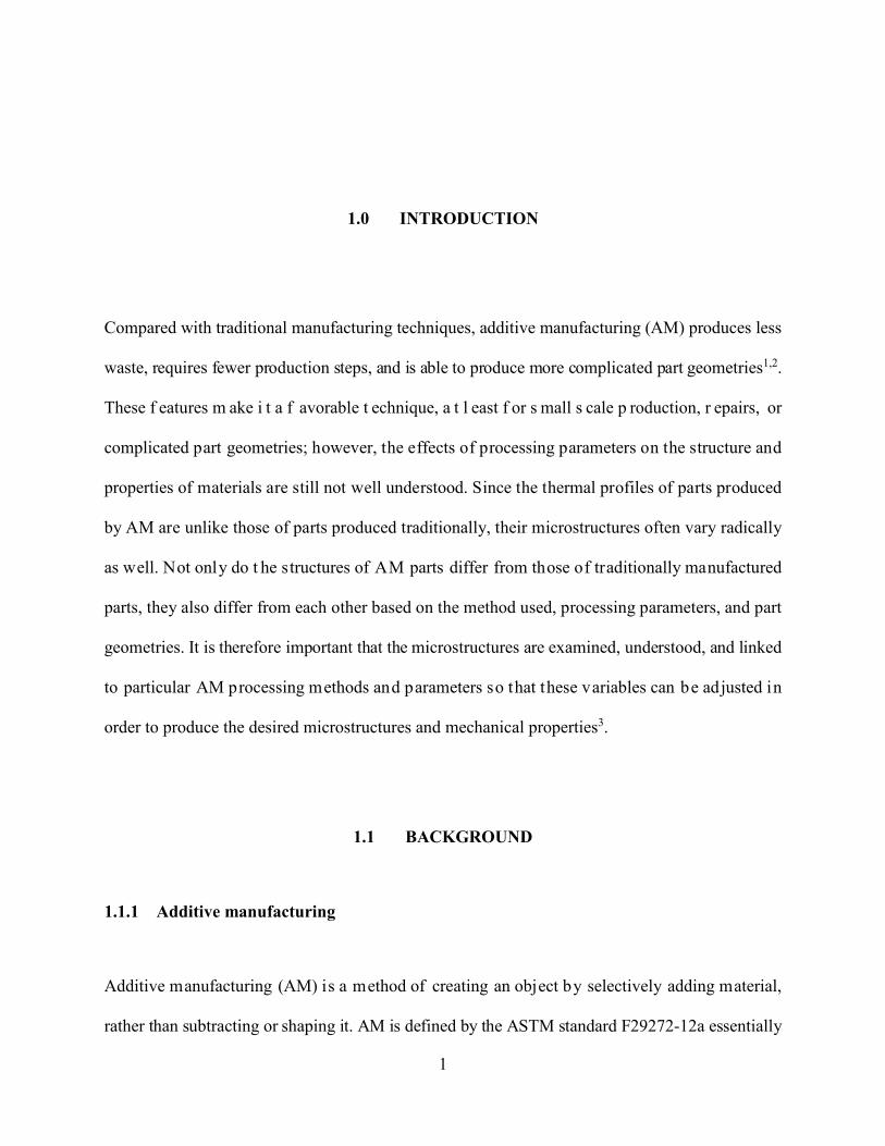
Compared with traditional manufacturing techniques, additive manufacturing (AM) produces less
waste, requires fewer production steps, and is able to produce more complicated part geometries1,2.
These f eatures m ake i t a f avorable t echnique, a t l east f or s mall s cale p roduction, r epairs, or
complicated part geometries; however, the effects of processing parameters on the structure and
properties of materials are still not well understood. Since the thermal profiles of parts produced
by AM are unlike those of parts produced traditionally, their microstructures often vary radically
as well. Not only do t he structures of AM parts differ from those of traditionally manufactured
parts, they also differ from each other based on the method used, processing parameters, and part
geometries. It is therefore important that the microstructures are examined, understood, and linked
to particular AM processing methods and parameters so that these variables can be adjusted in
order to produce the desired microstructures and mechanical properties3.
1.1 BACKGROUND
1.1.1 Additive manufacturing
Additive manufacturing (AM) is a method of creating an object by selectively adding material,
rather than subtracting or shaping it. AM is defined by the ASTM standard F29272-12a essentially
1

as the joining o f material in a manner prescribed by a 3D model, in order to create an object.
Manufacturing is typically done using one of many layer-by-layer deposition methods, in contrast
to subtractive m anufacturing and f ormative m anufacturing4,5. 3D pr inting i s of ten us ed as a
synonym for additive manufacturing, though it refers more specifically to methods that use a print
head, nozzle, or s imilar printer technology5. This paper is concerned with layer-based methods
which can be accurately referred to as 3D printing.
1.1.1.1 From model to part
In order to create an object with the desired geometry using AM, a 3D computer-aided
design (CAD) model is first created and turned into an STL file, which uses a mesh of triangles to
describe the surface geometry. Then, machine-specific AM software converts the STL file into a
slice file; it cuts the part into layers and saves the data from each layer6,7. The thickness of these
layers depends on factors such as the time available for fabrication, the accuracy of the fabrication
method, the desired accuracy of the part and machine-specific parameters7.
Due to the layering process, a curved or slanted surface which is intended to be smooth
shows instead what is often called a “staircase effect”7,8. This effect is produced when slices with
rectangular edges are stacked to create a curved or slanted surface; each layer and its contribution
to t he pa rt a re c lear, and t he s urface i s not s mooth. A s l ayer t hickness diminishes, s o do the
discontinuities resulting from the staircase effect (Figure 1)9.
2

Figure 1. Staircase effect in a part with thicker layers (left) and thinner
layers (right).
Once the slice file is created using the necessary layer thickness, it is sent to the 3D printer.
The machine creates each layer from the bottom up, printing each new layer on top of the existing
layers. Though there are many different methods that may be used to generate individual layers,
the layer-by-layer process flow itself remains the same for all layer-based 3D printers8,10.
1.1.2 LENS manufacturing
Laser engineered net shaping (LENS) is an additive manufacturing process that was developed at
Sandia National Laboratories and adapted for commercialization by Optomec4,11–13. The LENS
process takes place in a contained chamber with a constant influx of argon gas to maintain low
oxygen levels. A laser beam is first focused on a small area of solid metal, creating a melt pool.
Then, metal powders are added to the chamber through powder delivery nozzles (Figure 2). Some
land on the melt pool, becoming a part of it and adding to its volume. The laser scans over each
3

layer in a manner prescribed by a CAD model, and then proceeds on to the next layer. In this way,
a 3D part is created using layered 2D slices11–14.
Figure 2. LENS system during printing.
The LENS process has several advantages over traditional manufacturing, and even over
other 3D printing processes. LENS production creates intense thermal profiles with several cycles
of quick heating and cooling, which dictates local microstructural evolution. It is also very precise
and produces a very small heat-affected zone (HAZ). There are reported to be superior material
properties due to the microstructure created by the thermal profile, and the precision and small
HAZ are useful for selectively r epairing pa rts that would otherwise be compromised by repair
attempts15. In a ddition, t he pr ecision a bilities of LE NS allow f or t he construction of p art
geometries that would not be possible with other methods, such as complex cooling channels and
turbine pa rts12,13. Furthermore, several powder t ypes can be mixed in va rying amounts i n-situ,
allowing for small-scale, local alloying16,17.
4

1.1.3 Inconel 718
Inconel 718 ( IN718) i s a ni ckel-based superalloy, used pr imarily i n t he aerospace industry f or
high-temperature a pplications18. T he s tructure o f n ickel-based s uperalloys is p rimarily th at o f
nickel, which has an FCC crystal structure. This is beneficial for high-temperature applications
because it provides a good combination of toughness and ductility. In addition, IN718 has no phase
transformation from room temperature to the melting point, so the alloys maintain their properties
well over a large temperature range. Though nickel may not have the very best high-temperature
stability and functionality available, it is sufficient and is relatively light and inexpensive19.
IN718 in particular is often designated as a nickel-iron superalloy due to the high amount
of i ron among the alloying elements. It i s an alloy that i s commonly wrought, and therefore is
polycrystalline20. There are several main phases found in IN718: γ, γ′, γ″, and carbides and borides.
γ is the nickel-rich FCC matrix phase. γ′ and γ″ are coherent with the matrix phase, and γ″ is
preferred over γ′ in nickel-iron superalloys such as IN71819–21. γ″ is an ordered BCT phase that (in
IN718) is composed approximately of Ni3Nb and appears disc-shaped within the microstructure.
Though preferred, γ″ is much more difficult to observe in the microstructure, due to the fact that it
is nano-sized19,20,22.
IN718 is often manufactured using powder metallurgy (PM) methods because of its use in
products with complicated geometries, especially turbine parts. Therefore, in addition to repairing
turbine blades made out of IN718, LENS processing would be a useful tool for fabricating IN718
parts. It ha s t he ability t o b uild complicated p arts p recisely without a d ie and w ith litt le p ost-
processing, which greatly reduces the manufacturing cost19.
5

1.1.4 Thermal profile and microstructure of LENS-fabricated materials
LENS fabrication produces a unique thermal profile due to the focused laser scanning across the
surface of the material. Any given area of material will experience thermal cycling: hottest when
in the region of interest is inside the melt pool, cooling as the laser moves away, and heating up
again (albeit with a smaller temperature gradient) when the next layer is built on top of it (Figure
3)23.
Figure 3. Thermal cy cles within L ENS-fabricated samples, b ased o n
computational data plot from Manvatkar et al11. Time and temperature for
cycles will depend on printing process parameters.
This cycling continues with subsequent layers, with a general decreasing trend, producing
a c olumnar and de ndritic m icrostructure11,18,24. Also know n a s c ells, t hese c olumnar features
exhibit micro-segregation; the concentration of various e lements di ffers from the i nside of t he
6

feature to the outside11,25. Micro-segregation occurs because diffusion cannot occur fast enough to
homogenize the material before it solidifies26.
1.1.5 Structure-property relationship
The microstructures of materials directly affect their mechanical properties. It has been reported
that the properties of LENS-fabricated materials are generally comparable o r superior to those
produced b y t raditional manufacturing13,25,27–29. The f avorable pr operties r esult f rom the f ine
microstructure created d uring r apid s olidification. H owever, s ince t he t hermal pr ofile of ea ch
section of the part is not identical (e.g. the higher the layer, the lower the amount of thermal cycles),
the mechanical properties will vary throughout the part. As the part builds higher, it is unable to
lose heat as quickly to the substrate, the cooling rate decreases, and the cell spacing and grain size
increase acco rdingly. Larger cell s pacing has b een found t o c orrespond t o a de crease i n
hardness11,30.
1.1.6 Scanning electron microscopy
The scanning electron microscope (SEM) uses a beam of electrons directed at a specimen to obtain
a surface image or to compositional information31. It is beneficial to use an SEM when a greater
depth of field or a higher magnification than is possible with optical microscopy is required. Often
SEM is preferred over transmission electron microscopy due to the simpler sample preparation.
As i ts n ame s uggests, the s canning el ectron microscope creates an i mage b y s canning i n
consecutive lines called raster. A slower scanning speed allows for a higher resolution image to be
obtained. Three signals that can be detected using an SEM are secondary electrons, X-rays, and
7

backscattered electrons. Secondary electrons are used to create a secondary electron image, which
is used to examine topography. X-rays are used in energy-dispersive X-ray spectroscopy (EDS),
which i s a lso explained below. Backscattered el ectrons have m any uses, one being t o cr eate a
backscatter electron composition (BEC) image, where contrast arises from difference in atomic
weights (heavier elements appear b righter, corresponding to a greater number o f backscattered
electrons). Backscattered electrons are also used in electron backscatter diffraction (EBSD), which
is explained below31.
1.1.6.1 Energy-dispersive X-ray spectrometry
Energy-dispersive X-ray spectrometry (EDS) is a compositional analysis tool used within
the S EM. A s th e electron b eam in teracts w ith th e s ample, o ne o f th e r esulting s ignals is
characteristic X-rays, which are emitted when an excited outer shell electron jumps to a vacancy
in the inner shell31. EDS uses these characteristic X-rays to determine which elements are present
and in what amounts.
A c ommon E DS de tector c onsists of a c ooled semiconductor be hind a t hin be ryllium
window, surrounded with a gold film. It is known that the number of electron-hole pairs created
by a given i ncoming X -ray phot on i s pr oportional t o t hat phot on’s e nergy. W hen a vol tage i s
applied t o t he de tector, current f lows as X -rays are d etected. T he m agnitude o f t he cu rrent i s
indicative of the energy of the incoming X-ray, and can therefore be used to identify the element
that produced the X-ray31,32.
Each X-ray photon creates a pulse of current, which is analyzed and registered in the correct
energy range (channel). The result of this analysis is a h istogram which increases in resolution
with an increased amount of channels within the same energy range. Identification of elements is
done either automatically by the computer or by selecting known elements, which are then marked
8

on the histogram by a vertical line at the appropriate energy31. Sometimes however, when elements
are v ery close t ogether i n energy, i t c an be di fficult t o di stinguish be tween their p eaks on the
histogram.
1.1.6.2 Electron backscatter diffraction
Electron backscatter diffraction (EBSD) is a diffraction method which uses backscattered
electrons to determine crystallographic information. The backscattered electron coefficient (η) is
the amount of backscattered electrons emitted per incident electron. This gives rise to an effect
called electron channeling, since the backscattered electron coefficient is affected by the position
of a given crystal in relation to the incident beam. The contrast that is caused by the varying amount
of escaping backscattered electrons is therefore called channeling contrast, and it is typically very
weak. A good de tector a nd i deal s ample pr eparation a nd m icroscope c onditions a re ne eded t o
obtain a diffraction pattern31,33.
As wi th X -ray di ffraction, B ragg’s Law governs t he pa tterns t hat a re s een due t o
constructive an d d estructive i nterference i n E BSD31. B ragg’s Law s tates t hat c onstructive
interference occurs when nλ = 2d·sinθ, where n is an integer, λ is the incident wavelength with an
incident angle of θ, and d is the interplanar spacing within the crystal34. Each set of planes which
satisfies the Bragg condition diffracts in Kossel cones. These cones of diffracted electrons radiate
out at a w ide an gle and t herefore a re e ssentially two p arallel s traight lin es w hen th ey h it th e
phosphor screen detector, which then emits light. This resulting set of two lines is called a Kikuchi
band. A full EBSD pattern contains many bands, which reflect the crystal’s symmetry, as well as
the spacing of atoms in the plane, and the angles between planes33.
Due to the fact that EBSD patterns are collected from only the surface of the sample (~50
nm), sample preparation and surface quality is extremely important. Any contamination, residue,
9

or s light d eformation will decrease th e quality o f the scan. In order t o o btain excellent EBSD
patterns, one or several of the following techniques is recommended (depending on the material):
vibratory polishing, electropolishing, chemical etching, or ion etching33.
1.2 EXPERIMENT
Two sets of IN718 samples were prepared. The f irst set of four samples varied the laser t ravel
speed and software layer height. A second set of samples was prepared by varying the linear energy
using a change in the scanning speed with a constant laser power.
1.2.1 Manufacturing details
Both sets of samples were made using an Optomec LENS 450 system. Each sample was a prism
of approximately 10 mm x 10 mm x 3-5 mm and was printed in 10 layers. Each layer was printed
by first building the contour, the outside edge. After this square frame was created, the middle was
filled in by the laser scanning back and forth in parallel lines to create what is referred to as the
hatching. These lines were made at 0˚ in the first layer, 45˚ in the second layer, 90˚ in the third,
135˚ in the fourth, and so on. The hatching overlapped the contour slightly, meaning that the
contour got overbuilt and became higher than the hatching of the same layer. A schematic of the
build process and terminology can be seen in Figure 4.
10

Figure 4. Schematic of b uild p rocess an d t erminology (top vi ew of a
sample).
A s chematic of t he bui ld pa th f or e ach l ayer i s g iven i n Figure 5. For t he pur poses of
describing the details of the manufacturing process, the side of the stage and substrate that was
oriented closest to the viewing window will be referred to as the front, the side furthest from the
window as the back, the side towards the right when facing the viewing window as the right, and
the remaining side as the left.
First, the system zeroed in the back right corner of the sample, without starting the laser.
Then, the laser was oriented over the start point of the contour and was turned on automatically.
Though the contour start points were consistent between samples in corresponding layers, there
was no pa ttern to their location between layers of the same sample. In one continuous bead of
material, th e o utline, or contour, of t he m aterial w as bui lt. T he bui ld di rection of t he c ontour
alternated between clockwise and counterclockwise. After the contour was complete, the system
turned off the laser, positioned itself over the start point of the hatching, and turned the laser back
on again. As with the contour starting points, the starting points of the hatching were consistent,
though with no pattern between layers. After each individual hatching line was complete, the laser
11

turned off, the system moved over slightly to the beginning of the next hatching line, and the laser
turned on again. At the end of the hatching, the laser turned off, returned to the zero point in the
back right corner, and began the next layer in the same way.
12
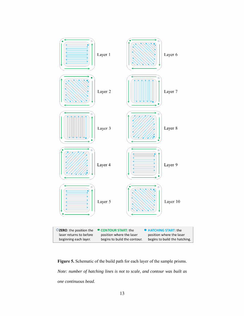
Figure 5. Schematic of the build path for each layer of the sample prisms.
Note: number of hatching lines is not to scale, and contour was built as
one continuous bead.
13

1.2.2 Sample details
The first set of samples consisted of four samples, labelled A, B, C, and D, and were made on an
IN718 s ubstrate w ith IN718 pl asma r otating e lectrode pr ocess ( PREP) powder of 44 -150 µ m
diameter. A laser power of 250 W and a hatch distance of 0.254 mm were used. Additional details
on the build parameters can be found in Table 1.
Table 1. Build parameters for LENS-printed IN718 samples A, B, C, and D.
Laser travel speed
2 mm/s 2.27 mm/s
Layer height in software 0.254 mm A B
0.203 mm C D
The second set of samples consisted of two samples, labelled 1 a nd 2. T hese were also
made on an IN718 substrate with IN718 PREP powder of 44-150 µm diameter. Laser power and
hatch d istance r emained t he s ame as f or t he f irst s et o f s amples (250 W a nd 0.254 m m,
respectively). Layer height in the software was maintained at 0.254 mm, and only the laser travel
speed was changed. This created a varying linear energy, which is equal to the laser power divided
by the laser travel speed. For sample 1, the travel speed was 5 mm/s, resulting in a 50 J/mm linear
energy. F or s ample 2, t he t ravel s peed w as 3.3 3 m m/s, r esulting i n a 7 5 J /mm linear en ergy.
Samples A and B had linear energies of 125 J/mm and 110 J/mm, respectively. These parameters
are shown in Figure 6.
14

Figure 6. Printing parameters for samples A, B, 2, and 1 in terms of linear
energy based on varying travel speeds.
1.2.3 Imaging and sample preparation
Each sample was imaged in the as-printed condition using a Keyence digital optical microscope
(DOM) with a dark field Z20 lens and a multi-diffused adapter or focal distance adapter at varying
magnifications. After the initial structure was documented, the samples were separated by using a
metallographic saw to cut the substrate around each prism. This resulted in separate samples: small
pieces of s ubstrate, each t opped w ith one of t he pr isms. Each o f t hese p ieces w as t hen h ot
compression mounted, ground, and polished. Phenolic resin was used as the mounting material for
the first set of samples, and graphite powder was used for the second set of samples due to the
benefits of having conductive mounting during electron microscopy. The progression of SiC paper
used for grinding was 400-, 600-, 800-, and 1200-grit. Final polishing was accomplished using a
0.5 µm Al2O3 suspension followed by a 0.05 µm Al2O3 suspension. After polishing, the samples
15

were examined and imaged again with the DOM in bright field and dark field, with both Z20 and
Z100 lenses.
Samples A, B, 1, and 2 were cut in half using a metallographic saw in order to access the
cross-section. The cross-sections were polished in the same way as outlined above. The cross-
section o f s ample A was s wabbed f or 10 s econds w ith Waterless K alling’s E tchant to r eveal
features of the microstructure (Number 94 in ASTM E40735).
In addition to an optical microscope, each polished sample was examined using a J EOL
JSM6610 scanning electron microscope (SEM). Images were taken using both secondary electrons
and ba ckscatter e lectrons w ith a c ompositional contrast. T he S EM w as a lso us ed t o c ollect
compositional data using energy-dispersive X-ray spectrometry (EDS) and grain distribution data
using electron backscatter diffraction (EBSD). EDS was done on the JEOL JSM6610 (Figure 7)
in the form of point scans and line scans.
Figure 7. JEOL JSM6610 scanning electron microscope, used for imaging
and energy-dispersive X-ray spectroscopy.
16

The point scans were done for 30 seconds in each of the distinct regions in a backscatter
image (e.g. dark, l ight, dim, and bright). Line scans were done for approximately 200 seconds
across regions of distinct contrast in a compositional backscatter image. EBSD was done at 50x
magnification, an 18 mm working distance, an accelerating voltage of 25 keV, and a spot size of
5 on a Philips XL 30 (Figure 8).
Figure 8. Philips XL 30 scanning electron microscope, used for electron
backscatter diffraction.
On the faces of samples A, B, C, and D, EBSD was performed in regions that spanned both
hatching and contour, with a square grid scan of 1500 µm x 1500 µm and a step size of 0.5 µm.
EBSD was also done on the cross-section of sample 1, f rom the substrate up through almost the
top layer of the sample. EBSD of the cross-section of sample 1 was done in two separate scans due
to time and area restrictions when at 50x. The first scan was 900 µm x 1800 µm with a 0.3 µm step
size and began in the substrate and extended approximately 1.28 mm into the sample. The second
17

scan was 900 µm x 1800 µm with a 0.3 µm step size and was taken overlapping the first area, and
extended an additional 0.6 mm towards the top of the sample. In total, the sample area scanned
was c lose to 1.8 m m, which i s near the total sample height of 2.1 m m. The interface with the
mounting material was unable to be scanned due to its interference with Kikuchi pattern formation.
1.2.4 Microhardness
Mechanical p roperties w ere assessed with a Leco h ardness t ester via Vickers m icrohardness
measurements with a load of 300 or 500 gf and a dwell time of 10 s . Two grids of indents were
made on each sample face, placed to sample the contour as well as the hatching. More densely-
packed indents were made on t he top and middle slices of sample A in order to obtain a m ore
comprehensive mapping of hardness values.
Hardness maps were created for the top and center slices of sample A, as well as for the
cross-section of sample 1. Indents for mapping were made with 500 gf and a 10 s dwell time, and
were placed 200 µm apart (center-to-center). The grids parallel to the substrate, which were created
on the top and center slices, were approximately rectangular, spanning one quarter of the sample
face area (Figure 9).
18
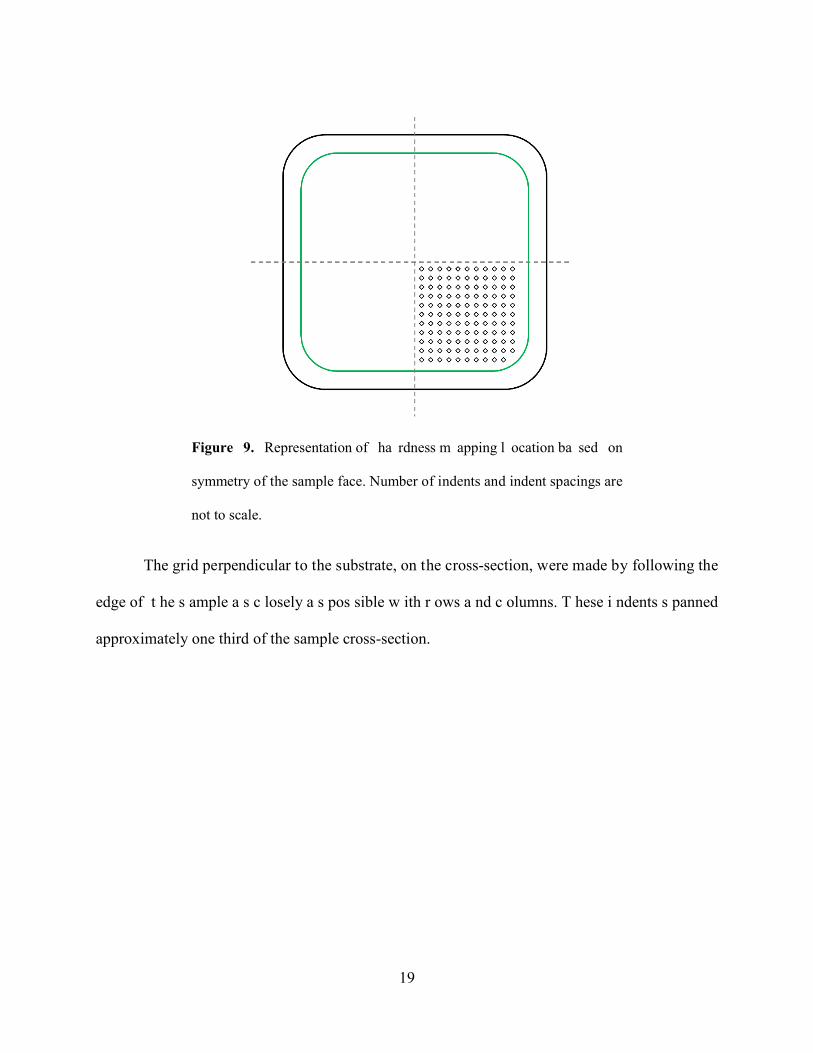
Figure 9. Representation of ha rdness m apping l ocation ba sed on
symmetry of the sample face. Number of indents and indent spacings are
not to scale.
The grid perpendicular to the substrate, on the cross-section, were made by following the
edge of t he s ample a s c losely a s pos sible w ith r ows a nd c olumns. T hese i ndents s panned
approximately one third of the sample cross-section.
19

Figure 10. Schematic o f hardness m apping ar ea o n c ross-section o f
sample 1. Number of indents and indent spacings are not to scale.
Indent size was measured using two different microscopes: the Olympus BX-60M optical
and t he K eyence di gital opt ical m icroscope. T he O lympus r equires t hat t he us er i ndicate t he
diagonals of the indent, from which it automatically calculates the hardness using parameters that
the user specifies. Based on microscope availability, the Keyence was also used to make indent
measurements. T he K eyence d oes n ot cal culate hardness au tomatically, so each d iagonal w as
measured and the averages for each indent were used in the Vickers microhardness formula (HV
= 1854.4P/d2) to calculate hardness, where P represents the applied load in gf and d represents the
average diagonal length in μm36,37.
20

2.0 RESULTS AND DISCUSSION
The r esults obt ained i ncluded opt ical m icroscopy i mages, S EM i mages, E DS/EBSD da ta, a nd
Vickers microhardness data.
2.1 OBSERVATION OF DOTS WITH MICROSCOPY AND EDS
2.1.1 Dot distribution
Figure 11 shows the top view of one of the IN718 samples in the as-printed, pol ished, and re-
polished condition.
Figure 11. Top view of IN718 sample in the as-printed ( left), polished
(center), and re-polished (right) conditions.
There were t wo t ypes of dot s vi sible: l arge (20-30 µ m) a nd s mall (<10 µ m). T he
distribution of the large dots was not affected by location in the sample. The distribution of the
21

small dots, however, were dependent on the location in the sample. In the intralayer region, the
dot distribution in the hatching followed the scan direction of the laser; in the interlayer region,
the dots were more densely packed and randomly distributed. In addition, the dots in the contour
region were consistently densely packed and randomly distributed (Figure 12).
Figure 12. Optical image at 50x of difference between hatching and
contour dot distribution.
The dots were seen in the SEM image in Figure 13 as black spots.
22

Figure 13. SEM micrograph. The black spots are the same features that
appear as small bright dots in the dark field DOM image.
2.1.2 Compositional changes
Chemical composition of the dark spots was identified with EDS. Examples of spectra are given
in Table 2 and compared to t he expected nominal composition of IN718. As compared to t he
expected compositions of 0 wt.-% O and 0.5 wt.-% Al, the spots showed an increase to between 9
and 19 wt.-% O and between 1 and 5 wt.-% Al.
Table 2. EDS data for black spots, which contained more Al and O than
the nominal composition (wt.-%) of IN718.
O Al Ti Cr Fe Ni Nb
Spot 1 18.32 4.04 1.22 15.25 13.47 38.80 8.90
23

Spot 2 9.24 1.12 1.50 16.06 14.31 46.04 11.74
Spot 3 14.20 4.26 0.93 17.52 14.83 43.12 5.14
Nominal 0 0.5 0.9 19 18.5 52.5 5.1
2.1.3 Identification of dots as pores
As there are numerous phases and the possibility for inclusions within the sample, the dots were
not immediately identified as pores, though they appeared as such based on the reflection of light
in DOM. To confirm that the dots were pores, sonication of the initial samples after polishing was
performed for only a short amount of time so that results from EDS could be examined for trapped
polishing s lurry. T he d ots s howed e levated amounts of A l a nd O c ompared t o t he nom inal
composition, though the other elements in IN718 were still detectable. This information led to the
conclusion that each dot was a hole, or pore, and that the interaction area of the electrons in EDS
allowed the elements within the bulk IN718 material to be seen. Within the pore was remnants of
polishing slurry consisting of Al2O3, explaining the presence of anomalous levels of Al and O.
2.1.4 Pore distribution changes
When the sample was first polished, the face was a part of the top layer deposited. After being
ground and polished again, enough material was removed to expose the interface between the top
layer and the one directly beneath it. This can be determined from the view of the cross-section of
sample A (Figure 14), which was polished to a plane that was still within the tenth layer. In Figure
24

14, the top face is clearly still within the top layer, but could feasibly be polished down enough to
expose the interface.
Figure 14. Part of the cross-section of sample A, where etching revealed
melt pool interfaces and distinguished layers.
The scanning lines that are seen in Figure 11 were a result of the edges of melt pools, which
can also be identified in Figure 14, the cross-section. The edges of the melt pools have an increased
number of pores. In the top view and in the middle of a layer, these edges and their contained pores
trace out the scan direction, though they do not exactly reflect the laser’s path since the scan lines
overlap each other. When the sample was polished to a depth which exposed an intralayer surface,
the bottom of the upper melt pools met with the top of the lower melt pools, and caused a much
denser and more random distribution of pores.
The di fference be tween t he di stribution i n the c ontour a nd t he ha tching c an be e xplained i n a
similar way. Since the contour was built first in every layer and then the hatching was built with
some overlap, there is more re-melting and more interaction between edges of melt pools in the
25

contour t han i n t he ha tching. Therefore, t here is e xpected t o be a de nser a nd m ore random
distribution of pores in the contour throughout the height of the sample.
The large pores were 20-30 µm and their distribution was not affected by location
in the sample. It is possible that these pores are caused by hollow powder particles with trapped
gas that would remain trapped in the sample without heat treatment for densification. Since the
small pores were less than 10 µm and their distribution depended on location in the sample, it is
more likely that they are a product of the process than the powder.
2.2 ELEMENTAL DISTRIBUTION
2.2.1 EDS results from sample faces
In a ll s amples, t he c ontour c ould be di stinguished f rom t he ha tching through c areful, unaided
visual observation. The i nterface between the two could al so be s een in a backscatter el ectron
composition (BEC) image (Figure 15). In this image, the angled, finger-like lines from the bottom
left corner are the end of the hatching, and the rest of the image is the contour. Figure 15 also
shows one of the curved interfaces in this same region at a higher magnification to clarify the cause
of the contrast. In a BEC image, heavier elements appear brighter than lighter elements.
26

Figure 15. Backscatter e lectron composition image o f t he i nterface
between the hatching and the contour at 50x (above) and 330x (below).
BEC images also showed the dendritic microstructure (Figure 16). There were central areas
of dim gray running through the sample and branching off along the length of each area. In between
27
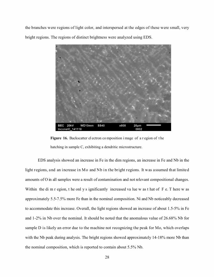
the branches were regions of light color, and interspersed at the edges of these were small, very
bright regions. The regions of distinct brightness were analyzed using EDS.
Figure 16. Backscatter el ectron co mposition i mage of a r egion of t he
hatching in sample C, exhibiting a dendritic microstructure.
EDS analysis showed an increase in Fe in the dim regions, an increase in Fe and Nb in the
light regions, and an increase in Mo and Nb in the bright regions. It was assumed that limited
amounts of O in all samples were a result of contamination and not relevant compositional changes.
Within the di m r egion, t he onl y s ignificantly increased va lue w as t hat of F e. T here w as
approximately 5.5-7.5% more Fe than in the nominal composition. Ni and Nb noticeably decreased
to accommodate this increase. Overall, the light regions showed an increase of about 1.5-5% in Fe
and 1-2% in Nb over the nominal. It should be noted that the anomalous value of 26.68% Nb for
sample D is likely an error due to the machine not recognizing the peak for Mo, which overlaps
with the Nb peak during analysis. The bright regions showed approximately 14-18% more Nb than
the nominal composition, which is reported to contain about 5.5% Nb.
28

Table 3. Summary of EDS compositional analysis, separated to show dim,
light, and bright regions in the compositional backscatter image on the face
of each sample.
Dim Sample O Al Ti Cr Fe Ni Nb Mo
A 0.93 0.50 0.73 19.54 18.64 52.48 3.45 3.73 B 0.92 0.53 0.93 20.38 20.07 51.81 2.59 2.77 C 1.83 0.64 0.55 19.91 20.28 51.81 2.13 2.84 D 2.05 0.00 0.88 21.50 20.78 54.78 0.00 0.00
Nominal 0 0.8 1.15 21 13.17 55 5.5 3.3
Light Sample O Al Ti Cr Fe Ni Nb Mo
A 1.50 0.28 1.40 17.87 17.55 51.22 6.82 3.36 B 1.01 0.58 1.14 18.68 16.91 50.19 7.64 3.85 C 1.23 0.47 1.01 19.17 18.22 49.97 6.45 3.49 D 0.00 0.00 2.11 15.51 14.65 41.05 26.68 0.00
Nominal 0 0.8 1.15 21 13.17 55 5.5 3.3
Bright Sample O Al Ti Cr Fe Ni Nb Mo
A 0.27 0.35 1.40 14.26 13.50 45.32 19.60 5.31 B 1.99 0.32 1.58 14.39 13.65 41.21 21.33 5.53 C 1.65 0.25 1.70 14.48 13.09 42.52 22.92 3.39 D 0.00 0.00 1.06 16.27 14.55 44.16 23.97 0.00
Nominal 0 0.8 1.15 21 13.17 55 5.5 3.3
2.2.2 Discussion of elemental distribution
Through the use of BEC imaging, the hatching and contour could be distinguished. Therefore, a
distinct segregation of elements must be present to create the contrast necessary for BEC images.
For the interference between the hatching and contour, Figure 15 shows a certain macro-contrast:
overall it shows regions of darkness and highlights, which together contribute to the distinction of
the two m ajor a reas. W hen t he l arge a reas are examined m ore cl osely however (Figure 16), a
29

micro-contrast within the macro-contrast can be seen. This micro-contrast defines the dendritic
microstructure which is expected from LENS, as a rapid solidification process.
Since e lemental a nalysis w as done on hi ghly m agnified r egions only, a nd t he m icro-
contrast affects the macro-contrast, the results from the micro-contrast analysis will be presented
first and then extended to explain the macro-contrast.
2.2.2.1 Micro-contrast analysis
The dendrites in the microstructure had a dim core, which contained more Fe and less Nb
and Mo than the nominal composition. Around this core was a light region, which had decreased
Fe and Nb. Within this light region were bright spots that were rich in Nb and Mo. This distribution
of elements suggests that the non-equilibrium rapid solidification that occurs during the LENS
process carried the heavier elements of Nb and Mo with the solid-liquid interface. Therefore, when
the final liquid cooled, it was saturated with Nb and Mo. These regions are likely precursors to the
γ″ phase, which consists of Ni3Nb, and is the strengthening phase in IN718. When the γ″ phase
forms, it creates the regions that are bright and are significantly richer in Nb. Though the γ″ phase
is nano-sized, a conglomeration of particles could still appear as the bright region seen in BEC
imaging. This explanation is supported by the work of Tian et al38.
2.2.2.2 Macro-contrast analysis
The results from analyzing the micro-contrast (or micro-segregation) can be used to also
examine the macro-contrast (or macro-segregation). Each of the hatching lines is outlined by a thin
line of light material. Based on the above analysis, it can be concluded that this area has an increase
in Nb and Mo. Therefore, as the melt pool as a whole cooled, more Mo and Nb were swept to the
edges and solidified there. When the next line was created, it re-melted one side of the previous
30

line a nd re-distributed t he e lements, pus hing t hem t o t he edges of i ts own m elt pool . T his
anisotropic compositional distribution continued throughout each layer of hatching.
2.3 GRAIN SIZE AND DISTRIBUTION
EBSD was used to determine grain size and distribution. The scanned area on the faces spanned
part of the hatching and part of the contour to detect any differences in grains between the two.
The scanned area on the cross-section spanned part of the substrate and the bottom layers of the
sample.
31
2.3.1 EBSD of sample faces
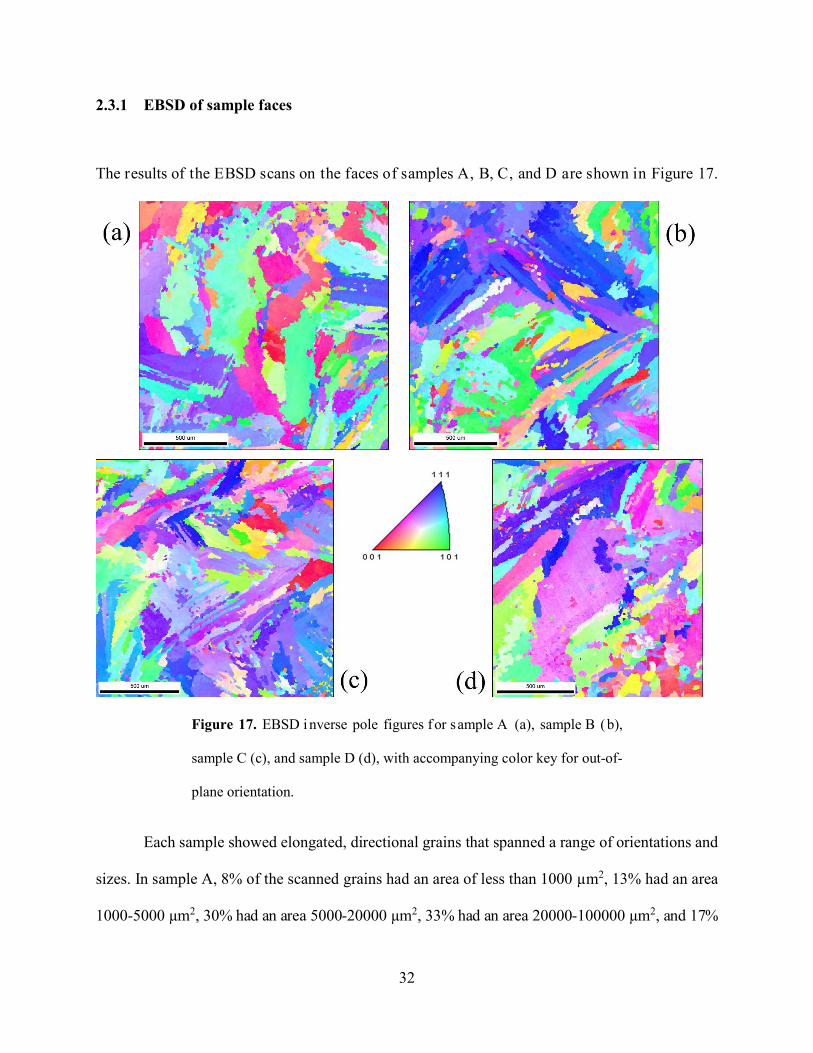
The results of the EBSD scans on the faces of samples A, B, C, and D are shown in Figure 17.
Figure 17. EBSD inverse pole figures for sample A (a), sample B (b),
sample C (c), and sample D (d), with accompanying color key for out-of-
plane orientation.
Each sample showed elongated, directional grains that spanned a range of orientations and
sizes. In sample A, 8% of the scanned grains had an area of less than 1000 µm2, 13% had an area
1000-5000 µm2, 30% had an area 5000-20000 µm2, 33% had an area 20000-100000 µm2, and 17%
32

had an area greater than 100000 µm2. With the same categories for grain sizes, the distribution for
sample B was 10%, 15%, 21%, 41%, and 13%; sample C was 18%, 13%, 16%, 26%, and 28%;
sample D was 7%, 17%, 18%, 20%, and 31% (Figure 18).
Figure 18. Grain size distribution based on EBSD data.
2.3.2 EBSD of sample cross-section
EBSD scans of the cross-section spanned much of the sample in an area where the contour and
hatching i nteract. Figure 19 shows t he r esult of t he s cans, w ith a s chematic in dicating th e
approximate area they were taken from.
33

Figure 19. EBSD image of sample 1a, from the substrate into the sample.
The top part of the scan had small, mostly equiaxed grains, with no preferred orientations.
Moving into the sample, the microstructure was still fairly fine-grained and the grains began to
34
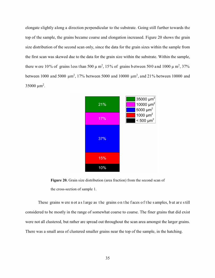
elongate slightly along a direction perpendicular to the substrate. Going still further towards the
top of the sample, the grains became coarse and elongation increased. Figure 20 shows the grain
size distribution of the second scan only, since the data for the grain sizes within the sample from
the first scan was skewed due to the data for the grain size within the substrate. Within the sample,
there were 10% of grains less than 500 µ m2, 15% of grains between 500 and 1000 µ m2, 37%
between 1000 and 5000 µm2, 17% between 5000 and 10000 µm2, and 21% between 10000 and
35000 µm2.
Figure 20. Grain size distribution (area fraction) from the second scan of
the cross-section of sample 1.
These grains w ere n ot a s l arge as t he grains o n t he f aces o f t he s amples, b ut ar e s till
considered to be mostly in the range of somewhat coarse to coarse. The finer grains that did exist
were not all clustered, but rather are spread out throughout the scan area amongst the larger grains.
There was a small area of clustered smaller grains near the top of the sample, in the hatching.
35
2.3.3 Discussion of EBSD on sample faces
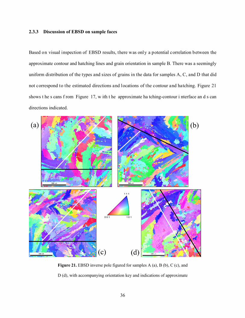
Based on visual inspection of EBSD results, there was only a potential correlation between the
approximate contour and hatching lines and grain orientation in sample B. There was a seemingly
uniform distribution of the types and sizes of grains in the data for samples A, C, and D that did
not correspond to the estimated directions and locations of the contour and hatching. Figure 21
shows t he s cans f rom Figure 17, w ith t he approximate ha tching-contour i nterface an d s can
directions indicated.
Figure 21. EBSD inverse pole figured for samples A (a), B (b), C (c), and
D (d), with accompanying orientation key and indications of approximate
36

location of h atching/contour i nterface ( black l ine) a nd s can d irection
(white line).
The EBSD micrograph of sample B shows a possible distinction between hatching lines
and the contour through orientation. The contour and a possible hatching line tend toward [111],
while the next distinct hatching line tends toward [101]. The grains appear to have aligned parallel
to the laser scan direction; however, this is not corroborated by any of the other samples. In all of
the s amples, t here was some consistency in grain or ientation across t he boundary b etween the
contour and hatching. This indicates that because of re-melting, the grains in the material that were
melted last grew in the same orientation as the already-solidified material.
Based on the area fractions of the different grain sizes, the microstructure of the faces was
primarily coarse-grained, with some finer grains distributed throughout the scan area. This means
that t he combination of processing pa rameters caused the growth of t he grains t o prevail ove r
nucleation. Because heat could not be lost to the rest of the sample and to the substrate fast enough
to give a high enough cooling rate for a nucleation-prevalent microstructure, the grains were given
ample time f or growth d uring t he s olidification pe riod. The de velopment of an el ongated
microstructure w as encouraged by t he p resence o f nucleation s ites f rom pr eviously-melted
material around the melt pool.
The discovery of coarse grains is contrary to some literature on LENS printing reporting a
fine microstructure as a result of rapid cooling13. However, Tian et al reported large, elongated
grains c reated b y LENS-printing of IN71838. It is e xpected th at th is discrepancy is du e t o
manufacturing differences that led to differences in thermal history. Since the machine that was
used in th is s tudy is o ne o f th e f irst o f its k ind (a s mall-scale LENS machine f or r esearch
laboratories) the s mall chamber experiences f ast, i ntense h eating, w hich would l essen t he
37

microstructural rapid cooling effects. Industrial machines have larger chambers which take longer
to heat up to the same temperatures. In addition, a discrepancy between the printing parameters
used in this experiment (e.g. laser power, scan speed, layer height, etc.) and those used in other
experiments could have caused enough of a difference to preclude the fine-grained microstructure.
2.3.4 Discussion of EBSD of cross-section
The c ross-section of t he LENS-printed s ample s howed m ostly large, elongated grains. T his i s
consistent w ith th at o f direct ma nufacturing p rocesses th at p artially re-melt p revious la yers39.
Large columnar grains are grown in LENS printing because the extension of the melt pool into the
layer below creates a nucleus for the cooling liquid on the existing layer. The already-solidified
grain’s or ientation therefore extends i nto t he ne w l ayer39. The E BSD scans support t his, s ince
many grains are large enough to extend through several layers. These grains experience columnar
growth because there is a positive temperature gradient from the solidified material into the melt
pool40. This columnar microstructure may be beneficial for turbine applications.
The distribution of the smaller grains amongst the columnar grains can be explained by the
overbuild of the contour. Both scans were taken from an area that was at the interface between the
contour and the hatching, where there was a bend in the layers because the hatching overlapped
the c ontour. T here are f ine g rains s cattered amongst th e columnar grains a ll w ithin this ar ea,
especially towards the top, where the overbuild was greatest. The overbuild is a bend in the layer,
which allows for several points of contact with the already-solidified material. This would hinder
solely columnar growth and increase nucleation sites, increasing the potential for growth of smaller
grains (Figure 22).
38
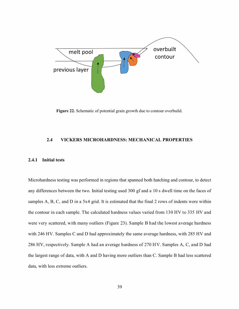
Figure 22. Schematic of potential grain growth due to contour overbuild.
2.4 VICKERS MICROHARDNESS: MECHANICAL PROPERTIES
2.4.1 Initial tests
Microhardness testing was performed in regions that spanned both hatching and contour, to detect
any differences between the two. Initial testing used 300 gf and a 10 s dwell time on the faces of
samples A, B, C, and D in a 5x4 grid. It is estimated that the final 2 rows of indents were within
the contour in each sample. The calculated hardness values varied from 130 HV to 335 HV and
were very scattered, with many outliers (Figure 23). Sample B had the lowest average hardness
with 246 HV. Samples C and D had approximately the same average hardness, with 285 HV and
286 HV, respectively. Sample A had an average hardness of 270 HV. Samples A, C, and D had
the largest range of data, with A and D having more outliers than C. Sample B had less scattered
data, with less extreme outliers.
39

Figure 23. Vickers hardness va lues for 5x4 gr id spanning hatching and
contour. Test load of 300 gf and dwell time of 10 s were used. (a) sample
A, (b) sample B, (c) sample C, (d) sample D
In order to collect more data and to attempt to decrease the standard deviation, another set
of 5x4 grids were made, with an increased force of 500 gf. It is estimated that the final 2-3 rows
of indents were within the contour out of the four in each sample. Overall, the standard deviation
decreased and there were less extreme outliers (Figure 24). Sample B had an average hardness of
225 HV, and samples C and D had only slightly higher average hardness values of 232 HV and
233 HV. As in the first test, samples C and D had almost the same average hardness, but in the
40
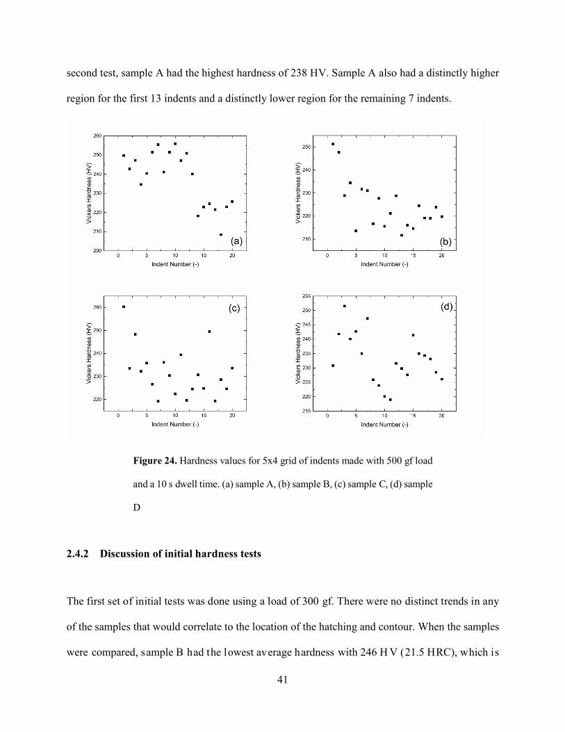
second test, sample A had the highest hardness of 238 HV. Sample A also had a distinctly higher
region for the first 13 indents and a distinctly lower region for the remaining 7 indents.
Figure 24. Hardness values for 5x4 grid of indents made with 500 gf load
and a 10 s dwell time. (a) sample A, (b) sample B, (c) sample C, (d) sample
D
2.4.2 Discussion of initial hardness tests
The first set of initial tests was done using a load of 300 gf. There were no distinct trends in any
of the samples that would correlate to the location of the hatching and contour. When the samples
were compared, sample B had the lowest average hardness with 246 H V (21.5 HRC), which is
41

closest to the reported values of hardness for a room-temperature hot-rolled round41. Samples C
and D had the highest hardness of 285 HV and 286 HV (29.8 HRC and 30.0 HRC). These values
are still lower than many of the reported hardness values for IN718, and they are in the range of
values for a room-temperature hot-rolled bar41. Since a 300 gf load produced very scattered data,
the load was increased in an attempt to increase precision and accuracy.
A 500 gf load increased the precision slightly, though the data was still somewhat scattered.
Sample B still had the lowest hardness, sample A was the hardest based on this set of tests, and
samples C and D still remained at almost the same hardness as each other. These consistent patterns
and tendencies imply that there may be a difference in the hardness of the top layers of the samples:
the printing parameters of sample B may have caused it to have a lower hardness, and the printing
parameters o f s amples C and D may be s imilar enough to each other to have no effect on t he
hardness of the final samples. These hypotheses were evaluated through further testing.
In t he s econd t est, there was again no di fference between the hatching and contour for
samples B, C, and D; however, sample A showed a distinct difference in hardness between the
hatching and the contour (Figure 25). Since the exposed surface was in an interlayer region, the
pore density was lower in the hatching than in the contour, as discussed previously. This lower
pore density left more material intact, and may have resulted in a higher average hardness. In the
contour of sample A, where there were an increased number of densely-packed pores, the average
hardness was lower by approximately 10%.
42

Figure 25. Distinction of the hatching and contour hardness values for the
second set of hardness tests, with 500 gf load and 10 s dwell time.
2.4.3 Subsequent hardness testing
Since data from the initial tests was insufficient to confirm any hypotheses about differences in
hardness between or within samples, subsequent testing was performed. First, a 5x6 grid of indents
was made on each sample in a manner that spanned both the hatching and contour, with the final
2-3 rows in the contour. Then, hardness maps of the top and center slices of sample A were created.
These maps sampled a quarter of the sample face, in order to infer the behavior of the remaining
symmetrical ¾ of the samples (Figure 9Error! Reference source not found.).
2.4.3.1 Average hardness by row
Plotted averages of each row for each sample are shown in Figure 26. The first rows are in
the ha tching, and the hi gher number rows progressed into t he contour. Sample A h ad a s light
increasing trend with increasing row number, from 221 H V to 241 HV. Sample B decreased in
43

hardness from 237 H V in row 1 t o 218 H V in row 5, a nd increased again to 231 H V in row 6.
Sample C ha d a s imilar t rend, de creasing f rom 238 H V i n r ow 1 t o 22 6 H V i n r ow 5, t hen
increasing to 232 HV in row 6. Sample D had consistently higher hardness values than the other
samples, but did not have a distinct trend. Sample D started at 254 HV for row 1, decreased to 244
HV by row 3, increased to 252 HV in row 4, decreased to 240 HV in row 5, and increased again
in row 6 to 249 HV.
Figure 26. Average hardness per row for initial testing of samples A, B,
C, and D.
An average of overall hardness for each sample is shown in Table 4. Sample D had a higher
hardness value than samples A, B, and C with 247 HV. Sample B had the lowest hardness of 228
HV. Samples A and C both had an average of 232 HV.
44

Table 4. Average initial Vickers microhardness values for samples A, B,
C, and D.
Sample Hardness (HV) A 232 B 228 C 232 D 247
2.4.4 Discussion of subsequent hardness testing
Though it appeared from the initial tests that there may be a difference in the hardness values in
the contour and the hatching, there is no evidence to support this in the subsequent testing. There
was no sharp decrease such as that seen in sample A from the initial tests (Figure 25), nor was
there any consistent trend between the samples.
Consistent with the initial tests, sample B had a lower hardness; though by much more of
an insignificant margin. Only 4 HV difference from a 5x6 grid of indents is not enough to conclude
that the bulk hardness is lower than the other samples. Instead of samples C and D having almost
the same hardness, samples A and C had similar hardness averages. As with the first set of tests,
sample D had the highest hardness.
2.4.5 Hardness mapping
To improve the hardness measurements and to better understand the hardness distribution and local
effects, t he h ardness was m apped on s lices, f aces, and c ross-sections on sample A in or der t o
determine if there was a distinct hardness distribution pattern.
45

2.4.5.1 Hardness mapping on slices
Sample A was cut into three slices: bottom, center, and top. These slices represented three
different areas of thermal history.
The center slice was in the fourth or fifth layer, and had an average hardness of 263 HV.
There was a distinct pattern to the hardness distribution: harder within the hatching, and less hard
within the contour (Figure 27). The difference in the average hardness of the contour region and
hatching region was approximately 20 HV. The highest hardness of 368 HV occurred at the top
right corner o f t he t esting area. The bottom le ft corner, c orresponding with t he c orner of t he
sample, had the lowest hardness values, with the lowest being 213 HV.
46
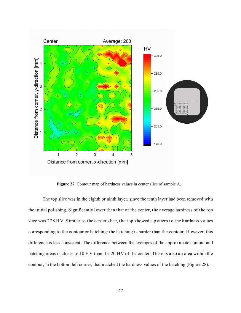
Figure 27. Contour map of hardness values in center slice of sample A.
The top slice was in the eighth or ninth layer, since the tenth layer had been removed with
the initial polishing. Significantly lower than that of the center, the average hardness of the top
slice was 228 HV. S imilar to the cen ter s lice, the top showed a p attern t o the hardness values
corresponding to the contour or hatching: the hatching is harder than the contour. However, this
difference is less consistent. The difference between the averages of the approximate contour and
hatching areas is closer to 10 HV than the 20 HV of the center. There is also an area within the
contour, in the bottom left corner, that matched the hardness values of the hatching (Figure 28).
47

Figure 28. Contour map of hardness values in the top slice of sample A.
2.4.5.2 Hardness mapping on cross-section
Sample 1 was cut in half perpendicular to the substrate, and the cross-section was examined
by creating a map of hardness values from the contour of the left side into the hatching (Figure
10). The data is shown in a contour map in Figure 29. The average of the hardness within the
sample w as 282 H V. T he a verage ha rdness w ithin t he c ontour was 274 H V, and t he average
hardness within the hatching was slightly higher, at 290 HV. Overall, the contour was consistently
48

lower in hardness than the hatching, and the top overbuilt region of the contour had the lowest
average hardness of approximately 259 HV.
Figure 29. Hardness mapping for cross-section of sample 1.
2.4.6 Discussion of hardness mapping
Both the top and center slices indicated that there was a d ifference between the hardness of the
contour and that of the hatching. This supports the results from the initial tests (section 2.4.2),
though not t he s ubsequent t ests (section 2.4.4). It i s pos sible t hat t he subsequent t ests w ere
performed in an area which happened to show less difference in hardness between the two regions,
49

such as the bottom left corner and the hatching in Figure 28 (the top slice). The mapping presents
more reliable results since the testing area was not arbitrarily selected. As has been discussed, the
properties of a material a re known to be anisotropic t hroughout a LENS-printed pa rt, and this
anisotropy is apparent here, both through the inconsistency of the small-grid hardness tests and
through pattern formation in the results of the hardness mapping.
The cau se o f t he d ifference i n h ardness co uld b e a r esult o f s everal f actors: t he p ores
discussed i n s ection 2.4.2, the f ormation of di fferent-sized grains w ithin t he c ontour, or the
existence of different phases. It is not likely to be only an effect of the pores, since the samples
used for mapping were not confirmed to be both polished to an interlayer surface; in addition, the
dark f ield o ptical m icroscopy of t he cross-section di d not s how a c lear di fference i n po re
distribution between the hatching and the contour. The formation of different-sized grains within
the contour is possible due to different thermal history, but the EBSD results in section 2.3 show
no indication that this is a s ignificant consideration either for the sample face or for the cross-
section.
The existence of a different phase distribution is possible. The matrix of IN718 is γ-phase,
and the primary strengthening phase is γ″. Though γ″ is nano-sized, the particles can conglomerate
and make an area rich in γ″. This effect, and the particles’ presence in Nb- and Mo-rich areas was
explored by Tian et al38. In section 2.2.2.2, the macro-segregation in the face of the samples was
discussed, and it was concluded that solidification caused Nb and Mo to be swept to the edges of
dendrites as well as the edge of melt pools. With an increased number of overlapping melt pools
in the contour, these elements would get redistributed more frequently and in a more scattered
manner, not allowing for the formation of a significant amount of γ″ in any one region. In the
hatching however, Nb and Mo are swept systematically to the parallel edges of the melt pool as
50

the laser scans back and forth. This alignment of melt pool edges could allow for the formation of
more conglomerated γ″ particles, which would result in a higher average hardness value in the
hatching.
51
3.0 FUTURE WORK
When beginning this work, the ASM Handbook was consulted for grinding and polishing methods,
and t he information f or ni ckel was u sed42. It was di scovered a fter ha ving be gun t he s ample
preparation that it produces better results to use the information for heat-resistant alloys instead.
For consistency, the method was not changed for the duration of this study; however, future work
will involve using surface preparation for heat-resistant alloys and comparing the results to those
presented i n t his s tudy t o obt ain m ore r esults a nd isolate a ny effects r esulting from th e
metallographic preparation methods used. With the change of the preparation method, more EBSD
results w ill be obt ained in or der t o f urther e xamine t he t exture a nd grain s ize t hroughout t he
samples, both parallel and perpendicular to the substrate. XRD may also be used to characterize
phase distribution. Once the characterization is complete and linked to potential processing factors,
the printing process will be systematically changed in order to reverse engineer the microstructure
of the LENS-printed material.
Porosity will be analyzed further by doing additional powder and sample characterization.
Powders will be mounted in epoxy and ground to expose the center of some particles, which will
be e xamined f or i nternal por osity a nd t rapped a ir. Samples w ill b e e xamined u sing c omputer
tomography to more accurately analyze pore shape, size, and distribution.
The m ethods a nd m aterials w ill a lso be e xpanded upon. O nce t he c urrent m ethod a nd
material are understood, the project will be expanded to involve powder bed binder jet printing
and IN625. Effects of variables such as powder size distribution, sintering time and temperature,
and heat treatment methods will be evaluated. Effects of powder production method on both the
powder bed binder jet printing and LENS printing will also be evaluated.
52

4.0 CONCLUSION
This study has explored the microstructural and mechanical properties of a nickel-based superalloy
that has been additively manufactured. The material and process in focus were IN718 and Laser
Engineered N et S haping, r espectively. R esults f rom opt ical m icroscopy, s canning e lectron
microscopy, energy-dispersive X-ray spectrometry, electron backscatter diffraction, and Vickers
microhardness were analyzed.
1. The c omparison be tween t he pol ished a nd r e-polished s amples i n c onjunction w ith c ross-
sectional images showed that the pore distribution is likely associated with melt pool edges. The
placement and interaction of these melt pool edges caused the intralayer hatching to be traced out
by the pores, and the interlayer hatching as well as the contour to have densely-packed, randomly-
distributed pores.
2. Elemental an alysis s howed t hat t here was m icro-segregation as w ell as m acro-segregation
present in the samples. The micro-segregation was caused by dendritic solidification, and resulted
in a Fe-rich core, a slightly Nb-rich interdendritic region, and some very Nb-rich spots. Macro-
segregation resulted in a Mo- and Nb-rich region at the edge of the last-melted area, which defined
the boundary between the hatching and contour as well as between scan lines.
3. Grain size and distribution examination of the face revealed coarse, elongated grains that did
not va ry s ignificantly be tween ha tching and contour. Therefore, grains o f a certain or ientation
continue from one region to another due to re-melting. Grain size and distribution examination of
53

the cr oss-section al so s howed co arse, el ongated grains t hat d id n ot v ary significantly b etween
hatching and contour. These elongated, columnar grains indicate that the solidified material in the
previous layer serves as a nucleation site for the melt pool. Also, the bend in solidified material
due to the overbuild of the contour may allow for more nucleation sites, resulting in more, smaller
grains at this bend.
4. Initial and subsequent hardness testing with small grids of indents revealed no recognizable,
consistent t rend i n ha rdness da ta, either i n i ndividual s amples or be tween s amples. Hardness
mapping revealed a difference in the average hardness of the contour and the hatching. Locally,
there was sometimes a great deal of variation, which highlights the shortcomings of small grid
tests of arbitrary areas. The two slices that were tested on the face (top and center) both showed
the hatching/contour variation, which may be a result of increased γ″ formation instigated by the
macro-segregation of Nb and Mo.
54

APPENDIX A
ABBREVIATIONS
AM additive manufacturing
BCT body-centered tetragonal
BEC backscatter electron composition (image)
CAD computer-aided design
DOM digital optical microscope
EBSD electron backscatter diffraction
EDS energy-dispersive X-ray spectroscopy
FCC face-centered cubic
HAZ heat-affected zone
IN718 Inconel alloy 718
LENS Laser Engineered Net Shaping
PM powder metallurgy
PREP plasma rotating electrode process
SEM scanning electron microscope
55

BIBLIOGRAPHY
1. Mellor, S., Hao, L. & Zhang, D. Additive manufacturing: A framework for implementation.
Int. J. Prod. Econ. 149, 194–201 (2014).
2. Holmström, J., Partanen, J., Tuomi, J. & Walter, M. Rapid manufacturing in the spare parts
supply chain: Alternative approaches to capacity deployment. J. Manuf. Technol. Manag.
21, 687–697 (2010).
3. Frazier, W. E. Metal additive manufacturing: A review. J. Mater. Eng. Perform. 23, 1917–
1928 (2014).
4. Gebhardt, A. Glossary: Terms and Abbreviations. Underst. Addit. Manuf. 151–164 (2011).
doi:http://dx.doi.org/10.3139/9783446431621.bm
5. ASTM International. F 2792-12a - Standard T erminology for A dditive M anufacturing
Technologies. 10–12 (2013). doi:10.1520/F2792-12A.2
6. Gibson, I., Rosen, D . W. & S tucker, B . Additive Manufacturing Technologies. Springer
Science + Business Media, LLC (2010). doi:10.1007/978-1-4419-1120-9
7. Moroni, G., Syam, W. P. & Petr, S. Towards early estimation of part accuracy in additive
manufacturing. 21, 300–305 (2014).
8. Gebhardt, A. in Understanding Additive Manufacturing 1–29 (Hanser Publishers, 2012).
9. Dudziak, A. et al. Accuracy of parts manufactured by rapid prototyping technology. (2010).
10. Gebhardt, A. in Understanding Additive Manufacturing 31–63 (Hanser Publishers, 2011).
doi:http://dx.doi.org/10.3139/9783446431621.002
11. Manvatkar, V. D., Gokhale, a. a., Jagan Reddy, G., Venkataramana, a. & De, a. Estimation
of melt pool dimensions, thermal cycle, and hardness distribution in the laser-engineered
56

net s haping pr ocess of austenitic s tainless s teel. Metall. Mater. Trans. A Phys. Metall.
Mater. Sci. 42, 4080–4087 (2011).
12. Palčič, I., Balažic, M., Milfelner, M. & Buchmeister, B. Potential of Laser Engineered Net
Shaping (LENS) Technology. Mater. Manuf. Process. 24, 750–753 (2009).
13. Grylls, R. Laser Engineered Net Shapes.pdf. 45–46 (2003).
14. Keicher, D . M . & S mugeresky, J . E . T he l aser f orming of m etallic c omponents us ing
particulate materials. Jom 49, 51–54 (1997).
15. Liu, D. et al. Laser Engineered Net Shape (LENS) Technology for the Repair of Ni-Base
Superalloy Turbine Components. Metall. Mater. Trans. A 45, 4454–4469 (2014).
16. Cooper, K. P. Building components by laser-additive processing. Jom 53, 29–29 (2001).
17. Liu, W. & Dupont, J. N. In-situ reactive processing of nickel aluminides by laser-engineered
net shaping. Metall. Mater. Trans. A 34, 2633–2641 (2003).
18. Tobar, M ., A mado, J ., Lamas, J . & Y áñez, a. E ffect of P rocessing P arameters i n
Manufacturing of 3D parts Through Laser Direct Metal Deposition. 4–7
19. Donachie, M . J. & D onachie, S . J . Superalloys: a technical guide. ( ASM International,
2002).
20. Reed, R. C. The superalloys: fundamentals and applications. (Cambridge University Press,
2006).
21. Smith, G. D. & Patel, S. J. The Role of Niobium in Wrought Precipitation-Hardened Nickel-
Base A lloys. Superalloys 718, 625, 706 Var. Deriv. 135–154 ( 2005).
doi:10.7449/2005/Superalloys_2005_135_154
57
22. Kulawik, K., Buffat, P. a., Kruk, a., Wusatowska-Sarnek, a. M. & Czyrska-Filemonowicz,
a. Imaging and characterization of γ′ and γ″ nanoparticles in Inconel 718 by EDX elemental
mapping and FIB–SEM tomography. Mater. Charact. 100, 74–80 (2015).
23. Wang, L., Felicelli, S., Gooroochurn, Y., Wang, P. T. & Horstemeyer, M. F. Optimization
of the LENS?? process for steady molten pool size. Mater. Sci. Eng. A 474, 148–156 (2008).
24. Zhang, Y., Li, Z., Nie, P. & Wu, Y. Effect of cooling rate on the microstructure of laser-
remelted INCONEL 718 c oating. Metall. Mater. Trans. A Phys. Metall. Mater. Sci. 44,
5513–5521 (2013).
25. Zhao, X., Chen, J., Lin, X. & Huang, W. Study on microstructure and mechanical properties
of laser rapid forming Inconel 718. Mater. Sci. Eng. A 478, 119–124 (2008).
26. Porter, D. A., Easterling, K. E. & Sherif, Y. Phase Transformations in Metals and Alloys.
Annual Review of Materials Science 3, (2009).
27. Hofmeister, W. & Griffith, M. Solidification in direct metal deposition by LENS processing.
JOM 53, 30–34 (2001).
28. Yin, H. & Felicelli, S . D. Dendrite growth s imulation during solidification in the LENS
process. Acta Mater. 58, 1455–1465 (2010).
29. Qi, H., Azer, M. & Ritter, A. Studies of Standard Heat Treatment Effects on Microstructure
and M echanical P roperties o f Laser N et S hape M anufactured INCONEL 7 18. Metall.
Mater. Trans. A 40, 2410–2422 (2009).
30. Zheng, B ., Zhou, Y ., S mugeresky, J . E ., S choenung, J . M . & Lavernia, E . J . T hermal
behavior a nd m icrostructure e volution dur ing l aser de position w ith l aser-engineered n et
shaping: Part II. Experimental investigation and discussion. Metall. Mater. Trans. A Phys.
Metall. Mater. Sci. 39, 2237–2245 (2008).
58

31. Peter J . G oodhew, F . J . H umphreys, R . B. Electron microscopy and analysis. Electron
Microscopy and analysis (2001).
32. Garratt-Reed, a J . & Bell, D . C . E nergy-Dispersive X -Ray Analysis i n t he E lectron
Microscope. Microscopy 49, 1–13 (2003).
33. Stojakovic, D. Electron backscatter diffraction in materials characterization. Process. Appl.
Ceram. 6, 1–13 (2012).
34. Cullity, B. D. & Stock, S. R. Elements of x-ray diffraction. (Prentice Hall, 2001).
35. Astm. ASTM E 407 Standard Practice for Microetching Metals and Alloys 1. 1–21 (2005).
doi:10.1520/E0407-07.2
36. Hardness testing: principles and applications. (ASM International, 2011).
37. Dieter, G . & B acon, D . Mechanical Metallurgy. McGrawHill Shoppenhangers Road
Maidenhead Berkshire SL2 2QL UK 1988 (1988).
38. Tian, Y. et al. Rationalization of Microstructure Heterogeneity in INCONEL 718 B uilds
Made by the Direct Laser Additive Manufacturing Process. (2014). doi :10.1007/s11661-
014-2370-6
39. Vilaro, T., Colin, C. & Bartout, J. D. As-fabricated and heat-treated microstructures of the
Ti-6Al-4V alloy processed by selective laser melting. Metall. Mater. Trans. A Phys. Metall.
Mater. Sci. 42, 3190–3199 (2011).
40. Kurz, W., Bezençon, C. & Gäumann, M. Columnar to equiaxed transition in solidification
processing. Sci. Technol. Adv. Mater. 2, 185–191 (2001).
41. INCONEL alloy 718. 1–27 (2007).
42. ASM-Standard. Metallography and Microstructures of Nonferrous Alloys. ASM Handb. 9,
711–751 (2004).
59

60
Recommended