Copyrighted (Textbook) Fei Hu and Xiaojun Cao, Wireless Sensor Networks: Principles and Practice, CRC Press Page 1
Chapter 2: Hardware ‐ Sensor Mote Architecture and Design
In this chapter, we will go through the hardware design details of sensor nodes. A WSN
sensor node (also called a mote) consists of analog sensors, microcontroller, memory, RF (Radio
Frequency) communication unit, battery, and other components. We will use [Lester03] as the
main reference since it has pioneering sensor mote design.
This chapter also covers some physical layer concepts in WSNs (such as modulation,
wireless signal transmissions, etc.). The next a few chapters will cover higher layers details (such
as MAC layer, routing layer, transport layer, etc.).
In this chapter, we will first discuss each component of the sensor mote. Later on we will
put everything together into an intelligent sensor mote.
2.1 Components of a Sensor Mote [Lester03]
In the following we will explain the hardware components of a sensor mote. Each of the
components should be designed from both operation performance and energy efficiency
viewpoint.
Copyrighted (Textbook) Fei Hu and Xiaojun Cao, Wireless Sensor Networks: Principles and Practice, CRC Press Page 2
2.1.1 Sensors
Thousands of different analog/digital sensors have been invented and ready to be attached
to a wireless sensing platform to form a WSN node (also called “mote”). Recent advances in
MEMS and carbon nano-tubes technology have enabled many different types of sensors. Some
examples are chemical sensors and digital nose. Table 2.1 lists some common micro-sensors and
their main features [Lester03].
Place Table 2.1 here.
Table 2.1 Power consumption and capabilities of commonly available sensors [Lester03]
Analog and digital sensors have the following different characteristics:
(1) Analog sensors generate raw analog voltage values based on the physical phenomena
that they are measuring. They produce a continual waveform, which needs to be digitized (i.e.,
forming digital signals such as 0101001 …) by special chips (such as an ADC, i.e., analog-to-
digital converter). Those digital signals can then be easily processed by CPU and DSP (Digital
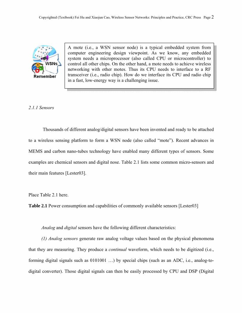
A mote (i.e., a WSN sensor node) is a typical embedded system from computer engineering design viewpoint. As we know, any embedded system needs a microprocessor (also called CPU or microcontroller) to control all other chips. On the other hand, a mote needs to achieve wireless networking with other motes. Thus its CPU needs to interface to a RF transceiver (i.e., radio chip). How do we interface its CPU and radio chip in a fast, low-energy way is a challenging issue.

Copyrighted (Textbook) Fei Hu and Xiaojun Cao, Wireless Sensor Networks: Principles and Practice, CRC Press Page 3
Signal Processing) chips.
After receiving those raw analog data, a CPU must then process such analog data in order
to produce a reading in meaningful units. For example, when an accelerometer generates a raw
reading of 0.815 Volts, it must be translated into a meaningful (i.e. human-understandable)
acceleration measurement. Does the 0.815 volts correspond to an acceleration of 0.5 m/s or 1.1
m/s? Such an analog data translation procedure could be a complicated process because of
sensors’ different timing and voltage scales.
Because the output voltage generally has a DC offset among a time-varying signal, we
typically use amplifiers and filters to match the output of the sensor to the range and fidelity of
the ADC.
(2) Digital sensors actually put all of the abovementioned voltage processing hardware in
a sensor to directly provide a clean digital interface. Because they have implemented all required
compensation and linearization internally, their output is already a digital reading with an
appropriate scale.
If you purchase a commercial microcontroller (CPU) to interface the above sensors, it
typically has multiple interfaces to either analog or digital sensors.
Since sensors have limited power output, and the WSN sensors are typically designed to
be disposable, we need to carefully control how quickly a sensor can be enabled, sampled, and
disabled since those operations have huge impacts on energy consumption. For instance,
although most sensors have the capability of producing thousands of samples per second, in
practice we are only interested in a few samples per minute. Such a low duty cycle (percentage of
active time) can greatly save energy.
Although it is important to minimize the active time of a sensor (i.e., putting the sensor to

Copyrighted (Textbook) Fei Hu and Xiaojun Cao, Wireless Sensor Networks: Principles and Practice, CRC Press Page 4
sleep as long as possible), it is also important to minimize the “transition” time, that is, the
sensor should be turned on / off as quickly as it can in order to save energy. For example, if a
sensor takes 100 ms to turn on and reads a sample, assume the sample reading consumes just 1
mA at 3V, it will cost 300 µJ in total to get a sample. This is the same amount of energy as a
sensor that consumes 1000 mA of current at 3 V but takes only 100 us (i.e., 1000 times faster) to
turn on and read a sample.
In some applications, the voltage requirements may not match well with the battery
outputs. Then extra circuit may be needed. For instance, some sensors require +/- 6 V. If a
sensor just uses AA or lithium batteries, we need special voltage converters and regulators in
order to use this sensor. The power consumption and turn-on times of converters and regulators’
circuitry must be included in the total energy budget for the sensor.
2.1.2 Microprocessor
Another important component, called microcontrollers (i.e. tiny CPUs, also called
microprocessors or processors), has pins (i.e., interfaces) to integrate flash storage, RAM, ADC
converters, and digital I/O onto a single integrated circuit. Such tight integration makes them
Today, almost all analog sensors convert environmental parameters into a readable low voltage level. How to interpret those voltage levels from event detection perspective is a difficult issue. Moreover, we need to capture such a weak current and use ADC to get digital signals. During the ADC the noise from hardware and environments should be removed.

Copyrighted (Textbook) Fei Hu and Xiaojun Cao, Wireless Sensor Networks: Principles and Practice, CRC Press Page 5
ideal for use in deeply embedded systems like WSNs.
When we select a commercial microcontroller family for a WSN application, we need to
consider some of the application requirements including power consumption, voltage
requirements, cost, support for peripherals, and the number of external components required.
Some of them will be explained as follows:
Power consumption: Different microcontrollers have very different power consumption
levels. For instance, 8 or 16 bit microcontrollers have varied power consumption between 0.25 to
2.5 mA per MHz. Such a wide difference (over 10 times) between low-power and standard
microcontrollers determines the WSN system performance significantly.
Many people think that sleep can put a sensor in complete “relaxation” status and thus
power consumption is minor in sleep status. This is not true in reality. In sleep mode, the CPU
stops execution. However, it still maintains some basic memory control activities and time
synchronization in case later on it needs to timely wake-up. The electric current consumption in
sleep mode varies from 1 µA to 50 µA across CPU families. Since the CPU is expected to be idle
99.9% of the time, such a 50x µA difference can have a more significant impact on mote
performance than mA differences in peak power consumption.
As mentioned before, the energy consumption also depends on how much time the
operation of entering / exiting sleep mode takes. Such a transition time (entering sleep / wake-up
time) could take 6 µs ~ 10 ms. The wake-up delay is used to start and stabilize system clocks.
The faster a CPU can enter or leave the sleep mode, the more energy a mote can save. As a
matter of fact, by quickly wake-up, we can put a mote into sleep mode even at a very short
period of inactivity. For example, when sending out a packet, the controller can even enter the
sleep mode among “bits”. Thus we save lots of energy.
Copyrighted (Textbook) Fei Hu and Xiaojun Cao, Wireless Sensor Networks: Principles and Practice, CRC Press Page 6
Voltage requirements: CPU performance also depends on the operating voltage range.
Traditional WSN microcontrollers operate between 2.7V and 3.3 V. Recently, new generations
of low-power CPUs can even operate on 1.8 V. WSN applications need a wide voltage tolerance.
CPU speed: In a WSN, the CPU needs to execute the wireless communication protocols
and perform local data processing. Those operations do not need a high-speed CPU. That’s why
most of today’s WSN CPUs have a speed of less than 4M Hz. To select a proper CPU speed,
we need to know the amount of sensor data processing. The CPU must be able to finish the
operations within delay deadlines.
Dynamic CPU speed: Some WSN CPUs can dynamically change the operating frequency
(i.e. CPU speed). CMOS power consumption obeys the equation P=CV2F. Therefore, higher
CPU frequency brings more power consumption. But the CPU execution time is inversely
proportional to frequency. That is, higher frequency makes a program run faster, which also
saves energy. Therefore, we cannot say that the sensor energy consumption will change a lot by
increasing or reducing CPU frequency.
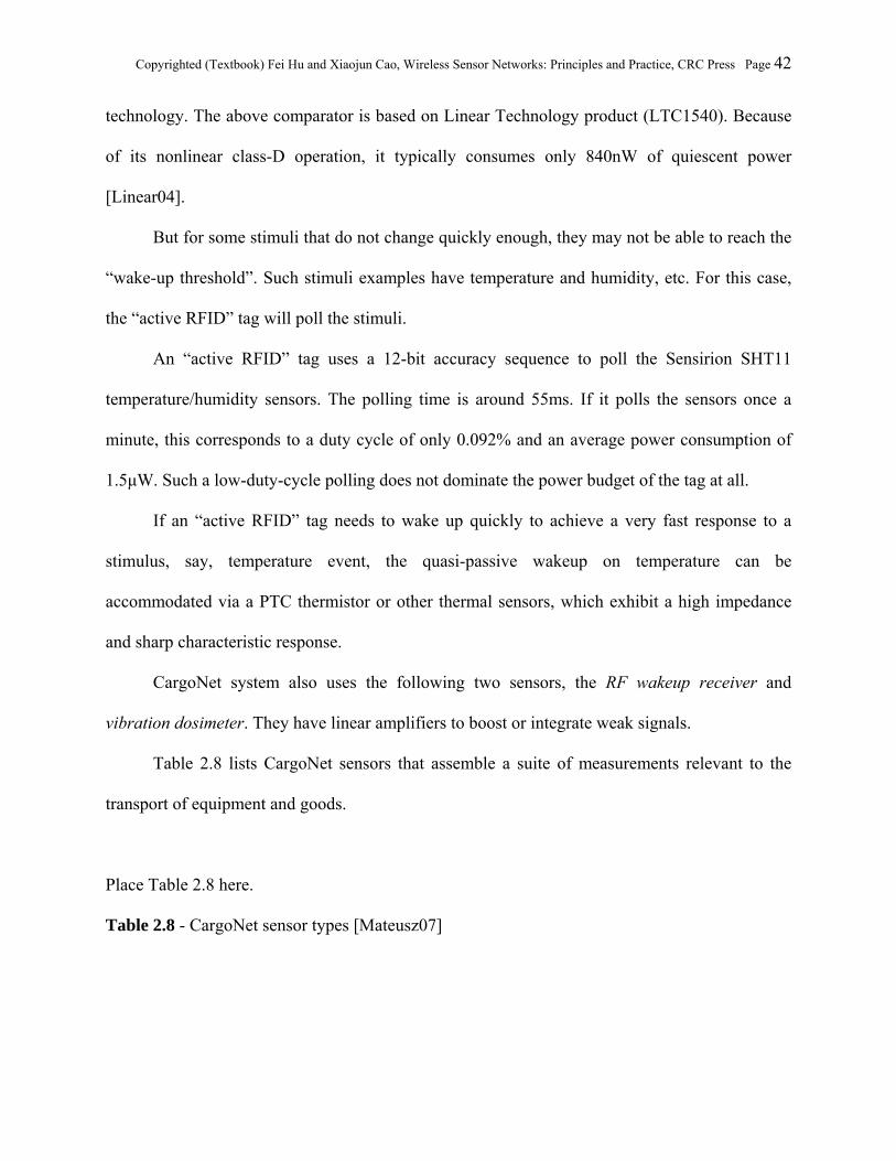
Table 2.2 lists some important features to be considered when selecting a CPU, such as
power, memory size, fast reprogrammability, A/D channels, and operating supply. It compares
some suitable CPUs in different motes on the market. Typically Atmel AT90LS8535 offers a
good performance in most WSN applications.
Place Table 2.2 here.
Table 2.2 Comparison of Microprocessors [Seth00]
Copyrighted (Textbook) Fei Hu and Xiaojun Cao, Wireless Sensor Networks: Principles and Practice, CRC Press Page 7
A CPU design example: SNAP/LE [Virantha04]
In [Virantha04] the author presents the design of a low-power microcontroller called
SNAP/LE (Sensor Network Asynchronous Processor/Low Energy), optimized for data
monitoring operations in WSNs.
SNAP/LE does not just simply select a conventional microprocessor for low-energy
optimization. Instead, it is a self-designed, brand-new microprocessor with new hardware
support for commonly-occurring operations in WSN. It aims to maximize the lifetime of a
network. SNAP/LE is event-driven with extremely low-overhead transitions between active and
idle periods.
A dominant feature of SNAP/LE is to use automatic, fine-grained power management,
which can be seen from the following fact: when a circuit does not perform a particular
operation, it won’t have any circuit switching activities. Such asynchronous circuits also remove
glitches / switching hazards in the CPU, which avoids another source of energy waste.
Another interesting feature of SNAP/LE is that its hardware directly supports sensor
event execution, which means that we don’t need an operating system (OS) such as TinyOS ! No
OS reduces static and dynamic instruction counts. It also simplifies CPU design since we don’t
need to worry about precise exceptions and virtual memory translation.
Note that the above table does not intend to list all advanced CPUs used in different embedded systems. Instead, it only lists some popular microcontrollers that may be suitable to small, low-power, low-cost motes. In some products, the microcontrollers are integrated with different memories (such as flash, ROM, etc.).

Copyrighted (Textbook) Fei Hu and Xiaojun Cao, Wireless Sensor Networks: Principles and Practice, CRC Press Page 8
Most of traditional mote CPUs adopt a commodity off-the-shelf (COTS) microcontroller
such as Berkeley motes’ Atmel Mega128L [Atmel08]. SNAP/LE doesn’t use a commercial
CPU; instead, it is a processor designed specifically for low-energy WSNs. It not only meets the
computational demands of a WSN node, but also consumes much less energy than other CPUs.
SNAP/LE aims to design a CPU with all the following features:
(1) A simple programming model: A good CPU design should allow easy programming. Its
programming model should support the following operation mode: WSN motes sleep
most of the time, periodically waking up to handle radio traffic or sensor data.
Additionally, the CPU should efficiently execute most common WSN tasks such as
scheduling internal timers or reading sensor data. SNAP/LE was designed with these
features in mind.
(2) Lower-power sleep mode: As we mentioned before, sensors remain in sleep status during
most of the time. SNAP/LE is designed in extra low power consumption while it is in
sleep status.
Good Idea
Customized VLSI vs. COTS design: It is hard to say which one is the winner. Typically, from time and complexity viewpoint, most researchers choose to use COTS since so many different companies are providing high-performance, low-cost chips to assemble a mote. However, from cost and performance viewpoint, customized VLSI design is the final solution since you could minimize chip size and achieve the best speed/energy performance. Later on, we will cover Spec [Lester03]. Like SNAP/LE, it is also a customized design.

Copyrighted (Textbook) Fei Hu and Xiaojun Cao, Wireless Sensor Networks: Principles and Practice, CRC Press Page 9
(3) Low-overhead wakeup mechanism: Since a fast transition between sleep and wake-up is
needed in order to save energy, SNAP/LE aims to achieve around 10ns of transition time,
which is much less than a typical sensor event handling time (a few ms).
(4) Low power consumption while awake: Besides keeping a low power consumption during
sleep status, SNAP/LE also minimizes the energy while in “awake” (computing) status.
SNAP/LE uses a 16-bit data path. Its instructions can be one or two 16-bit words long
(two-word instructions take two CPU clock cycles to execute).
Simultaneous execution of several instructions is supported in SNAP/LE. Its potential
concurrency can be seen from its micro-architecture in Figure 2.1. The event queue stores
outstanding events that are yet to be processed. These instruction tokens travel through the
pipeline and are transformed by the computation blocks (adders, decoders, etc.).
SNAP/LE uses data-driven switching activity to reduce the total switching capacity of
the processor. It thus saves energy. The use of asynchronous (i.e. data-driven) circuits further
enables energy savings. (To achieve equivalent savings in a clocked processor, the designer
would have to clock gate and every latch in the processor.)
Place Figure 2.1 here.
Figure 2.1 Microarchitecture of SNAP/LE showing major units. [Virantha04]
SNAP/LE CPU core includes an important component, i.e., the event queue. It works
with the instruction fetch unit to form a hardware implementation of a FIFO task scheduler. The
scheduler first executes the boot code. When the scheduler reaches “done” instruction, which is
Copyrighted (Textbook) Fei Hu and Xiaojun Cao, Wireless Sensor Networks: Principles and Practice, CRC Press Page 10
also the last instruction in the boot code, it will stop fetching instructions and wait for an event
token to appear at the head of the event queue.
Each event token tells what event has occurred. Event tokens are inserted into the event
queue by two hardware components: (1) the timer coprocessor when a timeout finishes; (2) the
message coprocessor when data arrives from the sensor node’s radio or from one of its analog
sensors.
SNAP/LE has only one sleep state called “deep sleep” state. It takes only 10’s ns for its
CPU to wake up from this sleep state. The “deep sleep” state and the low wake-up latency all
help with the energy saving. This feature is not seen in conventional WSN CPUs: Most of them
have several “sleep” states. For instance, they may have “deeper” sleep state that consumes less
power, but requires more time to wake up than a “lighter” sleep state. The Atmel
microcontroller, for example, has six sleep states.
As we can see from Figure 2.2, SNAP/LE CPU has the following hardware units: an
adder, a logic unit, load-store units, a timer unit for interfacing with the timer coprocessor, a
jump/branch unit, a linear-feedback shift register (for pseudo-random number generation), and a
shifter. The most commonly used units (such as the adder, the logic unit, the load-store, etc.) are
placed on the fast busses and the rest on the slow busses. All of the function units were designed
with minimal pipelining in order to limit SNAP/LE’s power consumption while awake.
2.1.3 Memory
After we discussed CPU, we move to another important mote component – memory.
Generally WSN motes only require small amounts of storage and program memory. This is
because the sensor data only stays in a local sensor for a short time and then is transmitted

Copyrighted (Textbook) Fei Hu and Xiaojun Cao, Wireless Sensor Networks: Principles and Practice, CRC Press Page 11
through the network to the WSN base-station.
Today many CPUs have an on-chip storage (i.e., flash memory) that is typically less than
128K. Such on-chip storage can be used for both program memory and temporary data storage.
WSN CPUs also have a data RAM (typically 32 ~128 KB) that can be used for program
execution.
Let’s take a look at the differences between flash memory and SRAM (static random
access memory): [Lester03]
(1) From storage viewpoint, flash technology has higher density than SRAM. For
instance, flash memory could have a storage density of 150 KB per square millimeter
in a 0.25 micron process [AMD03]. While Intel’s recent SRAM density record is
60KB per square millimeter using a 90 nm process [Intel02].
(2) From energy consumption viewpoint, flash is a persistent storage technology that
does not need energy to maintain data. However, SRAM requires more energy to
retain data over time (but it does not require as much energy for the initial storage
operation.
(3) From time viewpoint, a flash write operation requires 4 µs to complete compared to
.07 µs for SRAM – both consuming 15 mA.
Therefore, if we need to store data for long periods of time, it is more efficient to use
flash instead of SRAM.
2.1.4 Radios
Now let’s discuss another important hardware component in a mote: radio transceiver.
First, let’s remember a few facts on a mote’s low-power, short-range transceiver:

Copyrighted (Textbook) Fei Hu and Xiaojun Cao, Wireless Sensor Networks: Principles and Practice, CRC Press Page 12
(1) It consumes around 15 ~ 300 milliwatts (mw) of power during sending and receiving.
(2) It needs approximately the same amount of energy when in receive or transmit mode.
(3) Unlike what many people think, as long as the radio is on, whether or not it is
receiving actual data, the energy is consumed.
(4) More energy is consumed in receiving packets than sending packets. In a sensor, the
actual power emitted out of the antenna (when sending data) only accounts for a small
fraction of the transceiver’s energy consumption. Therefore the receiver power
consumption dominates the overall cost of radio communication. This fact is often
ignored in wireless studies.
(5) If the receiver is never turned off (that is, it is always on), the receiver will be the
place that consumes the largest energy. Do not think that reception is free when no
data is received. Therefore, try to put transceiver into sleep (i.e. complete “off”
status) when no data is received.
(6) If we use higher transmission power (i.e. putting more energy into a radio signal to be
sent), we could make the signal propagate for a longer distance. The relationship
between power consumption and distance traveled is a polynomial with an exponent
of between 3 and 4 (as mentioned in Chapter 1, this exponent is called path loss,
which is due to radio interference). As an example, if we want to transmit twice as far
through an indoor environment, 8 ~ 16 times more energy must be emitted.
(7) Although the data transmission distance is mainly determined by the transmitter
power, other factors could also impact on the radio range such as the receiving
sensitivity of the RF receiver, the antenna gain and efficiency, and the channel
encoding mechanism.

Copyrighted (Textbook) Fei Hu and Xiaojun Cao, Wireless Sensor Networks: Principles and Practice, CRC Press Page 13
(8) In most WSN applications, due to low-cost requirements, we cannot exploit high
gain, directional antennas because they require special alignment. Therefore, most
times we assume that omni-directional antennas are used in most WSNs.
In WSNs, we typically use dBm (instead of dB) to measure both transmission strength
and receiver sensitivity. (Note: The dB scale is a logarithmic scale where a 10 dB increase
represents a 10x increase in power. The baseline of 0 dBm represents 1 milliwatt, so 1 watt is 30
dBm). Typical receiver sensitivities are between -85 and -110 dBm. [Lester03]
Radio propagation distance can be increased by either (1) increasing receiver’s antenna
sensitivity or (2) by increasing a sender’s transmission power level. When a sender uses a
transmission power of 0 dBm, and a receiver’s sensitivity is set to -85 dBm, the signal may
propagate for an outdoor free space range of 25-50 meters, while a sensitivity of -110 dBm
(higher sensitivity than 0dBm case) will result in a range of 100 to 200 meters. (Note: The use
of a radio with a sensitivity of -100 dBm instead of a radio with - 85 dBm will allow you to
decrease the transmission power by a factor of 30 and achieve the same range.) [Lester03]
A VCO (Voltage Controlled Oscillator)-based radio architecture has been used in most of
today’s RF transceivers. Those transceivers have the ability to communicate at a variety of
carrier frequencies (each carrier frequency is called a channel). Such a multi-channel
communication can effectively resist interfering signals. If a channel is found in high noise, the
transceiver can immediately switch to another channel.
In the following we will explain a few important technical aspects on RF communications:
(1) Modulation Schemes
When we talk about RF communications, an important sub-topic is called digital
Copyrighted (Textbook) Fei Hu and Xiaojun Cao, Wireless Sensor Networks: Principles and Practice, CRC Press Page 14
modulation, which puts sensor data in high-frequency RF carrier signal. Without modulation, the
data cannot be transmitted for a long distance. And also it cannot resist noise signals well.
A typical modulation example is that a cell phone’s voice signal (with low frequency:
<4KHz) needs to be put in a high-frequency carrier signal (900MHz) in order to communicate
with a base station tower that may be a few miles away. 900M Hz signal can efficiently resist
environment noise (also called wireless interference) from obstacles, weather, etc.
Amplitude modulation (AM) and frequency modulation (FM) have been used for a long
term. AM doesn’t need complex circuit. It is simple to encode and decode signals. However, it is
highly susceptible to noise because the data is simply encoded in the amplitude (i.e., strength) of
the carrier signal. Any external noise can change such an amplitude. In contrast, FM is less
susceptible to noise because all data is transmitted at the same amplitude level.
However, FM is not the strongest way to resist noise. Spread spectrum transmission
techniques can greatly increase the channel’s tolerance to noise by spreading the signal over a
wide range of frequencies. There are two types of spread spectrum schemes. One is called
Frequency hopping (FH); the other one is called CDMA (Code Division Multiple Access).
In FH the wideband carrier is divided into many small channels. FH changes
Most of radio communication system needs a MODEM (MOdulation and DEModulation device) to put low-frequency, narrow-band digital signals into high-frequency wide-band carrier signals (such as 2.4 MHz). This is because low-frequency signals cannot resist noise well and cannot reach a long distance. Here we will discuss few popular modulation schemes. In fact we have dozens of choices. It takes an entire textbook to discuss those modulation schemes. This book can only cover some basic ones.
Copyrighted (Textbook) Fei Hu and Xiaojun Cao, Wireless Sensor Networks: Principles and Practice, CRC Press Page 15
communication channels continually based on a pseudorandom algorithm. Because an enemy
doesn’t know which channel it will switch to, it is difficult to select the right channel to add
noise. Dwell times – the duration each channel is used – range from 100’s μs to 10’s ms.
But FH has shortcomings when used in WSNs. For instance, it has high overhead to
maintain channel synchronization and to discover the current hopping sequence. (Think about
this: if a sensor defines a specific channel use order, it must let other sensors know this order for
correct RF communications since all communications must occur under the same channel at a
specific time). If a sensor tries to find out what channels their neighbors use, it must attempt to
search all possible channel locations. This is a high-overhead operation and not suitable to low
duty cycle networks. It can be seen how this leads to high power consumption in Bluetooth
devices.
CDMA (also called direct sequencing spread spectrum, i.e. DSSS) doesn’t divide the
wideband signal into small channels. Instead, the signal is directly spread over a wide frequency
band by multiplying the signal by a higher rate pseudorandom sequence. During reception, the
received signal is passed through a correlator that reconstructs the original input signal.
But for WSNs, CDMA also has too much overhead due to the maintenance of spreading
codes and the cost of the signal decorrelation. It needs high bit-rate communications, which is
not realistic in low-rate WSNs.
[Lester03] illustrates the power consumption of modern low power transceivers through
two commercial radios, the RF Monolithics TR1000 and the Chipcon CC1000:
TR1000: (1) Transmit: Its radio consumes 21 mW of energy when it transmits at 0.75
mW. (2) Receive: The TR1000 consumes 15 mW when using a receive sensitivity of
-85 dBm.

Copyrighted (Textbook) Fei Hu and Xiaojun Cao, Wireless Sensor Networks: Principles and Practice, CRC Press Page 16
CC1000: (1) Transmit: It consumes 50 mW to transmit at 3 mW; (2) Receive: It
consumes 20 mW with a receive sensitivity of -105 dBm. When transmitting at the
same 0.75 mW as the TR1000, the CC1000 consumes 31.6 mW.
Communication range: TR1000 provides an outdoor, line-of-site communication
range of up to 300 feet compared to 900 feet for the CC1000.
Lifetime: If CC1000 does not go to sleep, the CC1000 can transmit for
approximately 4 days straight or remain in receive mode for 9 days straight. In order
to last for one year, the CC1000 must operate at a duty cycle of approximately 2%.
(2) Bit rate
Although Internet prefers a high data rate (its backbone speed could be over 30G bps),
WSN applications do not need such a high speed communication since most times the sensors
just send out some numerical values. That’s why many sensors today only offer around 10-100
Kbps of data rate.
(3) Turn-on Time
We have emphasized the importance of a radio’s ability to quickly enter / exit sleep mode.
A 5ms response time is not acceptable. If we need to transmit data, we should minimize the time
and energy spent in configuring / powering up the radio.
If a WSN needs to detect emergency events within seconds, the radio must be powered on
at least once per second. If a radio’s turn-on time is 50ms, it is difficult to achieve the required
Copyrighted (Textbook) Fei Hu and Xiaojun Cao, Wireless Sensor Networks: Principles and Practice, CRC Press Page 17
duty cycles of less than 1%.
Another interesting phenomenon is that multi-channel radios based on VCO (Voltage
Controlled Oscillator) frequency synthesizer must stabilize itself prior to transmission or
reception. VCO locked to a high frequency crystal should also stabilize itself. Obviously we need
to minimize the stability time. The CC1000 radio requires 2 ms for the primary crystal to
stabilize. TR100 radio can be turned on and get ready to receive in just 300 μs. This is why
TR100 can respond to an event more than 10 times faster than CC1000.
Some typical RF chips suitable to WSNs communications are summarized in Table 2.3.
Those chips can be purchased from many semiconductor companies.
Place Table 2.3 here.
* Manufacturer’s documentation does not include additional information.
Table 2.3 Current radios suitable for WSNs and their capabilities [Lester03][Seth00]
2.1.5 Power Sources
One of the most important components in a mote is the power source. If we use batteries,
three common battery technologies are used in WSNs, i.e., Alkaline, Lithium, and Nickel Metal
Hydride): [Lester03]
(1) Alkaline – If you buy an AA Alkaline battery, you will see that its output voltage is rated
at 1.5V. In reality when it operates, the voltage could vary from 1.65V to 0.8V (when it is
used for longer time, its voltage is lower). Its current is rated at 2850 mA.
It is a cheap, high capacity energy source. But some sensors cannot tolerate its
Copyrighted (Textbook) Fei Hu and Xiaojun Cao, Wireless Sensor Networks: Principles and Practice, CRC Press Page 18
wide voltage range. Its large physical size is also an issue. Even though no devices are
driven by its power, it can self-discharge itself and becomes useless after 5 years
(because its voltage would be too low).
(2) Lithium - Lithium batteries have much smaller physical size than Alkaline ones (the
smallest versions are just a few millimeters in diameter). Another good thing is that they
have a constant voltage output. Even the battery is almost drained, its voltage doesn’t
decay much. Another good thing is that unlike alkaline batteries, lithium batteries are
able to operate at temperatures down to -40 C. CR2032 is the most common lithium
battery. It is rated at 3V, 255 mAh and sells for just 16 cents.
However, it has a big disadvantage - they have very low nominal discharge
currents. Therefore, they cannot drive most of today’s motes that need more than 1000
mA of current. For instance, it may be good to drive Crossbow Mica2Dot (the smallest
mote from Crossbow), but it cannot drive Mica2 mote.
(3) Nickel Metal Hydride - Nickel Metal Hydride batteries can be easily recharged. It has a
few shortcomings: An AA size NiMH battery has approximately half the energy density
of an alkaline battery (however at approximately 5 times the cost). They only produce
1.2V. But many WSN hardware components require 2.7 volts or more.
Table 2.4 lists the main features of the above three types of batteries [Seth00].
Place Table 2.4 here.
Table 2.4 – WSNs battery types

Copyrighted (Textbook) Fei Hu and Xiaojun Cao, Wireless Sensor Networks: Principles and Practice, CRC Press Page 19
If a mote is designed to operate in low voltage, a battery could run for a long time. For
instance, suppose a mote consumes 250 mW and its components require 2.7 V. However, if we
redesign the mote to make its components operate under a voltage down to 2.0 volts, it would
last approximately 5 times as long off of the same power source (assume AA battery is used).
Therefore, a seemingly unimportant CPU parameter (i.e. hardware voltage requirement), could
result in a 5x difference in system lifetime.
Almost all batteries have a decaying voltage output when time goes on. Thus voltage
regulation techniques have been proposed to take in varying input voltages and produce a stable,
constant output voltage. Standard voltage regulators can only generate an output voltage that is
lower than input voltage. However, if we use boost converters, we may get output voltages that
are higher than the input voltage. But voltage regulators also have disadvantages. For instance,
for a regulator, its quiescent current consumption, which is the power consumption when no
current is being output, can be relatively high.
If we use alkaline batteries, since it is difficult to build a voltage regulator without
quiescent power consumption, it will be highly advantageous to build motes with components
that are tolerant to a wide voltage range. If the mote’s components can operate over a range of
(2.1~3.3V), general alkaline batteries will be good enough.
Besides the above battery-based power sources, energy harvesting, especially solar energy
harvesting, has become increasingly important as a way to improve the lifetime and maintenance
cost of WSNs. While macro-solar power systems have been well studied, the micro-solar-based
solar energy harvesting is more constrained in energy budget. Table 2.5 lists several micro-solar
powered designs with a specific set of requirements such as lifetime, simplicity, cost, and so on.
Heliomote [VRaghunathan05] and Trio [PDutta06], are two leading designs of micro-solar

Copyrighted (Textbook) Fei Hu and Xiaojun Cao, Wireless Sensor Networks: Principles and Practice, CRC Press Page 20
power systems. They have different designs: Heliomote [VRaghunathan05] focuses on simplicity
and uses single-level energy storage and hardware-controlled battery charging. Trio concerns
more about lifetime and flexibility. It employed two-level energy storage and software controlled
battery charging.
Place Table 2.5 here.
Table 2.5 – Micro-solar power system examples [Jaein07]
2.1.6 Peripheral Support
We have discussed about CPUs (i.e., microcontrollers) and their internal design principle.
A CPU has some pins to specifically interact with external devices. It has two types of pins:
(1) Digital I/O (input/output) pins: Standard digital I/O lines are included on all CPUs as
the baseline interface mechanism. It interfaces to RF transceivers, memory units and
other components that output digital signals.
Note: In those digital I/O pins, digital communication protocols are used to read
digital sensors. But some other peripheral chips connect to a CPU through serial
Good Idea
Energy, energy, energy. Do you know one of the hottest R&D topics is renewable energy system? Human beings are facing a great challenge: we cannot simply depend on gas! Look at the unlimited power source – Solar! Why don’t we explore it for all applications including motes? Easy said than done. We need you – smart scientists and engineers, to come up with a feasible, low-cost solution to explore solar, wind, nuclear and other renewable sources.
Copyrighted (Textbook) Fei Hu and Xiaojun Cao, Wireless Sensor Networks: Principles and Practice, CRC Press Page 21
communication protocols over a radio or RS-232 transceiver. Overall, digital
communication supports three standard communication protocols: UART (Universal
Asynchronous Receiver Transmitter), I2C (Inter-Integrated Circuit), and SPI (Serial
Peripheral Interface). Both I2C and SPI use synchronous protocols with explicit clock
signals. However, UART uses an asynchronous mechanism.
(2) Analog I/O pins: A CPU also has analog I/O pins to interface directly with analog
sensors. For those pins, the CPU has internal analog-to-digital converters that allow
for precise control of sample timing and easy access to sample results. If an internal
converter is not present in a CPU, the mote designer should include an external
converter.
2.2 Put everything together [Lester03]
2.2.1 Typical Sensor Mote Architecture
After we have learned different hardware components in a mote, it is the time to put them
together. In summary, a mote mainly achieves local sensor data computation and neighboring
RF communications.
This section will investigate the general mote architecture that addresses the needs of
computation and communications. Since we target general architecture here, we won’t
emphasize any particular radio or processing technology. Instead, we emphasize general WSN
hardware design principle, especially the hardware that achieves the computation and
communication in a low power approach.
Copyrighted (Textbook) Fei Hu and Xiaojun Cao, Wireless Sensor Networks: Principles and Practice, CRC Press Page 22
2.2.1.1 - Wireless communication requirements
A mote needs to use wireless communications to talk with others. The wireless signals
are actually raw electro-magnetic signaling primitives. A RF transmitter should use digital
modulation to modulate the data to RF carrier. A RF receiver then performs demodulation and
data extraction.
In WSNs, a mote mainly sends out two types of data: (1) sensor data collected from
environment; (2) control data such as wireless network protocols. Those data are encapsulated
into “packets” from network protocol viewpoint. Figure 2.2 illustrates the key phases of a
packet-based wireless communication protocol. Please note that many of the operations must be
performed in parallel with each other. This is similar to a car manufacturing company that
assembles components in parallel. Figure 2.2 shows that distinct layers overlap in time to reflect
“parallel” nature.
Place Figure 2.2 here.
Figure 2.2 Transmission to reception wireless communication phases [Lester03]
As shown in Figure 2.2, encoding is the first step in the communication process. It
encodes the analog sensor data into digital signals (i.e., bits, or called codes) for transmission.
Note that the codes should also have some type of error detection / correction functionalities. For
instance, when the wireless interference damages some bits, the error detection codes should be
used to find out such errors.
Copyrighted (Textbook) Fei Hu and Xiaojun Cao, Wireless Sensor Networks: Principles and Practice, CRC Press Page 23
To shorten the transmission delay, “encoding” is pipelined with the actual transmission
process. That is, once the first byte is encoded, RF transmission immediately begins. We then
keep encoding new bytes as preceding bytes are transmitted.
Today many coding schemes have been proposed. The simple scheme could be DC-
balancing schemes, such as Manchester encoding. More advanced but more complex schemes
could be CDMA (we covered its concept before). In all encoding schemes, data bits (either 0 or
1) are grouped into different units, called “symbols”. Each symbol is coded into a collection of
radio transmission bits, called chips. In Manchester encoding, for 1 bit of data we use two chips
per symbol. CDMA schemes often have 15 to 50 chips per symbol with each symbol containing
1 to 4 data bits.
When data is passed to wireless communication protocols and ready for sending out to
another mote, a media access control protocol (MAC) needs to be executed first. If you could
recall MAC definitions, its main task is to make sure that neighbors can transmit data without
conflict. A simple example is carrier sense media access (CSMA). A mote listens to the
communication channel before it sends out data. If the channel is busy, it waits for a short,
random delay and then reinitiates the transmission.
After the MAC protocol successfully sends out data, the Routing Layer protocols will take
care of the data from mote to mote. It finds out an optimal path (from energy saving viewpoint)
to deliver the data to the destination (such as a base-station).
When data continuously flows between a sender and a receiver, based on accurate time
synchronization scheme, the sender precisely controls the timing of each bit transition so that the
receiver can maintain synchronization with the sender.
When a receiver gets the data, it uses decoding and demodulation to recover original data.

Copyrighted (Textbook) Fei Hu and Xiaojun Cao, Wireless Sensor Networks: Principles and Practice, CRC Press Page 24
Noise is removed by some data cleaning algorithms.
2.2.1.2 Key issues
[Lester03] has pointed out a few important issues during a mote design:
(1) Concurrency
To speed up data processing, it is important to provide an efficient architecture to support
fine-grained concurrency. No matter in a sender or a receiver side, the RF computations should
occur in parallel with application-level data processing and even with network protocol
processing. When a RF communication is going on, we cannot stop some necessary operations
such as sensor events detection and data calculations.
(2) Flexibility
Note that WSN applications have very different QoS (quality of service) requirements.
Some applications need real-time data transmission while others could tolerate some delay.
Some applications need localized data compression while others just simply send data to a sink.
Some need security support while others do not consider network attacks.
Therefore, it is important to make the mote design have a flexible architecture to support a
wide range of application scenarios. Although traditional embedded devices (such as cell phones
or Bluetooth devices) may use a fixed set of communication protocols that they must adhere to,

Copyrighted (Textbook) Fei Hu and Xiaojun Cao, Wireless Sensor Networks: Principles and Practice, CRC Press Page 25
WSNs should allow flexible communication protocol designs to exploit tradeoffs between
bandwidth, latency, and in-network processing.
The above flexible protocol design requires flexible hardware architecture design.
Different hardware architectures could lead to very different application optimizations. For
instance, a video sensor network needs larger memory and stronger CPU, while an underwater
sensor needs acoustic (instead of RF) communication modems.
(3) Decoupling between RF and processing speed
A mote should not closely couple the following two operations: RF transmission rates and
CPU processing speed. This is because CPU and RF transceiver have very different optimization
requirements: (1) A radio prefers to send out data at its maximum transmission rate. This is
because a shorter transmitting time reduces the energy used. (2) On the other hand, modern
studies in low power CPU design and dynamic voltage scaling have disclosed a fact: CPUs
prefer to spread computation out in time as much as possible so that they can run at the lowest
possible voltage.
Therefore, from energy saving perspective, it would be preferred that the CPU perform all
calculations as slowly as possible and just as the computation is complete, the radio would burst
out the data as quickly as possible.
Now we know the decoupling between CPU and radio is important since it allows the
above different operation patterns: CPU slowly processes data, and radio quickly sends out data.
When the speed of the microcontroller is coupled to the data transmission rate, both pieces of the
system are forced to operate at non-optimal points.
Copyrighted (Textbook) Fei Hu and Xiaojun Cao, Wireless Sensor Networks: Principles and Practice, CRC Press Page 26
2.2.1.3 Traditional Wireless Design [Lester03]
Today, many embedded systems (such as cell phones, 802.11 wireless cards, and
Bluetooth enabled devices) all choose to address the concurrency and decoupling issues by
including a dedicated CPU to run communication protocols. The CPU should run
communication protocols that meet real-time requirements during the following operations:
radio modulating and demodulating, encoding / decoding, and other operations.
As an example, in a Bluetooth device, the host channel interface (HCI) has a high-level
packet interface over a UART. Such an interface hides the intricacies of communication
synchronization, signal encoding and media access control (MAC) protocols. The speed of the
CPU is then set to meet the requirements of the RF communication protocols.
Unfortunately the above CPU operation mode is not suitable to WSN applications because
it separates radio communication and data calculation in partitioning of resources. This leads to
non-optimal resource utilization. Its chip-to-chip communication mechanisms are not efficient.
An alternative to the above approach is to use the mote design ideas in [Lester03]. Instead
of using a dedicated CPU, a single execution engine is shared across application and protocol
processing. The concurrency requirements of the system are met virtually (instead of physically)
by fine-grained interleaving of event processing in TinyOS.
In the following a few sections, we will cover the main design ideas of some motes (such
as Reno, Mica, Spec, etc.) proposed in [Lester03]. Because those motes represented the
pioneering WSN node design in last decade, we could learn some basic hardware design
principles on how we could make a mote work well for realistic WSN applications.
Copyrighted (Textbook) Fei Hu and Xiaojun Cao, Wireless Sensor Networks: Principles and Practice, CRC Press Page 27
2.2.1.4 Mote Example: Reno
Reno was a mote proposed in [Lester03] with special-purpose hardware accelerators for
handling the real-time, high-speed requirements of the radio.
Figure 2.3 depicts Reno’s general architecture. Its CPU needs to handle multiple
concurrent operations (similar to “multi-threads” concept in MS Windows). Context switching
needs to be efficiently supported. Register windows can be used to decrease context switch
overhead. Reno’s CPU includes multiple register sets, which avoid the operation of dumping
data from registers to the memory. Instead, the operating system simply switches to a free
register set.
As shown in Figure 2.3, a shared bus is to interconnect memory, I/O ports, analog-to-
digital converters, system timers, and hardware accelerators. Because of its high-speed, low
latency interconnect, data can be moved easily between the processor, memory, and peripheral
devices. Such a bus allows not only direct CPU-peripherals interactions, but also allows a
peripheral device to interact with another peripheral. Note that a peripheral can use the bus to
directly pull data from the memory. It can also easily push data into a UART peripheral.
Place Figure 2.3 here.
Figure 2.3 Generalized Architecture for embedded wireless device [Lester03]
Therefore, Reno can use the shared bus to enhance RF communications as follows: it
allows a data encoding peripheral to pull data directly from memory and then push it into a data

Copyrighted (Textbook) Fei Hu and Xiaojun Cao, Wireless Sensor Networks: Principles and Practice, CRC Press Page 28
transmission accelerator, such as modulation circuit for RF communications. This is different
from many computer operating modes where CPU has to be involved into any memory
read/write. In Reno the CPU doesn’t get involved into communications. This frees CPU some
heavy load since the CPU can simply orchestrate the data transmission.
If you could recall “Computer Architecture” or “Assembly Language” courses, we could
use the same addressing schemes to name each memory location and other devices. That is,
giving a memory address, it could be a real memory location, or it is just the virtual location of a
device’s data buffer. The system uses a wire to link the device’s data buffer to a real memory
location. Reno uses such an addressing scheme. It allows components that were not originally
intended to function together to be combined in new and interesting ways. Suppose a data
encoder wants to get data from a radio receiver’s buffer. Since such a buffer is mapped to a
memory location, the encoder can just simply read from memory, transform data, and write to
memory.
Finally, remember that one of dominant features of Reno mote is that it has special-
purpose hardware accelerators, which can implement low-level operations in a fast, energy-
efficient way. By increasing the efficiency of these operations, the overall power consumption of
the system can be greatly reduced.
2.3 Mica Mote Design [Lester03]
Mica mote adds key hardware accelerators to Rene in order to validate the generalized
architecture. Mica supplements the CPU with hardware accelerators to increase the transmission
bit rates and timing accuracy.

Copyrighted (Textbook) Fei Hu and Xiaojun Cao, Wireless Sensor Networks: Principles and Practice, CRC Press Page 29
Mica hardware components include Atmega103 micrcoprocessor (i.e., CPU), a RFM
TR1000 radio, external storage, and communication accelerators. The hardware accelerators
optionally assist to increase the performance of key phases of the wireless communication.
Figure 2.4 shows the Mica architecture. It has five major function modules: CPU, RF
communication, power management, I/O expansion, and secondary storage. In
http://www.tinyos.net the readers could find a quick survey of the major modules, a general
overview for the system as a whole, and a detailed bill of materials, device schematic and
datasheet for all hardware components.
Place Figure 2.4 here.
Figure 2.4 - Block diagram of Mica architecture. [Lester03]
Mica mote uses Atmel ATMEGA103L or ATMEGA128 (4 MHz). Such a CPU also
connects a 128-Kbyte flash program memory, 4-Kbyte static RAM, internal 8-channel 10-bit
analog-to-digital converter, three hardware timers, 48 general-purpose I/O lines, one external
universal asynchronous receiver transmitter (UART), and one serial peripheral interface (SPI)
port. The Mica radio module consists of an RF Monolithics TR1000 transceiver.
Mote ID: In order to obtain a unique identification for each mote, Mica uses a Maxim
DS2401 silicon serial number, which is a low-cost ROM device with a minimal electronic
interface without power requirements [Dallas08].
Memory: Mica uses a 4Mbit Atmel AT45DB041B serial flash chip, which has a small
footprint. The flash memory stores two types of information: (1) sensor data; (2) application
programs. Typically the flash memory should be larger than the 128-Kbyte program memory in
Copyrighted (Textbook) Fei Hu and Xiaojun Cao, Wireless Sensor Networks: Principles and Practice, CRC Press Page 30
order to hold a complete program. That’s why Mica didn’t use the electronically erasable,
programmable ROM-based memory, which is used on Rene and is generally smaller than 32
Kbytes.
Power supply: Mica can be driven by AA alkaline batteries and boosts their output
voltage. The radio will not operate, however, without the boost converter enabled. Mica uses a
Maxim1678 DC-DC converter to provide a constant 3.3-V supply. The converter accepts an
input voltage as low as 1.1 V. Note that input voltages significantly affect the radio transceiver
(TR1000)’s transmission strength and receive sensitivity.
Table 2.6 shows the power consumption levels in different Mica hardware components.
When the mote is in ultra low-power sleep mode, the power system is disabled. Then the entire
system runs directly off the unregulated input voltage. This helps to reduce power consumption
by the boost converter and the CPU.
Place Table 2.6 here. Table 2.6 Breakdown of active and idle power consumption for Mica hardware at 3V [Lester03]
Peripherals: Mica’s I/O subsystem interface consists of a 51-pin expansion connector.
Those pins allow the mote to interface with a variety of sensing and programming boards. The
51-pin connector has the following interfaces: 8 analog lines, 8 power control lines, 3 pulse
width modulated lines, 2 analog compare lines, 4 external interrupt lines, 1 serial port, a
collection of lines dedicated to programming the microcontrollers, and some bus interfaces.
Radio: Mica uses TR1000 radio to allow the CPU to directly access to the signal strength
of the incoming RF transmission. Such a radio interface also allows the CPU to sample the level
of background noise during periods when there is no active data transmission. In multi-hop

Copyrighted (Textbook) Fei Hu and Xiaojun Cao, Wireless Sensor Networks: Principles and Practice, CRC Press Page 31
networking applications, such information (radio signal strength, noise levels) can dramatically
improve routing efficiency by selecting links with good signal-to-noise ratios.
Mica allows software to power on / off radio quickly and predictably. Therefore a Mica
mote can be easily put into low duty cycle operation without global coordination or complex
time slotting. This direct, low-level interface to the radio provides flexibility for application
developers.
2.4 Customized Mote – Spec [Lester03]
Although it is a quick and simple way to integrate commercial off-the-shelf (COTS)
components into a mote, from manufacturing cost, energy consumption and system performance
viewpoint, it is more efficient to design a custom integrated solution.
If using COTS chips, the chip-to-chip communications can sacrifice the system delay and
power performance due to interface overhead. Therefore, [Lester03] developed a custom ASIC
for mote board, which is called Spec. By designing the customized silicon it achieves orders-of--
magnitude efficiency improvements on main communication primitives.
Spec is much smaller than most commercial motes. It is just 2.5 mm on a side in a 0.25
um CMOS process even though it integrates a microcontroller, SRAM, communication
accelerators and a 900 MHz multi-channel transmitter.
Of course, although its CPU, RF transceiver, memory are based on single-chip design, it
still needs some low-cost external components, which include a crystal, battery, inductor and an
antenna, to form a complete WSN mote.
Spec has a general architecture as shown in Figure 2.5. The CPU core is a basic 8-bit
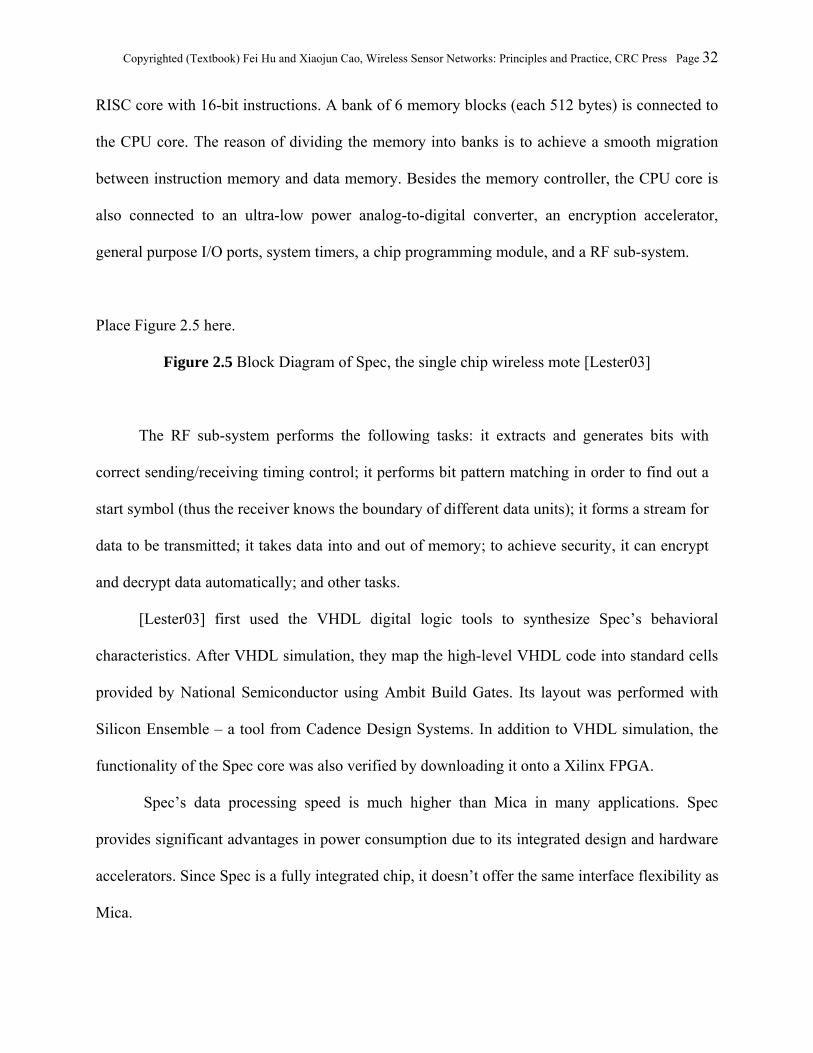
Copyrighted (Textbook) Fei Hu and Xiaojun Cao, Wireless Sensor Networks: Principles and Practice, CRC Press Page 32
RISC core with 16-bit instructions. A bank of 6 memory blocks (each 512 bytes) is connected to
the CPU core. The reason of dividing the memory into banks is to achieve a smooth migration
between instruction memory and data memory. Besides the memory controller, the CPU core is
also connected to an ultra-low power analog-to-digital converter, an encryption accelerator,
general purpose I/O ports, system timers, a chip programming module, and a RF sub-system.
Place Figure 2.5 here.
Figure 2.5 Block Diagram of Spec, the single chip wireless mote [Lester03]
The RF sub-system performs the following tasks: it extracts and generates bits with
correct sending/receiving timing control; it performs bit pattern matching in order to find out a
start symbol (thus the receiver knows the boundary of different data units); it forms a stream for
data to be transmitted; it takes data into and out of memory; to achieve security, it can encrypt
and decrypt data automatically; and other tasks.
[Lester03] first used the VHDL digital logic tools to synthesize Spec’s behavioral
characteristics. After VHDL simulation, they map the high-level VHDL code into standard cells
provided by National Semiconductor using Ambit Build Gates. Its layout was performed with
Silicon Ensemble – a tool from Cadence Design Systems. In addition to VHDL simulation, the
functionality of the Spec core was also verified by downloading it onto a Xilinx FPGA.
Spec’s data processing speed is much higher than Mica in many applications. Spec
provides significant advantages in power consumption due to its integrated design and hardware
accelerators. Since Spec is a fully integrated chip, it doesn’t offer the same interface flexibility as
Mica.
Copyrighted (Textbook) Fei Hu and Xiaojun Cao, Wireless Sensor Networks: Principles and Practice, CRC Press Page 33
2.5 - COTS Dust Systems [Seth00]
In [Seth00], several interesting sensor systems were built. Its mote used the Atmel
AT90LS8535 (as the microcontroller) and RF Monolithics 916MHz RF transceiver. The mote
controls 7 different types of analog sensors (temperature, light, barometric pressure, 2-axis
acceleration, and 2-axis magnetometers). Regarding the power source, it uses a single 3-V
lithium coin cell battery. It can operate for five days of continuous operation or 1.5 years at 1%
duty cycling.
It uses a slow CPU, Atmel MCU with 149.475 KHz. It creates 19 instructions to send
and receive raw data bits through the RF system. Each clock cycle only executes one instruction.
Thus its raw data rate is 149.475 KHz/ 19Cycles/bit = 7.867 Kbps.
In wireless environments, noise / interference can damage packets of data. [seth00] uses
cyclic redundancy check (CRC) to check packet bit errors.
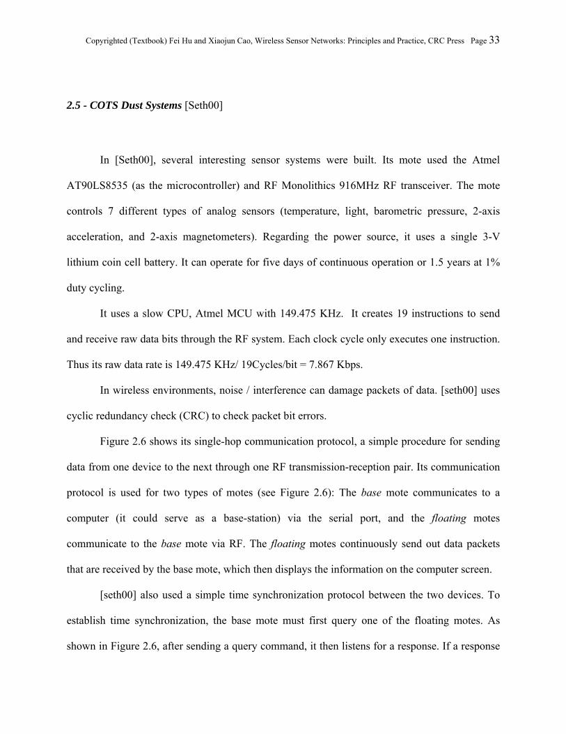
Figure 2.6 shows its single-hop communication protocol, a simple procedure for sending
data from one device to the next through one RF transmission-reception pair. Its communication
protocol is used for two types of motes (see Figure 2.6): The base mote communicates to a
computer (it could serve as a base-station) via the serial port, and the floating motes
communicate to the base mote via RF. The floating motes continuously send out data packets
that are received by the base mote, which then displays the information on the computer screen.
[seth00] also used a simple time synchronization protocol between the two devices. To
establish time synchronization, the base mote must first query one of the floating motes. As
shown in Figure 2.6, after sending a query command, it then listens for a response. If a response
Copyrighted (Textbook) Fei Hu and Xiaojun Cao, Wireless Sensor Networks: Principles and Practice, CRC Press Page 34
is not heard after 100 ms, it proceeds to send out another transmit query. Such a query procedure
is repeated until a valid message is received. Once received, the message is sent from the base
mote to the computer over the serial port. The base mote then proceeds to listen for the next
packet of data.
Figure 2.6 also shows that both protocols have listening periods right after transmission
periods. This enables motes to respond to queries right away. A handshaking protocol enables
both motes to communicate with one another as quickly as possible.
Place Figure 2.6 here.
Figure 2.6 - Protocols used for Base and Floating Mote [seth00]
2.5.1 - Design Advice: Failures and Successes
There are some good lessons summarized in [seth00]:
On the selection of CPU and RF transceiver: In the beginning [seth00] used Scenix
SX28AC series microprocessor that operates with clock cycles up to 50 MHz. However, when
Case Study
[seth00] only presents a very basic mote design without considering many other WSN application requirements. For instance, it doesn’t support multi-hop communication well. Its CPU/transceiver design still has large space to use more energy-efficient interface design. The reason we include its example here is to show that even for a simple mote prototype design, there could be many lessons to learn. (Please see the end of this section on some lessons learned from [seth00]).

Copyrighted (Textbook) Fei Hu and Xiaojun Cao, Wireless Sensor Networks: Principles and Practice, CRC Press Page 35
the first circuit board was populated, there was trouble getting the RF Monolithics transceiver
chipset to work in the presence of the Scenix microprocessor.
[seth00] found out why the transceiver chipset did not work correctly. The RF transceiver
was saturated with noise generated by the CPU – because the CPU was clocked at a slow speed
of 1 MHz, possibly the fast rise and fall times of the CPU contributed to noise in the receiving
band. The second possible reason is that the circuit board did not contain a ground or power
plain. Ground and power planes in circuit boards help to isolate signals from one another and
maintain a stable power supply voltage.
On the choice of power supplies: The Scenix CPU operated at 5 volts and the RFM chips
operated at 3 volts. A way is needed to generate both power supplies. An possible way is to use 3
alkaline batteries to provide 3 and 4.5 volts. Unfortunately the batteries could lose voltage over
their lifetime. The idea of using two voltage converters for both the MCU and the transceiver
chip set was also unappealing due to the added complexity and increased component count. To
solve the problem, [seth00] aimed to use a single operating voltage, namely that of a 3 volt
lithium ion battery. All components were designed to operate within the battery range of 2.75 to
3.25 volts.
2.6 - Telos mote [Joseph05]
The Telos- series mote (such as Telos-B) is a popularly used sensor platform today.
Unlike Spec that integrates the design into silicon, Telos uses COTS components with hardware
accelerators to build a power efficient system that does not sacrifice performance.
Table 2.7 summarizes the main features of different motes.
Copyrighted (Textbook) Fei Hu and Xiaojun Cao, Wireless Sensor Networks: Principles and Practice, CRC Press Page 36
Place Table 2.7 here.
Table 2.7 - The family of Berkeley motes preceding Telos and their capabilities [Joseph05]
After comparing the CPU performance from Atmel, Motorola, and Microchip, Telos
developers select MSP430 CPU due to its following advantages:
(1) It has lowest power consumption in sleep and active modes (see Table 2.7).
(2) It can tolerate a low operation voltage of 1.8V. A low-voltage operation could help to
extract all of the energy out of a power source. If we use AA batteries, they have a cut-
off voltage of 0.9V. A Telos mote uses two batteries. Then the system cut-off voltage
will be 1.8V, which is exactly the minimum required voltage for the MSP430. If we
use other CPUs, say ATmega128 MCU (Mica family), it can only run down to 2.7V,
leaving almost 50% of the AA batteries unused.
(3) We know that a faster wake-up time helps to conserve energy. Table 2.8 shows that
the MSP430 has the fastest wakeup time (it takes <6μs to transition from standby
(1μA) to active mode).
(4) From memory viewpoint, Table 2.8 shows that the MSP430 has the largest on-chip
RAM buffer (10kB). It is good for on-chip signal processing. A larger RAM allows
more sophisticated applications.
From RF communication viewpoint, Telos has the following features:
(1) It uses the IEEE 802.15.4 standard. Such a standardized radio allows a Telos to
communicate with many radio devices from other vendors.
Copyrighted (Textbook) Fei Hu and Xiaojun Cao, Wireless Sensor Networks: Principles and Practice, CRC Press Page 37
(2) It uses the Chipcon CC2420 radio. It uses 2.4GHz RF band, a wideband radio with O-
QPSK modulation with DSSS at 250kbps. Such a high data rate (other motes typically
operates under 150kbps) shortens the operation time (which helps to reduce energy
consumption).
Telos mote can be programmed through on-board USB that also provides power. USB
interface is better than RS232-based serial interface considering that many people use laptops
(that have a few USB ports) to program a mote.
Telos mote has a user button, reset button, and 16-pin IDC expansion header. A
programmer can re-task the reset button as a non-maskable interrupt, thus allowing it to be used
as a power button instead. A developer can also export I2C and UART over the 16-pin IDC
expansion header, in order to attach many connections found on today’s legacy “Mica-style”
sensor boards [JPolastre04].
In many cases we need hardware write protection to protect the good program images in a
memory. Such a write protection also prevents possible write errors when using an over-the-air
programming, which is used in some advanced motes. Telos is the first mote to include hardware
write protection for external storage. The write protection is disabled if plugged into a USB
interface. When running on batteries (without USB), the memory is write protected.
Telos mote has some “sub-circuit” with separate power on/off switch. If any failure is
detected, we could power off a sub-circuit instead of the whole system. Such a power protection
is based on the lessons learned from a real-world WSN application on Great Duck Island (GDI)
[RSzewczyk04]. In GDI application, a failed sensor was caused by a small part of circuit. Since
the failure can be recognized in software, the ability to cut power to that section of the board may
have saved the system as a whole.
Copyrighted (Textbook) Fei Hu and Xiaojun Cao, Wireless Sensor Networks: Principles and Practice, CRC Press Page 38
2.7 - CargoNet [Mateusz07]
In [Mateusz07] a mote called CargoNet is designed to bridge the gap between WSNs and
radio frequency identification (RFID). CargoNet originally targeted applications in
environmental monitoring at the crate level for supply-chain management and asset security. It
uses custom-designed circuits to minimize power consumption and cost.
The CargoNet nodes uses a new concept, called Quasi-Passive Wakeup, to achieve an
asynchronous, multi-modal wakeup, which can wake up (from sleep mode) to perform extremely
low power operations. CargoNet can be used to monitor conditions inside a typical shipping
crate while consuming <25 microwatts of average power.
CargoNet uses external stimuli signals to wake up its sensor mote. This idea is not new
since some other related systems have also explored external wake-up. But CargoNet consumes
much less power than them.
As one example, researchers at Northwestern University have used a similar wake-up
strategy for vibration detection and autonomous crack monitoring. Their platform uses a single
geophone as the input sensor, and wakes up to record aperiodic shocks to ensure structural
integrity of buildings. Although their analog front end consumes only 16.5 μW on average, their
processing is performed by a Mica2 mote, which adds a further 105μW to their average power
budget.
As another example, T-Mote [Tmote06] also has comparators to generate interrupts upon
acoustic or acceleration stimuli, but the use of active accelerometers and microphone amplifiers
consumes much energy (in mW range).

Copyrighted (Textbook) Fei Hu and Xiaojun Cao, Wireless Sensor Networks: Principles and Practice, CRC Press Page 39
In the following, let’s first understand the general concept of RFID.
Radio-frequency identification (RFID) is used to replace traditional bar-code technique to
improve traditional barcodes when used in the transport and distribution of goods. Traditional
bar codes require line-of-sight between interrogator and tagged object. Therefore human
operators must align a tagged object to ensure a successful read. The distance between the
interrogator and bar codes is very short (typically a few centimeters). Moreover, those bar codes
have very short information.
On the other hand, RFID uses a reader to read tags that are attached to products. The
distance between the reader and tags could be even a few inches to over 10 feet long (its range
depends on the used radio frequency). Moreover, the reader can read a tag’s data through non-
light-of-sight signals that propagate widely and permeate through most nonconductive materials,
allowing identification without human involvement. While traditional bar code is printed onto a
surface and cannot be changed, we can change the data in RFID tags since they are electronic
circuits that can change state based on external stimuli.
A concept, called “active RFID”, has been proposed recently. It is actually a special
sensor device with battery and CPUs to provide better “visibility” into their supply chains.
“Active RFIDs” can accurately collect data about environmental conditions experienced by
goods in transit, and better manage risk and maintain flexibility. It can detect potentially
damaged goods before they reach their destination.
CargoNet node is such a type of “active RFID”. Its quasi-passive wakeup is based on the
following interesting fact: the external stimuli could actually be used to wake up and even
provide energy to the CPU!
CargoNet can de-sensitize the sensors following repeating stimuli. This further reduces
Copyrighted (Textbook) Fei Hu and Xiaojun Cao, Wireless Sensor Networks: Principles and Practice, CRC Press Page 40
occurrences of redundant wakeup to save power. Quasi-passive wakeup allows a CargoNet RFID
tag to simultaneously and continuously monitor many sensor modalities for exceptional activity
while dissipating minimal power.
Figure 2.7 is a system diagram with the CargoNet “active RFID” tags and RFID reader. Its
core hardware consists of the MSP430 microcontroller, real-time-clock, and CC2500 2.4GHz
radio. The MSP430F135 flash-based microcontroller is made from Texas Instruments (TI). It has
a specified standby current of less than 0.1µA when entering sleep state.
Place Figure 2.7 here
Figure 2.7 - CargoNet system diagram [Mateusz07]
CargoNet tag has an internal flash memory with a capacity of 16kB. It is a small memory.
But it is big enough for most targeted applications due to two reasons:
(1) Its design allows any memory not dedicated to program storage to be used for data
logging. Its operating system (OS) occupies a very tiny space.
(2) We typically record only extraordinary events (such as extremes of temperature and
significant shocks). The routine code occupies < 8KB. Suppose potentially harmful or
notable events occur once per day and require 10 bytes to log, its flash memory will
last over two years before it is filled!
If a developer needs to test long programs, or in some cases we may need to store more
detailed information in the mote, CargoNet allows the attachment of an external flash memory to
the tag (for instance, Atmel’s AT45DB081B could be attached. It has 8M bits of capacity and a
Copyrighted (Textbook) Fei Hu and Xiaojun Cao, Wireless Sensor Networks: Principles and Practice, CRC Press Page 41
standby current consumption of 2 µA).
MSP430 has internally a fast-starting, high-frequency clock oscillator. A developer can
certainly use external clocks, such as a low-frequency watch crystal. CargoNet suggests
employing a separate Philips PCF8563 real-time clock (RTC) chip, which has a low timekeeping
current (only 0.35 μA). RTC allows an “active RFID” tag to pinpoint where (along the supply
chain) the damage occurred by measuring the time from the last checkpoint. The RTC also
serves to initiate a once-per-minute polling sequence of the humidity and temperature sensors.
The “active RFID” tags use the CC2500 from Chipcon to communicate wirelessly with
RFID readers/interrogators (see Fig 2.7). Different from traditional RFID systems, the CC2500
radio is fully bidirectional, such that the “active RFID” tags can also receive instructions from
the RFID readers besides sending tag data to the reader. This feature bridges the gap between the
“active RFID” and WSNs since WSN motes requires bi-directional communications between
nodes. Such a bi-directional radio communication capability enables useful applications, such as
synchronizing clocks, recording the identity of neighbors, or qualifying the validity of sensor
readings.
When a base-station (it is actually a RFID reader/interrogator in Fig. 2.7) sends out data
query requests to the “active RFID” tags to check significant events (e.g., temperatures or
shocks), request data dumps, or adjust tag parameters, it uses a radio burst signal. CargoNet
motes are able to wake quasi-passively after receiving such an RF amplitude burst at 300 MHz
over a dynamically adjustable threshold.
Note that a CargoNet “active RFID” tag does not typically poll or amplify quickly
changing environmental stimuli. This is for saving energy purpose. Instead, it simply takes
environmental stimuli and compares it against a threshold through “quasi-passive wakeup”
Copyrighted (Textbook) Fei Hu and Xiaojun Cao, Wireless Sensor Networks: Principles and Practice, CRC Press Page 42
technology. The above comparator is based on Linear Technology product (LTC1540). Because
of its nonlinear class-D operation, it typically consumes only 840nW of quiescent power
[Linear04].
But for some stimuli that do not change quickly enough, they may not be able to reach the
“wake-up threshold”. Such stimuli examples have temperature and humidity, etc. For this case,
the “active RFID” tag will poll the stimuli.
An “active RFID” tag uses a 12-bit accuracy sequence to poll the Sensirion SHT11
temperature/humidity sensors. The polling time is around 55ms. If it polls the sensors once a
minute, this corresponds to a duty cycle of only 0.092% and an average power consumption of
1.5μW. Such a low-duty-cycle polling does not dominate the power budget of the tag at all.
If an “active RFID” tag needs to wake up quickly to achieve a very fast response to a
stimulus, say, temperature event, the quasi-passive wakeup on temperature can be
accommodated via a PTC thermistor or other thermal sensors, which exhibit a high impedance
and sharp characteristic response.
CargoNet system also uses the following two sensors, the RF wakeup receiver and
vibration dosimeter. They have linear amplifiers to boost or integrate weak signals.
Table 2.8 lists CargoNet sensors that assemble a suite of measurements relevant to the
transport of equipment and goods.
Place Table 2.8 here.
Table 2.8 - CargoNet sensor types [Mateusz07]

Copyrighted (Textbook) Fei Hu and Xiaojun Cao, Wireless Sensor Networks: Principles and Practice, CRC Press Page 43
Now let’s provide more details on CargoNet’s “Quasi-passive wakeup” strategy. Figure
2.8 shows its basic wake-up procedure. After an “active RFID” tag receives a stimulus signal, it
compares the results against a threshold. If the stimulus is strong enough to warrant interest, the
tag wakes up a larger system.
Place Figure 2.8 here.
Figure 2.8 - The CargoNet system quasi-passive wakeup scheme [Mateusz07]
The above quasi-passive wakeup scheme needs to be built on the following conditions:
(1) An always enabled circuit, i.e., the analog front-end, should consume the order of a
microwatt or less. With milli-volt signal levels, a nanopower comparator (such as the
LTC1540) is needed to boost the stimulus to logic levels and wake the “active RFID”
tag.
(2) In terms of the wake-up time, the “active RFID” tag must wake up fast enough to
adequately process the incoming stimulus. The MSP430, with a 6 μs startup time, is
therefore ideal.
Good Idea
Normally people distinguish RFID from mote very clearly. But CargoNet designs a device that can serve as both RFID tag and a WSN node. It can collect data from environment into a “tag”, and then allow a RFID reader to remotely read such data. The reason we use “active RFID” here is because CargoNet makes its RFID tag battery-driven and have good performance close to an intelligent sensor node.

Copyrighted (Textbook) Fei Hu and Xiaojun Cao, Wireless Sensor Networks: Principles and Practice, CRC Press Page 44
(3) The tag’s duty cycles must be kept very low. This helps to limit the number of
wakeups and the amount of time spent in the active mode.
Besides the high-frequency, faster, longer-range radio for data communication with a
RFID reader, CargoNet “active RFID” tag also has a lower-frequency, shorter-range signaling
channel for interrogation and passing of location information. This is to make it compliant with
other commercial RFID tags that detect the location information.
Due to the shorter range of the low-frequency link, the RF power that is delivered to the
tag is high enough to wake up the tag; then next step - the high-frequency radio, which consumes
up to 20mA of current when using CC2500, is powered on.

Copyrighted (Textbook) Fei Hu and Xiaojun Cao, Wireless Sensor Networks: Principles and Practice, CRC Press Page 45
Problems & Exercises
2.1 Multi-choice questions
(1) A sensor mote includes:
A. Analog / digital sensor chips;
B. RF transceiver;
C. CPU / Memory;
D. All of the above.
(2) The differences between analog sensors and digital sensors do not include which of the
following aspects:
A. Analog sensors need standard chip-to-chip communication protocols to take with CPU
board while digital sensors do not need them.
B. Analog sensors need compensation and linearization; but digital sensors do not need
them.
C. Digital sensors are better choices than analog sensors from CPU interface viewpoint;
D. No ADC (Analog-to-Digital converter) is needed in digital sensor case.
(3) In a sensor network, most of the sensor mote’s energy is typically consumed in:

Copyrighted (Textbook) Fei Hu and Xiaojun Cao, Wireless Sensor Networks: Principles and Practice, CRC Press Page 46
A. Analog sensing part;
B. CPU local calculations on signal processing;
C. Wireless hop-to-hop communications;
D. Wake-up / sleeping transition.
(4) On the CPU in the sensor mote, which of the following is NOT correct?
A. The CPUs used in sensor mote have much weaker capability than general desktop’s or
laptop’s ones. The sensor mote CPUs are often called microprocessors or
microcontrollers.
B. The CPU working frequency in a sensor mote is typically below 100M Hz.
C. When the CPU is in idle/sleep mode, no energy consumption is involved.
D. The main duties of CPU are to execute communication protocols and locally process the
data.
(5) Which of the following is NOT correct on the sensor mote memory?
A. Sensor nodes only require small amounts of storage and program memory.
B. If data is to be stored for long periods of time it is more efficient to use flash instead of
SRAM.
C. The program execution occurs in the flash memory instead of in SRAM.
D. The typical SRAM size is less than 1M bytes so far.

Copyrighted (Textbook) Fei Hu and Xiaojun Cao, Wireless Sensor Networks: Principles and Practice, CRC Press Page 47
(6) The radios on the sensor mote have the following features:
A. Low power radios consume larger energy when in receive than in transmit mode.
B. The sending distance of a wireless system is controlled by several key factors. The most
intuitive factor is that of transmission power.
C. Most RF transceivers on the market today use a VCO (Voltage Controlled Oscillator)-
based radio architecture and have the ability to communicate at a variety of carrier
frequencies.
D. Amplitude modulation (AM) is the simplest to encode and decode, and it is less
susceptible to noise.
(7) In the sender side, which of the following operations is NOT needed?
A. Wait for the receiver’s acknowledgement before sending out next packet;
B. Encode the data by adding error detection bits;
C. Wait for collision free with the help of MAC protocols;
D. Organize sensor data to different packets.
(8) The reason(s) of decoupling between RF and processing speed could be:
A. When the speed of the microcontroller is coupled to the data transmission rate, both
pieces of the system are forced to operate at non-optimal points.

Copyrighted (Textbook) Fei Hu and Xiaojun Cao, Wireless Sensor Networks: Principles and Practice, CRC Press Page 48
B. A radio is most efficient when data transmissions occur at its maximum transmission rate.
When coupling with CPU processing, such efficiency cannot be achieved.
C. RF and CPU are totally different chips and need to be decoupled in most cases.
D. Both A and B.
(9) Spec is better than Mica due to the following reasons:
A. The Mica nodes were constrained by existing inter-chip interfaces. Development of a
custom ASIC allows us to tear down the artificial constraints imposed by commercial
components.
B. It is possible to achieve orders-of-magnitude efficiency improvements on key
communication primitives by using custom silicon.
C. Both A and B.
D. Spec could transmit signals for a longer distance than Mica does.
(10) Which of the following is NOR correct on Telos motes?
A. Telos uses the Bluetooth communication standard (an IEEE 802.15 series), which makes
it suitable for short-range radio communications.
B. Telos uses the MSP430 microcontroller that has the lowest power consumption in sleep
and active modes.
C. Instead of integrating the design into silicon, Telos uses COTS components with
hardware accelerators to build a power efficient system that does not sacrifice
performance.

Copyrighted (Textbook) Fei Hu and Xiaojun Cao, Wireless Sensor Networks: Principles and Practice, CRC Press Page 49
D. Telos is programmed (either with the bootstrap loader or JTAG) through on-board USB
that also provides power.
2.2 Do some Web research to find out the characteristics and design principle of Solar-based
batteries.
2.3 What are the differences between “sensors” and “sensor motes”?
2.4 Read [Mateusz07] and provide more details on the integration of RFID into CargoNet sensor
motes.
2.5 What advantages does the Telos mote have compared to others (such as Mica)?
Discrete Sample VoltageSensor Type Current Time Requirement Manufacturer
Photo 1.9 mA 330 uS 2.7 - 5.5V TaosTemperature 1 mA 400 mS 2.5 - 5.5V Dallas Semiconductor
Humidity 550 uA 300 mS 2.4 - 5.5V SensirionPressure 1 mA 35 mS 2.2 - 3.6V Intersema
Magnetic Fields 4 mA 30 uS Any HoneywellAcceleration 2 mA 10 mS 2.5 - 3.3V Analog Devices
Acoustic 0.5 mA 1 mS 2 - 10V PanasonicSmoke 5 uA -- 6 - 12V Motorola
Passive IR (Motion) 0 mA 1 mS Any MelixisPhotosynthetic Light 0 mA 1 mS Any Li-Cor
Soil Moisture 2 mA 10 mS 2 - 5V Ech2o
Table 2.1
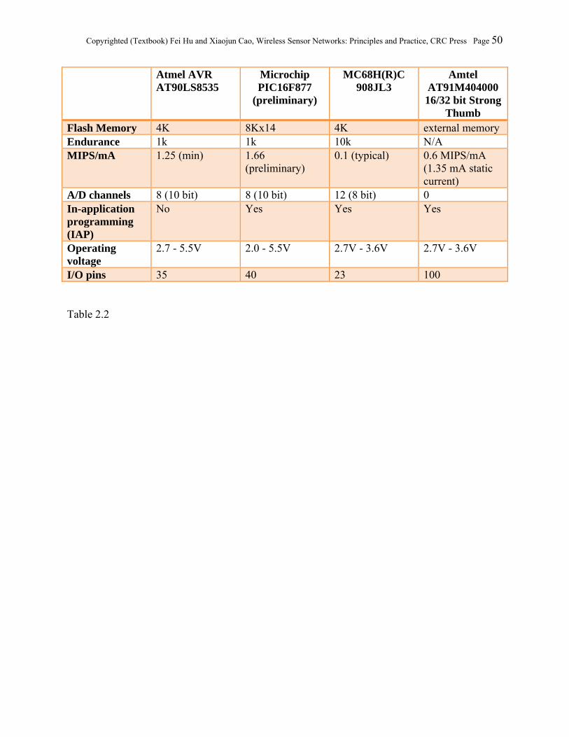
Copyrighted (Textbook) Fei Hu and Xiaojun Cao, Wireless Sensor Networks: Principles and Practice, CRC Press Page 50
Atmel AVR AT90LS8535
Microchip PIC16F877
(preliminary)
MC68H(R)C 908JL3
Amtel AT91M404000 16/32 bit Strong
Thumb Flash Memory 4K 8Kx14 4K external memory Endurance 1k 1k 10k N/A MIPS/mA 1.25 (min) 1.66
(preliminary) 0.1 (typical) 0.6 MIPS/mA
(1.35 mA static current)
A/D channels 8 (10 bit) 8 (10 bit) 12 (8 bit) 0 In-application programming (IAP)
No Yes Yes Yes
Operating voltage
2.7 - 5.5V 2.0 - 5.5V 2.7V - 3.6V 2.7V - 3.6V
I/O pins 35 40 23 100
Table 2.2
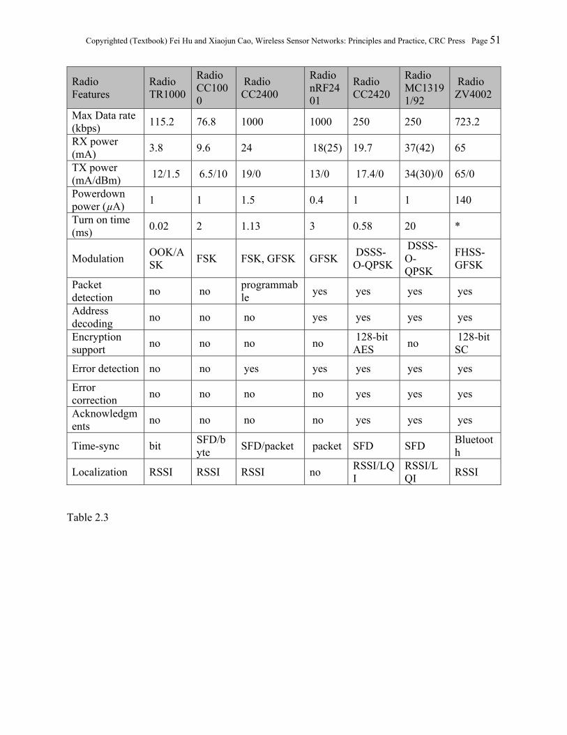
Copyrighted (Textbook) Fei Hu and Xiaojun Cao, Wireless Sensor Networks: Principles and Practice, CRC Press Page 51
Radio Features
Radio TR1000
Radio CC1000
Radio CC2400
Radio nRF2401
Radio CC2420
Radio MC13191/92
Radio ZV4002
Max Data rate (kbps)
115.2 76.8 1000 1000 250 250 723.2
RX power (mA)
3.8 9.6 24 18(25) 19.7 37(42) 65
TX power (mA/dBm)
12/1.5 6.5/10 19/0 13/0 17.4/0 34(30)/0 65/0
Powerdown power (µA)
1 1 1.5 0.4 1 1 140
Turn on time (ms)
0.02 2 1.13 3 0.58 20 *
Modulation OOK/ASK
FSK FSK, GFSK GFSK DSSS-O-QPSK
DSSS-O-QPSK
FHSS-GFSK
Packet detection
no no programmable
yes yes yes yes
Address decoding
no no no yes yes yes yes
Encryption support
no no no no 128-bit AES
no 128-bit SC
Error detection no no yes yes yes yes yes
Error correction
no no no no yes yes yes
Acknowledgments
no no no no yes yes yes
Time-sync bit SFD/byte
SFD/packet packet SFD SFD Bluetooth
Localization RSSI RSSI RSSI no RSSI/LQI
RSSI/LQI
RSSI
Table 2.3
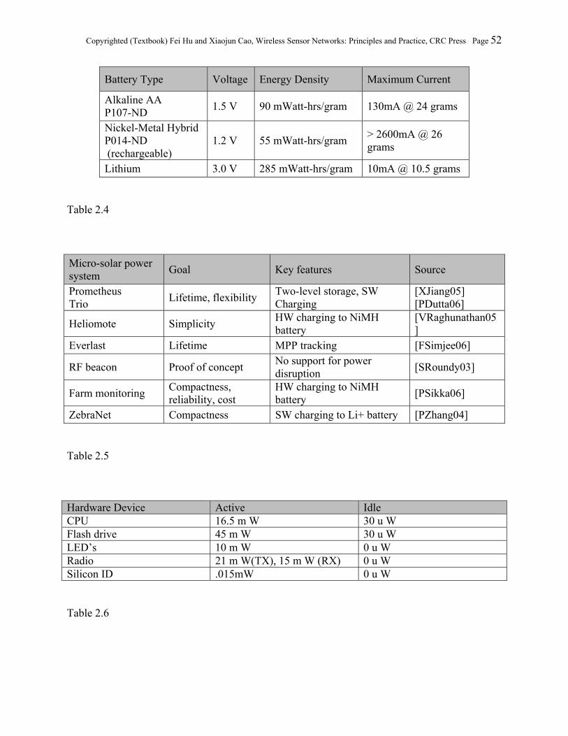
Copyrighted (Textbook) Fei Hu and Xiaojun Cao, Wireless Sensor Networks: Principles and Practice, CRC Press Page 52
Battery Type Voltage Energy Density Maximum Current
Alkaline AA P107-ND
1.5 V 90 mWatt-hrs/gram 130mA @ 24 grams
Nickel-Metal Hybrid P014-ND (rechargeable)
1.2 V 55 mWatt-hrs/gram > 2600mA @ 26 grams
Lithium 3.0 V 285 mWatt-hrs/gram 10mA @ 10.5 grams
Table 2.4
Micro-solar power system
Goal Key features Source
Prometheus Trio
Lifetime, flexibility Two-level storage, SW Charging
[XJiang05] [PDutta06]
Heliomote Simplicity HW charging to NiMH battery
[VRaghunathan05]
Everlast Lifetime MPP tracking [FSimjee06]
RF beacon Proof of concept No support for power disruption
[SRoundy03]
Farm monitoring Compactness, reliability, cost
HW charging to NiMH battery
[PSikka06]
ZebraNet Compactness SW charging to Li+ battery [PZhang04]
Table 2.5
Hardware Device Active Idle CPU 16.5 m W 30 u W Flash drive 45 m W 30 u W LED’s 10 m W 0 u W Radio 21 m W(TX), 15 m W (RX) 0 u W Silicon ID .015mW 0 u W
Table 2.6
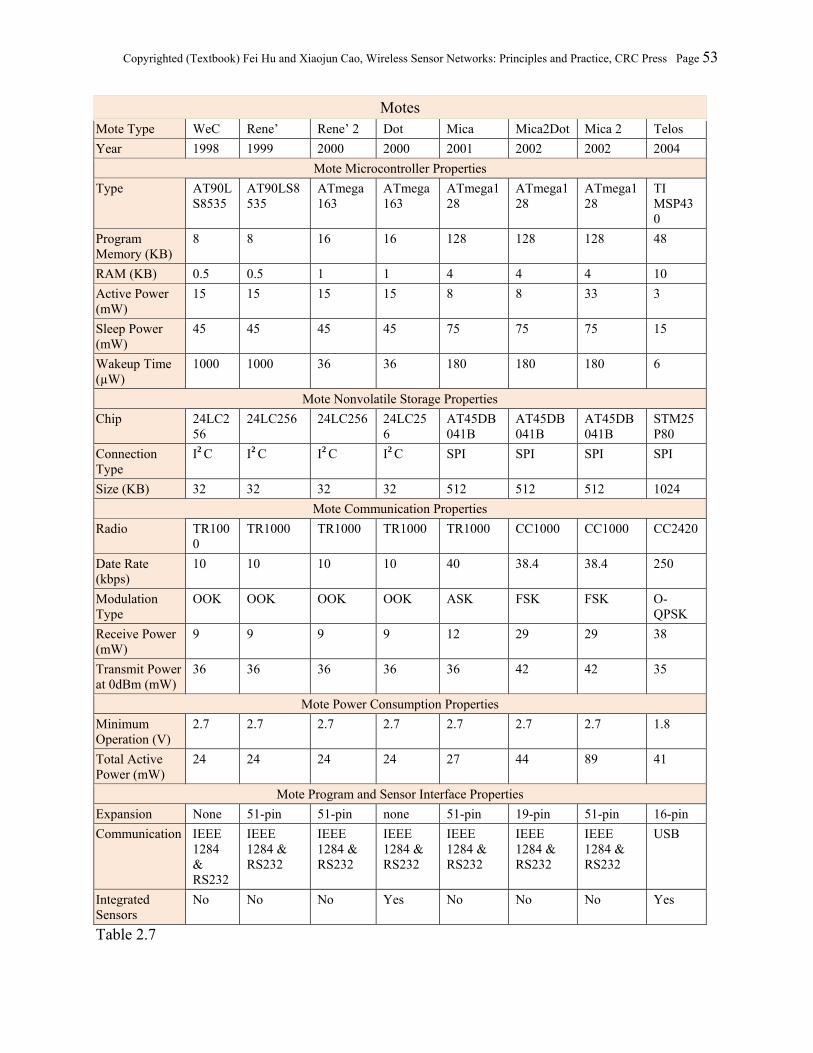
Copyrighted (Textbook) Fei Hu and Xiaojun Cao, Wireless Sensor Networks: Principles and Practice, CRC Press Page 53
Motes Mote Type WeC Rene’ Rene’ 2 Dot Mica Mica2Dot Mica 2 Telos
Year 1998 1999 2000 2000 2001 2002 2002 2004
Mote Microcontroller Properties
Type AT90LS8535
AT90LS8535
ATmega163
ATmega163
ATmega128
ATmega128
ATmega128
TI MSP430
Program Memory (KB)
8 8 16 16 128 128 128 48
RAM (KB) 0.5 0.5 1 1 4 4 4 10
Active Power (mW)
15 15 15 15 8 8 33 3
Sleep Power (mW)
45 45 45 45 75 75 75 15
Wakeup Time (µW)
1000 1000 36 36 180 180 180 6
Mote Nonvolatile Storage Properties
Chip 24LC256
24LC256 24LC256 24LC256
AT45DB041B
AT45DB041B
AT45DB041B
STM25P80
Connection Type
I2 C I2 C I2 C I2 C SPI SPI SPI SPI
Size (KB) 32 32 32 32 512 512 512 1024
Mote Communication Properties
Radio TR1000
TR1000 TR1000 TR1000 TR1000 CC1000 CC1000 CC2420
Date Rate (kbps)
10 10 10 10 40 38.4 38.4 250
Modulation Type
OOK OOK OOK OOK ASK FSK FSK O-QPSK
Receive Power (mW)
9 9 9 9 12 29 29 38
Transmit Power at 0dBm (mW)
36 36 36 36 36 42 42 35
Mote Power Consumption Properties
Minimum Operation (V)
2.7 2.7 2.7 2.7 2.7 2.7 2.7 1.8
Total Active Power (mW)
24 24 24 24 27 44 89 41
Mote Program and Sensor Interface Properties
Expansion None 51-pin 51-pin none 51-pin 19-pin 51-pin 16-pin
Communication IEEE 1284 & RS232
IEEE 1284 & RS232
IEEE 1284 & RS232
IEEE 1284 & RS232
IEEE 1284 & RS232
IEEE 1284 & RS232
IEEE 1284 & RS232
USB
Integrated Sensors
No No No Yes No No No Yes
Table 2.7

Copyrighted (Textbook) Fei Hu and Xiaojun Cao, Wireless Sensor Networks: Principles and Practice, CRC Press Page 54
Sensor Type Measurement or Application
Shock Sensor Potential impact damage
Vibration Dosimeter Average low-level vibrations
Tilt Switch Package orientation and shaking
Piezo Microphone Events causing loud nearby sounds
Light Sensor Container breach or box opening
Magnetic Switch Package removed or box opened
Temperature Sensor Overheating or potential spoilage
Humidity Sensor Potential moisture damage
RF Wakeup Query from reader or another tag
Table 2.8
Recommended