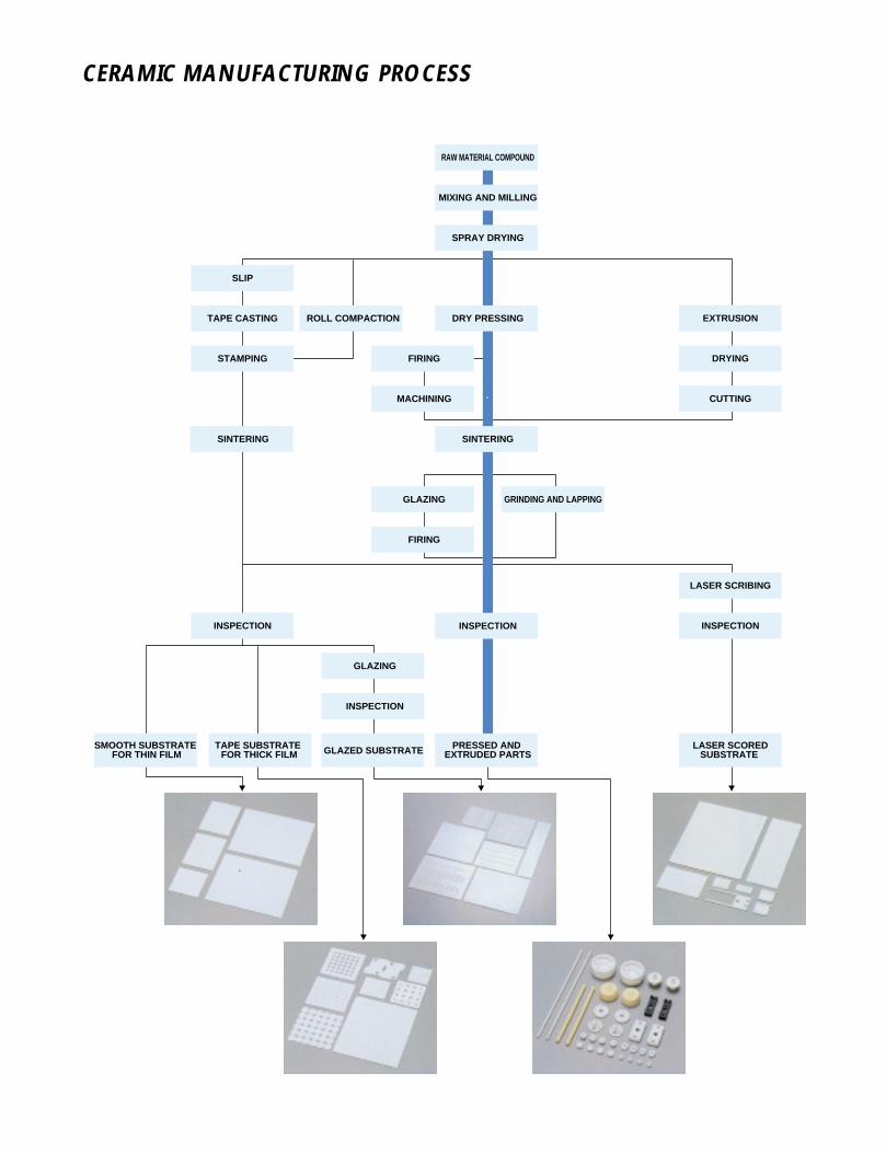
CERAMIC MANUFACTURING PROCESS
SLIP
EXTRUSION
RAW MATERIAL COMPOUND
MIXING AND MILLING
SPRAY DRYING
TAPE CASTING
STAMPING
ROLL COMPACTION DRY PRESSING
FIRING
MACHINING
SINTERING
GLAZING
FIRING
GRINDING AND LAPPING
DRYING
CUTTING
LASER SCRIBING
INSPECTIONINSPECTIONINSPECTION
GLAZING
INSPECTION
SMOOTH SUBSTRATE FOR THIN FILM
SINTERING
TAPE SUBSTRATE FOR THICK FILM GLAZED SUBSTRATE PRESSED AND
EXTRUDED PARTSLASER SCORED
SUBSTRATE
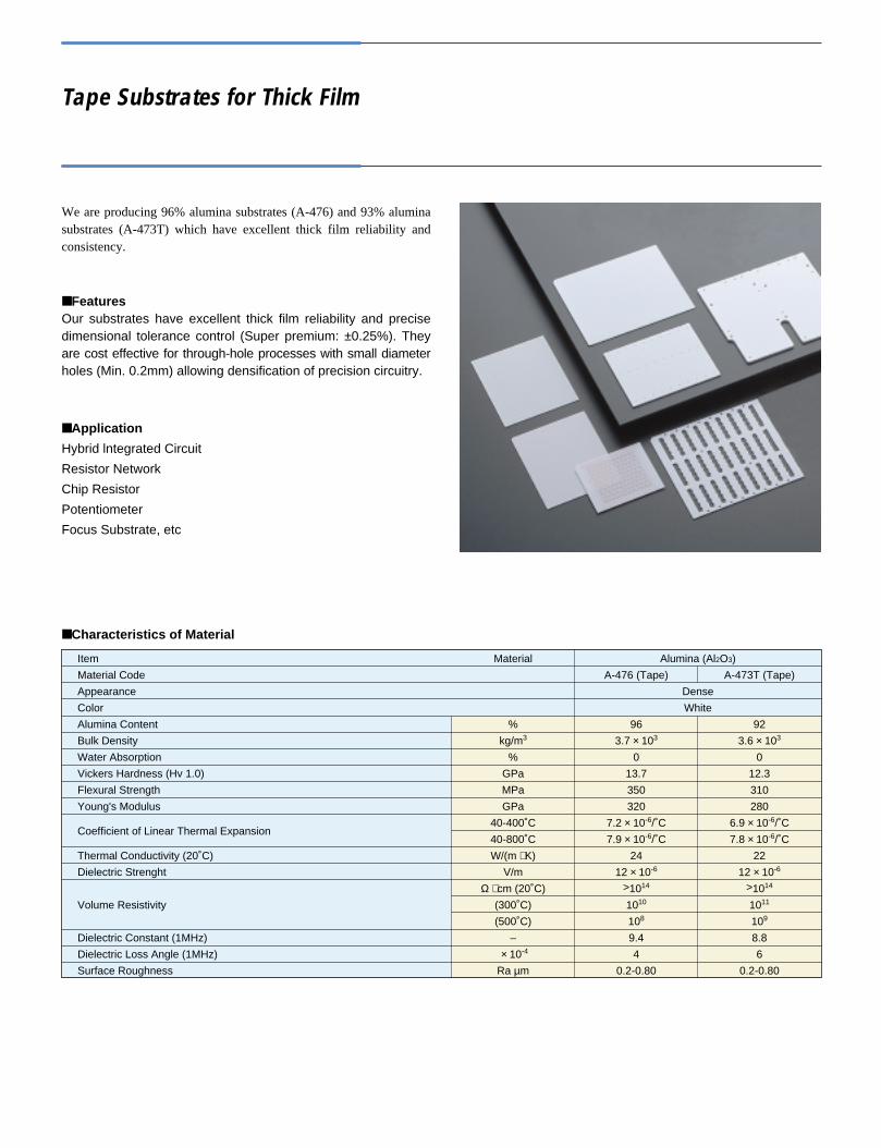
Tape Substrates for Thick Film
We are producing 96% alumina substrates (A-476) and 93% alumina substrates (A-473T) which have excellent thick film reliability and consistency.
FeaturesOur substrates have excellent thick film reliability and precise dimensional tolerance control (Super premium: ±0.25%). They are cost effective for through-hole processes with small diameter holes (Min. 0.2mm) allowing densification of precision circuitry.
Application
Hybrid lntegrated Circuit
Resistor Network
Chip Resistor
Potentiometer
Focus Substrate, etc
Characteristics of Material
Item
Material Code
Appearance
Color
Alumina Content
Bulk Density
Water Absorption
Vickers Hardness (Hv 1.0)
Flexural Strength
Young's Modulus
Coefficient of Linear Thermal Expansion
Thermal Conductivity (20˚C)
Dielectric Strenght
Volume Resistivity
Dielectric Constant (1MHz)
Dielectric Loss Angle (1MHz)
Surface Roughness
Material
%
kg/m3
%
GPa
MPa
GPa
40-400˚C
40-800˚C
W/(m ⋅ K)
V/m
Ω ⋅ cm (20˚C)
(300˚C)
(500˚C)
–
× 10-4
Ra µm
Alumina (Al2O3)
A-476 (Tape)
96
3.7 × 10³
0
13.7
350
320
7.2 × 10⁻⁶/˚C
7.9 × 10⁻⁶/˚C
24
12 × 10-6
>1014
1010
108
9.4
4
0.2-0.80
A-473T (Tape)
92
3.6 × 10³
0
12.3
310
280
6.9 × 10⁻⁶/˚C
7.8 × 10⁻⁶/˚C
22
12 × 10-6
>1014
1011
109
8.8
6
0.2-0.80
Dense
White
Features Uniform grain size and small voids Equivalent to A-476 for thick film characteristics Less camber and edge-curl Larger size can be produced (Max. 8" × 10") Tight tolerance:Standard: ±0.5% Premium: ±0.25% Same surface roughness on both sides
Application Thick film hybrid IC Focus substrate, and others
Design Guideline Unit: Inch (mm)
A-473T (93% Alumina)
Surface Roughness
Manufacturing Method
As Fired Camber
Thickness Availability
Thickness Tolerance
Size Availability
Length & Width Tolerance
Scribing Tolerance
Parallelism
Perpendicularity
Corner R
Hole Size
Spacing Between Holes
or Edge to Holes
Surface Roughness
Tape
A-476: 8 to 30 µ inch CLA (Ra 0.2-0.75 µ m)
A-473T: 8 to 30 µ inch CLA (Ra 0.2-0.75 µ m)
Punched/Greenscored
Standard:±0.8%NLT±.004 (0.10)Premium:±0.5%NLT±.003 (0.08)
Super Premium: ±0.25%NLT±.002 (0.05)
Standard:±0.8%NLT±.004 (0.10)Premium:±0.5%NLT±.003 (0.08)
Super Premium: ±0.25%NLT±.002 (0.05)
Standard:0.5% of outside dim.
Premium:0.3% of outside dim.
.020 (0.51)
.008 (0.20) Dia. Min.
.015 (0.38) Square Min.
Minimum equal to
thickness of substrate
NLT±.020 (0.51)
Laser Scored
+.008 (0.20)–.002 (0.05)
Edge to Scoreline:+.008 (0.20) –.002 (0.05)
Scoreline to Scoreline: ±.002 (0.05)
±.002 (0.05)
*
*
*
SEM (A-473T)
5.00 µm
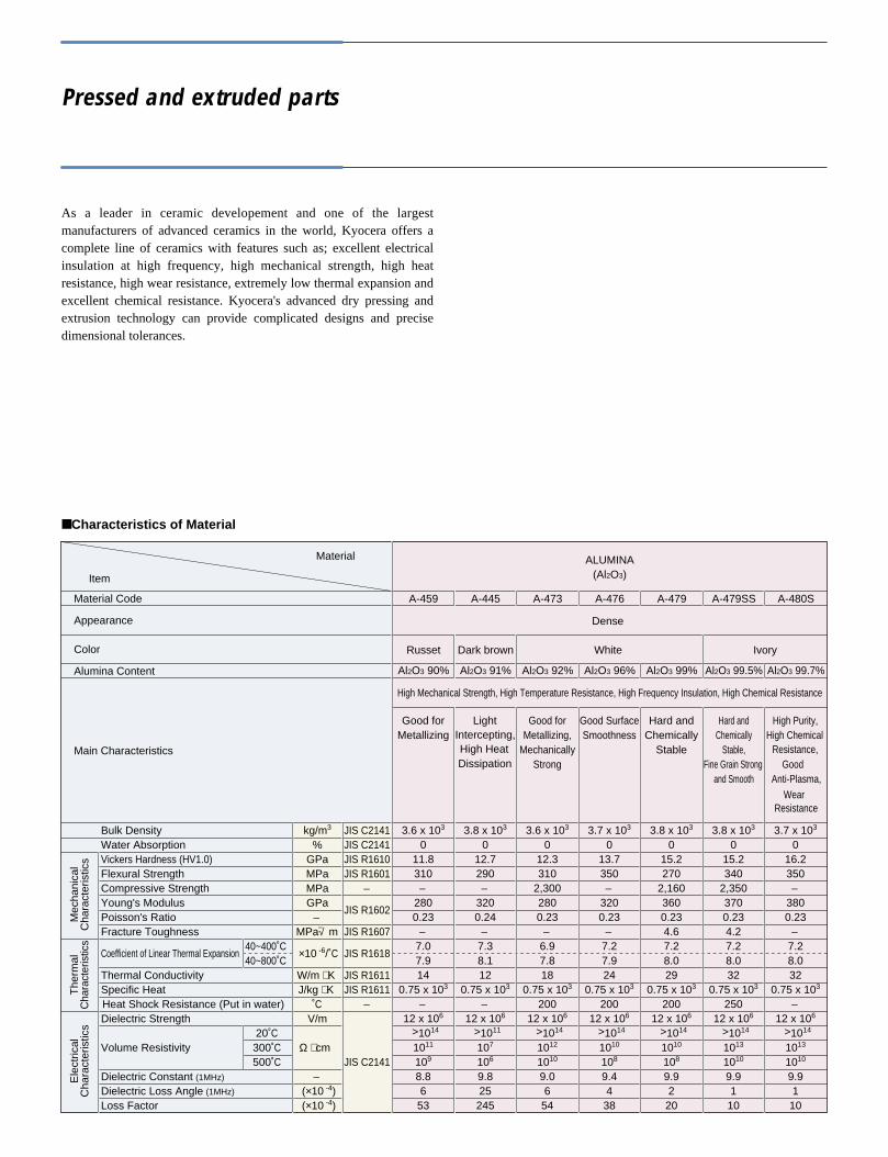
Pressed and extruded parts
As a leader in ceramic developement and one of the largest manufacturers of advanced ceramics in the world, Kyocera offers a complete line of ceramics with features such as; excellent electrical insulation at high frequency, high mechanical strength, high heat resistance, high wear resistance, extremely low thermal expansion and excellent chemical resistance. Kyocera's advanced dry pressing and extrusion technology can provide complicated designs and precise dimensional tolerances.
Characteristics of Material
Material
Item
Material Code
Appearance
Color
Alumina Content
Main Characteristics
Bulk DensityWater AbsorptionVickers Hardness (HV1.0)Flexural StrengthCompressive StrengthYoung's ModulusPoisson's RatioFracture Toughness 40~400˚CCoefficient of Linear Thermal Expansion
40~800˚CThermal ConductivitySpecific Heat Heat Shock Resistance (Put in water)Dielectric Strength 20˚CVolume Resistivity 300˚C 500˚CDielectric Constant (1MHz)
Dielectric Loss Angle (1MHz)
Loss Factor
kg/m3
%GPaMPaMPaGPa
–MPa√ m
×10 -6/˚C
W/m ⋅ KJ/kg ⋅ K
˚CV/m
Ω ⋅ cm
–(×10 -4)(×10 -4)
JIS C2141JIS C2141JIS R1610JIS R1601
–
JIS R1602
JIS R1607
JIS R1618
JIS R1611JIS R1611
–
JIS C2141
Mec
hani
cal
Cha
ract
eris
tics
Ele
ctric
alC
hara
cter
istic
sT
herm
alC
hara
cter
istic
s
A-459
Al2O3 90% Al2O3 91% Al2O3 92% Al2O3 96% Al2O3 99% Al2O3 99.5% Al2O3 99.7%
Russet Dark brown White Ivory
A-445 A-473 A-476 A-479 A-479SS A-480S
High Purity,High Chemical
Good
Wear
Hard andChemically
Stable,Fine Grain Strong
and Smooth
Hard andChemically
Stable
Good SurfaceSmoothness
Good forMetallizing,
MechanicallyStrong
Light
High HeatDissipation
Good forMetallizing
3.6 x 10³
011.8310–
2800.23
–7.07.914
0.75 x 10³
–12 x 106
>1014
1011
109
8.8653
3.8 x 10³
012.7290–
3200.24
–7.38.112
0.75 x 10³
–12 x 106
>1011
107
106
9.825245
3.6 x 10³
012.3310
2,3002800.23
–6.97.818
0.75 x 10³
20012 x 106
>1014
1012
1010
9.0654
3.7 x 10³
013.7350–
3200.23
–7.27.924
0.75 x 10³
20012 x 106
>1014
1010
108
9.4438
3.8 x 10³
015.2270
2,1603600.234.67.28.029
0.75 x 10³
20012 x 106
>1014
1010
108
9.9220
3.8 x 10³
015.2340
2,3503700.234.27.28.032
0.75 x 10³
25012 x 106
>1014
1013
1010
9.9110
3.7 x 10³
016.2350–
3800.23
–7.28.032
0.75 x 10³
–12 x 106
>1014
1013
1010
9.91
10
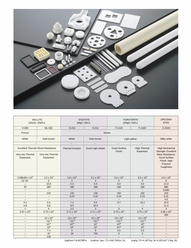
ALUMINA(Al2O3)
Dense
High Mechanical Strength, High Temperature Resistance, High Frequency Insulation, High Chemical Resistance
Resistance,
Anti-Plasma,
Resistance
Intercepting,
K-690 ML-652
White Dark brown
High MechanicalStrength, ExcellentWear Resistance,
Good SurfaceFinish, High
FractureToughness
MULLITE(3Al2O3 ⋅ 2SiO2)
DensePorous
Excellent Thermal Shock Resistance
–
Very low ThermalExpansion
Thermal Insulator Good Light Shield
Very low ThermalExpansion
High ThermalExpansion
2.0(Bulk) x 103
10~20–
30––––
4.14.81
0.67 x 10³
––––––––
6.0 x 10³
012.3980
5,6902100.314.5
10.511.0
30.46 x 10³
300–––––––
3.2 x 10³
010.8280
–210
––
5.05.85
0.75 x 10³
–12 x 106
>10 14
1012
109
7.420
148
S-210 S-211 F-1023
White Dark brown Milky whiteLight yellow
STEATITE(MgO ⋅ SiO2)
FORSTERITE(2MgO ⋅ SiO2)
2.8 x 10³
05.4180
–1200.24
–7.48.02.2
0.71 x 10³
–13 x 106
>10 14
1010
107
618–
3.1 x 10³
06.4180
–1300.22
–9.2
10.42
0.71 x 10³
–13 x 106
>10 14
107
107
8750
–
3.0 x 10³
06.9160
–1500.24
–9.7–5
0.75 x 10³
–13 x 106
>10 14
1010
1010
6.55–
3.0 x 10³
05.9160
–1500.24
–10.1
–5
0.75 x 10³
–13 x 106
>10 14
109
109
6.55–
– – – – –
Good SurfaceFinish
F-1120
ZIRCONIA(PSZ)
Z-201N
1kgf/mm 2=9.807MPa 1cal/cm ⋅ sec ⋅ ˚C=418.7W/(m ⋅ k) 1cal/g ⋅ C=4.187J/g ⋅ K=4.187x10 3J (kg ⋅ K)
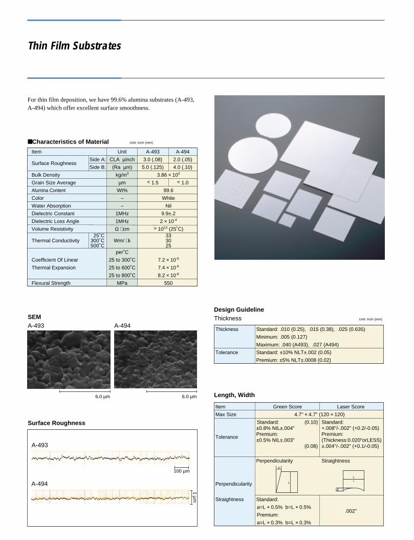
Thin Film Substrates
For thin film deposition, we have 99.6% alumina substrates (A-493, A-494) which offer excellent surface smoothness.
Characteristics of Material Unit: Inch (mm)
Length, Width
Design GuidelineThickness Unit: Inch (mm)
Item Unit A-493 A-494
Side A: CLA µinch 3.0 (.08) 2.0 (.05)Surface Roughness
Side B: (Ra µm) 5.0 (.125) 4.0 (.10)
Bulk Density kg/m3 3.86 × 10³
Grain Size Average µm < 1.5 < 1.0
Alumina Content Wt% 99.6
Color – White
Water Absorption – Nil
Dielectric Constant 1MHz 9.9±.2
Dielectric Loss Angle 1MHz 2 × 10⁻⁴
Volume Resistivity Ω ⋅ cm > 1014 (25˚C)25˚C 33
Thermal Conductivity 300˚C Wm/ ⋅ k 30500˚C 25
per˚C
Coefficient Of Linear 25 to 300˚C 7.2 × 10⁻⁶
Thermal Expansion 25 to 600˚C 7.4 × 10⁻⁶
25 to 800˚C 8.2 × 10⁻⁶
Flexural Strength MPa 550
SEMA-493 A-494
6.0 µm 6.0 µm
Surface Roughness
Thickness Standard: .010 (0.25), .015 (0.38), .025 (0.635)
Minimum: .005 (0.127)
Maximum: .040 (A493), .027 (A494)
Tolerance Standard: ±10% NLT±.002 (0.05)
Premium: ±5% NLT±.0008 (0.02)
Item Green Score Laser Score
Max Size 4.7" × 4.7" (120 × 120)
Standard: (0.10) Standard:±0.8% NIL±.004" +.008"/-.002" (+0.2/-0.05)
Tolerance Premium: Premium:±0.5% NIL±.003" (Thickness:0.020"orLESS) (0.08) ±.004"/-.002" (+0.1/-0.05)
Perpendicularity Straightness
Perpendicularity
Straightness Standard:
a=L × 0.5% b=L × 0.5%.002"
Premium:
a=L × 0.3% b=L × 0.3%
a
L
b
L
A-493
A-494
100 µm
1 µm
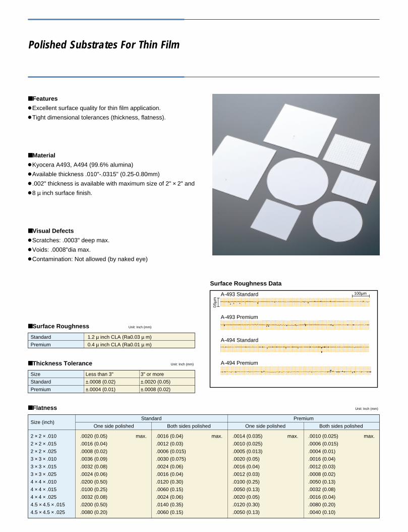
Polished Substrates For Thin Film
Features Excellent surface quality for thin film application. Tight dimensional tolerances (thickness, flatness).
Material Kyocera A493, A494 (99.6% alumina) Available thickness .010"-.0315" (0.25-0.80mm) .002" thickness is available with maximum size of 2" × 2" and 8 µ inch surface finish.
Visual Defects Scratches: .0003" deep max. Voids: .0008"dia max. Contamination: Not allowed (by naked eye)
Surface Roughness Unit: Inch (mm)
Thickness Tolerance Unit: Inch (mm)
Flatness Unit: Inch (mm)
Standard 1.2 µ inch CLA (Ra0.03 µ m)
Premium 0.4 µ inch CLA (Ra0.01 µ m)
Size Less than 3" 3" or more
Standard ±.0008 (0.02) ±.0020 (0.05)
Premium ±.0004 (0.01) ±.0008 (0.02)
Standard PremiumSize (inch)
One side polished Both sides polished One side polished Both sides polished
2 × 2 × .010 .0020 (0.05) max. .0016 (0.04) max. .0014 (0.035) max. .0010 (0.025) max.
2 × 2 × .015 .0016 (0.04) .0012 (0.03) .0010 (0.025) .0006 (0.015)
2 × 2 × .025 .0008 (0.02) .0006 (0.015) .0005 (0.013) .0004 (0.01)
3 × 3 × .010 .0036 (0.09) .0030 (0.075) .0020 (0.05) .0016 (0.04)
3 × 3 × .015 .0032 (0.08) .0024 (0.06) .0016 (0.04) .0012 (0.03)
3 × 3 × .025 .0024 (0.06) .0016 (0.04) .0012 (0.03) .0008 (0.02)
4 × 4 × .010 .0200 (0.50) .0120 (0.30) .0100 (0.25) .0050 (0.13)
4 × 4 × .015 .0100 (0.25) .0060 (0.15) .0050 (0.13) .0032 (0.08)
4 × 4 × .025 .0032 (0.08) .0024 (0.06) .0020 (0.05) .0016 (0.04)
4.5 × 4.5 × .015 .0200 (0.50) .0140 (0.35) .0120 (0.30) .0080 (0.20)
4.5 × 4.5 × .025 .0080 (0.20) .0060 (0.15) .0050 (0.13) .0040 (0.10)
Surface Roughness Data
A-493 Standard
A-493 Premium
A-494 Standard
A-494 Premium
100µm
0.5µ
m
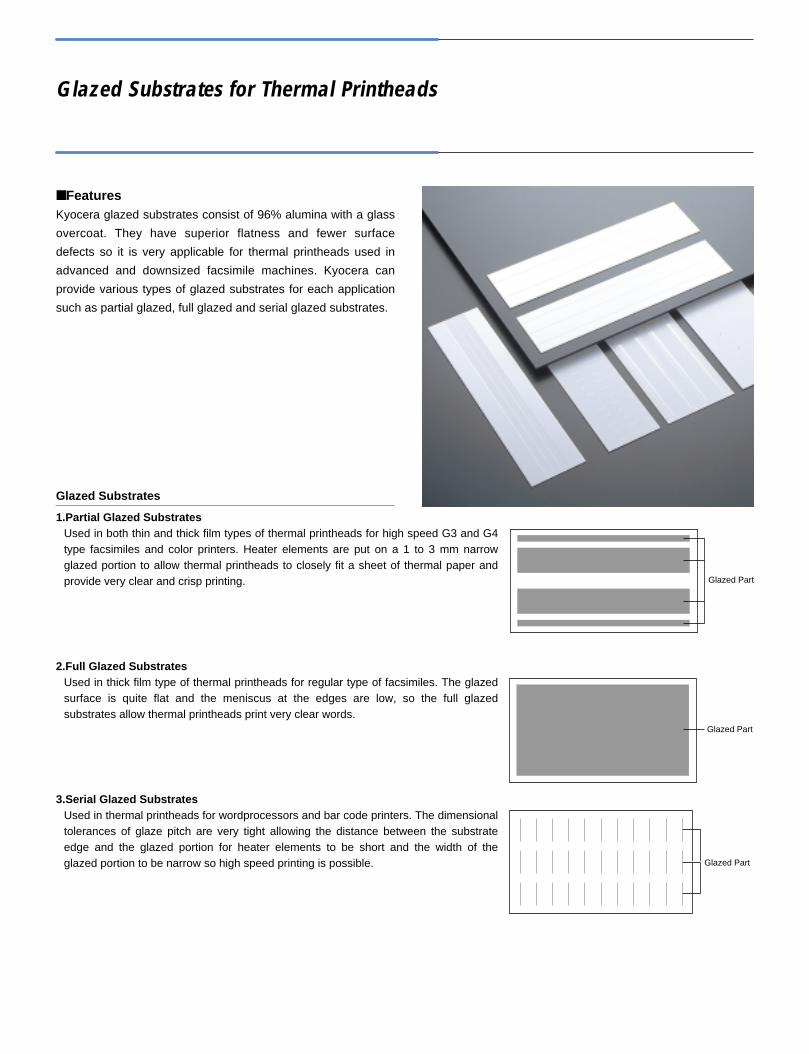
Glazed Substrates for Thermal Printheads
FeaturesKyocera glazed substrates consist of 96% alumina with a glass
overcoat. They have superior flatness and fewer surface
defects so it is very applicable for thermal printheads used in
advanced and downsized facsimile machines. Kyocera can
provide various types of glazed substrates for each application
such as partial glazed, full glazed and serial glazed substrates.
Glazed Part
Glazed Part
Glazed Part
Glazed Substrates
1.Partial Glazed SubstratesUsed in both thin and thick film types of thermal printheads for high speed G3 and G4 type facsimiles and color printers. Heater elements are put on a 1 to 3 mm narrow glazed portion to allow thermal printheads to closely fit a sheet of thermal paper and provide very clear and crisp printing.
2.Full Glazed SubstratesUsed in thick film type of thermal printheads for regular type of facsimiles. The glazed surface is quite flat and the meniscus at the edges are low, so the full glazed substrates allow thermal printheads print very clear words.
3.Serial Glazed SubstratesUsed in thermal printheads for wordprocessors and bar code printers. The dimensional tolerances of glaze pitch are very tight allowing the distance between the substrate edge and the glazed portion for heater elements to be short and the width of the glazed portion to be narrow so high speed printing is possible.
Glazed Substrate Material Specification
Glazed Substrate Design Guideline Unit: Inch (mm)
Item Unit Condition GS-5 GS-71
Glass Transition Temperature ˚C – 669 680
Glass Softening Temperature ˚C – 856 870
Coefficient of Linear Thermal Expansion 1/˚C R. T. to 400˚C 6.6 × 10⁻⁶ 6.8 × 10⁻⁶
Thermal Conductivity W/m ⋅ k 20˚C 0.83 0.75
20˚C >1014 >1014
Volume Resistivity Ω ⋅˚C 300˚C >1014 >1014
500˚C 2.8 × 10¹⁰ 2.1 × 10¹⁰
Dielectric Constant – 1MHz 20˚C 7.2 8.7
Dielectric Loss Angle – 1MHz 20˚C 14.6 × 10⁻⁴ 10.0 × 10⁻⁴
Surface Roughness Ra µm <0.02 <0.02
Item STD Dimensions STD Tolerance Premium Tolerance
.025 (0.635) ±.0024 (±0.06) ±.0016 (±0.04)
Thickness .032 (0.800) ±.0032 (±0.08) ±.0024 (±0.06)
.040 (1.000) ±.0040 (±0.10) ±.0032 (±0.08)
L:12.44 max.
Outside Dimensions (316 max.) ±.080 (±0.20) ±.040 (±0.10)
W:3.15 max.
(80 max.) ±.080 (±0.20) ±.040 (±0.10)
.024 max. (0.6 max.) .020 max. (0.5 max.)Thickness Full Glaze
Camber
.025/.032
.020 max. (0.5 max.) .016 max. (0.4 max.)
Substrate Size: 9 × 3.1 (230 × 80)
(0.635/0.8) Partial Glaze
Glaze Thickness: .0027 (70 µm) .020 max. (0.5 max.) .016 max. (0.4 max.)Thickness
Full Glaze
.040 (1.0)t.016 max. (0.4 max.) .012 max. (0.3 max.)Partial Glaze
Full Glaze:
.0018 to .0032 ±.0006 (±15µm) ±.0004 (±10µm)
Glaze Thickness (45 to 80µm)
Partial Glaze:
.0012 to .0024 ±.0004 (±10µm) ±.00028 (±7µm)
(30 to 60µm)
.120" from all edges .0008 max. /.120 .0006 max. /.120Meniscus of Full Glazed Substrates
(3mm) (20µm max./3mm) (15µm max./3mm)
Glaze thickness of partial glazed substrate with width of less than .035" is .002" max.
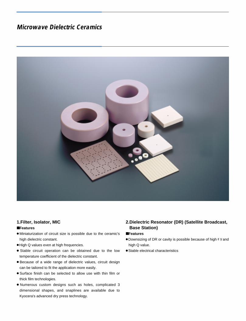
Microwave Dielectric Ceramics
1.Filter, Isolator, MIC Features Miniaturization of circuit size is possible due to the ceramic's
high dielectric constant. High Q values even at high frequencies. Stable circuit operation can be obtained due to the low
temperature coefficient of the dielectric constant. Because of a wide range of dielectric values, circuit design
can be tailored to fit the application more easily. Surface finish can be selected to allow use with thin film or
thick film technologies. Numerous custom designs such as holes, complicated 3
dimensional shapes, and snaplines are available due to
Kyocera's advanced dry press technology.
2.Dielectric Resonator (DR) (Satellite Broadcast, Base Station) Features Downsizing of DR or cavity is possible because of high ε γ and
high Q value. Stable electrical characteristics
Characteristics of Material
Material Code SM200 SM210 SH790 SH890 SH110 SB350 SL390 SV430
Dielectric Constant εγ 20±1 21±1 79±1 89±1 110±3 35~37 39~42 43~46
Q value (GHz)>8000 >8000 >1500 >1800 >1200 4500 6500 4400
(6) (6) (2.6) (2.6) (2.3) (10) (10) (10)
ppm/˚Cτ ε τ ε τ ε τ ε τ ε τ f τ f τ f
Temperature Coefficient (τ ε or τ f)-25±30 -25±30 -35±30 -35±30 -70±30 0±1~8±1 -3±1~8±1 -7±1~8±1
1/˚C 9.2 × 10⁻⁶ 9.2 × 10⁻⁶ 10.1 × 10⁻⁶ 10.1 × 10⁻⁶ 10.1 × 10⁻⁶ 9.0 × 10⁻⁶ 10.3 × 10⁻⁶ 10.2 × 10⁻⁶Coefficient of Linear Thermal Expansion (40~400˚C)
Thermal Conductivity W/m ⋅ k 7.5 7.5 2.1 2.1 2.1 2.9 2.9 2.9
Bulk Density kg/m3 3.7 × 10³ 3.7 × 10³ 5.7 × 10³ 5.7 × 10³ 5.7 × 10³ 4.6 × 10³ 5.6 × 10³ 4.8 × 10³
Flexural Strength MPa 190 190 180 180 180 180 100 290
Water Absorption % 0 0 0 0 0 0 0 0
Application MIC Filter/Isolator/MIC DR
Shapes
Snaplines and via holes can be added by the pressing
process.
Products can be designed to the customer's individual
specifications and requirements.
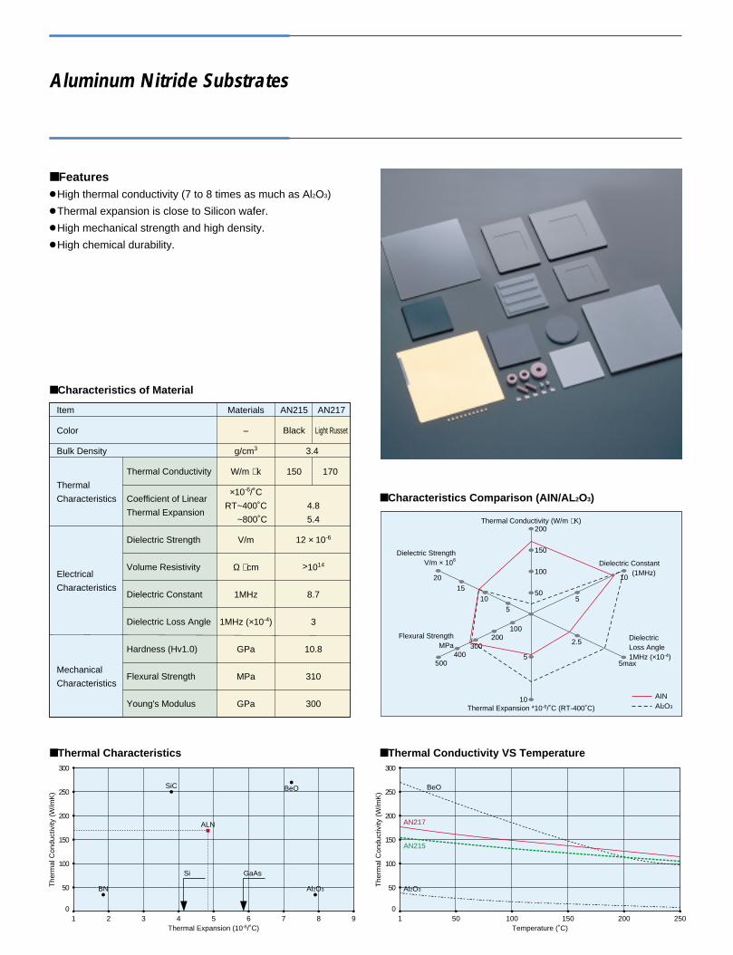
Aluminum Nitride Substrates
Features High thermal conductivity (7 to 8 times as much as Al2O3) Thermal expansion is close to Silicon wafer. High mechanical strength and high density. High chemical durability.
Characteristics of Material
Thermal Characteristics Thermal Conductivity VS Temperature
Characteristics Comparison (AIN/AL2O3)
Item Materials AN215 AN217
Color – Black Light Russet
Bulk Density g/cm3 3.4
W/m ⋅ k 150 170Thermal Conductivity
Thermal×10-6/˚C
Characteristics Coefficient of LinearRT~400˚C 4.8
Thermal Expansion ~800˚C 5.4
V/m 12 × 10-6Dielectric Strength
Ω ⋅ cm >1014
ElectricalVolume Resistivity
Characteristics1MHz 8.7Dielectric Constant
1MHz (×10-4) 3Dielectric Loss Angle
GPa 10.8Hardness (Hv1.0)
MechanicalMPa 310
CharacteristicsFlexural Strength
GPa 300Young's Modulus
0
50
100
150
200
250
300
1
SiC
ALN
BeO
2 3 4 5 6 7 8 9
BN
Si
Al2O3
GaAs
Thermal Expansion (10-6/˚C)
The
rmal
Con
duct
ivity
(W
/mK
)
0
50
100
150
200
250
300
1 50 100 150 200 250
BeO
AN217
AN215
Temperature (˚C)
The
rmal
Con
duct
ivity
(W
/mK
)
Al2O3
50
100
55
10
10
15
20
200300
400500
5
2.5
5max
AIN10
100
150
200Thermal Conductivity (W/m ⋅ K)
Thermal Expansion *10-6/˚C (RT-400˚C)
Dielectric StrengthV/m × 106
Flexural StrengthMPa
DielectricLoss Angle1MHz (×10-4)
Dielectric Constant(1MHz)
Al2O3
Multiform Glass
Features High thermal resistivity High mechanical strength Excellent dielectric strength High electrical resistivity Sealing operation is made simple
Characteristics of Material
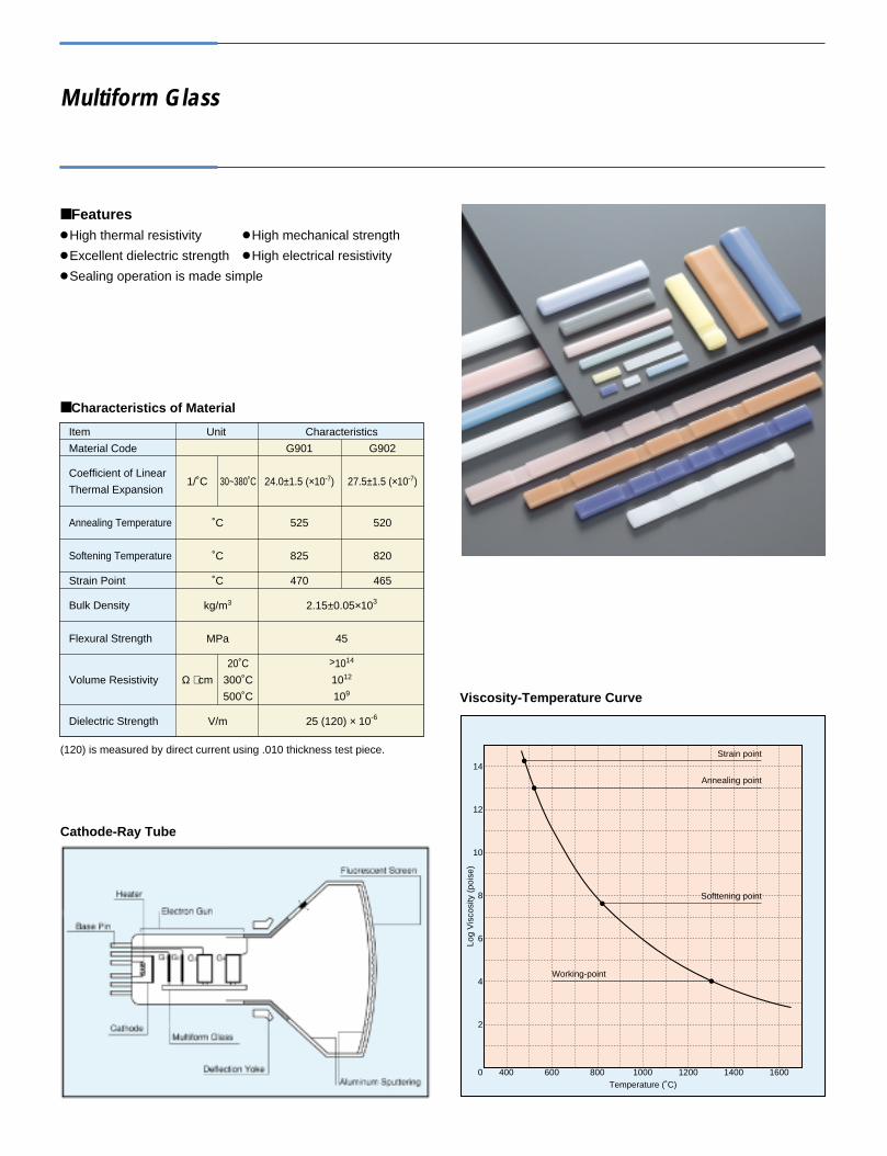
Cathode-Ray Tube
Viscosity-Temperature Curve
Item Unit Characteristics
Material Code G901 G902
Coefficient of Linear1/˚C 30~380˚C 24.0±1.5 (×10-7) 27.5±1.5 (×10-7)
Thermal Expansion
˚C 525 520Annealing Temperature
˚C 825 820Softening Temperature
Strain Point ˚C 470 465
kg/m3 2.15±0.05×10³Bulk Density
MPa 45Flexural Strength
20˚C >1014
Volume Resistivity Ω ⋅ cm 300˚C 1012
500˚C 109
V/m 25 (120) × 10-6Dielectric Strength
(120) is measured by direct current using .010 thickness test piece.
0
2
4
6
8
10
12
14
400 600 800 1000 1200 1400 1600
Strain point
Annealing point
Softtening point
Working-point
Temperature (˚C)
Log
Vis
cosi
ty (
pois
e)
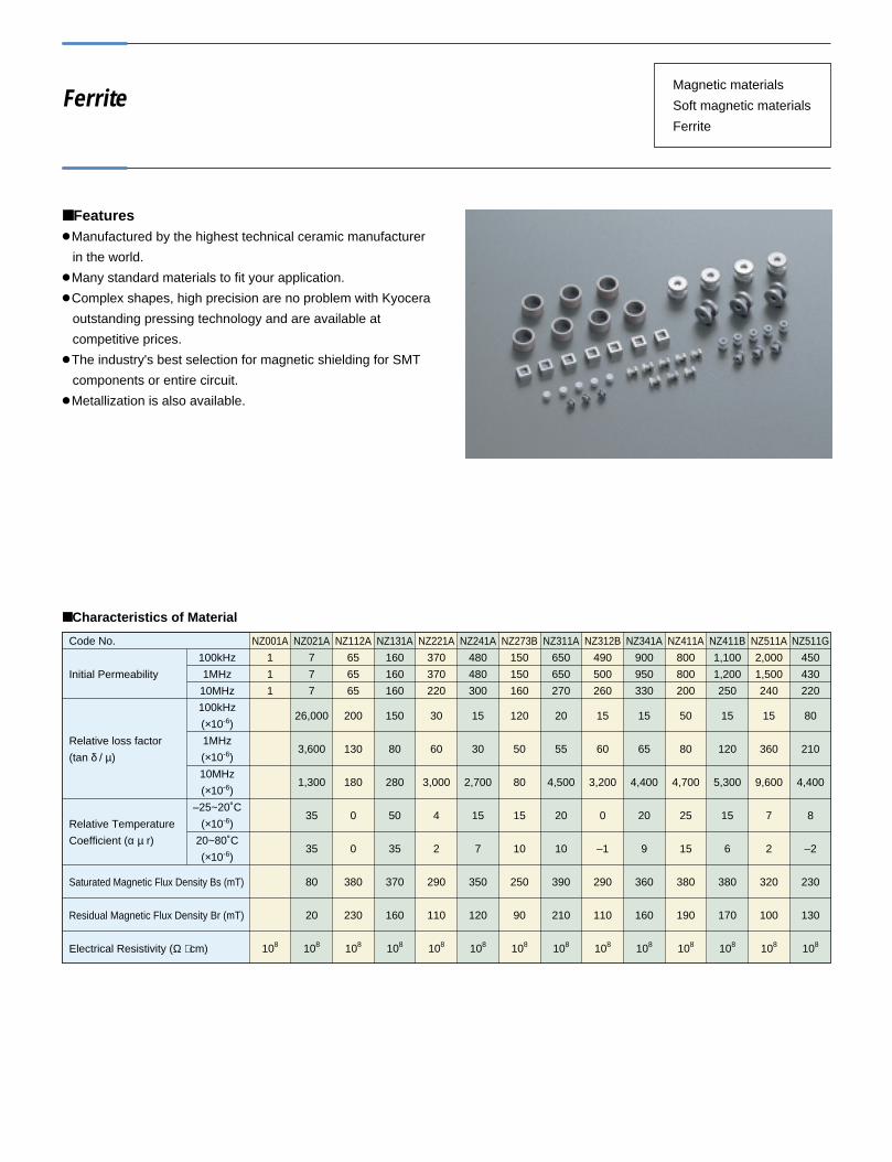
Ferrite
Features Manufactured by the highest technical ceramic manufacturer
in the world. Many standard materials to fit your application. Complex shapes, high precision are no problem with Kyocera
outstanding pressing technology and are available at
competitive prices. The industry's best selection for magnetic shielding for SMT
components or entire circuit. Metallization is also available.
Characteristics of Material
Magnetic materials
Soft magnetic materials
Ferrite
Code No.
Initial Permeability
Relative loss factor
(tan δ / µ)
Relative Temperature
Coefficient (α µ r)
Saturated Magnetic Flux Density Bs (mT)
Residual Magnetic Flux Density Br (mT)
Electrical Resistivity (Ω ⋅ cm)
100kHz
1MHz
10MHz
100kHz
(×10-6)
1MHz
(×10-6)
10MHz
(×10-6)
–25~20˚C
(×10-6)
20~80˚C
(×10-6)
NZ001A
1
1
1
108
NZ021A
7
7
7
26,000
3,600
1,300
35
35
80
20
108
NZ112A
65
65
65
200
130
180
0
0
380
230
108
NZ131A
160
160
160
150
80
280
50
35
370
160
108
NZ221A
370
370
220
30
60
3,000
4
2
290
110
108
NZ241A
480
480
300
15
30
2,700
15
7
350
120
108
NZ273B
150
150
160
120
50
80
15
10
250
90
108
NZ311A
650
650
270
20
55
4,500
20
10
390
210
108
NZ312B
490
500
260
15
60
3,200
0
–1
290
110
108
NZ341A
900
950
330
15
65
4,400
20
9
360
160
108
NZ411A
800
800
200
50
80
4,700
25
15
380
190
108
NZ411B
1,100
1,200
250
15
120
5,300
15
6
380
170
108
NZ511A
2,000
1,500
240
15
360
9,600
7
2
320
100
108
NZ511G
450
430
220
80
210
4,400
8
–2
230
130
108
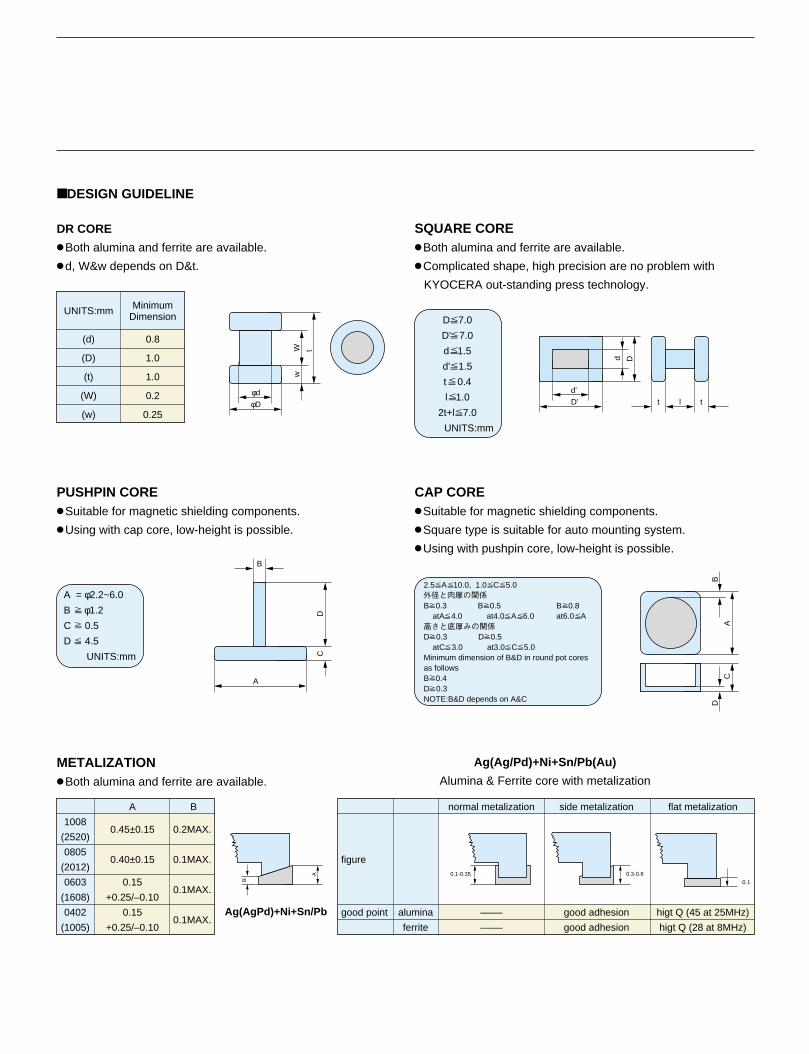
DESIGN GUIDELINE
DR CORE Both alumina and ferrite are available. d, W&w depends on D&t.
SQUARE CORE Both alumina and ferrite are available. Complicated shape, high precision are no problem with
KYOCERA out-standing press technology.
PUSHPIN CORE Suitable for magnetic shielding components. Using with cap core, low-height is possible.
METALIZATION Both alumina and ferrite are available.
CAP CORE Suitable for magnetic shielding components. Square type is suitable for auto mounting system. Using with pushpin core, low-height is possible.
Ag(Ag/Pd)+Ni+Sn/Pb(Au)
Alumina & Ferrite core with metalization
Ag(AgPd)+Ni+Sn/Pb
UNITS:mm
(d)
(D)
(t)
(W)
(w)
MinimumDimension
0.8
1.0
1.0
0.2
0.25
φd
φD
Ww
t
D 7.0
D' 7.0
d 1.5
d' 1.5
t 0.4
l 1.0
2t+l 7.0
UNITS:mm
2.5 A 10.0, 1.0 C 5.0
B 0.3 B 0.5 B 0.8 atA 4.0 at4.0 A 6.0 at6.0 A
D 0.3 D 0.5 atC 3.0 at3.0 C 5.0Minimum dimension of B&D in round pot cores as followsB 0.4D 0.3NOTE:B&D depends on A&C
A = φ2.2~6.0
B φ1.2
C 0.5
D 4.5
UNITS:mm
D' lt t
d'
d D
A
DC
B
BD
AC
A B
10080.45±0.15 0.2MAX.
(2520)
08050.40±0.15 0.1MAX.
(2012)
0603 0.150.1MAX.
(1608) +0.25/–0.10
0402 0.150.1MAX.
(1005) +0.25/–0.10
normal metalization side metalization flat metalization
figure
good point alumina –––– good adhesion higt Q (45 at 25MHz)
ferrite –––– good adhesion higt Q (28 at 8MHz)
0.1
0.3-0.80.1-0.35A
B
Single Crystal Sapphire Substrates
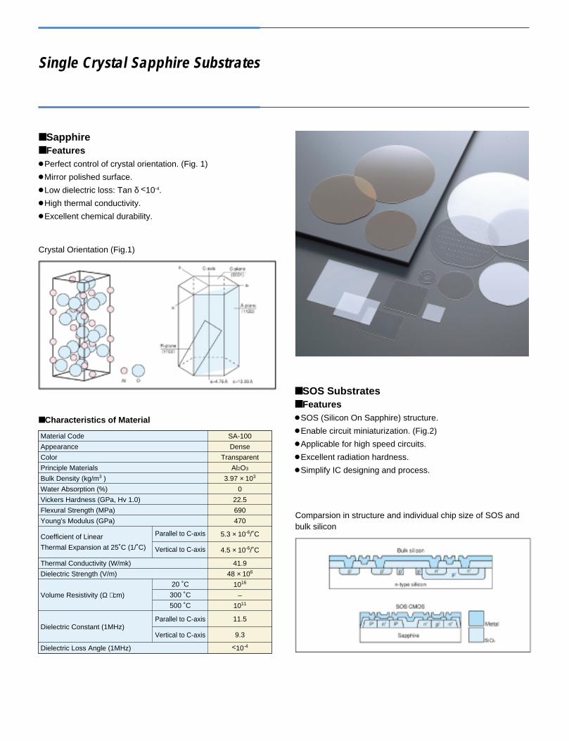
Sapphire Features Perfect control of crystal orientation. (Fig. 1) Mirror polished surface. Low dielectric loss: Tan δ <10-4. High thermal conductivity. Excellent chemical durability.
SOS Substrates Features SOS (Silicon On Sapphire) structure. Enable circuit miniaturization. (Fig.2) Applicable for high speed circuits. Excellent radiation hardness. Simplify IC designing and process.
Crystal Orientation (Fig.1)
Characteristics of Material
Comparsion in structure and individual chip size of SOS and bulk silicon
Material Code
Appearance
Color
Principle Materials
Bulk Density (kg/m3 )
Water Absorption (%)
Vickers Hardness (GPa, Hv 1.0)
Flexural Strength (MPa)
Young's Modulus (GPa)
Coefficient of Linear
Thermal Expansion at 25˚C (1/˚C)
Thermal Conductivity (W/mk)
Dielectric Strength (V/m)
Volume Resistivity (Ω ⋅ cm)
Dielectric Constant (1MHz)
Dielectric Loss Angle (1MHz)
Parallel to C-axis
Vertical to C-axis
20 ˚C
300 ˚C
500 ˚C
Parallel to C-axis
Vertical to C-axis
SA-100
Dense
Transparent
Al2O3
3.97 × 10³
0
22.5
690
470
5.3 × 10⁻⁶/˚C
4.5 × 10⁻⁶/˚C
41.9
48 × 106
1016
–
1011
11.5
9.3
<10-4
Recommended