Carrier Concentrations
Presented by Chanam Lee
August 22nd
Carrier Concentration
� Carrier Properties
� State and Carrier Distributions
� Equilibrium Carrier Concentration
� Carrier Concentration for the Quantum Well Devices
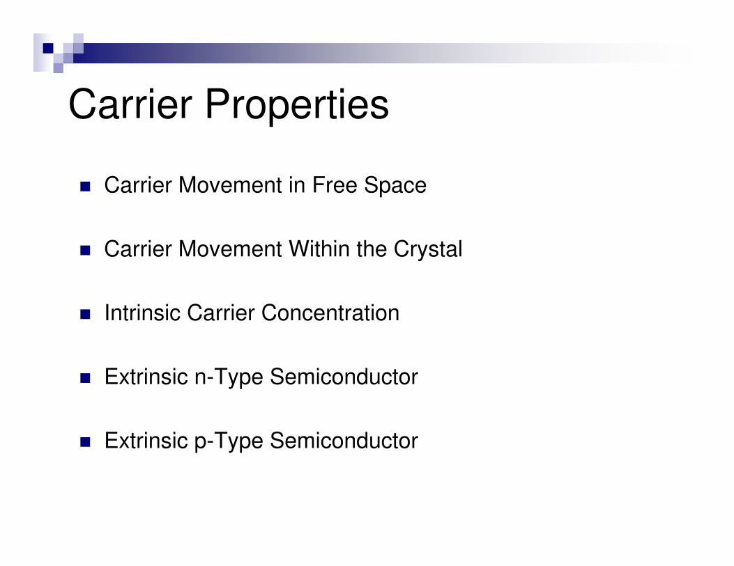
Carrier Properties
� Carrier Movement in Free Space
� Carrier Movement Within the Crystal
� Intrinsic Carrier Concentration
� Extrinsic n-Type Semiconductor
� Extrinsic p-Type Semiconductor
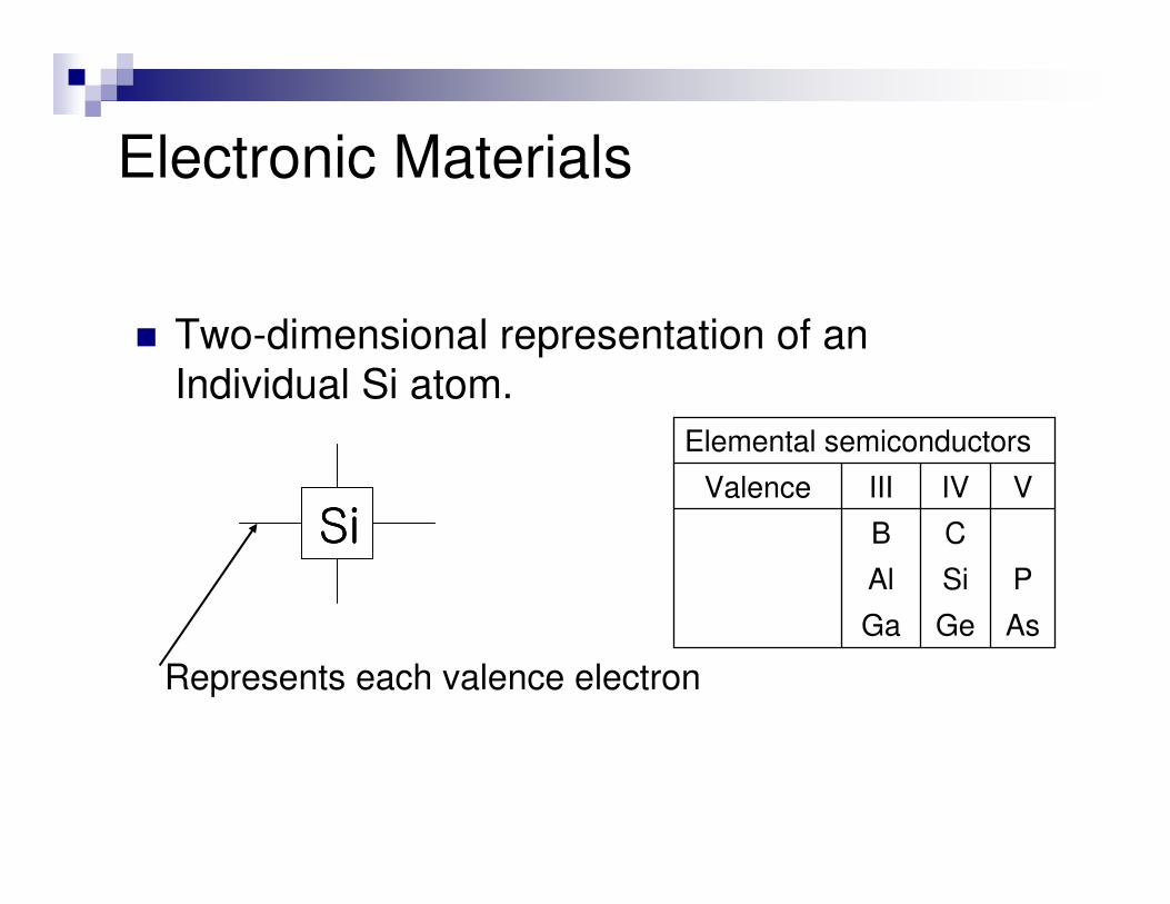
Electronic Materials
� Two-dimensional representation of an Individual Si atom.
Represents each valence electronAsGeGa
PSiAl
CB
VIVIIIValence
Elemental semiconductors
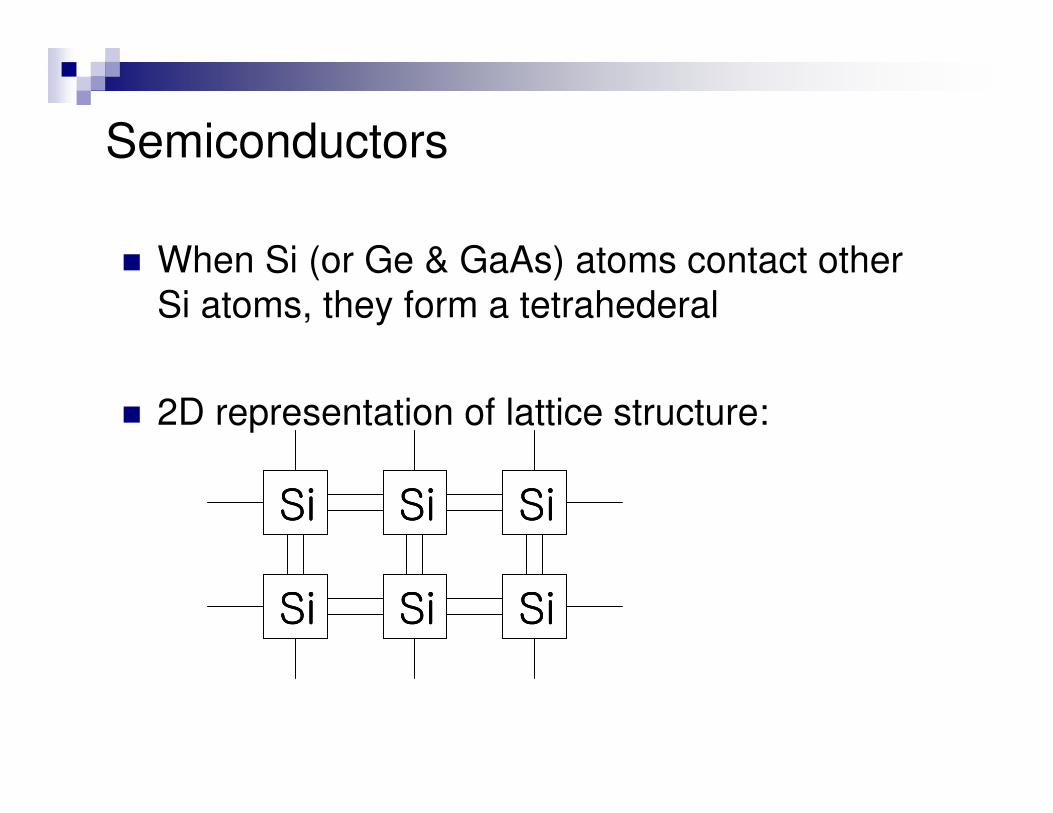
Semiconductors
� When Si (or Ge & GaAs) atoms contact other Si atoms, they form a tetrahederal
� 2D representation of lattice structure:
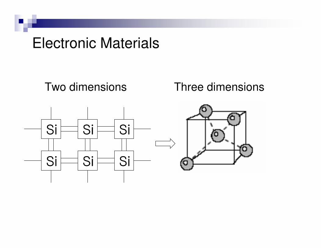
Electronic Materials
Two dimensions Three dimensions
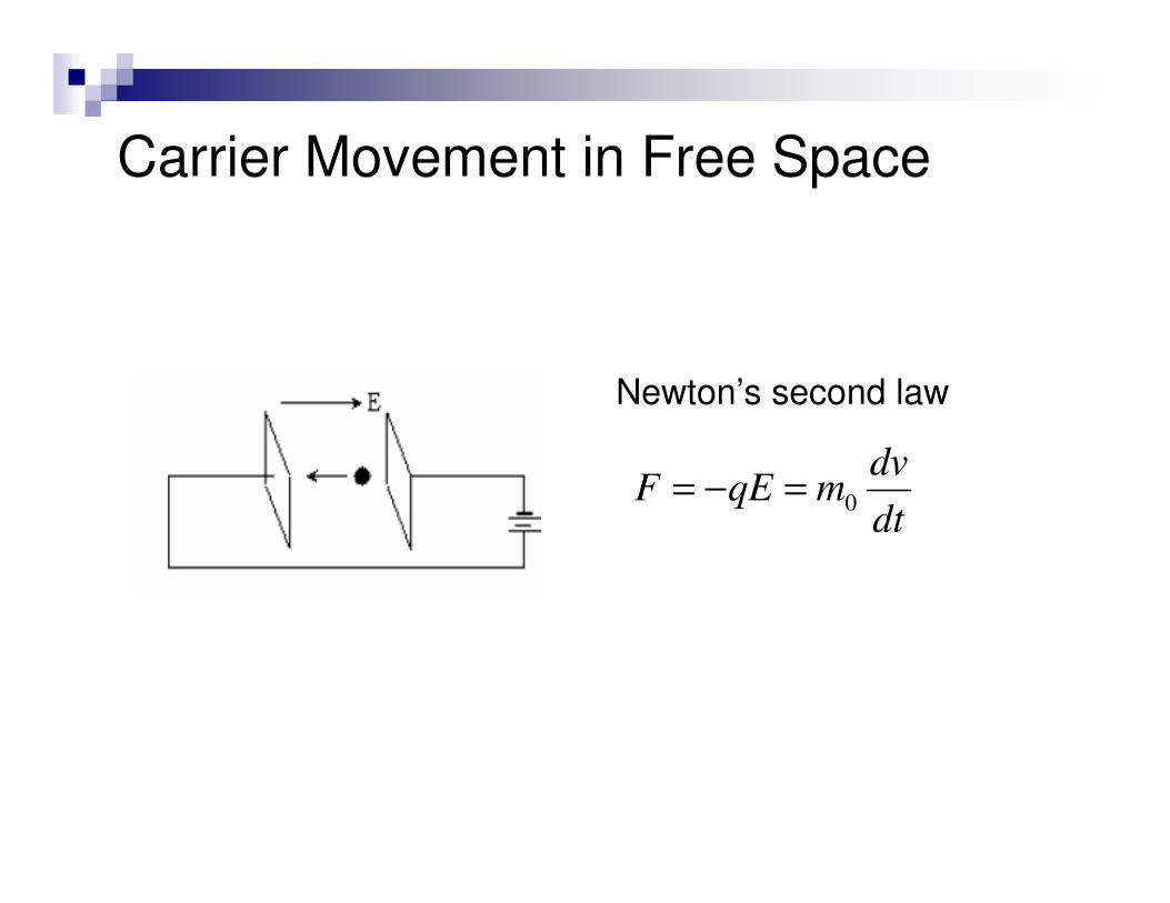
Carrier Movement in Free Space
Newton’s second law
dtdv
mqEF 0=−=
Carrier Movement Within the Crystal
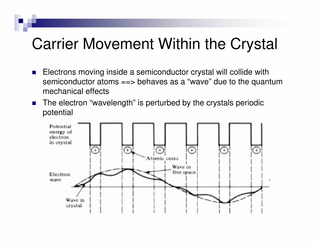
� Electrons moving inside a semiconductor crystal will collide with semiconductor atoms ==> behaves as a “wave” due to the quantum mechanical effects
� The electron “wavelength” is perturbed by the crystals periodic potential
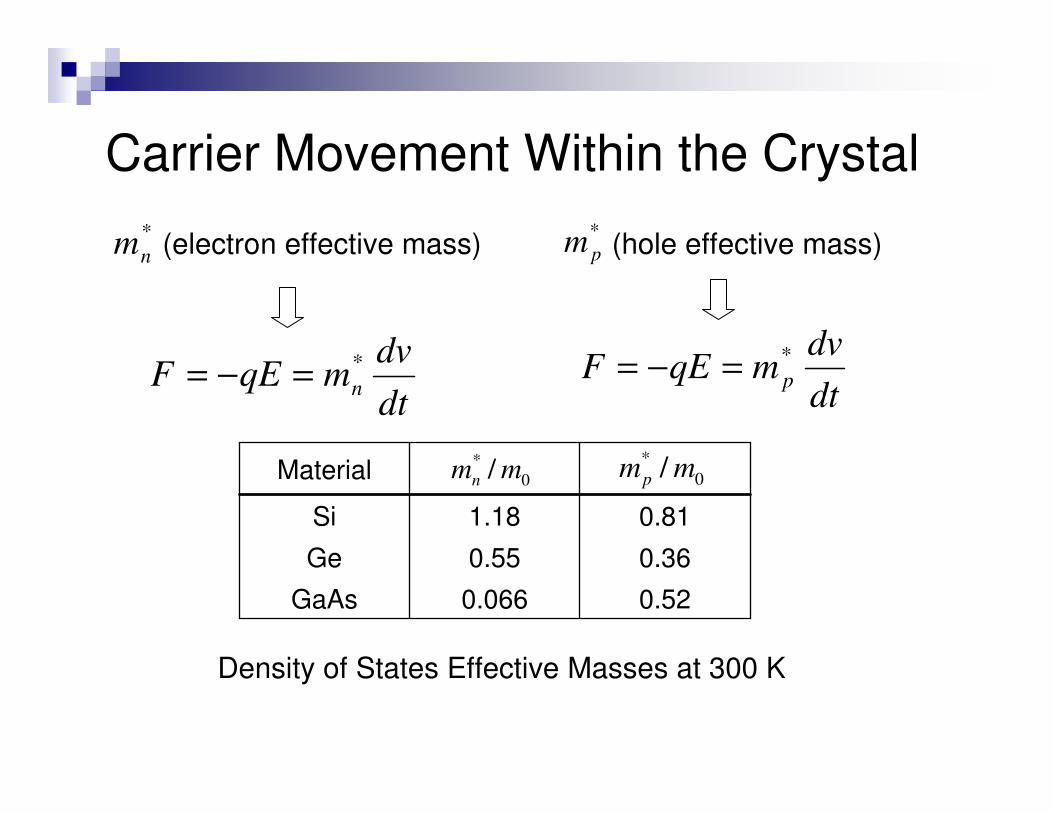
Carrier Movement Within the Crystal
(electron effective mass) (hole effective mass)
Density of States Effective Masses at 300 K
0.520.066GaAs
0.360.55Ge
0.811.18Si
Material
dtdv
mqEF n*=−=
*nm
dtdv
mqEF p*=−=
*pm
0* / mmp0
* / mmn
Intrinsic Carrier Concentration
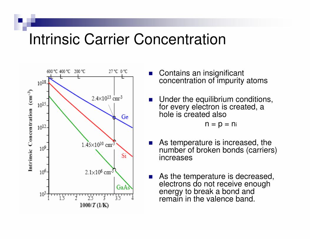
� Contains an insignificant concentration of impurity atoms
� Under the equilibrium conditions, for every electron is created, a hole is created also
n = p = ni
� As temperature is increased, the number of broken bonds (carriers) increases
� As the temperature is decreased, electrons do not receive enough energy to break a bond and remain in the valence band.
Extrinsic n-Type Semiconductor
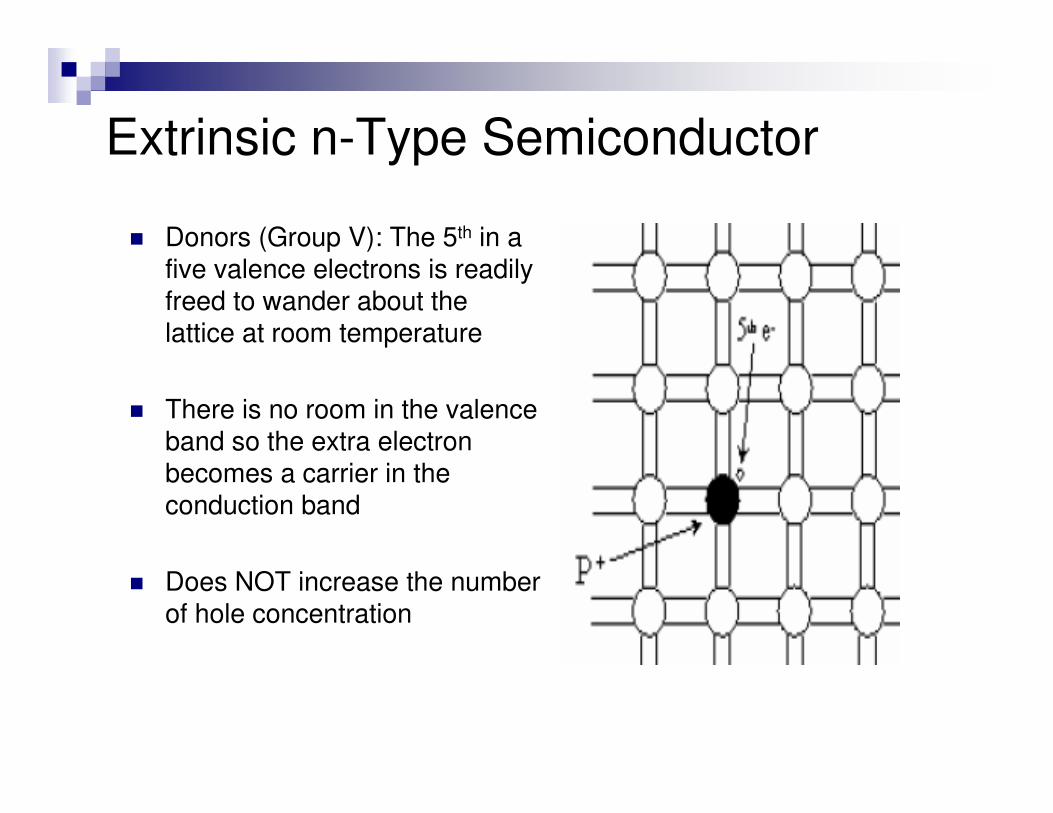
� Donors (Group V): The 5th in a five valence electrons is readily freed to wander about the lattice at room temperature
� There is no room in the valence band so the extra electron becomes a carrier in the conduction band
� Does NOT increase the number of hole concentration
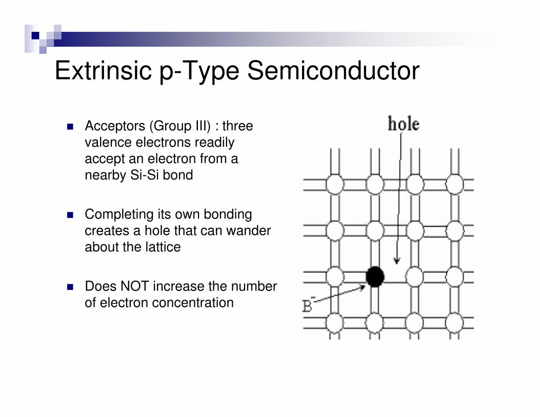
Extrinsic p-Type Semiconductor
� Acceptors (Group III) : three valence electrons readily accept an electron from a nearby Si-Si bond
� Completing its own bonding creates a hole that can wander about the lattice
� Does NOT increase the number of electron concentration
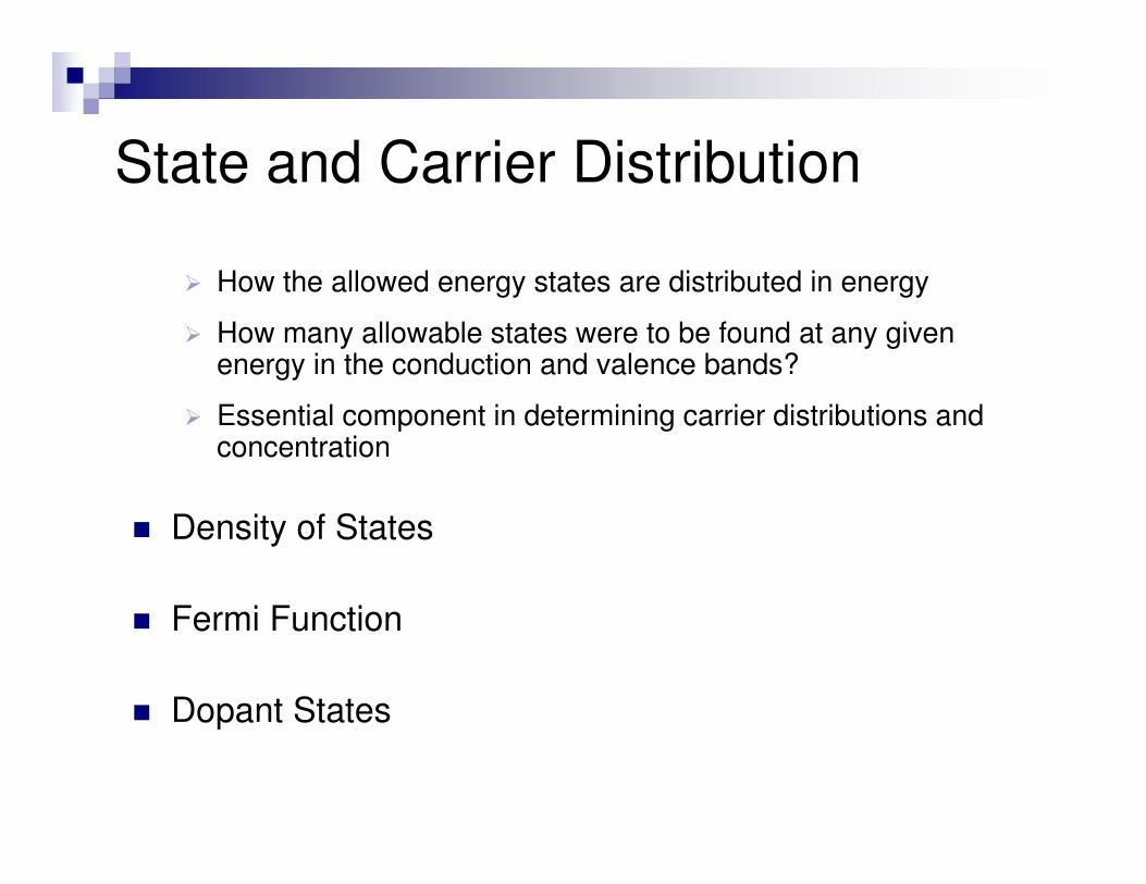
State and Carrier Distribution
� How the allowed energy states are distributed in energy
� How many allowable states were to be found at any given energy in the conduction and valence bands?
� Essential component in determining carrier distributions and concentration
� Density of States
� Fermi Function
� Dopant States
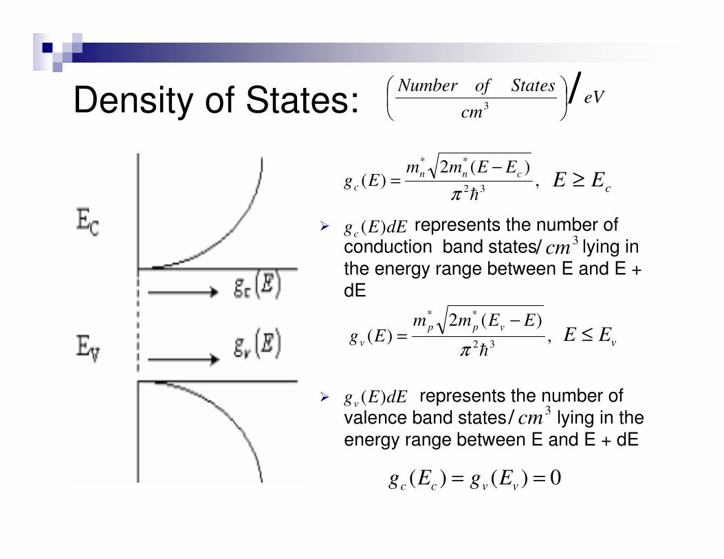
Density of States:
� represents the number of conduction band states lying in the energy range between E and E + dE
� represents the number of valence band states lying in the energy range between E and E + dE
,)(2
)( 32
**
�πcnn
c
EEmmEg
−= cEE ≥
,)(2
)( 32
**
�πEEmm
Egvpp
v
−= vEE ≤
0)()( == vvcc EgEg
dEEgc )(
dEEgv )(
3/ cm
3/ cm
eVcm
StatesofNumber /3 ��
���
�
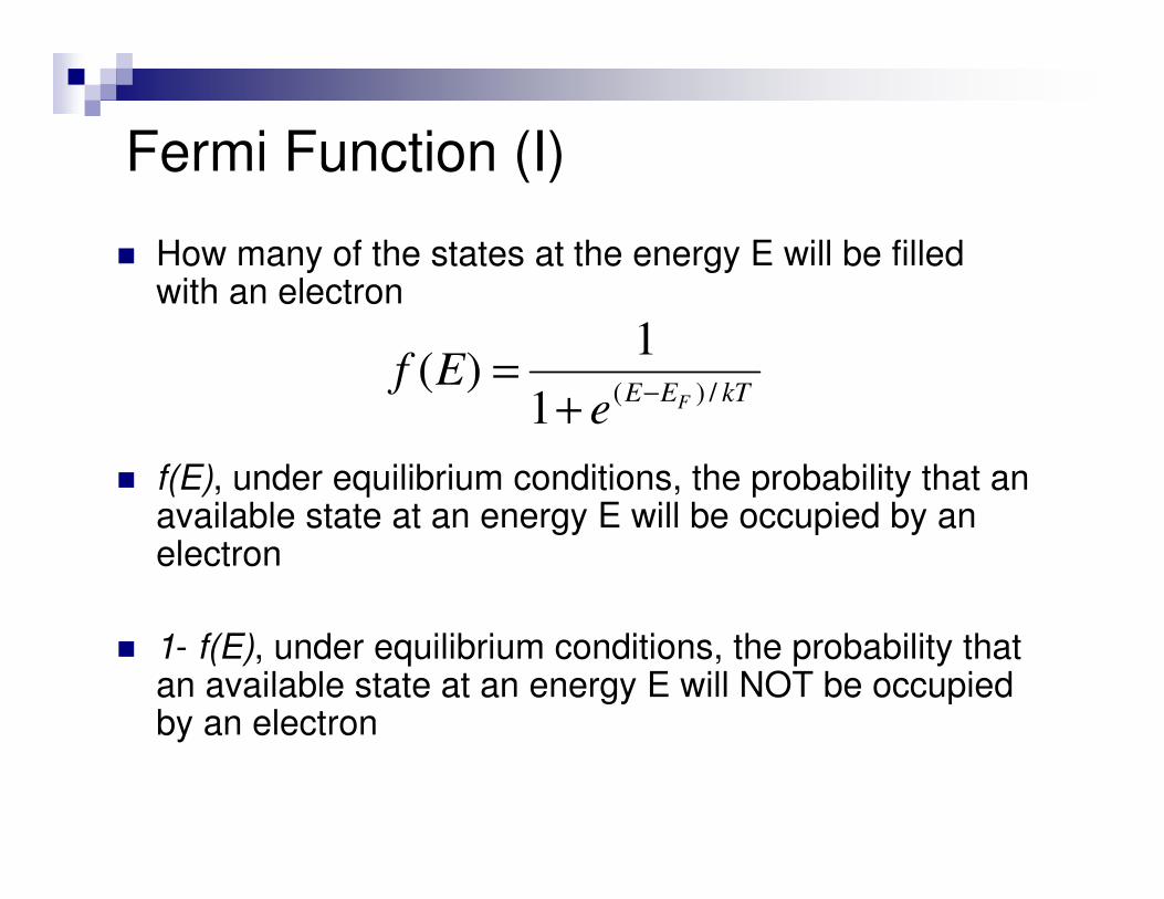
Fermi Function (I)
� How many of the states at the energy E will be filled with an electron
� f(E), under equilibrium conditions, the probability that an available state at an energy E will be occupied by an electron
� 1- f(E), under equilibrium conditions, the probability that an available state at an energy E will NOT be occupied by an electron
kTEE FeEf /)(1
1)( −+
=
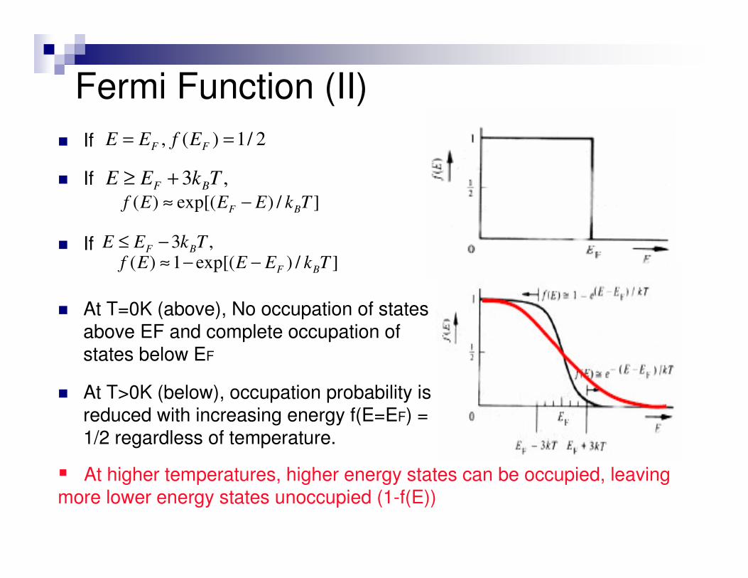
Fermi Function (II)� If
� If
� If
� At T=0K (above), No occupation of states above EF and complete occupation of states below EF
� At T>0K (below), occupation probability is reduced with increasing energy f(E=EF) = 1/2 regardless of temperature.
2/1)(, == FF EfEE
,3 TkEE BF +≥]/)exp[()( TkEEEf BF −≈
,3 TkEE BF −≤]/)exp[(1)( TkEEEf BF−−≈
� At higher temperatures, higher energy states can be occupied, leaving more lower energy states unoccupied (1-f(E))
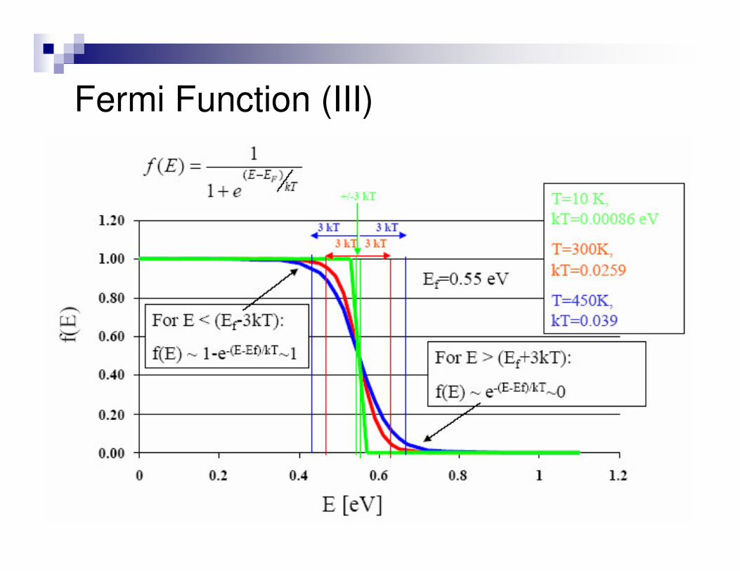
Fermi Function (III)
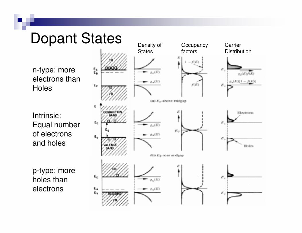
Dopant States
n-type: moreelectrons thanHoles
Intrinsic:Equal numberof electronsand holes
p-type: moreholes thanelectrons
Density of States
Occupancy factors
Carrier Distribution
Equilibrium Carrier Concentration
� Formulas for n and p
� Degenerate vs. Non-degenerate Semiconductor
� Alternative Expressions for n and p
� ni and the np Product
� Charge Neutrality Relationship
� Carrier Concentration Calculations
� Determination of EF
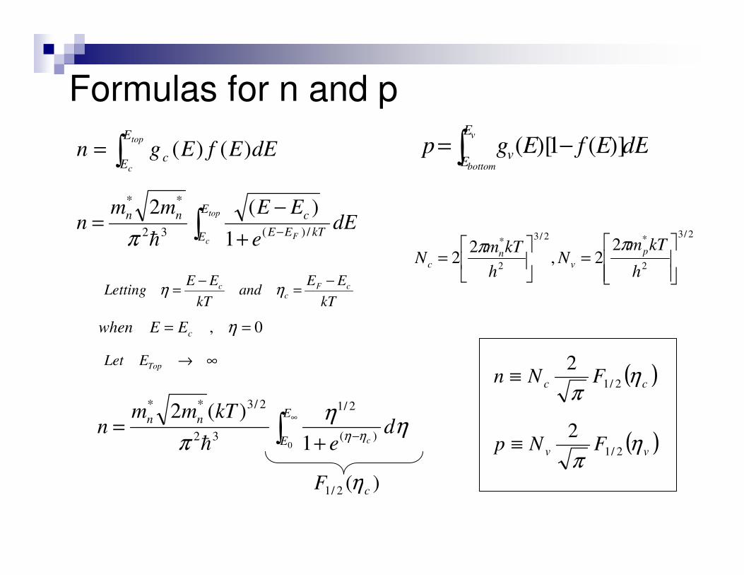
Formulas for n and p
�= top
c
E
E c dEEfEgn )()(
� −+−
= top
c F
E
E kTEEcnn dE
e
EEmmn /)(32
**
1)(2
�π
kTEE
andkT
EELetting cF
cc −=−= ηη
0, == ηcEEwhen
∞→TopELet
�∞
−+=
E
E
nn de
kTmmn
c0)(
2/1
32
2/3**
1)(2
ηηπ ηη
�
)(2/1 cF η
2/3
2
*2/3
2
* 22,
22
��
���
=�
��
=
h
kTmN
hkTm
N pv
nc
ππ
( )cc FNn ηπ 2/1
2≡
� −= v
bottom
E
E v dEEfEgp )](1)[(
( )vv FNp ηπ 2/1
2≡
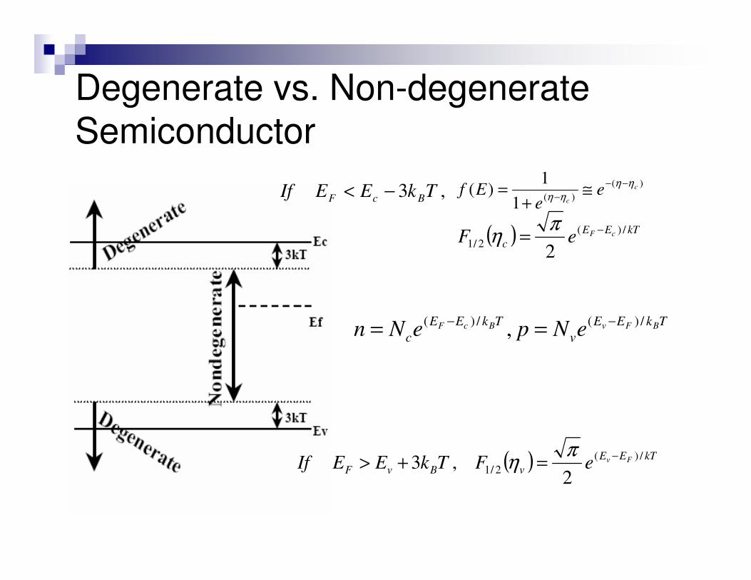
Degenerate vs. Non-degenerate Semiconductor
( ) kTEEc
cFeF /)(2/1 2
−= πη
TkEEv
TkEEc
BFvBcF eNpeNn /)(/)( , −− ==
,3 TkEEIf BcF −< )()(1
1)( c
ce
eEf ηη
ηη−−
− ≅+
=
( ) kTEEv
FveF /)(2/1 2
−= πη,3 TkEEIf BvF +>
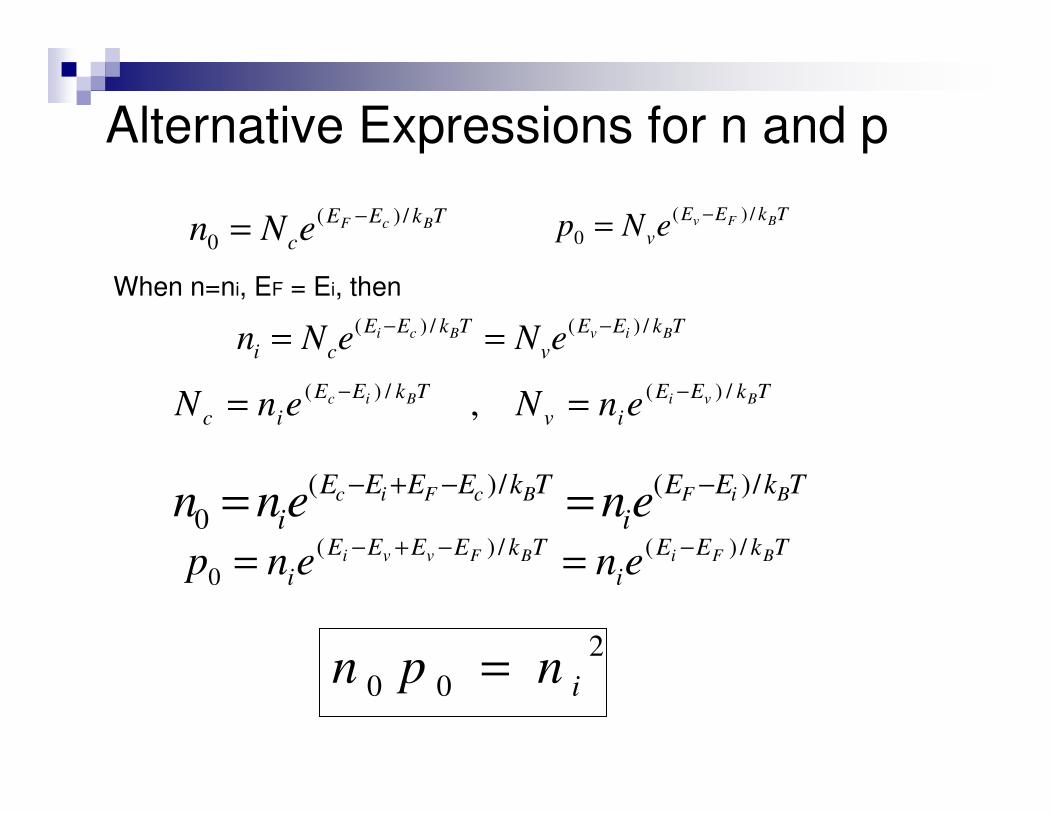
Alternative Expressions for n and p
When n=ni, EF = Ei, thenTkEE
vTkEE
ciBivBci eNeNn /)(/)( −− ==
TkEEc
BcFeNn /)(0
−= TkEEv
BFveNp /)(0
−=
TkEEi
TkEEEEi
BiFBcFic enenn /)(/)(0
−−+− ==TkEE
iTkEEEE
iBFiBFvvi enenp /)(/)(
0−−+− ==
200 inpn =
TkEEiv
TkEEic
BviBic enNenN /)(/)( , −− ==
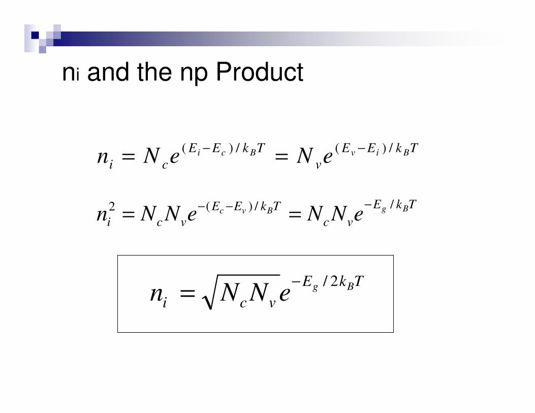
ni and the np Product
TkEvc
TkEEvci
BgBvc eNNeNNn //)(2 −−− ==
TkEEv
TkEEci
BivBci eNeNn /)(/)( −− ==
TkEvci
BgeNNn 2/−=
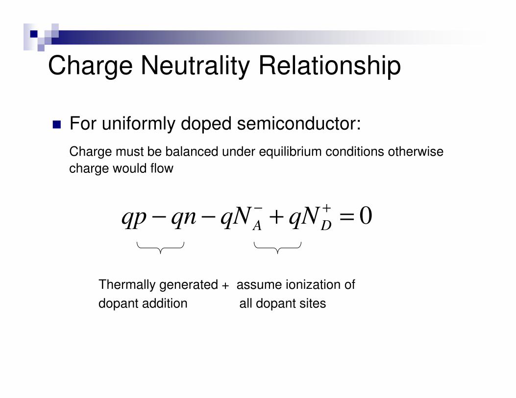
Charge Neutrality Relationship
� For uniformly doped semiconductor:Charge must be balanced under equilibrium conditions otherwise charge would flow
Thermally generated + assume ionization of dopant addition all dopant sites
0=+−− +−DA qNqNqnqp
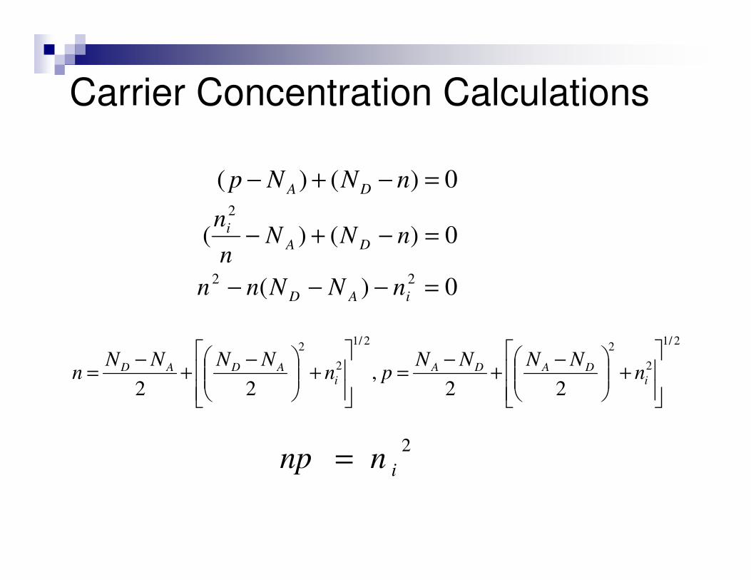
Carrier Concentration Calculations
0)()( =−+− nNNp DA
2/1
2
22/1
2
2
22,
22 ��
��
�
+��
�
����
� −+−=��
��
�
+��
�
����
� −+−= iDADA
iADAD n
NNNNpn
NNNNn
2innp =
0)()(2
=−+− nNNn
nDA
i
0)( 22 =−−− iAD nNNnn
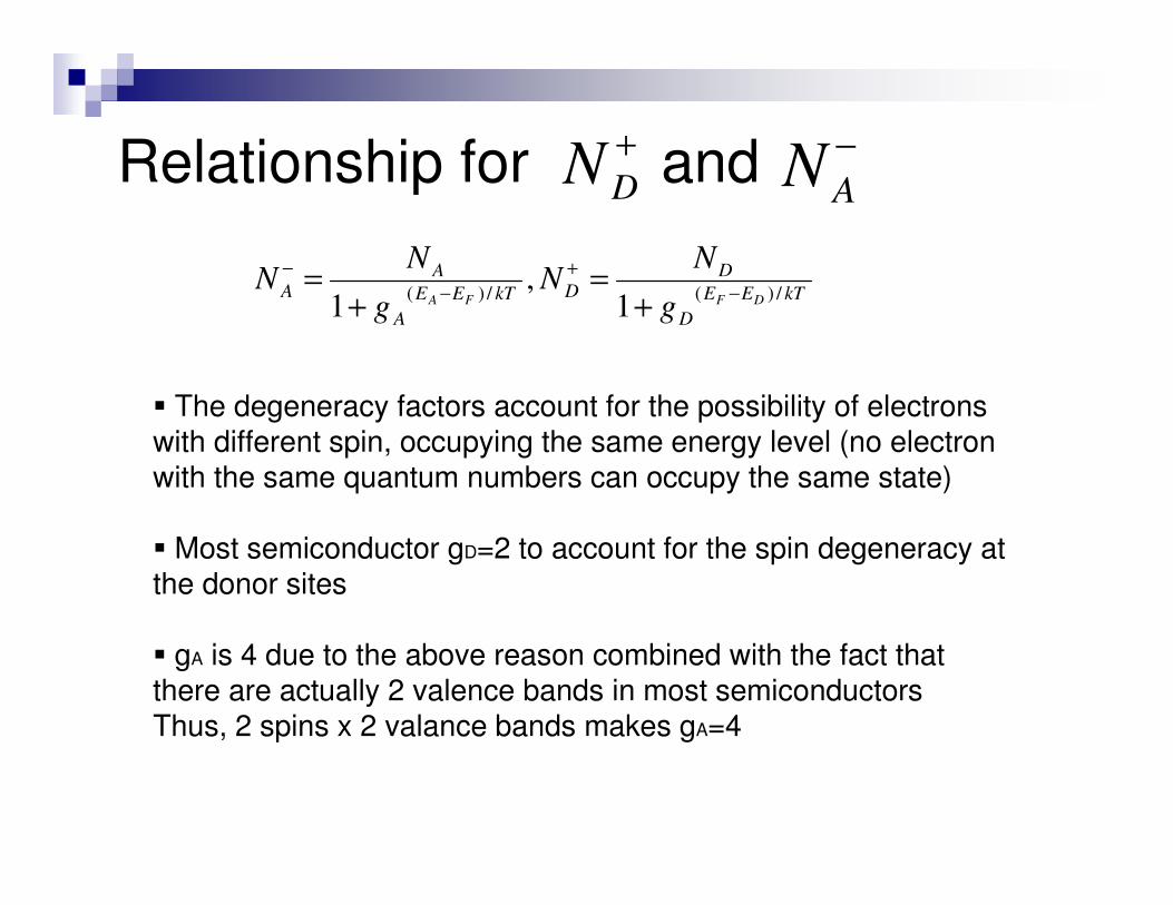
Relationship for and +DN −
AN
kTEED
DDkTEE
A
AA DFFA g
NN
gN
N /)(/)( 1,
1 −+
−−
+=
+=
� The degeneracy factors account for the possibility of electronswith different spin, occupying the same energy level (no electron with the same quantum numbers can occupy the same state)
� Most semiconductor gD=2 to account for the spin degeneracy at the donor sites
� gA is 4 due to the above reason combined with the fact thatthere are actually 2 valence bands in most semiconductorsThus, 2 spins x 2 valance bands makes gA=4
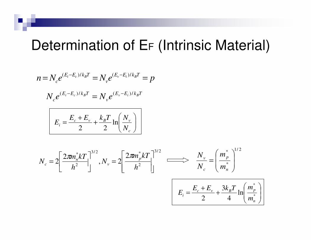
Determination of EF (Intrinsic Material)
TkEEv
TkEEc
BivBci eNeN /)(/)( −− =
peNeNn TkEEv
TkEEc
BivBci === −− /)(/)(
2/3
2
*2/3
2
* 22,
22
��
���
=�
��
=
h
kTmN
hkTm
N pv
nc
ππ
���
����
�++=
c
vBvci N
NTkEEE ln
22
��
�
�
��
�
�++= *
*
ln4
32 n
pBvci m
mTkEEE
2/1
*
*
��
�
�
��
�
�=
n
p
c
v
m
m
NN
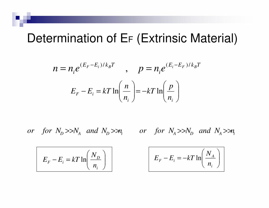
Determination of EF (Extrinsic Material)
���
����
�=−
i
DiF n
NkTEE ln
���
����
�−=��
�
����
�=−
iiiF n
pkT
nn
kTEE lnln
���
����
�−=−
i
AiF n
NkTEE ln
iDAD nNandNNforor >>>> iADA nNandNNforor >>>>
TkEEi
TkEEi
BFiBiF enpenn /)(/)( , −− ==
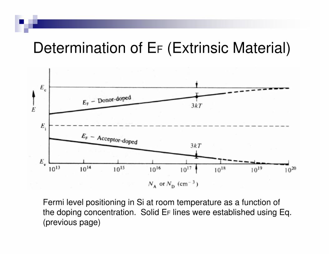
Determination of EF (Extrinsic Material)
Fermi level positioning in Si at room temperature as a function of the doping concentration. Solid EF lines were established using Eq. (previous page)
Carrier Concentration for the Quantum Well Devices
� Density of States 3D vs. 2D
� Carrier Concentration – 2D
� Charge Neutrality
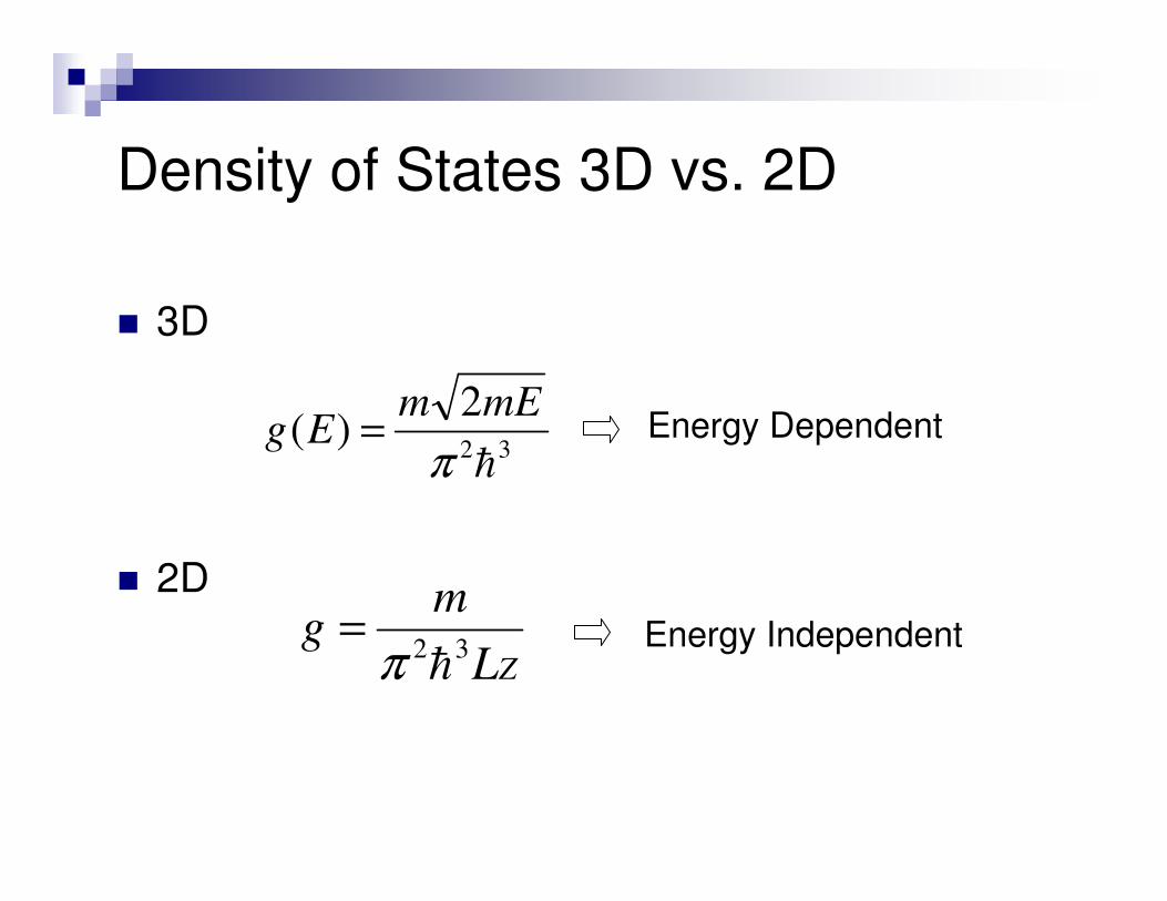
Density of States 3D vs. 2D
32
2)(
�πmEm
Eg =
� 3D
Energy Dependent
� 2DEnergy Independent
ZLm
g 32�π
=
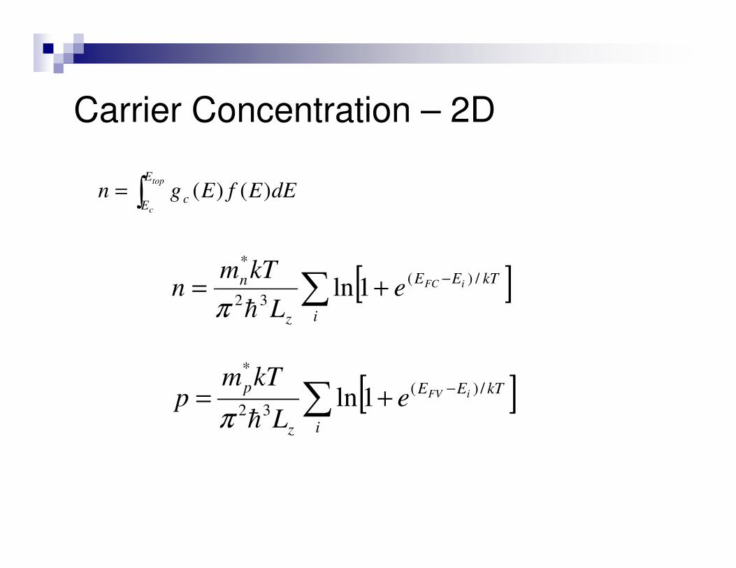
Carrier Concentration – 2D
[ ]� −+=i
kTEE
z
n iFCeL
kTmn /)(
32
*
1ln�π
[ ]� −+=i
kTEE
z
p iFVeL
kTmp /)(
32
*
1ln�π
�= top
c
E
E c dEEfEgn )()(
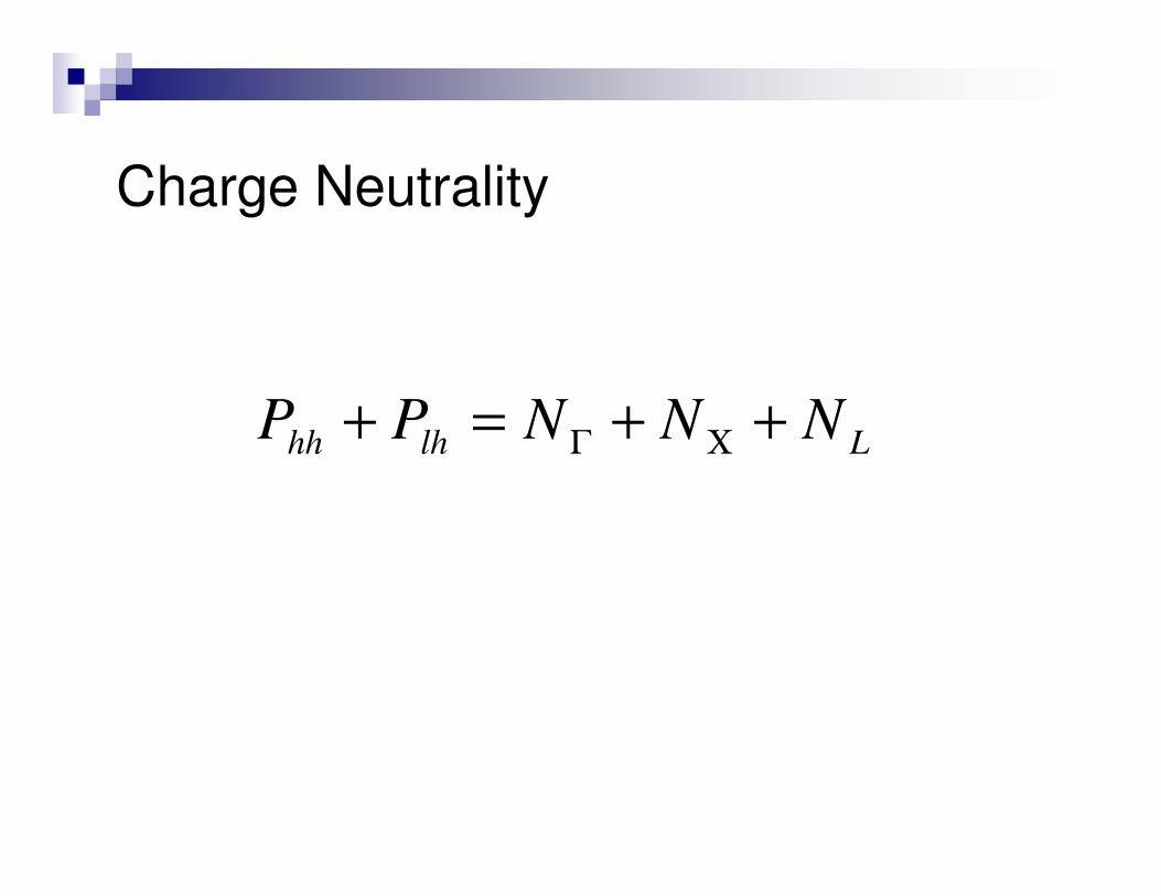
Charge Neutrality
Llhhh NNNPP ++=+ ΧΓ
References
� Robert F. Pierret, Semiconductor Fundamentals (VOLUME I), Addison-Wesley Publishing Company, 1988, chapter 2
� Robert F. Pierret, Advanced Semiconductor Fundamentals (VOLUME VI), Addison-Wesley Publishing Company, 1987, chapter 4
� Ben G. Streetman and Sanjay Banerjee, Solid State Electronic Devices, Prentice Hall, Inc., 2000, chapter 3
� Peter S. Zory, JR., Quantum Well Lasers, Academic Press, 1993, chapter 1, 7
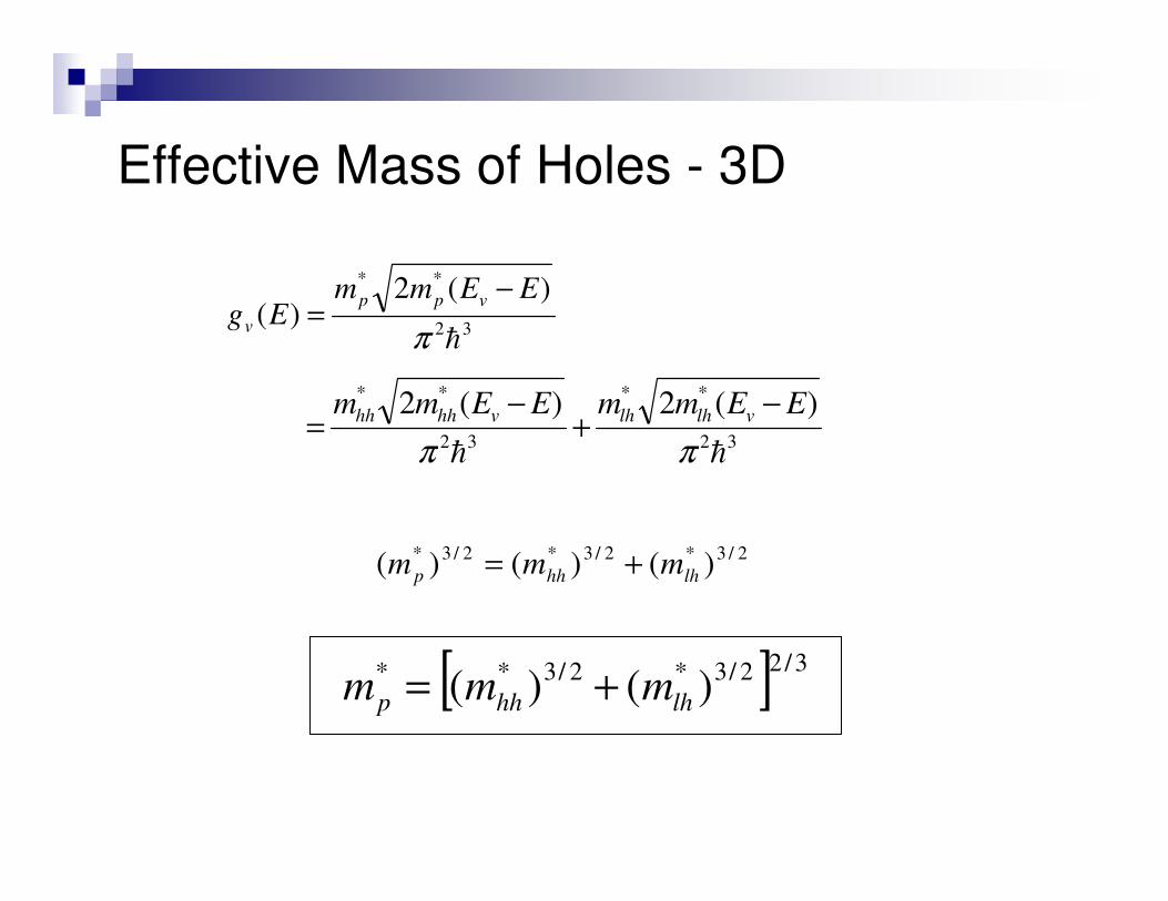
Effective Mass of Holes - 3D
32
**
32
** )(2)(2�� ππ
EEmmEEmm vlhlhvhhhh −+
−=
[ ] 3/22/3*2/3** )()( lhhhp mmm +=
32
** )(2)(
�πEEmm
Eg vppv
−=
2/3*2/3*2/3* )()()( lhhhp mmm +=
Recommended