User’s Manual Page i
USER’S MANUAL VER.1
C10- PARALLEL PORT INTERFACE CARD BOARD Rev. 11
FEBRUARY, 2017
User’s Manual Page ii
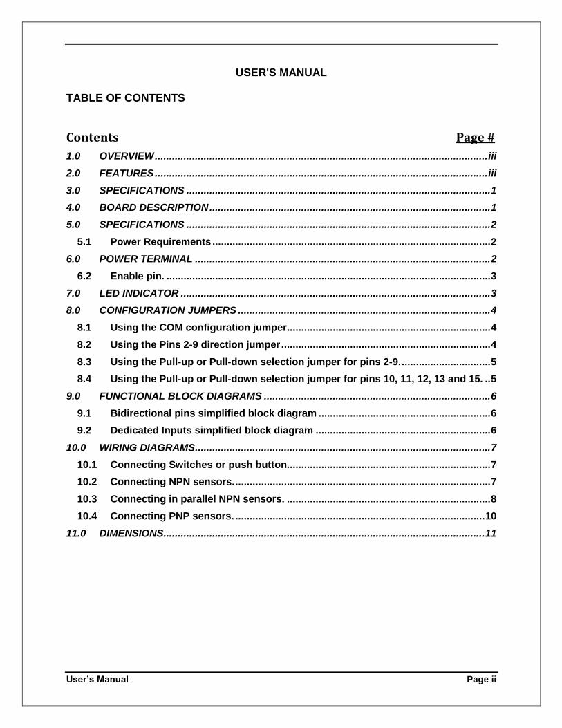
USER'S MANUAL TABLE OF CONTENTS
Contents Page #
1.0 OVERVIEW .................................................................................................................... iii
2.0 FEATURES .................................................................................................................... iii
3.0 SPECIFICATIONS .......................................................................................................... 1
4.0 BOARD DESCRIPTION .................................................................................................. 1
5.0 SPECIFICATIONS .......................................................................................................... 2
5.1 Power Requirements ................................................................................................. 2
6.0 POWER TERMINAL ....................................................................................................... 2
6.2 Enable pin. ................................................................................................................. 3
7.0 LED INDICATOR ............................................................................................................ 3
8.0 CONFIGURATION JUMPERS ........................................................................................ 4
8.1 Using the COM configuration jumper ....................................................................... 4
8.2 Using the Pins 2-9 direction jumper ......................................................................... 4
8.3 Using the Pull-up or Pull-down selection jumper for pins 2-9. ............................... 5
8.4 Using the Pull-up or Pull-down selection jumper for pins 10, 11, 12, 13 and 15. .. 5
9.0 FUNCTIONAL BLOCK DIAGRAMS ............................................................................... 6
9.1 Bidirectional pins simplified block diagram ............................................................ 6
9.2 Dedicated Inputs simplified block diagram ............................................................. 6
10.0 WIRING DIAGRAMS ....................................................................................................... 7
10.1 Connecting Switches or push button. ...................................................................... 7
10.2 Connecting NPN sensors. ......................................................................................... 7
10.3 Connecting in parallel NPN sensors. ....................................................................... 8
10.4 Connecting PNP sensors. ....................................................................................... 10
11.0 DIMENSIONS ................................................................................................................ 11
User’s Manual Page iii
1.0 OVERVIEW
This card provides an easy way of interfacing your inputs and outputs from you parallel port. It provides terminals for the connections and conditions the signals for use in CNC applications.
2.0 FEATURES
IEEE 1284 Standard compatible.
PULL-UP or PULL-DOWN selection for inputs.
Buffered inputs and outputs.
Bidirectional pins 2-9.
Output pins 1, 2, 3, 4, 5, 6, 7, 8, 9, 14, 16, 17. Or 1, 14, 16, 17.
Input pins 10, 11, 12, 13, 15. Or 2, 3, 4, 5, 6, 7, 8, 9, 10, 11, 12, 13, 15.
Input and output pins with close by ground or +5vdc connections .
Input pins 10, 11, 12, 13, 15.
Input and output pins with close by ground or +5vdc connections
External Enable Pin (EN).
Works directly with popular CNC hardware and software.
All TTL 5VDC signals.
Screw-On connections for all terminals.
Status LEDs for enable.
User’s Manual Page 1
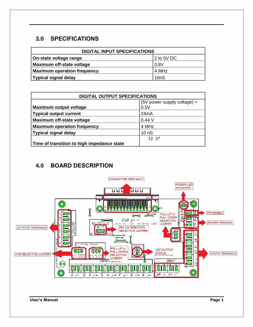
3.0 SPECIFICATIONS
DIGITAL INPUT SPECIFICATIONS
On-state voltage range 2 to 5V DC
Maximum off-state voltage 0.8V
Maximum operation frequency 4 MHz
Typical signal delay 10nS
DIGITAL OUTPUT SPECIFICATIONS
Maximum output voltage (5V power supply voltage) + 0.5V
Typical output current 24mA
Maximum off-state voltage 0.44 V
Maximum operation frequency 4 MHz
Typical signal delay 10 nS
Time of transition to high impedance state 12 S*
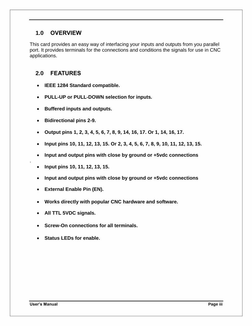
4.0 BOARD DESCRIPTION
User’s Manual Page 2
5.0 SPECIFICATIONS
5.1 Power Requirements
Regulated +5VDC@ 500mA is required to power this board.
WARNING Check the polarity and voltage of the external power source and connect the 5VDC and
GND. Overvoltage or reverse-polarity power applied to these terminals can cause
damage to the board, and/or the power source.
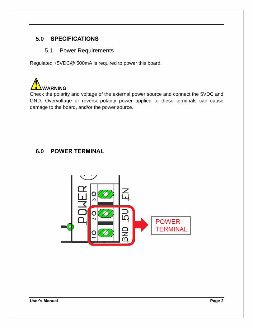
6.0 POWER TERMINAL
User’s Manual Page 3
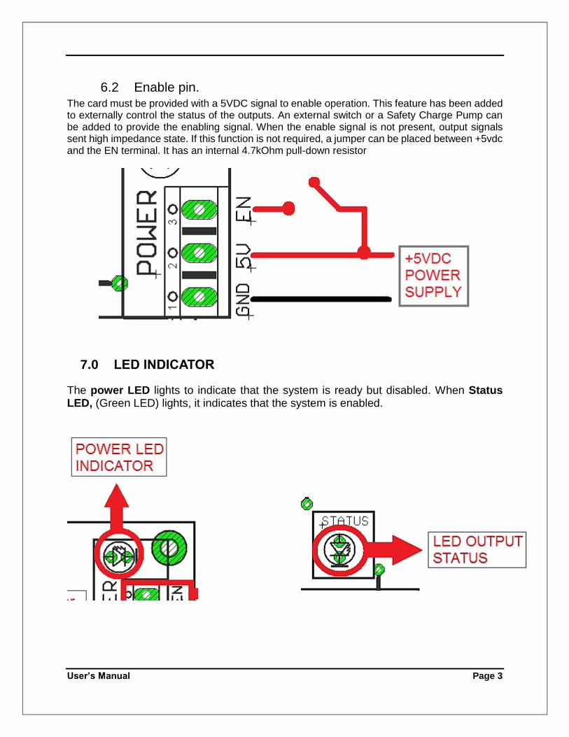
6.2 Enable pin. The card must be provided with a 5VDC signal to enable operation. This feature has been added to externally control the status of the outputs. An external switch or a Safety Charge Pump can be added to provide the enabling signal. When the enable signal is not present, output signals sent high impedance state. If this function is not required, a jumper can be placed between +5vdc and the EN terminal. It has an internal 4.7kOhm pull-down resistor
7.0 LED INDICATOR
The power LED lights to indicate that the system is ready but disabled. When Status LED, (Green LED) lights, it indicates that the system is enabled.
User’s Manual Page 4
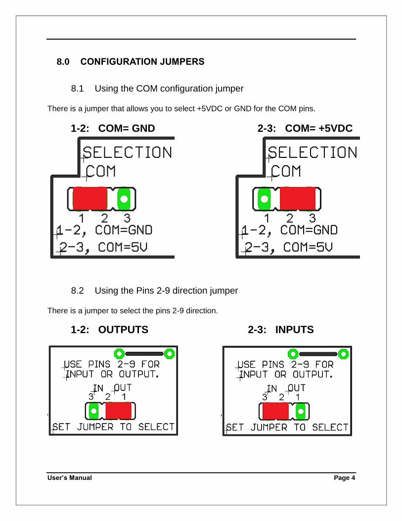
8.0 CONFIGURATION JUMPERS
8.1 Using the COM configuration jumper
There is a jumper that allows you to select +5VDC or GND for the COM pins.
1-2: COM= GND 2-3: COM= +5VDC
8.2 Using the Pins 2-9 direction jumper
There is a jumper to select the pins 2-9 direction.
1-2: OUTPUTS 2-3: INPUTS
User’s Manual Page 5
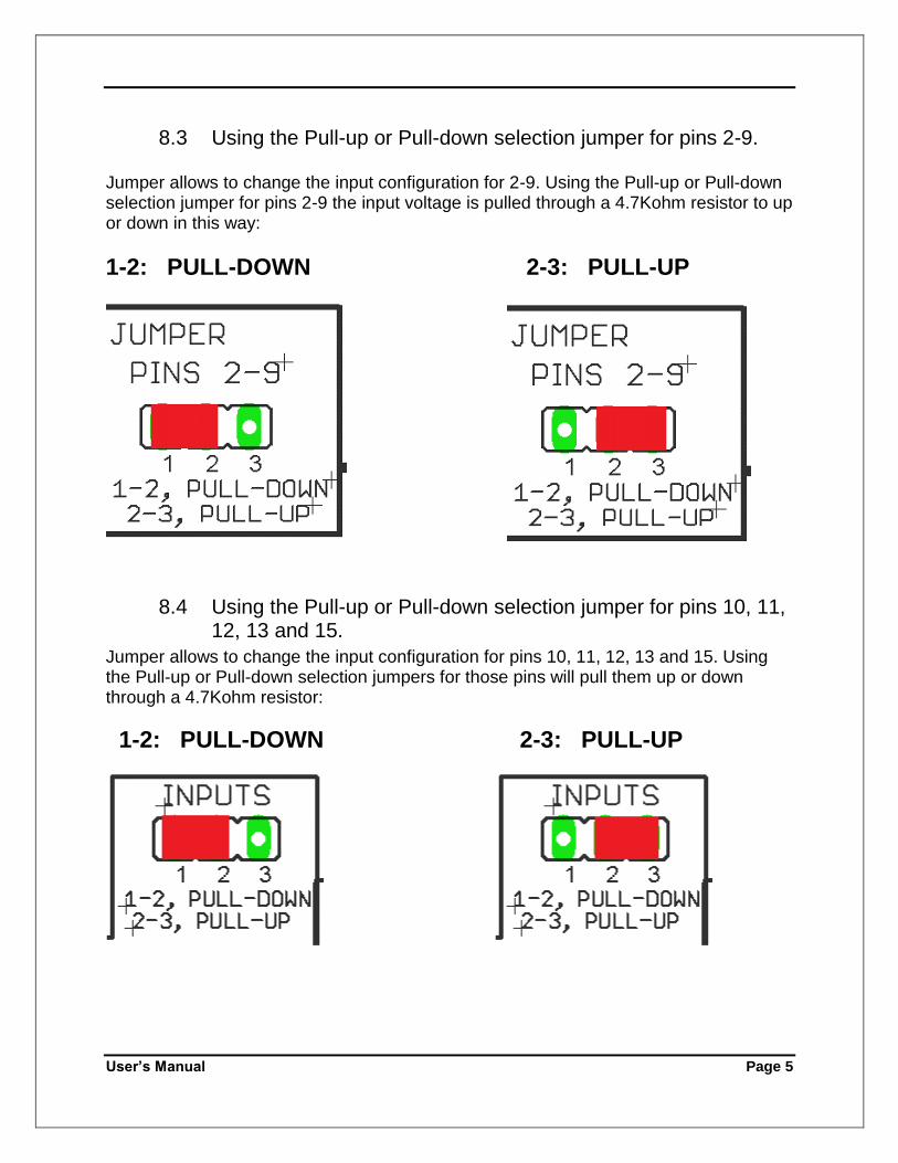
8.3 Using the Pull-up or Pull-down selection jumper for pins 2-9.
Jumper allows to change the input configuration for 2-9. Using the Pull-up or Pull-down selection jumper for pins 2-9 the input voltage is pulled through a 4.7Kohm resistor to up or down in this way:
1-2: PULL-DOWN 2-3: PULL-UP
8.4 Using the Pull-up or Pull-down selection jumper for pins 10, 11, 12, 13 and 15.
Jumper allows to change the input configuration for pins 10, 11, 12, 13 and 15. Using the Pull-up or Pull-down selection jumpers for those pins will pull them up or down through a 4.7Kohm resistor:
1-2: PULL-DOWN 2-3: PULL-UP
User’s Manual Page 6
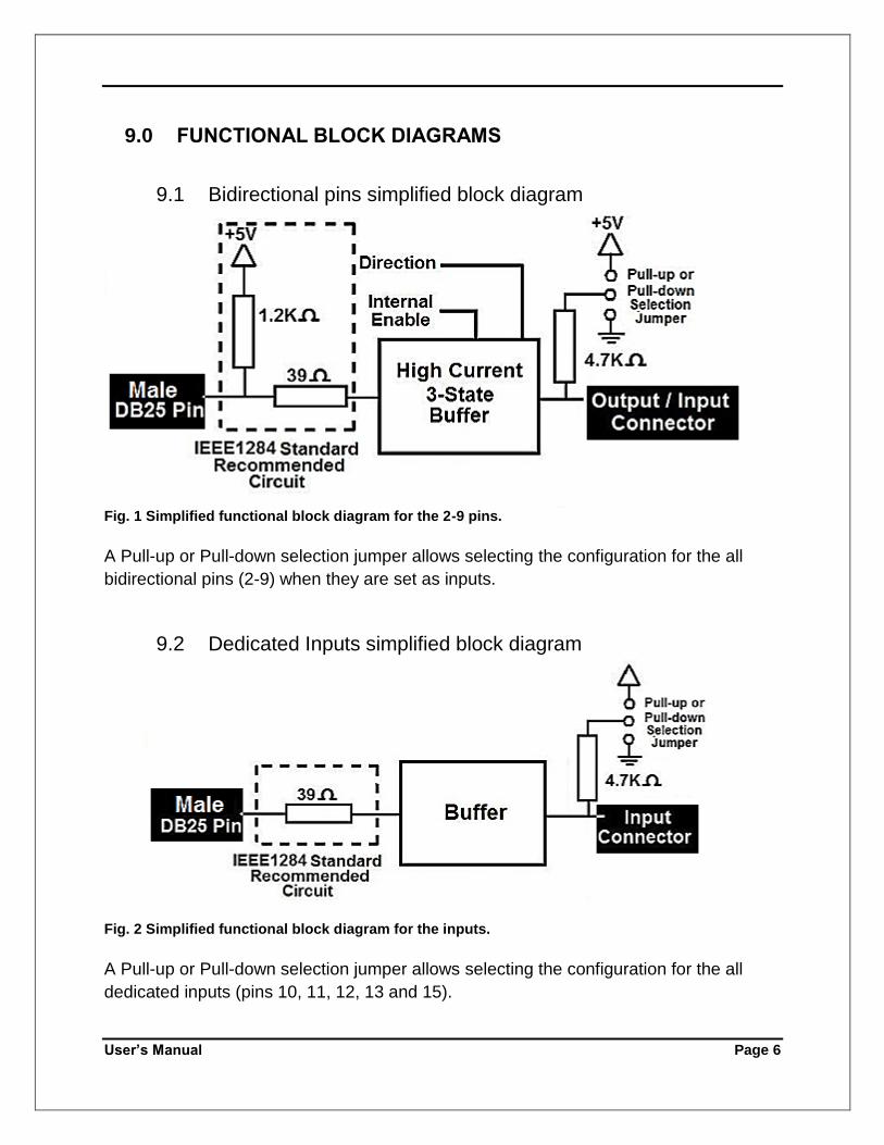
9.0 FUNCTIONAL BLOCK DIAGRAMS
9.1 Bidirectional pins simplified block diagram
Fig. 1 Simplified functional block diagram for the 2-9 pins.
A Pull-up or Pull-down selection jumper allows selecting the configuration for the all
bidirectional pins (2-9) when they are set as inputs.
9.2 Dedicated Inputs simplified block diagram
Fig. 2 Simplified functional block diagram for the inputs.
A Pull-up or Pull-down selection jumper allows selecting the configuration for the all
dedicated inputs (pins 10, 11, 12, 13 and 15).
User’s Manual Page 7
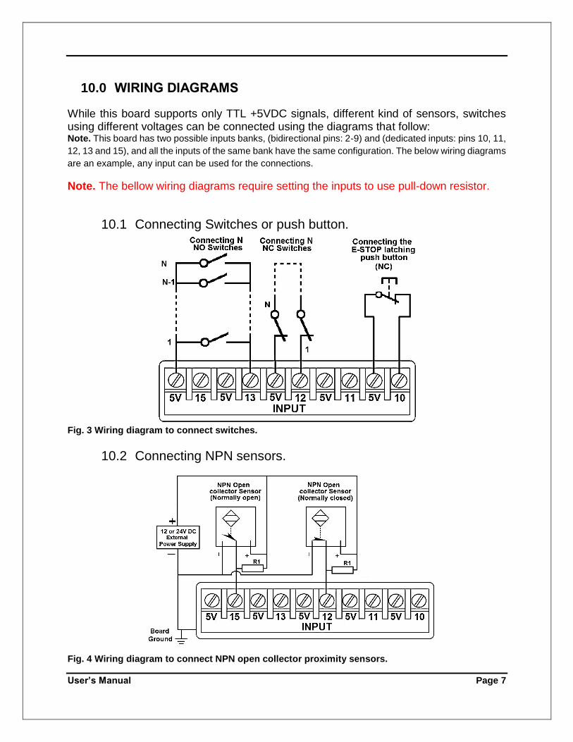
10.0 WIRING DIAGRAMS
While this board supports only TTL +5VDC signals, different kind of sensors, switches using different voltages can be connected using the diagrams that follow: Note. This board has two possible inputs banks, (bidirectional pins: 2-9) and (dedicated inputs: pins 10, 11,
12, 13 and 15), and all the inputs of the same bank have the same configuration. The below wiring diagrams
are an example, any input can be used for the connections.
Note. The bellow wiring diagrams require setting the inputs to use pull-down resistor.
10.1 Connecting Switches or push button.
Fig. 3 Wiring diagram to connect switches.
10.2 Connecting NPN sensors.
Fig. 4 Wiring diagram to connect NPN open collector proximity sensors.
User’s Manual Page 8
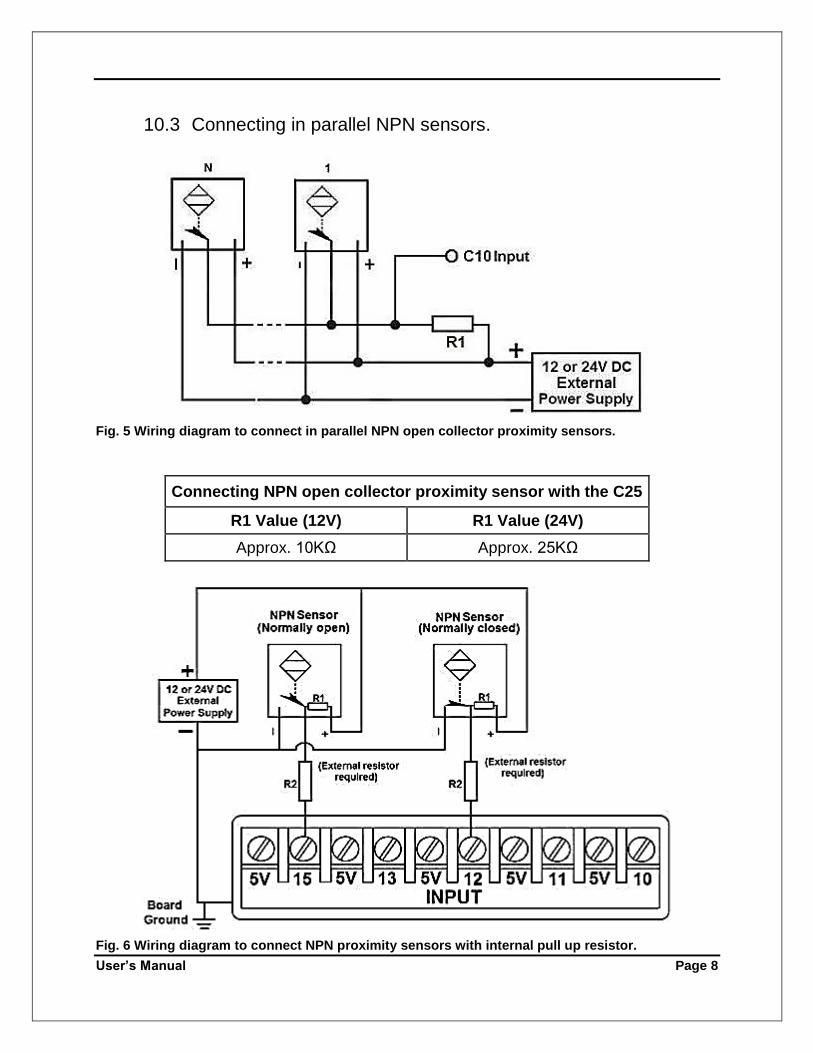
10.3 Connecting in parallel NPN sensors.
Fig. 5 Wiring diagram to connect in parallel NPN open collector proximity sensors.
Connecting NPN open collector proximity sensor with the C25
R1 Value (12V) R1 Value (24V)
Approx. 10KΩ Approx. 25KΩ
Fig. 6 Wiring diagram to connect NPN proximity sensors with internal pull up resistor.
User’s Manual Page 9
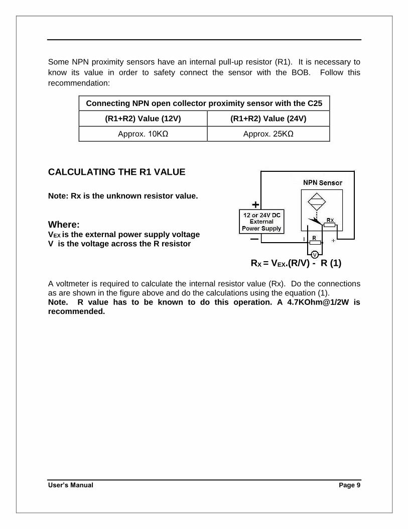
Some NPN proximity sensors have an internal pull-up resistor (R1). It is necessary to
know its value in order to safety connect the sensor with the BOB. Follow this
recommendation:
Connecting NPN open collector proximity sensor with the C25
(R1+R2) Value (12V) (R1+R2) Value (24V)
Approx. 10KΩ Approx. 25KΩ
CALCULATING THE R1 VALUE
Note: Rx is the unknown resistor value.
Where: VEX is the external power supply voltage
V is the voltage across the R resistor
RX = VEX.(R/V) - R (1) A voltmeter is required to calculate the internal resistor value (Rx). Do the connections as are shown in the figure above and do the calculations using the equation (1). Note. R value has to be known to do this operation. A 4.7KOhm@1/2W is recommended.
User’s Manual Page 10
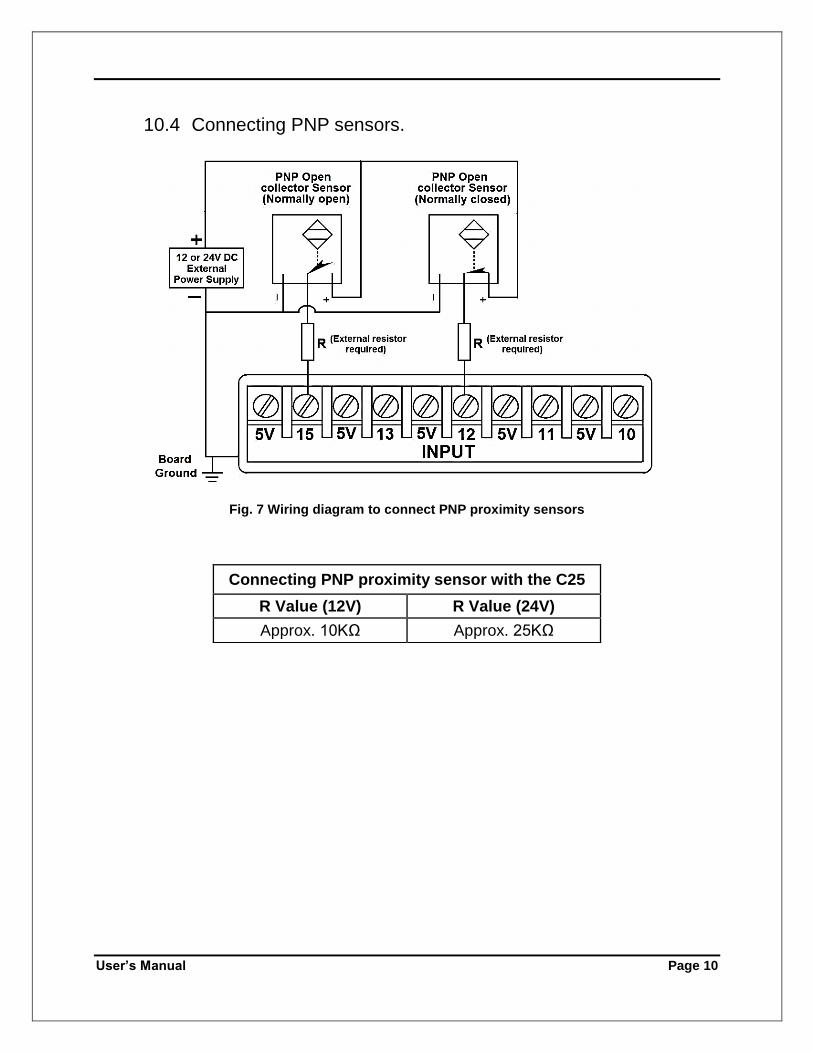
10.4 Connecting PNP sensors.
Fig. 7 Wiring diagram to connect PNP proximity sensors
Connecting PNP proximity sensor with the C25
R Value (12V) R Value (24V)
Approx. 10KΩ Approx. 25KΩ
User’s Manual Page 11
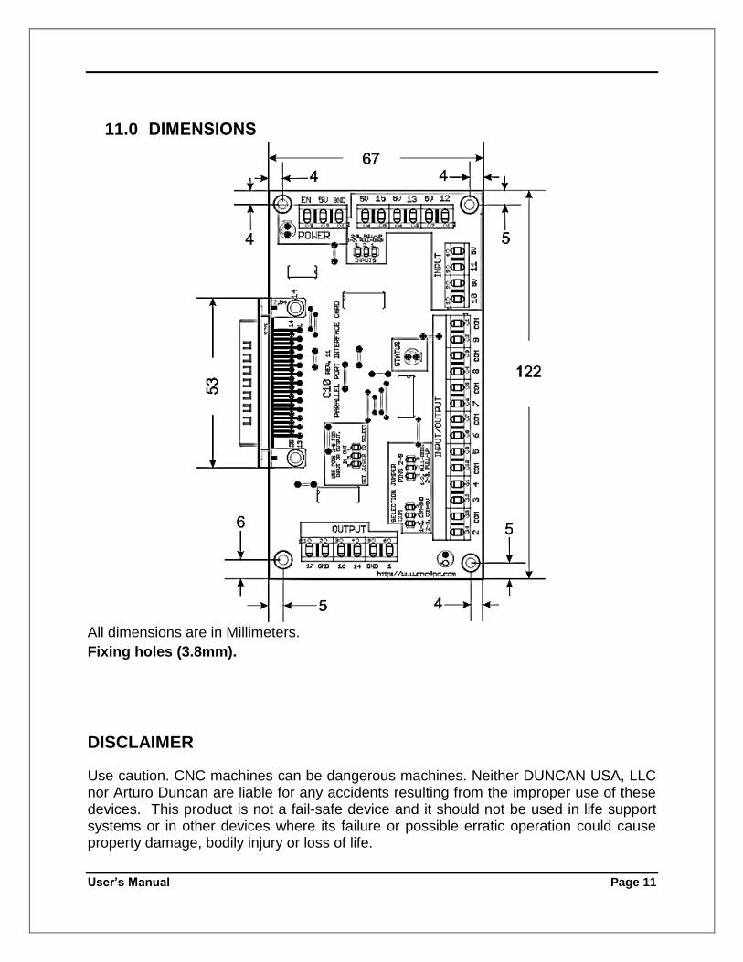
11.0 DIMENSIONS
All dimensions are in Millimeters.
Fixing holes (3.8mm).
DISCLAIMER
Use caution. CNC machines can be dangerous machines. Neither DUNCAN USA, LLC nor Arturo Duncan are liable for any accidents resulting from the improper use of these devices. This product is not a fail-safe device and it should not be used in life support systems or in other devices where its failure or possible erratic operation could cause property damage, bodily injury or loss of life.
Recommended