8/2/2019 BU Cam Data Sheet
http://slidepdf.com/reader/full/bu-cam-data-sheet 1/18
OmniVision Technologies, Inc. 930 Thompson Place Sunnyvale, CA 94086 U.S.A.
Tel: (408) 733-3030 Fax: (408) 733-3061
e-mail: [email protected]
Website: http://www.ovt.com
OV7910/OV7410/OV7411
Prel iminary
Version 1.4, December 7, 1999
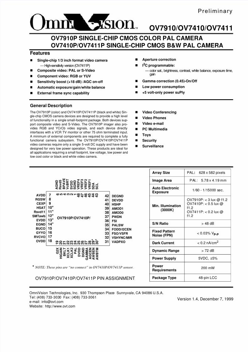
Array Size PAL: 628 x 582 pixels
Image Area PAL: 5.78 x 4.19 mm
Auto ElectronicExposure
1/60 - 1/15000 sec.
Min. Illumination(3000K)
OV7910P: < 3 lux @ f1.2OV7410P: < 0.5 lux @f1.2OV7411P: < 0.2 lux @f1.2
S/N Ratio > 48 dB
Fixed PatternNoise (FPN)
< 0.03% VP-P
Dark Current < 0.2 nA/cm2
Dynamic Range > 72 dB
Power Supply 5VDC, ±5%
PowerRequirements
200 mW
Package Type 48-pin LCCOV7910P/OV7410P/OV7411P PIN ASSIGNMENT
A G N D
R s v d 5
B P A V E
V c B
R T
S V D D
S G N D
V R E F 4
V R E F 3
V R E F 1
S D A
S C L
AVDD
RGSW
CEXP
HSAT
Rsvd11
SMTawb
EVDD
EGND
BUCO
GYYO
RVCVO
OVDD VADPXO
VSHYNC/MIR
FSO/VSFR
FODD/I2CEN
PALSW
FSI
PWDN
AMOD0
AMOD1
HSHP
DEVDD
DEGND
G 2 X
H I G A I N
B K L T
X C L K 1
X C L K 2
P A L
D G N D
G A M M A
A G C E N
D V D D
A W B E N
A W B T M
V R E F 2
6 5 4 3 2 1 4 8
4 7
4 6
4 5
4 4
4 37
8910*11*12*13*14*15161718 31
3233343536373839404142
1 9
2 0
2 1
2 2
2 3
2 4
2 5
2 6
2 7
2 8
2 9 *
3 0 *
OV7910P/OV7410P/
* NOTE: These pins are “no connect” in OV7410P/OV7411P sensor.
General Description
The OV7910P (color) and OV7410P/OV7411P (black and white) Sin-
gle-chip CMOS camera devices are designed to provide a high level
of functionality in a single small-footprint package. Both devices sup-
port composite video and S-Video. The OV7910P imager also pro-vides RGB and YCrCb video signals, and each device directly
interfaces with a VCR TV monitor or other 75 ohm terminated input.
A minimum of external components are required to complete a fully
functional camera subsystem. The OV7910P/OV7410P/OV7411P
video cameras require only a single 5-volt DC supply and have been
designed for very low power operation. These products are ideal for
all applications requiring a small footprint, low voltage, low power and
low cost color or black and white video camera.
n Video Conferencing
n Video Phones
n Video e-mailn PC Multimedia
n Toys
n Security
n Surveillance
OV7910P SINGLE-CHIP CMOS COLOR PAL CAMERAOV7410P/OV7411P SINGLE-CHIP CMOS B&W PAL CAMERA
Features
n
Single-chip 1/3 inch format video camera— High-sensitivity version (OV7411P)
n Composite video: PAL or S-Video
n Component video: RGB or YUV
n Sensitivity boost (+18 dB) /AGC on-off
n Automatic exposure/gain/white balance
n External frame sync capability
n Aperture correction
n I2C programmable:
— color sat., brightness, contrast, white balance, exposure timegain
n Gamma correction (0.45)-On/Off
n Low power consumption
n +5 volt-only power suPly

8/2/2019 BU Cam Data Sheet
http://slidepdf.com/reader/full/bu-cam-data-sheet 2/18

8/2/2019 BU Cam Data Sheet
http://slidepdf.com/reader/full/bu-cam-data-sheet 3/18
December 7, 1999 Version 1.4 3
OV7910P/OV7410P/OV7411P SINGLE IC CMOS COLOR & B/W PAL ANALOG CAMERAS
OMNIVISION TECHNOLOGIES, Inc.
Prel iminary
16 GYYO Output Video Output: Output format determined by pins 38 and 39 (AMOD1, AMOD0)
AMOD1 AMOD0 Output Component Format
0 0 S-Video YO channel Composite0 1 Green component RGB1 0 Y component YUV or B/W1 1 Green component RGB
Note: Modes (AMOD1, AMOD0) = 00, 01, 11 are not available for OV7410P Image Sensor
17 RVCVO Output Video Output: Output format determined by pins 38 and 39 (AMOD1, AMOD0)
AMOD1 AMOD0 Output Component Format
0 0 CVBS signal Composite0 1 Red component RGB1 0 Cr component YUV or B/W1 1 Red component RGB
Note: Modes (AMOD1, AMOD0) = 00, 01, 11 are not available for OV7410P Image Sensor
18 OVDD Vin Analog power for video output (+5VDC)
19 G2X Function(Default = 0)
Automatic Gain Control (AGC) gain selection. Affects range selected by HGAIN (p20). SeeHGAIN below.
“0” - select normal AGC gain (1X)“1” - select enhanced AGC gain (2X)
20 HGAIN Function(Default = 0)
Automatic Gain Control (AGC) gain range selection“0” - select normal AGC range (1X <-> 4X)“1” - select expanded AGC range (1X -> 8X)
HGAIN G2X AGC Range
0 0 1X <-> 4X0 1 2X <-> 8X1 0 1X <-> 8X1 1 2X <-> 16X
21 BKLT Function(Default = 0)
Backlight selection“0” - Disable backlight compensation“1” - Enable backlight compensation
22 XCLK1 CLK Crystal clock input. Frequency is 4 x Fsc to meet PAL subcarrier standards
23 XCLK2 CLK Crystal clock output (4 x Fsc for PAL = 17.73265 MHz)
24 PAL Function(Default = 1)
25 DVDD Vin Digital power
26 DGND Vin Digital ground
27 GAMMA Function
(Default = 1)
GAMMA selection
“0” - Disable GAMMA correction“1” - Enable GAMMA correction
28 AGCEN Function(Default = 1)
Automatic Gain Control (AGC) selection“0” - Disable AGC“1” - Enable AGC
29* AWBEN Function(Default = 1)(N/C on OV7410P/ OV7411P)
Automatic White Balance selection“0” - Disable AWB“1” - Enable AWB
Note: This function is not available on OV7410P/OV7411P Image Sensor. This pin is “no con-nect”.
Table 1. Pin Description
(Pins designated with “*” are “no connect” in OV7410P/OV7411P sensor.)
Pin No. Name Pin Type Function/Description

8/2/2019 BU Cam Data Sheet
http://slidepdf.com/reader/full/bu-cam-data-sheet 4/18
OV7910P/OV7410P/OV7411P
4 Version 1.4 December 7, 1999
SINGLE IC CMOS COLOR & B/W PAL ANALOG CAMERAS
OMNIVISION TECHNOLOGIES, Inc.
Prel iminary
30* AWBTM Function(Default = 0)(N/C on OV7410P/ OV7411P)
Automatic White Balance speed selection“0” - Select normal AWB“1” - Select “fast” AWB
Note: This function is not available on OV7410P/OV7411P Image Sensor. This pin is “no con-nect”.
31 VAXPXO Output Valid pixel detect output. CLK is asserted on this pin during active image period.
32 VHSYNC/MIR Output/Function(Default = 0)
Vertical/horizontal sync output. Adding a pullup resistor on this pin enables mirror image
33 FSO/VSFR Output/Function(Default = 0)
Vertical field/frame sync output, default to field sync. Adding a pullup resistor on this pin enablesframe sync.
34 FODD/I2CEN Output/Function(Default = 0)
Even/Odd field flag. Adding a pullup resistor on this pin enables I2C control.
35 PALSW Output PAL switch clock output
36 FSI Input Field sync input
37 PWDN Function Power Down mode selection“0” - Disable power down mode“1” - Enable power down mode
38 AMOD0 Function AMOD0 (w/AMOD1) selects output mode.
Note: This function is not available on OV7410P/OV7411P Image Sensor. This pin is “no con-nect”.
39 AMOD1 Function AMOD1 (w/AMOD0) selects output mode.
Note: This function is not available on OV7410P/OV7411P Image Sensor. This pin is “no con-nect”.
40 HSHP Function Sharpness level selection“0” - select normal sharpness“1” - select x2 sharpness
41 DEVDD Vin Analog power
42 DEGNZD Vin Analog ground
43 SCL Input/Output I2C control
44 SDA Input/Output I2C data/address
45 VREF1 Vref Internal reference. Must be decoupled with 0.1 µF capacitor to analog ground.
46 VREF2 Vref Internal reference. Must be decoupled with 0.1 µF capacitor to analog ground.
47 VREF3 Vref Internal reference. Must be decoupled with 0.1 µF capacitor to analog ground.
48 VREF4 Vref Internal reference. Must be decoupled with 0.1 µF capacitor to analog ground.
Table 1. Pin Description
(Pins designated with “*” are “no connect” in OV7410P/OV7411P sensor.)
Pin No. Name Pin Type Function/Description

8/2/2019 BU Cam Data Sheet
http://slidepdf.com/reader/full/bu-cam-data-sheet 5/18
December 7, 1999 Version 1.4 5
OV7910P/OV7410P/OV7411P SINGLE IC CMOS COLOR & B/W PAL ANALOG CAMERAS
OMNIVISION TECHNOLOGIES, Inc.
Prel iminary
1.1 Video Standards
Two TV standards are implemented and available asoutput in the OV7910P/OV7410P/OV7411P imaging
devices: PAL (B). Table 2 below shows how to config-
ure the standard of choice. Please note
that the accuracy and stability of the crystal clock frequency is important to avoid unwanted color shift in TV/
video systems.
1.2 Video Formats
The OV7910P/OV7410P/OV7411P image sensorssupport a variety of formats including Composite
(CVBS), S-Video (YO/CO), RGB components, YUV
components, and B/W. Composite and S-Video signals
are generated from the internal TV encoder and the
RGB/YUV/BW outputs are generated from the color
matrix prior to entering the encoder.
The image sensor utilizes the RG/BG Bayer pattern
sending raw pixel data through the color matrix, creating RGB or YUV component signals. At the same time
YUV signals are also processed to generate both com
posite and S-Video signals. (Note: Color format config
uration is valid only for the OV7910P image sensor)
1.2.1 Composite and S-Video
The Composite/S-Video format is the power-up defaul
Table 2. Standard Configuration
StandardPAL
(pin 24)Clock Comments
PAL 1 17.734475 MHz clock in = 4 x Fsc
configuration for the OV7910P/OV7410P/OV7411P
image sensors. Pins AMOD0/AMOD1 (pins 38 and 39)
select composite and S-Video formats. In this configu-
ration, RVCVO (pin 17) outputs CVBS, GYYO (pin 16)outputs
the YO component of the S-Video signal, and BUCO
(pin 15) outputs the CO component. Table 3 below
summarizes the formats available and the settings
required on the appropriate pins.
1.2.2 RGB
Setting AMOD0 = 1 (w/AMOD1 = x) selects the RGB
format. In this configuration, RVCVO outputs the
Red component, GYYO outputs the Green component
and BUCO provides the Blue component.
1.2.3 YUV
Setting AMOD0=0 and AMOD1=1 configures the
OV7910P/OV7410P/OV7411P sensors to operate in
YUV or B/W mode. In this configuration, GYYO outputs
the Y component, RVCVO provides the Cr component,
and BUCO outputs the Cb component. On the
OV7410P image sensor, only the GYYO (Y compo-
nent) output is valid.
1. Functional Description
(Note: All references to color functions apply only to OV7910P image sensor)

8/2/2019 BU Cam Data Sheet
http://slidepdf.com/reader/full/bu-cam-data-sheet 6/18
OV7910P/OV7410P/OV7411P
6 Version 1.4 December 7, 1999
SINGLE IC CMOS COLOR & B/W PAL ANALOG CAMERAS
OMNIVISION TECHNOLOGIES, Inc.
Prel iminary
Table 3. Video Format Selection
Format TypeRVCVO Output
(pin 17)
GYYO Output
(pin 16)
BUCO Output
(pin 15)Pin Settings
Composite + S-Video CVBS YO CO AMOD0 = 0, AMOD1 = 0
RGB Components Red Green BlueAMOD0 = 1, AMOD1 = x
YUV Components Cr Y CbAMOD0 = 0, AMOD1 = 1
Black and White — Y —
AMOD0 = 0, AMOD1 = 1
(Pins 15 & 17 are undefined on the OV7410P sen-sor)
1.3 Configuring the OV7910P/OV7410P/OV7411P
Image Sensors for Operation
The OV7910P/OV7410P/OV7411P sensors have been
designed for easy-of-use in many stand-alone applica-
tions. Most of the on-chip functions are configurable by
connecting appropriate pins high (logic “1”) or low
(logic “0”) through a 10k Ohm resistor. The image sen-
sor reads the input the pins at power up, which enables
user-defined default configurations.
The OV7910P/OV7410P/OV7411P imaging devices
also contain an I2C interface for programmatic access
to all
register functions (For further details on I2C, see Sec-
tion 2. “I2C Bus” on page 11). By default, the I2C port is
disabled. To enable the I2C for controlling the sensors,
a 10K Ohm pull-up resistor must be connected to
FODD/I2CEN. With FODD/I2CEN pulled high at
power-up, the OV7910P/OV7410P/OV7411P image
sensors will enable the I2C port for access.
1.4 White Balance
The function of white balance in the OV7910P image
sensor is to adjust and calibrate the image devices
sensitivity on the primary (RGB) colors to match the
color cast of the light source. The Auto White Balance
(AWB) can be enabled or disabled either through an
external pin (AWBEN, pin 29) or through the I2C port. If
AWB is enabled, the image sensors continuously per-
form white balancing. A fast or slow mode of white bal-ancing may be user-selected (AWBTM, pin 30). Fast
AWB updates color every 2 fields while slow
white balancing updates every 16 fields.
By using the I2C port, the color temperature may be
further fine tuned to the requirement of the application.
Note that the “blue” (Blue and Blue bias registers) and
“red” (Red and Red bias registers) bias control is avail-
able only through the I2C port. This function enables
the user to define a “cooler” or “warmer” background
for image capture.
1.5 Additional Picture Control
A number of functions/registers are available which
enable the user to configure OV7910P/OV7410P/
OV7411P image capturing parameters. These func-
tions include Automatic Gain Control (AGC), AGC
Gain, Automatic Exposure Control (AEC), GAMMA,
and Backlight control.
HGAIN (pin 20) may be used to set the range of AGC
Gain. A “0” on HGAIN sets AGC Gain range for 1X <->
4X, while a “1” sets the range for 1X <-> 8X. G2X (pin
19) can then be used to enhance the AGC gain range.
A “0” on G2X sets AGC gain at normal. A “1” enhances
the AGC gain by 2 (Refer to Table 1, “Pin Description,”
on page 2, pins 19 and 20 for further details). This
function may be configured through the I2C port, as

8/2/2019 BU Cam Data Sheet
http://slidepdf.com/reader/full/bu-cam-data-sheet 7/18
December 7, 1999 Version 1.4 7
OV7910P/OV7410P/OV7411P SINGLE IC CMOS COLOR & B/W PAL ANALOG CAMERAS
OMNIVISION TECHNOLOGIES, Inc.
Prel iminary
well. GAMMA (pin 27) can be used to set the GAMMA
correction. BKLT (pin 21) controls how the OV7910P/
OV7410P/OV7411P image sensors manage backlight
conditions. These functions may also be controlled
through the I2C interface.
At power up, AGC and AEC are enabled. AGC can be
disabled at power up by configuring the AGCEN pin
(pin 28) as required. AEC cannot be enabled/disabled
externally and must be reprogrammed through the I2C
port.
1.6 Other Image Sensor Control Functions
Additional programmable functions for the OV7910P/
OV7410P/OV7411P image sensors include sharpness
adjustment, brightness level fine tune, color saturation
adjustment, mirror image control, and power down. All
of these functions (except power down) can be config-
ured either by an external pin or through the I2C inter-face.

8/2/2019 BU Cam Data Sheet
http://slidepdf.com/reader/full/bu-cam-data-sheet 8/18
OV7910P/OV7410P/OV7411P
8 Version 1.4 December 7, 1999
SINGLE IC CMOS COLOR & B/W PAL ANALOG CAMERAS
OMNIVISION TECHNOLOGIES, Inc.
Prel iminary
Specifications
Table 4. Electrical parameters (0oC to 70 oC, all voltages referenced to GND)
Symbol Descriptions Max Typ Min Units
Supply
VDD Supply voltage (VDD, DVDD) 5.25 5.0 4.75 V
IDD Supply Current in VDDs 40 - - mA
I2C
fscl SCL clock frequency 400 - - kHz
tf SDA fall time 300 - 20 + 0.1Csda ns
tidle Bus idle time - - 1.3 us
thdsta START hold time - - 0.6 us
t stps STOP set up time - - 0.6 us
tds SDA set up time - - 100 us
tdh SDA hold time - - 0 us
Clock input / Crystal Oscillator
fosc Resonator frequency 10 - 20 MHz
Load capacitor - 10 - pF
Parallel resistance 1M W
Rise/fall time for external clock input - 5 - ns
Duty cycle for external clock input 60 40 %
Misc. timing
tSYNC External FSI cycle time - 2 - frame
tPU Chip power up time 100 - - us
tPD Power up delay time - 10 - us
tPZ Power up low-z delay - 1000 - ns
VTO analog video output parameters
VTO analog video output parameters
Symbol Descriptions Max
Type
(OV7910P)
Type
(OV7410P/
OV7411P)Min Units
VTO-P Video peak signal level - 2.3 2.4 - V
VTO-B Video black signal level - 0.7 1.2 - V
VSYNC Video sync pulse amplitude - 0.7 0.4 - V
Ro Video output load 75 75 Ohm

8/2/2019 BU Cam Data Sheet
http://slidepdf.com/reader/full/bu-cam-data-sheet 9/18
December 7, 1999 Version 1.4 9
OV7910P/OV7410P/OV7411P SINGLE IC CMOS COLOR & B/W PAL ANALOG CAMERAS
OMNIVISION TECHNOLOGIES, Inc.
Prel iminary
Figure 1. Spectrum Response

8/2/2019 BU Cam Data Sheet
http://slidepdf.com/reader/full/bu-cam-data-sheet 10/18
OV7910P/OV7410P/OV7411P
10 Version 1.4 December 7, 1999
SINGLE IC CMOS COLOR & B/W PAL ANALOG CAMERAS
OMNIVISION TECHNOLOGIES, Inc.
Prel iminary
Figure 2. Video Timing Diagram
( A ) H O R I Z O N T A L T I M I N G
( B ) V E R T I C A L T I M I N G
C H S Y N C
V T O
C H S Y N C
C H S Y N C
1
2
3
4
5 2 5
5 2 4
5 2 3
2 6
3
2 6 2
2 6 1
2 6 4
2 6 5 2 6 6
2 6 7
t H S Y N C
t H
t H B K
( C O M P O S I T E )
( H - S Y N C )
t V S Y N C
t V
V S Y N C

8/2/2019 BU Cam Data Sheet
http://slidepdf.com/reader/full/bu-cam-data-sheet 11/18
December 7, 1999 Version 1.4 11
OV7910P/OV7410P/OV7411P SINGLE IC CMOS COLOR & B/W PAL ANALOG CAMERAS
OMNIVISION TECHNOLOGIES, Inc.
Prel iminary
rate using a 7-bit address/data transfer protocol .
Figure 3. I2C Bus Protocol Format
S – START CONDITIONA – ACKNOWLEDGE BIT
P – STOP CONDITION
SLAVE ID - 1000000X
MSB LSB=0
X – RW BIT, 1: READ, 0:WRITE
1ST BYTE 2ND BYTE 3RD BYTE
S PAAARWSLAVE ID (7BIT) SUBADDRESS (8BIT) DATA (8BIT)
STARTSTOP
ACK
MSB LSB=1
1ST BYTE 2ND BYTE 3RD BYTE
S PAARWSLAVE ID (7BIT)
START
STOPACK
DATA (8BIT) DATA (8BIT)
MASTER TRANSMIT, SLAVE RECEIVE (WRITE CYCLE)
MASTER RECEIVE, SLAVE TRANSMIT (READ CYCLE)
– SLAVE TRANSMIT
– MASTER TRANSMIT
– MASTER INITIATE
NO ACK INLAST BYTE
ACK
1
MSB LSB=0
1ST BYTE 2ND BYTE
S PAARWSLAVE ID (7BIT) SUBADDRESS (8BIT)
START
STOP
ACK
MASTER TRANSMIT, SLAVE RECEIVE (DUMMY WRITE CYCLE)
2. I2C Bus
Many of the functions and configuration registers in the
OV7910P/OV7410P/OV7411P image sensors are
available through the I2C high-speed serial interface.
The I2C port is enabled by asserting the I2CEN line
(pin 34) through a 10K ohm resistor to VDD. When the
I2C
capability is enabled (I2CEN = 1),the OV7910P/
OV7410P/OV7411P imager operates as a slavedevice that supports up to 400 kbps serial transfer

8/2/2019 BU Cam Data Sheet
http://slidepdf.com/reader/full/bu-cam-data-sheet 12/18
OV7910P/OV7410P/OV7411P
12 Version 1.4 December 7, 1999
SINGLE IC CMOS COLOR & B/W PAL ANALOG CAMERAS
OMNIVISION TECHNOLOGIES, Inc.
Prel iminary
below).
Figure 4. Bit Transfer on the I2C Bus
SDA
SCL
DATA
STABLE
DATACHANGEALLOWED
2.1 I2C Bus Protocol Format
In I2C operation, the master must perform the following
operations:
n Generate the start/stop condition
n Provide the serial clock on SCL
n Place the 7-bit slave address, the RW bit,and the 8-bit subaddress on SDA
The receiver must pull down SDA during the acknowl-
edge bit time. During the write cycle, the OV7910P/
OV7410P/OV7411P device returns the acknowledg-
ment and, during read cycle, the master returns the
acknowledgment except when the read data is the last
byte. If the read data is the last byte, the master does
not perform an acknowledge, indicating to the slave
that the read cycle can be terminated. Note that the
restart feature is not supported here.
Within each byte, MSB is always transferred first.Read/write control bit is the LSB of the first byte. Stan-
dard I2C communications require only two pins: SCL
and SDA. SDA is configured as open drain for bidirec-
tional purpose. A HIGH to LOW transition on the SDA
while SCL is HIGH indicates a START condition. A
LOW to HIGH transition on the SDA while SCL is HIGH
indicates a STOP condition. Only a master can gener-
ate START/STOP conditions.
Except for these two special conditions, the protocol
that SDA remain stable during the HIGH period of the
clock, SCL. Each bit is allowed to change state only
when SCL is LOW (See Figure 4. Bit Transfer on theI2C Bus and Figure 5. Data Transfer on the I2C Bus
I

8/2/2019 BU Cam Data Sheet
http://slidepdf.com/reader/full/bu-cam-data-sheet 13/18
December 7, 1999 Version 1.4 13
OV7910P/OV7410P/OV7411P SINGLE IC CMOS COLOR & B/W PAL ANALOG CAMERAS
OMNIVISION TECHNOLOGIES, Inc.
Prel iminary
in one bus cycle. A multi-byte cycle overwrites its original subaddress; therefore, if a read cycle immediately follows
a multi-byte cycle, you must insert a single-byte write cycle that provides a new subaddress.
The OV7910P/OV7410P/OV7411P supports a single slave ID. The ID is preset to 80 write and 81 for read.
In the write cycle, the second byte in I2C bus is the subaddress for selecting the individual on-chip registers, and
the third byte is the data associated with this register. Writing to an undefined subaddress is ignored.
In the read cycle, the second byte is the data associated with the previous stored subaddress. Reading of unde-fined subaddresses returns unknown data.
2.2 Register Set
The table below provides a list and description of available I2C registers contained in the OV7910P/OV7410P/
OV7411P image sensor.
Table 5. I2C Registers
Subad-
dress
(hex)
RegisterDefault
(hex)
Read/
WriteDescriptions
00 Gain[6:0] 00 RW
GC[7] - unimplemented bit, returns ‘X’ when read.GC[6:0] – Storage for the current AGC Gain setting.
This register is updated automatically. If AGC is enabled, the internal control stores the optimalgain value in this register. IF AGC is not enabled, a “00” is stored in this register.
01 Blue[7:0] 80 RW
Storage for the current blue channel setting for white balance control.BLU[7] – “0” decrease gain, “1” increase gain.BLU[6:0] – blue channel gain balance value.
Note: This function is not available on the OV7410P/OV7411P Image Sensor.
02 Red[7:0] 80 RW
Storage for the current red channel setting for white balance control.RED[7] – “0” decrease gain, “1” increase gain.RED[6:0] – red channel balance value.
Note: This function is not available on the OV7410P/OV7411P Image Sensor.
03 Sat D0 RWSAT[7:0] – saturation adjustment. “FFh”- highest, “00h”-lowest
Note: This function is not available on the OV7410P/OV7411P Image Sensor.
04 Cnt 00 RW CTR[7:0] – contrast adjustment. “FFh”-highest, “00h”-lowest
05 Brt 80 RW BRT[7:0] – brightness adjustment. “FFh”-highest,“00h”-lowest
06 Rsvd06 B2 RW reserved
07 Blue Bias 20 RW
BBS[7:6] – rsvd (BBS[7:6] = 00)BBS[5:0] – blue channel bias value.
This value defines the fine tune adjustment for the blue tint in the white balance control. This reg-ister is the manual control portion of the AWB control
Note: This function is not available on the OV7410P/OV7411P Image Sensor.
Figure 5. Data Transfer on the I2C Bus
The OV7910P/OV7410P/OV7411P I2C supports multi
byte write and multi-byte read. The master must supply
the subaddress. in the write cycle, but not in the read
cycle. Therefore, the OV7910P/OV7410P/OV7411Ptakes the read subaddress from the previous write
cycle. In multi-byte write or multi-byte read cycles, the
subaddress is automatically increment after the first
data byte so that continuous locations can be accessed
SDA
SCL
S
A
SLAVE ID
RW
SUB AD

8/2/2019 BU Cam Data Sheet
http://slidepdf.com/reader/full/bu-cam-data-sheet 14/18
OV7910P/OV7410P/OV7411P
14 Version 1.4 December 7, 1999
SINGLE IC CMOS COLOR & B/W PAL ANALOG CAMERAS
OMNIVISION TECHNOLOGIES, Inc.
Prel iminary
08 Red Bias 20 RW
RBS[7:6] – rsvd (RBS[7:6] = 01)RBS[5:0] – red channel bias value.
This value defines the fine tune adjustment for the red tint in the white balance control. This reg-ister is the manual control portion of the AWB control
Note: This function is not available on the OV7410P/OV7411P Image Sensor.
09 Rsvd09 B7 RW reserved
0A Rsvd0A 45 RW reserved
0B Rsvd0B — W reserved
0C Rsvd0C — W reserved
0D Rsvd0D 4E RW reserved
0E Rsvd0E 32 RW reserved
0F Rsvd0F 7A RW reserved
10 version 03 R Version
11 Manufacture ID (H) 7F R MIDH[7:0] – manufacture ID high byte
12 Manufacture ID (L) A2 R MIDL[7:0] – manufacture ID low byte
13 AEC 82 RW AEC[7:0] – Manual exposure setting. “00” = lowest, 82 = Highest
14 Common A 9F RW
COMA[7] - CEXP, “0” selects central exposureCOMA[6:4] - rsvdCOMA[3] - GAMMA, “1” selects gamma = 0.45, “0” select gamma=1.0COMA[2] - AGCEN, “1” enables auto gain controlCOMA[1] - AWBEN “1” enables auto white balance*COMA[0] - AEC enable. If AEC is enabled, the AEC register (Reg. 13) is updated automatically.
If AEC is disabled, AEC register remains unchanged.
*Note: COMA[1], AWBEN is not available on the OV7410P/OV7411P Image Sensor.
15 Common B 00 RW
COMB[7] - SRST, “1” initiates soft reset. Initiate soft reset. All registers are set to default valuesand chip is reset to known state and resumes normal operation. This bit is automaticallycleared after reset.
COMB[6]] - MIRR, “1” selects mirror imageCOMB[5]] - VSFR, “1” enables frame sync output to VSYNC (pin 32), “0” enables field sync
ouput to VSYNCCOMB[4]] - BKLT, “1” selects backlight exposure modeCOMB[3]] - FREX, “1” disables the update of exposure and gain value
COMB[2] - HGAIN. Automatic Gain Control (AGC) gain range selection. See COME[6] (G2X),below.
“0” - select normal AGC range (1X <-> 4X)“1” - select expanded AGC range (1X -> 8X)
HGAIN G2X AGC Range
0 0 1X <-> 4X0 1 2X <-> 8X1 0 1X <-> 8X1 1 2X <-> 16X
COMB[1:0] - AMOD, select video output modes00 - S-video and CVBS*01 - RGB* 10 - YUV11 - RGB*
*Note: COMB[1:0] = 00, 01, 11 are not available on the OV7410P/OV7411P Image Sensor.
16 Common C 20 RWCOMC[7] - Smart AWB. “0” disables SMTawb, “1” enables SMTawbCOMC[6] - rsvdCOMC[5] - Automatic Level Control. “0” disables ALC, “1” enables ALCauto level controlCOMC[4:0] - rsvd
17 Common D 34 RW
COMD[7:4] - rsvdCOMD[3] - BPSHP. “0” enables sharpness control, “1” disables sharpness controlCOMD[2] - rsvdCOMD[1] -AWBTM, “1” selects fast AWB update*COMD[0] - rsvd
*Note: COMD[1], AWBTM is not available on the OV7410P/OV7411P Image Sensor.
18 Rsvd18 A2 RW reserved
19 Rsvd19 66 RW reserved
Subad-
dress
(hex)
RegisterDefault
(hex)
Read/
WriteDescriptions

8/2/2019 BU Cam Data Sheet
http://slidepdf.com/reader/full/bu-cam-data-sheet 15/18
December 7, 1999 Version 1.4 15
OV7910P/OV7410P/OV7411P SINGLE IC CMOS COLOR & B/W PAL ANALOG CAMERAS
OMNIVISION TECHNOLOGIES, Inc.
Prel iminary
1A Rsvd1A 73 RW reserved
1B Rsvd1B D0 RW reserved
1C Rsvd1C 15 RW reserved
1D Common E 20 RW
COME[7] - rsvdCOME[6] - G2XA. Automatic Gain Control (AGC) gain selection. Affects range selected by
HGAIN. See COMB[2] (HGAIN), above.“0” - select normal AGC gain (1X)“1” - select enhanced AGC gain (2X)
COME[5:0] - rsvd
1E Rsvd1F 30 RW reserved
1F Rsvd20 28 RW reserved
20 - 2F Rsvd2X N/A RW reserved
30 Rsvd30 80 RW reserved
31 Rsvd31 80 RW reserved
32 Rsvd32 80 RW reserved
33 Rsvd33 40 RW reserved
34 Rsvd34 80 RW reserved
35 Rsvd35 20 RW reserved36 Rsvd36 20 RW reserved
37 Rsvd37 80 RW reserved
38 Rsvd38 80 RW reserved
39 Rsvd39 80 RW reserved
3A Rsvd3A 80 RW reserved
3B Rsvd3B 80 RW reserved
Subad-
dress
(hex)
RegisterDefault
(hex)
Read/
WriteDescriptions

8/2/2019 BU Cam Data Sheet
http://slidepdf.com/reader/full/bu-cam-data-sheet 16/18
OV7910P/OV7410P/OV7411P
16 Version 1.4 December 7, 1999
SINGLE IC CMOS COLOR & B/W PAL ANALOG CAMERAS
OMNIVISION TECHNOLOGIES, Inc.
Prel iminary
31
30
19
18 7
6
43
42
48
+0.0100.060 -0.005
TYP.0.040 ±0.007
TYP.
0.440 ±0.005
0.040 ±0.003
0.085 ±0.010
0.020 ±0.003TYP.
R 0.007548 PLCS
R 0.00754 CORNERS
0.003
0.002
0.020 ±0.002
0.015 ±0.0020.030
0.0030.065 ±0.007
±0.003
Bottom View
Top View
Side View
42
43
6 19
30
31
48
18
1
7
42
43
31
30
19
18
6
7
0.006 MAX.0.002 TYP.
0.350 SQ. ±0.005
0.430 SQ. ±0.005
0.560 SQ. -0.005+0.012
0 . 0 3
6 M I N .

8/2/2019 BU Cam Data Sheet
http://slidepdf.com/reader/full/bu-cam-data-sheet 17/18
December 7, 1999 Version 1.4 17
OV7910P/OV7410P/OV7411P SINGLE IC CMOS COLOR & B/W PAL ANALOG CAMERAS
OMNIVISION TECHNOLOGIES, Inc.
Prel iminary
Figure 6. OV7910P/OV7410P/OV7411P Package Outline
OmniVision Technologies, Inc. reserves the right to make changes without further notice to any product herein to improve reliability, function, or
design. OmniVision Technologies, Inc. does not assume any liability arising out of the application or use of any product or circuit described
herein; neither does it convey any license under its patent rights nor the rights of others. No part of this publication may be copied or repro-
duced, in any form without the prior written consent of OmniVision Technologies, Inc.
Table 6. Ordering InformationPart Number Description Package
OV7910P Color Image Sensor, PAL Analog, I2C Bus Control 48 pin LCC
OV7410P B/W Image Sensor, PAL Analog, I2C Bus Control 48 pin LCC
OV7411P High sensitivity B/W Image Sensor w/micro lenses, PAL Analog, I2C Bus Control 48 pin LCC
1
Sensor
Array
DIE
Package Center(0, 0)
Array Center
(14.5 mil, 0.87mil)(368.3 µ, 22.1 µ)

8/2/2019 BU Cam Data Sheet
http://slidepdf.com/reader/full/bu-cam-data-sheet 18/18
OV7910P/OV7410P/OV7411P
18 Version 1.4 December 7, 1999
SINGLE IC CMOS COLOR & B/W PAL ANALOG CAMERAS
OMNIVISION TECHNOLOGIES, Inc.
Prel iminary
Revision History
Product
Product
Version Description Date
OV7910P/OV7410P AA Product Release 10/1/98
OV7910P/OV7410P AI Process/performance change enhancements 1/1/99
OV7910P/OV7410P AJ Process/performance change enhancements, I2Cregister changes: Regs. 03, 06, 08, x10
2/11/99
OV7910P/OV7410P AK Performance/manufacturability improvements 2/22/99
OV7910P/OV7410P AK Miscellaneous corrections 6/6/99
OV7910P/OV7410P/ OV7411P
AK Add OV7411P release 6/17/99
Recommended