
Data Sheet
Broadcom AR18-AR35-Series-DS100October 3, 2017
DescriptionThe Broadcom® AR18 and AR35 Series are the miniature Absolute Encoder ASIC designed to cater for the growing demand on the space constraint application.
The AR18 encoder is designed for an overall diameter of 18 mm and offers user-programmable resolution ranging from 17, 19, and 21 bit single-turn absolute output. The AR35 encoder is designed for an overall diameter of 35 mm and offers 17 and 21 bits single-turn absolute output.
Both the AR18 and AR35 series provide the incremental ABI and UVW in differential mode. Both come with a recommended high temperature range of –40°C to 115°C suitable for most industrial applications. Dual-mode operating voltage of 3.3V and 5V enable handheld and portable device applications.
Employing Broadcom patented Reflective Optical Encoding Theory, the AR18 and AR35 series offer a high accuracy with correction, which is unattainable by the magnetic encoder.
Features Miniature absolute encoder ASIC surface mount DFN
package: 10.9 mm (L) x 9.1 mm (W) x 1.5 mm (H) User-programmable resolution ranging from:
– 17, 19, and 21 bit single turn (OD18).– 17 and 21 bit single turn (OD35).
User-programmable incremental output (ABI) resolution ranging from 128 to 8192 CPR
User-programmable commutation signal (UVW) ranging from 2, 3, 4, 5, 12, 30, 32 pole pair
Differential output for ABI and UVW High temperature range of –40°C to 115°C suitable for
most of the industrial operation. Dual-mode operating voltage of 3.3V and 5V, enabling
handheld and portable device applications. Selectable SSI mode communication protocol. Selectable RS485 mode communication protocol. RoHs compliance.
Applications Robotic automation and engineering Factory automation and drone Medical and dentistry, devices and equipment High-accuracy portable and handheld devices Miniature motor, servo motor, linear actuator
AR18 and AR35 Series Miniature Programmable Single-Turn Absolute Encoder with Resolution Ranging from 17 bits to 21 Bits

Broadcom AR18-AR35-Series-DS1002
AR18 and AR35 Series Data Sheet Miniature Programmable Single-Turn Absolute Encoder with Resolution Ranging from 17
bits to 21 Bits
Functional Block Diagram
With SSI 3-Wire Communication Protocol SelectionFigure 1: SSI 3-Wire Block Diagram
With ESL Communication Protocol SelectionFigure 2: ESL Block Diagram
Vcc
TST0
Analog I/Os
3.3V/5.0V
PDA
GND
LED Regulation
Analog Front End
ADC
(SinP/SinN/ CosP/CosN)
Digital Processing
MTP InterfaceSPI
EXT EEPROM
EEPROM_*(Ext EEPROM I2C interface)
A / Probe 1B / Probe 2I / Probe 3
U / Probe 4VW
NSL
SSI 3 Wire
SCLKDOUT
SPI CLKSPI DINSPI DOUT
TST1
TST2
TST3
Vcc
TST0
Analog I/Os
3.3V/5.0V
PDA
GND
LED Regulation
Analog Front End
ADC
(SinP/SinN/ CosP/CosN)
Digital Processing
MTP InterfaceSPI
EXT EEPROM
EEPROM_*(Ext EEPROM I2C interface)
A / Probe 1B / Probe 2I / Probe 3
U / Probe 4VW
ESL
RS485+ RS485-
TST1
TST2
TST3
EXT OSC

Broadcom AR18-AR35-Series-DS1003
AR18 and AR35 Series Data Sheet Miniature Programmable Single-Turn Absolute Encoder with Resolution Ranging from 17
bits to 21 Bits
Mechanical Specifications
DFN Package DimensionsFigure 3: Overall Package Dimensions and Pinout
Note: All dimensions given in mm. Tolerances of form and position according to JEDEC MO-220.
Package MarkingsFigure 4: Product Marking Information
Part Type
A18S/EA35S/E
Date Code
YYWW (Year, Work Week)

Broadcom AR18-AR35-Series-DS1004
AR18 and AR35 Series Data Sheet Miniature Programmable Single-Turn Absolute Encoder with Resolution Ranging from 17
bits to 21 Bits
Encoder MountingFigure 5: Encoder Mounting Guide
Notes of assembly: The assembly of the encoder needs clean room condition, Class 100k or better. The encoder needs to be enclosed with IP50 enclosure.
AR35 AR18

Broadcom AR18-AR35-Series-DS1005
AR18 and AR35 Series Data Sheet Miniature Programmable Single-Turn Absolute Encoder with Resolution Ranging from 17
bits to 21 Bits
Recommended PCB Land PatternFigure 6: PCB Land Pattern
Electrical Specifications
Recommended Operating Conditions
Parameter Symbol
Value
Unit NotesMin Typical MaxDC Supply Voltage Vdd +4.5 +5.0 +5.5 V
DC Supply Voltage Vdd +3.0 +3.3 +3.6 V
Ripple of Supply Voltage — — 100 mVpp 100 kHzAmbient Temperature Tamb — +25 — °C
Operational Temperature TA –40 +25 +115 °C
Storage Temperature TS –40 +25 +115 °C
Humidity RH — — 85 % Temp = 40°CINC Operating Frequency — — 128 kHz Velocity (rpm) x CPR/60Radial Misalignment –200 0 +200 μmTangential Misalignment –200 0 +200 μmEncoder Shaft Speed SRPM — — 30000 rpm 256CPR (AR18)Encoder Shaft Speed SRPM — — 15000 rpm 512CPR (AR35)
SMT Reflow Profile: JEDEC Pb-Free (J-STD-020D)
PIN-18PIN-17
Broadcom AR18-AR35-Series-DS1006
AR18 and AR35 Series Data Sheet Miniature Programmable Single-Turn Absolute Encoder with Resolution Ranging from 17
bits to 21 Bits
Absolute Maximum Ratings
DC CharacteristicsDC characteristics over recommended operating range, typical at 25°C.
Encoder CharacteristicsIncremental encoder characteristics over recommended operating range, at 25°C.
Encoder Pin FunctionsFigure 7: Pinouts from Top View
Parameter Symbol ValueStorage Temperature TS –40°C to 115°C
Operating Temperature TA –40°C to 115°C
Supply Voltage Vdd 7V
Moisture Sensitive Level 3 (Maximum floor life = 168h)
Parameter Symbol Conditions
Value
Unit Notes Min Typ. MaxVdd Supply Current Idd Vdd = 3.3V/5V — 70 — mA
Absolute Single-Turn Resolution (AR18)
— 17, 19, and 21 — Bit
Absolute Single-Turn Resolution (AR35)
— 17 and 21 — Bit
Incremental Resolution — 2n — CPR n = 7, 8, 9,10, 11, 12, 13
Parameter Symbol Min Typ Maxa
a. Maximum values represent the encoder performance across the range of recommended mounting tolerance.
UnitCycle Error ΔC — — 45 °eState Error ΔS — — 45 °eIndex Pulse Width Po — 90,180, 360 — °e

Broadcom AR18-AR35-Series-DS1007
AR18 and AR35 Series Data Sheet Miniature Programmable Single-Turn Absolute Encoder with Resolution Ranging from 17
bits to 21 Bits
SSI 3-Wire Option Pinout ConfigurationNOTE: Pin 35 must be grounded to VSSA and pin 17 connect to common GND.
Table 1: SSI 3-Wire Pinout
Pin Name Function Pad Type Analog/DigitalInput/ Output
1 CN/TST3 Analog Voltage Output NCOS 5V/3.3V pads Analog I/O2 CP/TST2 Analog Voltage Output PCOS 5V/3.3V pads Analog I/O3 SN/TST1 Analog Voltage Output NSIN 5V/3.3V pads Analog I/O4 SP/TST0 Analog Voltage Output PSIN 5V/3.3V pads Analog I/O5 SPI DOUT SPI Data Output 3.3V/5V (VDDPAD) Digital Output6 SPI DIN SPI Data Input 3.3V/5V (VDDPAD) Digital Input7 SPI CLK SPI Clock 3.3V/5V (VDDPAD) Digital Input8 VDD Digital Supply Voltage 3.3V/5V (VDDPAD) Digital Power9 VSS Digital GND Digital ground Digital ground Ground
10 + SSI DOUT SSI Data Output (+) 3.3V/5V (VDDPAD) Digital I/O11 – SSI DOUT SSI Data Output (–) 3.3V/5V (VDDPAD) Digital I/O12 + SSI NSL SSI Input (+) 3.3V/5V (VDDPAD) Digital I/O13 – SSI NSL SSI Input (–) 3.3V/5V (VDDPAD) Digital Input14 + SSI SCL SSI Clock (+) 3.3V/5V (VDDPAD) Digital Input15 – SSI SCL SSI Clock (–) 3.3V/5V (VDDPAD) Digital Input1617 ESL SEL Protocol Selection Selection (GND) Ground Ground18 EEPROM SCL EXT EEPROM Clock 3.3V/5V (VDDPAD) Digital I/O19 EEPROM SDA EXT EEPROM Data 3.3V/5V (VDDPAD) Digital I/O20 EEPROM WP EXT EEPROM Write Protect 3.3V/5V (VDDPAD) Digital Output21 –A Incremental –A Output 3.3V/5V (VDDPAD) Digital Output22 +A/PROBE1 Incremental +A Output 3.3V/5V (VDDPAD) Digital Output23 –B Incremental –B Output 3.3V/5V (VDDPAD) Digital Output24 +B/PROBE2 Incremental +B Output 3.3V/5V (VDDPAD) Digital Output25 –I Incremental –Index Output 3.3V/5V (VDDPAD) Digital Output26 +I/PROBE3 Incremental +Index Output 3.3V/5V (VDDPAD) Digital Output27 VSSA Analog GND Analog ground Analog ground Ground28 VDDA Analog Supply Voltage 3.3V/5V (VDDPAD) Analog Power29 –U Incremental –U Output 3.3V/5V (VDDPAD) Digital Output30 +U/PROBE4 Incremental +U Output 3.3V/5V (VDDPAD) Digital Output31 –V Incremental –V Output 3.3V/5V (VDDPAD) Digital Output32 +V Incremental +V Output 3.3V/5V (VDDPAD) Digital Output33 –W Incremental –W Output 3.3V/5V (VDDPAD) Digital Output34 +W Incremental +W Output 3.3V/5V (VDDPAD) Digital Output35 Common GND (VSSA) Ground to VSSA Analog ground Analog ground Ground

Broadcom AR18-AR35-Series-DS1008
AR18 and AR35 Series Data Sheet Miniature Programmable Single-Turn Absolute Encoder with Resolution Ranging from 17
bits to 21 Bits
ESL Option Pinout ConfigurationNOTE: Pin 35 must be grounded to VSSA and pin 17 connect to VDD (5V/3.3V).
Table 2: ESL Pinout
Pin Name Function Pad Type Analog/DigitalInput/
Output1 CN/TST3 Analog Voltage Output NCOS 5V/3.3V pads Analog I/O2 CP/TST2 Analog Voltage Output PCOS 5V/3.3V pads Analog I/O3 SN/TST1 Analog Voltage Output NSIN 5V/3.3V pads Analog I/O4 SP/TST0 Analog Voltage Output PSIN 5V/3.3V pads Analog I/O5678 VDD Digital Supply Voltage 3.3V/5V (VDDPAD) Digital Power9 VSS Digital GND Digital ground Digital ground Ground
10 + RS485 RS485 Data Output (+) 3.3V/5V (VDDPAD) Digital I/O11 – RS485 RS485 Data Output (–) 3.3V/5V (VDDPAD) Digital I/O1213141516 OSC_EXT External Oscillator 3.3V pads Digital Input17 ESL SEL Protocol Selection Selection (VDD) Digital Power18 EEPROM SCL EXT EEPROM Clock 3.3V/5V (VDDPAD) Digital I/O19 EEPROM SDA EXT EEPROM Data 3.3V/5V (VDDPAD) Digital I/O20 EEPROM WP EXT EEPROM Write Protect 3.3V/5V (VDDPAD) Digital Output21 –A Incremental –A Output 3.3V/5V (VDDPAD) Digital Output22 +A/PROBE1 Incremental +A Output 3.3V/5V (VDDPAD) Digital Output23 –B Incremental –B Output 3.3V/5V (VDDPAD) Digital Output24 +B/PROBE2 Incremental +B Output 3.3V/5V (VDDPAD) Digital Output25 –I Incremental –Index Output 3.3V/5V (VDDPAD) Digital Output26 +I/PROBE3 Incremental +Index Output 3.3V/5V (VDDPAD) Digital Output27 VSSA Analog GND Analog ground Analog ground Ground28 VDDA Analog Supply Voltage 3.3V/5V (VDDPAD) Analog Power29 –U Incremental –U Output 3.3V/5V (VDDPAD) Digital Output30 +U/PROBE4 Incremental +U Output 3.3V/5V (VDDPAD) Digital Output31 –V Incremental –V Output 3.3V/5V (VDDPAD) Digital Output32 +V Incremental +V Output 3.3V/5V (VDDPAD) Digital Output33 –W Incremental –W Output 3.3V/5V (VDDPAD) Digital Output34 +W Incremental +W Output 3.3V/5V (VDDPAD) Digital Output35 Common GND (VSSA) Ground to VSSA Analog ground Analog ground Ground

Broadcom AR18-AR35-Series-DS1009
AR18 and AR35 Series Data Sheet Miniature Programmable Single-Turn Absolute Encoder with Resolution Ranging from 17
bits to 21 Bits
Communication Protocol
SSI 3-WireFigure 8: SSI 3-Wire Timing Diagram
Notes: NSL toggles from high to low to start request position data. SCL maximum frequency is 10 MHz.tREQ = 10 μs is the time of data request processing.
n cycle (depending on absolute resolution settings)
Figure 9: AR18 SSI 3-Wire Format Output Figure 10: AR35 SSI 3-Wire Format Output
Broadcom AR18-AR35-Series-DS10010
AR18 and AR35 Series Data Sheet Miniature Programmable Single-Turn Absolute Encoder with Resolution Ranging from 17
bits to 21 Bits
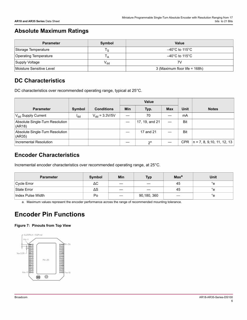
ESLFigure 11: General Transmission Frames Format on Half Duplex Line
Start of transmission frames set: Upon detected the first logic of Low state 0 on the transmission line after idling state, and if the following 3 bit conforms to command identifier, the encoder will acknowledge as a valid Request Command Frame (RCF), indicating the start of transmission frame set; else, it will continue to search for next available logic of low state 0.
End of transmission frames set: After the Request Command Frame is detected, if there is no Start Bit after the End Bit of the last frame read and no subsequent frame detected, end of transmission frame set is concluded.
Idle state: Idle state means a space between each transmission frames set and subsequent transmission frames. At idling state, logic of output in transmission line is kept to high state 1.
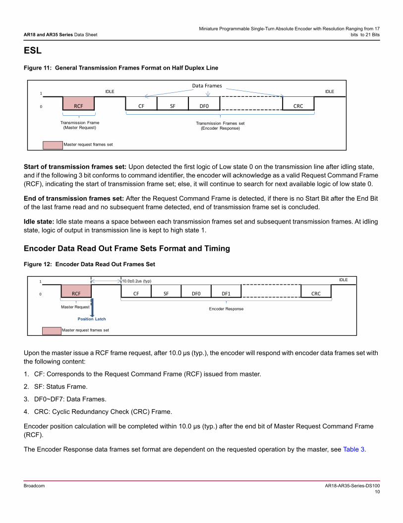
Encoder Data Read Out Frame Sets Format and Timing
Figure 12: Encoder Data Read Out Frames Set
Upon the master issue a RCF frame request, after 10.0 μs (typ.), the encoder will respond with encoder data frames set with the following content:
1. CF: Corresponds to the Request Command Frame (RCF) issued from master.
2. SF: Status Frame.
3. DF0~DF7: Data Frames.
4. CRC: Cyclic Redundancy Check (CRC) Frame.
Encoder position calculation will be completed within 10.0 μs (typ.) after the end bit of Master Request Command Frame (RCF).
The Encoder Response data frames set format are dependent on the requested operation by the master, see Table 3.
1 IDLE IDLE
0 RCF CF SF DF0 CRC
Master request frames set
Transmission Frame (Master Request)
Transmission Frames set (Encoder Response)
Data Frames
1 10.0±0.2us (typ) IDLE
0 RCF CF SF DF0 DF1 CRC
Master request frames set
Position Latch
Master Request Encoder Response
Broadcom AR18-AR35-Series-DS10011
AR18 and AR35 Series Data Sheet Miniature Programmable Single-Turn Absolute Encoder with Resolution Ranging from 17
bits to 21 Bits
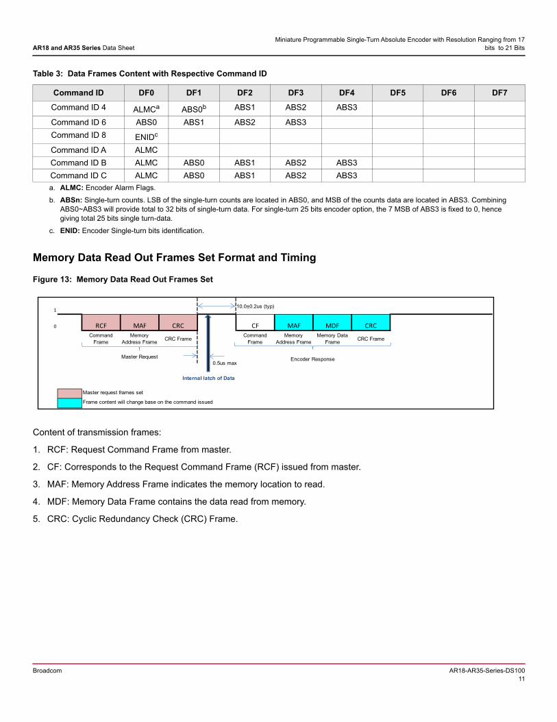
Memory Data Read Out Frames Set Format and Timing
Figure 13: Memory Data Read Out Frames Set
Content of transmission frames:
1. RCF: Request Command Frame from master.
2. CF: Corresponds to the Request Command Frame (RCF) issued from master.
3. MAF: Memory Address Frame indicates the memory location to read.
4. MDF: Memory Data Frame contains the data read from memory.
5. CRC: Cyclic Redundancy Check (CRC) Frame.
Table 3: Data Frames Content with Respective Command ID
Command ID DF0 DF1 DF2 DF3 DF4 DF5 DF6 DF7Command ID 4 ALMCa
a. ALMC: Encoder Alarm Flags.
ABS0b
b. ABSn: Single-turn counts. LSB of the single-turn counts are located in ABS0, and MSB of the counts data are located in ABS3. Combining ABS0~ABS3 will provide total to 32 bits of single-turn data. For single-turn 25 bits encoder option, the 7 MSB of ABS3 is fixed to 0, hence giving total 25 bits single turn-data.
ABS1 ABS2 ABS3
Command ID 6 ABS0 ABS1 ABS2 ABS3Command ID 8 ENIDc
c. ENID: Encoder Single-turn bits identification.
Command ID A ALMCCommand ID B ALMC ABS0 ABS1 ABS2 ABS3Command ID C ALMC ABS0 ABS1 ABS2 ABS3
110.0±0.2us (typ)
0 RCF MAF CRC CF MAF MDF CRCCommand
FrameMemory
Address FrameCRC Frame
Command Frame
Memory Address Frame
Memory Data Frame
CRC Frame
Master request frames set
Frame content will change base on the command issued
0.5us maxMaster Request Encoder Response
Internal latch of Data

Broadcom AR18-AR35-Series-DS10012
AR18 and AR35 Series Data Sheet Miniature Programmable Single-Turn Absolute Encoder with Resolution Ranging from 17
bits to 21 Bits
Memory Data Write Frames Set Format and Timing
Figure 14: Memory Data Write Frames Set
Content of transmission frames:
1. RCF: Request Command Frame from master.
2. CF: Corresponds to the Request Command Frame (RCF) issued from master.
3. MAF: Memory Address Frame indicates the memory location to write.
4. MDF: Memory Data Frame contains the data write from memory.
5. CRC: Cyclic Redundancy Check (CRC) Frame.
110.0±0.2us (typ)
0 RCF MDF MDF CRC CF MAF MDF CRCCommand
FrameMemory
Address FrameMemory Data
FrameCRC Frame
Command Frame
Memory Address Frame
Memory Data Frame
CRC Frame
Master request frames set
Frame content will change base on the command issued
0.5us maxMaster Request Encoder Response
Internal latch of Data

Broadcom AR18-AR35-Series-DS10013
AR18 and AR35 Series Data Sheet Miniature Programmable Single-Turn Absolute Encoder with Resolution Ranging from 17
bits to 21 Bits
Configurations and Signal Output
Customer ConfigurationsTable 4: Encoder Configuration Settings
Page (Hex) Address Bit (s) Name Settings Output
Default (Hex)
0x08 0x00 0-7 Register Unlock Unlock (Write 0xAB) Unlock register 8'h000x0E 0x09 7 EEPROM Disable 0 Disable EEPROM 8'h00
1 Enable EEPROM5 CW Direction 0 Count UP (CCW)
1 Count UP (CW)3-4 RS485 Baud Rate Setting 0 SSI 3W
1 2.5MHz ESL11 10MHz ESL
0-2 RS485 Encoder ID 000 Default0x0A 5-7 UVW Setting [2:0] 0 2 pole-pairs 8'hC0
1 3 pole-pairs10 4 pole-pairs11 5 pole-pairs
100 12 pole-pairs101 30 pole-pairs110 32 pole-pairs111 32 pole-pairs
3-4 I-width Setting 0 90 edeg1 180 edeg10 360 edeg11 90 edeg
0-2 CPR Setting 0 81921 409610 204811 1024
100 512101 256110 128111 128
0x0B 0-1 Abs Resolution AR35 Bit: 00 17 Bit 8'h3FAR35 Bit: 01 21 BitAR18 Bit: 00 17 BitAR18 Bit: 01 19 BitAR18 Bit: 10 21 Bit

Broadcom AR18-AR35-Series-DS10014
AR18 and AR35 Series Data Sheet Miniature Programmable Single-Turn Absolute Encoder with Resolution Ranging from 17
bits to 21 Bits
Customer Reserved Zero Offset and Calibration Registers
Incremental Output FormatFigure 15: ABI Signals Output (based on codewheel direction settings = 0)
Figure 16: UVW Signals Output (based on codewheel direction settings = 0)
Table 5: Customer Zero Offset and Calibration
Page Address Bit (s) Name Description0x0E 0x09 0-5 Customer Configuration 1 User Programmable
0x0A 0-7 Customer Configuration 2 User Programmable0x0C 0-7 Zero Reset 0 Zero Reset Position [8:1]0x0D 0-7 Zero Reset 1 Zero Reset Position [16:9]0x0E 0-7 Zero Reset 2 Zero Reset Position [24:17]0x00 0-7 Ext Gain Calibration Calibration0x0B 2-7 Mon Calibration Calibration0x08 2-7 Phase Calibration (Config_Sync) Calibration0x10 0-5 Probe and PMUX Calibration0x19 1 and 5 Calibration and Function ON Calibration0x14 7 Safety Nrst Alarm Clear
A
B
I(1T)
I(1/2T)
I(1/4T)
C
S1 S2 S3 S4View From TOP (CCW)
X Y
2pp 180 30
3pp 120 20
4pp 90 15
5pp 72 12
12pp 30 5
30pp 12 2
32pp 11.25 1.875

Broadcom AR18-AR35-Series-DS10015
AR18 and AR35 Series Data Sheet Miniature Programmable Single-Turn Absolute Encoder with Resolution Ranging from 17
bits to 21 Bits
Ordering Information
Encoder Ordering Information
Calibration Kit Ordering Part No: A21E-0010 Description: AR18/35 Electronic Calibration Kits
Packaging Encoder Packaging Information (Tray): 60 units per tray Codewheel Packaging Information (Tray): 30 units per tray
A R Y Y - A B B X
S: SSI 3 Wires
E : Encoder Serial Link (RS 485)
Communica onProtocol
Encoder OD
18 : 18mm
35 : 35mm
Resolu on
21 : 21Bits
R :Re ec ve
A : ASIC
EncoderE d R lR : coder mmunAvago Absolute

Broadcom, the pulse logo, Connecting everything, Avago Technologies, Avago, and the A logo are among the trademarks of Broadcom and/or its affiliates in the United States, certain other countries and/or the EU.
Copyright © 2017 by Broadcom. All Rights Reserved.
The term “Broadcom” refers to Broadcom Limited and/or its subsidiaries. For more information, please visit www.broadcom.com.
Broadcom reserves the right to make changes without further notice to any products or data herein to improve reliability, function, or design. Information furnished by Broadcom is believed to be accurate and reliable. However, Broadcom does not assume any liability arising out of the application or use of this information, nor the application or use of any product or circuit described herein, neither does it convey any license under its patent rights nor the rights of others.
Recommended


![-./0 &’()* +, ! file-.!0 !"#$’ $ (#%) *+,-./0 /012!,,123+4 ,,12565 &’()*!+,!" 3456789:;"? @ABCDE#,FAGHIJKL 4MN*OP78@QDRST@ UVW" XYDRZ[\78]^" _‘abTcdef:ghij$ %! kZlmnYdoJpq](https://img.pdfslide.us/doc/110x75/5d5e4df988c993e2458bd652/-0-0-0-0121234-12565-3456789.jpg)


![CATALOGUE 2009 2010 A C COMPRESSOR - paerma · PAERMA COMPRESSOR 1 2 3 ,: ,: *,, 。 *,。 ,: *。 *,。 * ˘opq%~%。 * top\uvw˝˛˚qx]ayz 。 100 5 8 1000 ?](https://img.pdfslide.us/doc/110x75/5e9ae97262acff266b6f78cf/catalogue-2009-2010-a-c-compressor-paerma-compressor-1-2-3-ioei-ioei-ioeioe.jpg)