D.Pogany, TU Vienna, Toulouse 2009
Application of transient interferometric mapping (TIM) technique for analysis of ns-time scale thermal and carrier dynamics in
ESD protection devices
D. Pogany, S. Bychikhin, M. Heer, W. Mamanee, V. Dubec, E. GornikInstitute for Solid State Electronics, Vienna University of Technology
D. Johnsson, K. Domanski, K. Esmark, W. Stadler, H. Gossner, M. StecherInfineon Technologies, Am Campeon, Neubiberg, Germany
The work was performed within EU Medea+ projects SIDRA (T104) and SPOT2 (2T205)and EU FP5 project DEMAND (IST2000-30033)
D.Pogany, TU Vienna, Toulouse 2009
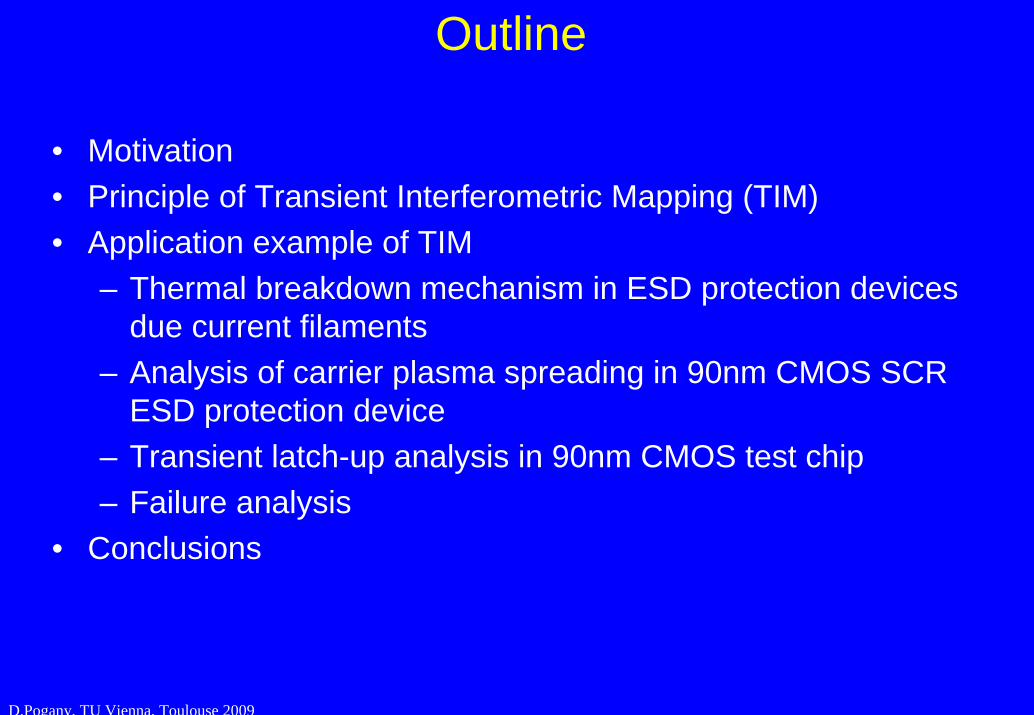
• Motivation• Principle of Transient Interferometric Mapping (TIM)• Application example of TIM
– Thermal breakdown mechanism in ESD protection devices due current filaments
– Analysis of carrier plasma spreading in 90nm CMOS SCR ESD protection device
– Transient latch-up analysis in 90nm CMOS test chip– Failure analysis
• Conclusions
Outline
D.Pogany, TU Vienna, Toulouse 2009
MotivationExperimental access to internal device parameters (temperature, carrier concentration, current density, electric field) is important for:
Finding critical places in devices - hot spots, thermo-mechanical stress,..
Device structure and performance optimization
Verification of simulation resultsCalibration of simulation modelsPrediction of device failure threshold
Thermal and high injection effects important in: power devices, electrostatic discharge (ESD) protection devices, etc...
⇒ TIM method provides µm space and ns time resolution and access to bulk properties from backside
D.Pogany, TU Vienna, Toulouse 2009
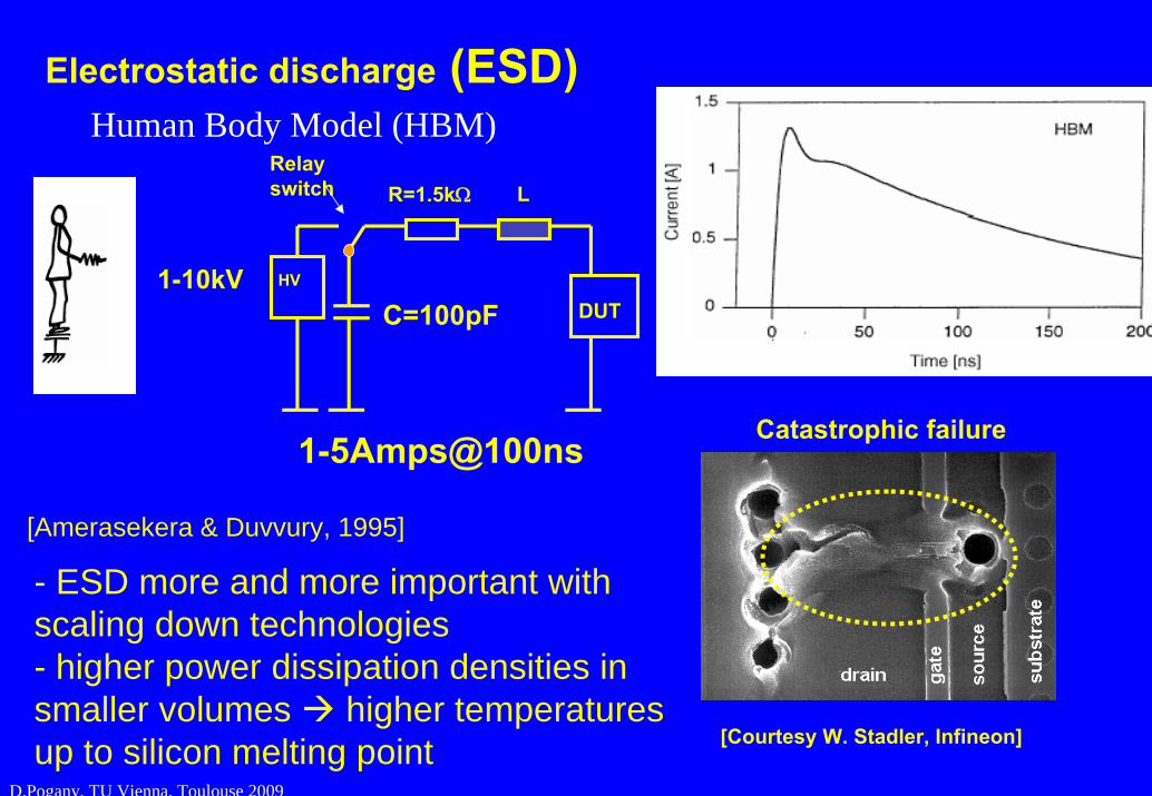
Electrostatic discharge (ESD)Human Body Model (HBM)
1-10kV
1-5Amps@100ns
[Courtesy W. Stadler, Infineon]
Catastrophic failure
HV
Relayswitch R=1.5kΩ
C=100pF
L
DUT
[Amerasekera & Duvvury, 1995]
- ESD more and more important with scaling down technologies- higher power dissipation densities in smaller volumes higher temperaturesup to silicon melting point
D.Pogany, TU Vienna, Toulouse 2009
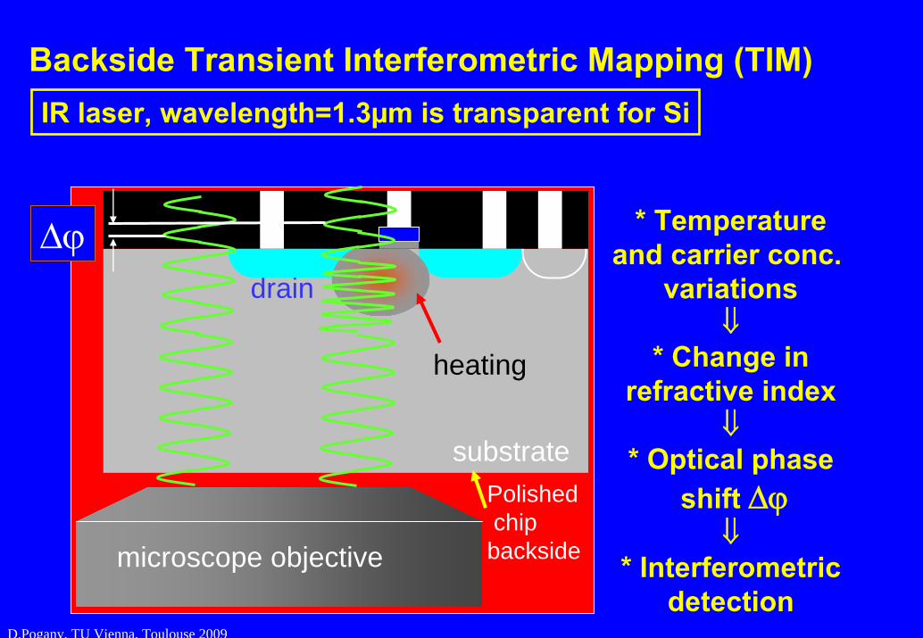
* Temperatureand carrier conc.
variations⇓
* Change inrefractive index
⇓* Optical phase
shift Δϕ⇓
* Interferometricdetection
substrate
drain
Polishedchipbacksidemicroscope objective
gate
heating
Δϕ
Backside Transient Interferometric Mapping (TIM)IR laser, wavelength=1.3µm is transparent for Si

D.Pogany, TU Vienna, Toulouse 2009
General optical principle of TIM
( ) ( ) ( ) ( )[ ]∫ ⎭⎬⎫
⎩⎨⎧ Δα+Δα+Δ
λπ
=ϕΔ dzt,zpt,znt,zTdTdn4t pn
Optical phase shift (integral along the laser path):
Thermal contribution>0
Free-carrier contribution<0
Both components can bedistinguished according to
the sign and different time scales
Thermal component is dominant at high dissipated powers
+
Δϕ
Free-carrier
Temperature
Time
Sum T+FC
[Goldstein &,Rev.Sci. In. 64(1993)3009, D.Pogany & IEEE TED 49(2002)2070]

D.Pogany, TU Vienna, Toulouse 2009
Method is quantitative:
APEX postprocessor of Synopsis allows calculation of phase shift data from the simulated temperature and free carrier distributions of device simulation (TCAD) DESSIS

D.Pogany, TU Vienna, Toulouse 2009
Transient interferometric mapping (TIM) at TU Vienna:
* Scanning heterodyne interferometer + Michelson- 3ns and 1.5µm resolution- phase shift transients recorded at eachscanning position- repetitive stressing necessary forspatial imaging
* 2D holographic interferometric method- 5ns and 3µm resolution - one or two 2D images recorded
per single stress pulse- single event thermal imaging- wafer level probing possible

D.Pogany, TU Vienna, Toulouse 2009
Scanning heterodyne interferometer
IR observationcameramicroscope
objective D.U.T.
AOM
laser diode=1310 nmλ
+ω 1
ω 2 external referencemirror
MOS-switchxy-stage
mirror
photo diode
TLP testervf-TLP testerDMOS pulser
HVsourceHVsource
* 1.5µm space resolution* 3ns time resolution
Spatial distribution:
- periodical device stressing
- lateral device scanning
Focused laser beam used Fürböck &, Microel. Rel. 40(2000)1365]

D.Pogany, TU Vienna, Toulouse 2009
Scanning heterodyne interferometer: signal and phase shiftD
etec
tor s
igna
l
noheating
heatingΔϕ
Heating
0 200 400 600 8000.00.40.81.21.6
Time (ns)
Phas
e sh
ift (r
ad)
Detector signal:
A sin[2Δωt+Δϕ(t)]
* Time domain detection* Automated acquisition* FFT analysis* phase extraction insensitive to sample reflectivity
[Fürböck &, J. Elstat, 49(2000)195]
[M.Litzenberger &, IEEE TIM, 54(2005)2438]
D.Pogany, TU Vienna, Toulouse 2009
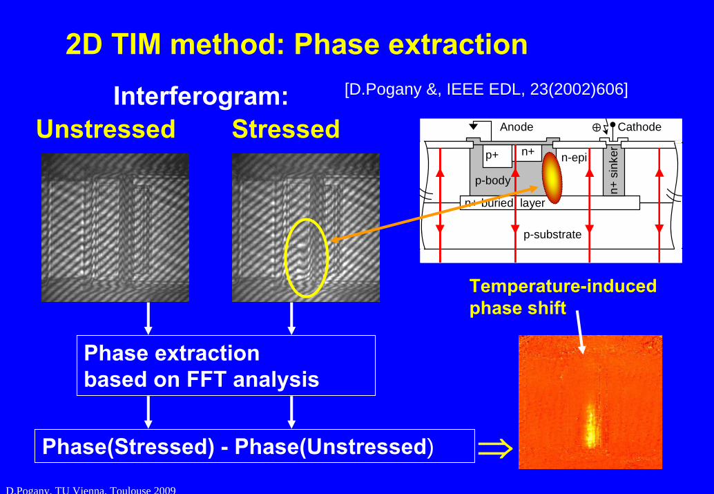
2D TIM method: Phase extraction
Phase extraction based on FFT analysis
Phase(Stressed) - Phase(Unstressed) ⇒
Temperature-inducedphase shift
StressedInterferogram:
Unstressed
p-body
n+ s
inke
r
n+ buried layer
p-substrate
n-epip+ n+
⊕ CathodeAnode
[D.Pogany &, IEEE EDL, 23(2002)606]

D.Pogany, TU Vienna, Toulouse 2009
2D TIM method
DUT
NPBS
IRcamera 2
PC
HVelectron.
pulser
1kΩ
50Ω
OSCIL.
M
Beam 2Electricalsignal path
L
L
MO
Monitor
CT1
DET
Lase
r 1
Laser 2 PBS
IRcamera 1
PBS
Beam 1
Pulsecontrol
• orthogonally polarized laser beams
• laser pulse duration 5ns
• relative laser pulse delay 0 ns - 5 μs
• phase distribution at two time instants during single stress pulse
- non-repetitive phenomena (destructive)
[Dubec &, Microel.Reliab. 44(2004)1793]
Imaging at two time instants during a single shot

D.Pogany, TU Vienna, Toulouse 2009
Model verification at high temperatures by TIM
[S. Reggiani et al. I3E EDL, vol.26 2005, p.916]
Up to 1100K models for impact ion. coeff. verified experimentally
ESD protection diode : comparisom TIM vs. TCAD simulation

D.Pogany, TU Vienna, Toulouse 2009
4 rad-1 rad
130 ns
530 ns
290 ns
200 ns Filament moves to left
Filament has been created
Filament reflects from device corner
Filament moves back
130 ns
530 ns
290 ns
200 ns
30 mW/μm2-30
P2D – extracted power density
Phase shift –measured
[Dubec &, Microel.Reliab. 44(2004)1793]
Current filament dynamics in ESD protection devices
p-body
n+ s
inke
r
n+ buried layer
p-substrate
n-epip+ n+
⊕ CathodeAnode

D.Pogany, TU Vienna, Toulouse 2009
Instantaneous power extraction from TIM measurements
Filament movement along the device width
Measured: Δϕ: memory effect
Calculated:
P2D ≈
curr.
density
By 2D scanning
Device width
p - substrate
n+ buried layer
p body
p+n+sinker
n- epi
+
laser beam
anode cathode
n+
Iav
Npn ESD prot. device
[Pogany &, App.Phys.Lett,81(2002)2881]
Dev
ice
leng
th
Device length
Device
widt
h
D.Pogany, TU Vienna, Toulouse 2009
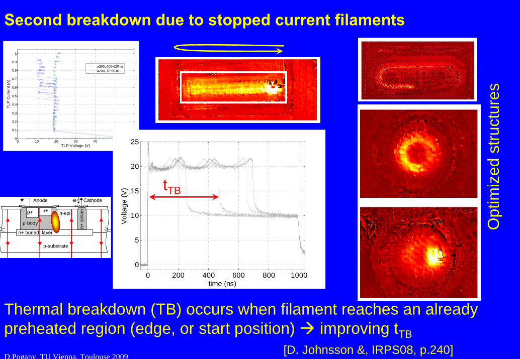
Second breakdown due to stopped current filaments
[D. Johnsson &, IRPS08, p.240]
Thermal breakdown (TB) occurs when filament reaches an already preheated region (edge, or start position) improving tTB
0 10 20 30 40 50 600
0.1
0.2
0.3
0.4
0.5
0.6
0.7
0.8
0.9
1
TLP Voltage (V)
TLP
Cur
rent
(A)
w200, 600-620 nsw200, 70-90 ns
0 200 400 600 800 10000
5
10
15
20
25
Vol
tage
(V)
time (ns)
p-body
n+ s
inke
r
n+ buried layer
p-substrate
n-epip+ n+
⊕ CathodeAnode
Opt
imiz
ed s
truct
ures
tTB

D.Pogany, TU Vienna, Toulouse 2009
TLU analysis in 90nm CMOS structures
0µs 1µs 2µs 3µs0V
3V D
etec
tor V
olta
ge
0µs 1µs 2µs 3µs
-50
0
Pha
se [m
rad]
Laser[K.Domanski et al. EOS/ESD’07, p.347]
* Invertor sensitivity to Latch –up is studued* Injector diode emulates substrate current injection
D.Pogany, TU Vienna, Toulouse 2009
TU-Wien
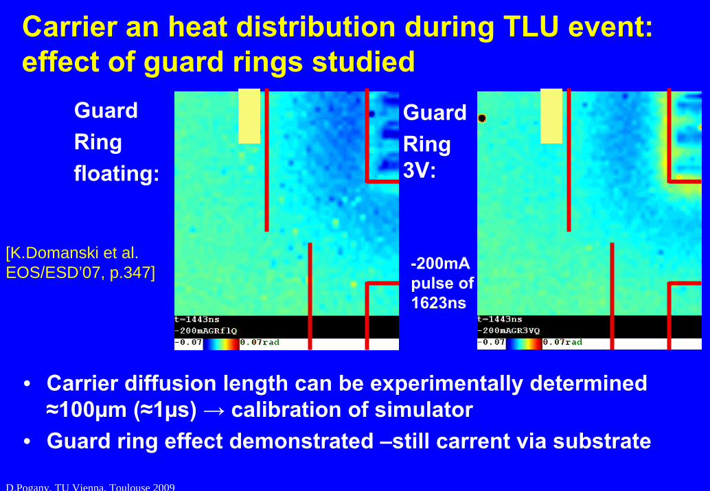
Carrier an heat distribution during TLU event: effect of guard rings studied
• Carrier diffusion length can be experimentally determined ≈100µm (≈1µs) → calibration of simulator
• Guard ring effect demonstrated –still carrent via substrate
GuardRingfloating:
GuardRing 3V:
-200mA pulse of 1623ns
[K.Domanski et al. EOS/ESD’07, p.347]

D.Pogany, TU Vienna, Toulouse 2009
N-well
P-well, P-substrate
p+
p+
p+
n+
n+
n+
Z
Y
t1
t1: t2: t3:
t2 >t1
t3 >t2
J1 J2<J1 J3<J2
Density of current inside filament
90 nm CMOS SCR study: spreading of the on state
-electron-hole plasma spreads with time to sides and to substrate- heating follows with a delay the current flow
[K.Esmark et al, IRPS08, p.247]

D.Pogany, TU Vienna, Toulouse 2009
ESD failure detection using 2D TIM method – rough position detection in a large field of view
2 mW ~ 3 mrad FOV 1.6x1.3 mm
FOV 3x2.5 mmIR image Interferogram difference
2 mW ~ 3 mrad
[V.Dubec et al. , Microel. Reliab, 47(2007)1549]Testing on npn transistor
IR image Interferogram difference
Stroboscopic detection usingrepetitive pulses +stabizedMichelson interferometer

D.Pogany, TU Vienna, Toulouse 2009
Scanning TIM technique for failure analysis- metal short detection
• power resolution up to 50 μW• spatial resolution 2 μm• comparable to standard FA methods (e.g. TIVA)•possible to combine FA with standard TIM for ESD analysis
AOM
DUT
DET + L.O. = Phase
ω ω+Ω1 ω+Ω2
Ω1t - Ω2t + Δϕ Ω1t - Ω2t Δϕ
LaserMicroscope
IR image
-800 -600 -400 -200 0 200
0.0
0.1
0.2
0.3
0.4
Pha
se (r
ad)
X-position (μm)
Single beam scanDifferential scan
2D scan
Scan area1x1 mm
(metal short)
[V.Dubec et al. , Microel. Reliab, 47(2007)1549]

D.Pogany, TU Vienna, Toulouse 2009
Conclusions
TIM :
– free carrier and thermal dynamics can be detected with ns time and µm space resolution
– understanding device physics and for device layout optimisation
- used for calibration and verification of device simulation models under high current and high temperature conditions
- failure analysis application
- other applications include thermal mapping of GaN HEMTs, lasers [J.Kuzmik &, APL 2003, IEEE TED 2005, SSE 2006,…]
Recommended