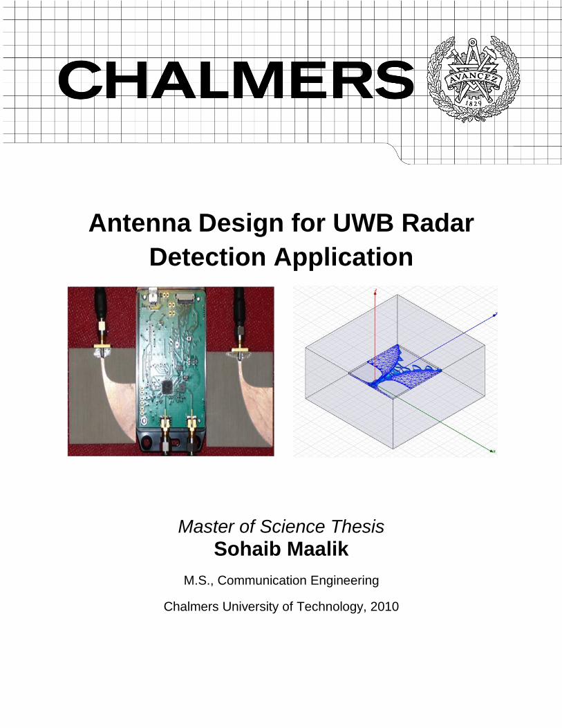
Antenna Design for UWB Radar
Detection Application
Master of Science Thesis
Sohaib Maalik
M.S., Communication Engineering
Chalmers University of Technology, 2010
II
Thesis Supervisors: Jian Yang Docent, Chalmers university of technology
Kenneth Malmström Project Manager, System Design Imego, AB
Lars Landén Research scientist, System Design Imego, AB
Examiner: Dr.Jian Yang Chalmers University of Technology Antenna Group, Department of Signals and Systems SE-412 96 Goteborg Sweden Tel: +46 31 7721736
III
ABSTRACT This master thesis has focused on the aspect of UWB antenna design for the impulse
based UWB radar which is built on CMOS technology. The design of new UWB antenna
faces some challenges. The antenna should be compact, preferably conformal, low cost
for manufacture, and have good electrical performance, such as good matching,
directional radiation performance over a wide band, good time response, etc. Keeping
these goals in mind a compact and directional antipodal Vivaldi antenna was built. The
antenna radiating structure is in the form of two exponentially tapered arms that lie on
the opposite sides of the substrate. The antenna operates over the frequency band from
2.7 GHz to more than 12 GHz. It exhibits a directive radiation performance with a peak
gain which is between 3.2dBi and 10.2dBi in the specified band. The time domain
performance of the antenna shows negligible distortion of the pulse which makes it
suitable to use with impulse based UWB radar. The antenna has linear phase response
over the entire UWB frequency range and hence constant group delay which is vital for
transmission and reception of sub-nanosecond pulses. Due to its planar profile,
physically compact size, wide impedance bandwidth, directive performance over a wide
bandwidth antipodal Vivaldi antenna is a good candidate for use with Novelda UWB
radar chip and other UWB integrated circuits and portable electronics. The antenna is
being used for ranging, one and two dimensional tracking along with Novelda R2A UWB
radar chip.
IV
Acknowledgements First and foremost, thanks to God Almighty who gave me courage and strength to complete this project. I would like to thank my supervisor Docent Jian Yang at Chalmers University of technology for his constant support and guidance throughout the thesis work. Without him this project would not be possible. I would also like to express the deepest gratitude to my supervisor Kenneth Malmström at Imego AB, for believing in me and giving me the opportunity to work on this project. He gave me free hand and made me feel at home at Imego. I am gratefully thankful to Lars Landen and Dimitar Kolev for their continuous help and suggestions whenever I needed it, especially Dimitar without whom antenna fabrication was not possible. In the end special thanks to Lars for reviewing the thesis report and giving valuable suggestions to improve it. I would also like to thank the pillars of my life that kept supporting me unconditionally throughout my life up till now, my beloved parents.

V
Table of Contents
ABSTRACT ................................................................................................................................................ III
Acknowledgements ................................................................................................................................... IV
List of Figures ........................................................................................................................................... VII
List of Tables ............................................................................................................................................ VIII
List of Abbreviations.................................................................................................................................. IX
Chapter 1 ..................................................................................................................................................... 1
INTRODUCTION ........................................................................................................................................ 1
1.1 History and Background ..................................................................................................................... 3
1.2 Thesis Objective .................................................................................................................................. 3
1.2 Organization of the Report ................................................................................................................. 4
Chapter 2 ..................................................................................................................................................... 5
UWB CMOS Radar Chip ........................................................................................................................... 5
2.1- Impulse Radar..................................................................................................................................... 5
2.2- Novelda R2A ....................................................................................................................................... 6
2.2.1- The Chip Architecture ................................................................................................................. 6
2.2.2- Basic parameters of Novelda Radar ........................................................................................ 8
2.2.3- Basic principle of Novelda Radar ............................................................................................. 9
Chapter 3 ................................................................................................................................................... 10
Antenna Theory ........................................................................................................................................ 10
3.1 Antenna Characteristics ................................................................................................................... 10
3.1.1 Directivity ..................................................................................................................................... 10
3.1.2 Gain .............................................................................................................................................. 10
3.1.3 Reflection Coefficient ................................................................................................................. 11
3.1.4 Radiation pattern ........................................................................................................................ 11
3.2 UWB antenna requirements ............................................................................................................. 12
Chapter 4 ................................................................................................................................................... 13
Antenna Design ........................................................................................................................................ 13
4.1- The Antipodal Vivaldi antenna........................................................................................................ 13
4.1.1-Antenna Geometry ..................................................................................................................... 14
4.1.2-Parallel strip line to microstrip transition ................................................................................. 15
VI
4.1.3- Principle of operation ................................................................................................................ 16
4.2- Results and discussion .................................................................................................................... 17
4.2.1- Reflection coefficient S11 ........................................................................................................ 17
4.2.2- Phase Response ....................................................................................................................... 17
4.2.3- Group Delay ............................................................................................................................... 18
4.2.4- Gain ............................................................................................................................................. 20
4.2.5- Radiation patterns ..................................................................................................................... 23
4.2.6- Summary .................................................................................................................................... 27
Chapter 5 ................................................................................................................................................... 29
Conclusions and future work .................................................................................................................. 29
5.1- Conclusions ....................................................................................................................................... 29
5.2- Future work ....................................................................................................................................... 29
References ................................................................................................................................................ 31
VII
List of Figures Figure 1- Diagram explaining the difference between a signal compressed in time domain to the
one expanded in time domain .................................................................................................................. 1
Figure 2- The FCC spectral mask for Indoor Unlicensed UWB emission [1] .................................... 2
Figure 3-The NVA 3000 UWB radar chip on PCB ................................................................................ 6
Figure4- Gaussian pulse from the pulse generator with center frequency 4.3 GHz seen in time
domain with amplitude in volts [11] ........................................................................................................ 7
Figure 5- Gaussian pulse from the pulse generator with center frequency 4.3 GHz seen in
frequency domain together with the limit values set by FCC [11] ....................................................... 7
Figure 6- Illustration of the Novelda radar basic function ..................................................................... 9
Figure 7- Top View of antipodal Vivaldi antenna modeled in HFSS [10] ......................................... 14
Figure 8- Parallel strip line to microstrip transition .............................................................................. 15
Figure 9- Fabricated antipodal Vivaldi antenna ................................................................................... 16
Figure 10- Measured and simulated Reflection coefficient ............................................ 17
Figure 11- Measured Phase response of antenna .............................................................................. 18
Figure 12-The Group Delay measurement setup for Antipodal Vivaldi antenna in Chase group
Lab at Chalmers ....................................................................................................................................... 19
Figure 13- Group Delay vs Frequency for antipodal Vivaldi antenna .............................................. 20
Figure 14- The standard-gain Horn antennas used as reference for gain measurement ............. 21
Figure 15- Gain measurement done in anechoic chamber at Chase group, Chalmers ................ 22
Figure 16- Simulated and measured gain for the antipodal Vivaldi antenna .................................. 23
Figure 17- Radiation Pattern measurement setup .............................................................................. 24
Figure 18- Normalized E-Plane and H-Plane radiation patterns at 4 GHz ...................................... 25
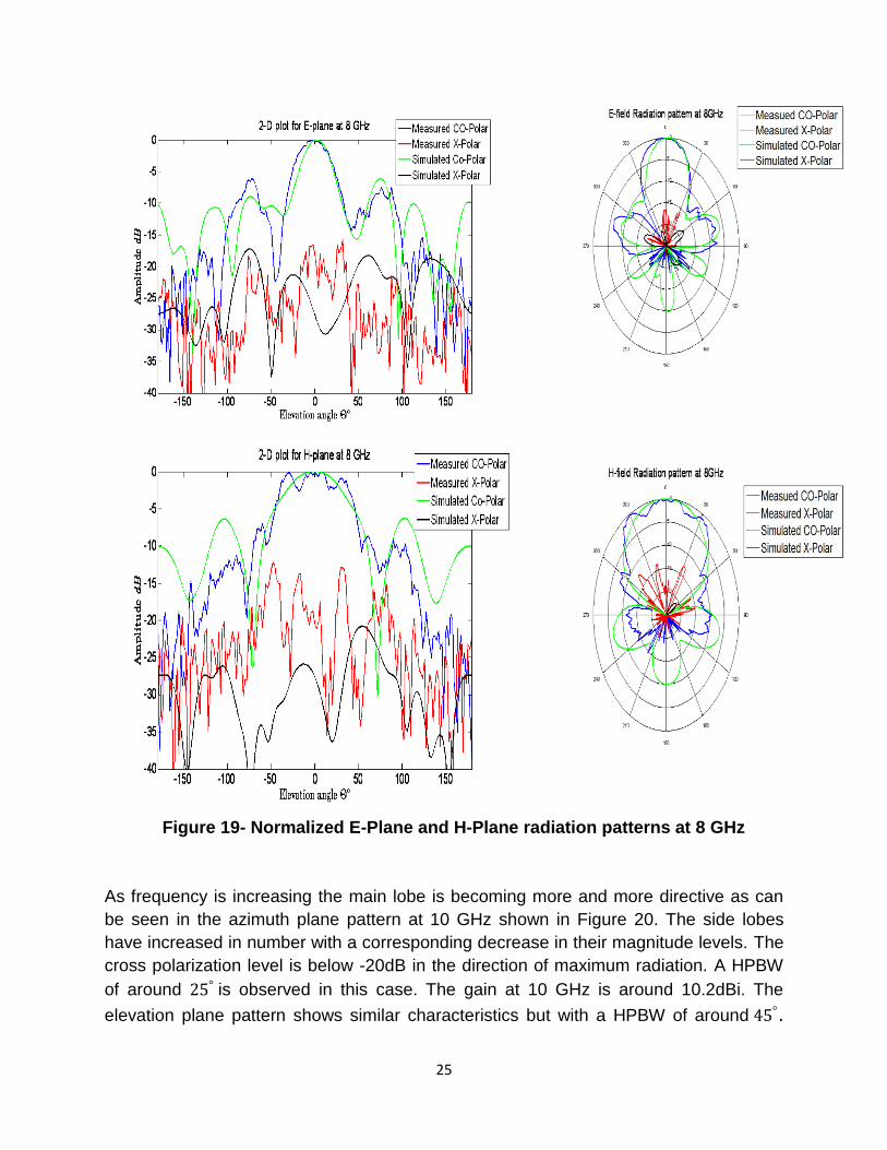
Figure 19- Normalized E-Plane and H-Plane radiation patterns at 8 GHz ...................................... 25
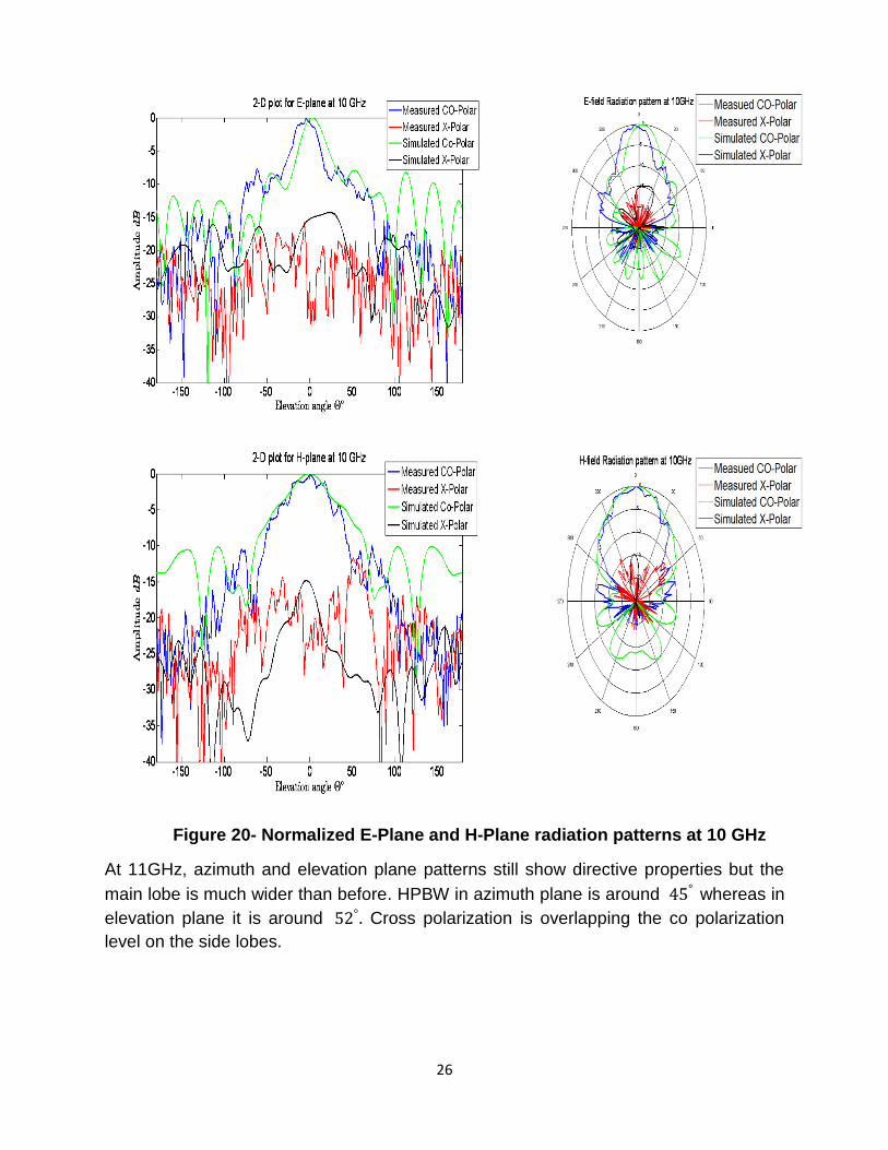
Figure 20- Normalized E-Plane and H-Plane radiation patterns at 10 GHz ................................... 26
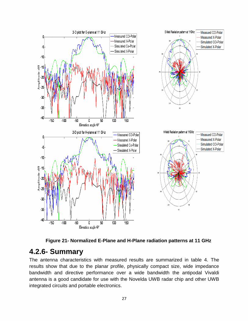
Figure 21- Normalized E-Plane and H-Plane radiation patterns at 11 GHz ................................... 27
Figure 22- Complete system for object detection ................................................................................ 29
VIII
List of Tables Table1- Important parameters of UWB radar chip and their functionalities ..................... 8
Table 2- UWB Antenna design requirements for Novelda R2A Radar transceiver ........ 12
Table 3- Design parameters for antipodal Vivaldi antenna ............................................ 16
Table 4- Antenna results summary ............................................................................... 28
IX
List of Abbreviations
Abbreviation Description
APVA
Antipodal Vivaldi Antenna
AUT
Antenna Under Test
FCC
Federal Communications Commission
GS/s
GigaSamples/Second
HFSS
High Frequency Structure Simulator
HPBW
Half Power Beam Width
PC
Personal Computer
PCB
Printed Circuit Board
PMC
Perfect Magnetic Conductor
SGH
Standard-Gain Horn Antenna
USB
Universal Serial Bus
UWB
Ultra-WideBand
VNA
Vector Network Analyzer
1
Chapter 1
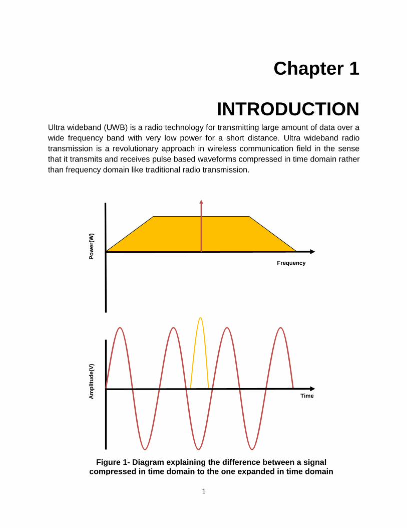
INTRODUCTION Ultra wideband (UWB) is a radio technology for transmitting large amount of data over a
wide frequency band with very low power for a short distance. Ultra wideband radio
transmission is a revolutionary approach in wireless communication field in the sense
that it transmits and receives pulse based waveforms compressed in time domain rather
than frequency domain like traditional radio transmission.
Time Am
pli
tud
e(V
)
Frequency
Po
we
r(W
)
Figure 1- Diagram explaining the difference between a signal compressed in time domain to the one expanded in time domain
2
Figure 1 explains the difference between a traditional narrow band system which usually
uses periodic sinusoidal signal (expanded in time domain) for communication to an
UWB system which uses narrow time domain pulse which spans over a very wide
frequency band.
In February 2004, Federal communications commission (FCC) allocates unlicensed
frequency band of 3.1-10.6 GHz for UWB applications. The allocation of unlicensed
spectrum to UWB technology generated a lot of interest in industry and opened the
doors for development of numerous daily life applications based on UWB technology.
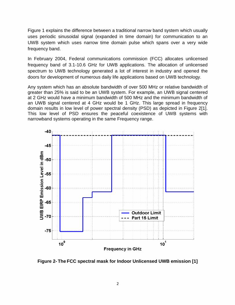
Any system which has an absolute bandwidth of over 500 MHz or relative bandwidth of greater than 25% is said to be an UWB system. For example, an UWB signal centered at 2 GHz would have a minimum bandwidth of 500 MHz and the minimum bandwidth of an UWB signal centered at 4 GHz would be 1 GHz. This large spread in frequency domain results in low level of power spectral density (PSD) as depicted in Figure 2[1]. This low level of PSD ensures the peaceful coexistence of UWB systems with narrowband systems operating in the same Frequency range.
Figure 2- The FCC spectral mask for Indoor Unlicensed UWB emission [1]
3
1.1 History and Background The term „Ultra-wideband‟ has several similar meanings such as impulse, carrier-free,
baseband, and large relative bandwidth radio or radar signals. The concept of Ultra-
wideband technology is not new. The first pulse-based UWB spark Gap radio was
developed by Guglielmo Marconi in the late 1800 which was used to transmit Morse
code for several years. However, in early 1900, these radios were forbidden to use in
many applications due to their strong power emission and interference with other
narrow band radio systems, which were developed in early 1900,s [2,3].
In the late 1960,s UWB technology gained a lot of interest because of its use in the form
of impulse radar in military area. During this era significant research efforts were
conducted by researchers on different aspects of Ultra-wideband technology. In 1964
Hewlett Packard and Tektronix Inc. produced the first time domain instruments for sub-
nanosecond pulse diagnostics which was a huge step in UWB system design. Antenna
designers such as Rumsey, Dyson and Ross have started the design of antennas for
UWB systems. Rumsey and Dyson developed logarithmic spiral antennas [4, 5] and
Ross used impulse measurement techniques for the design of wideband radiating
antenna elements [6]. During 1960 to 1999, nearly a 40 year period, over 200 papers
were published in accredited IEEE journals, and more than 100 patents were issued on
topics related to UWB technology [7]. With these advances in the UWB field the
potential of using impulse based UWB technology for radar and communication became
clear.
At the beginning of 2002 UWB was reborn after FCC approved the UWB technology for
commercial use. UWB systems have a number of advantages over traditional
narrowband systems which makes it more suitable for a variety of applications including
radar measurements in the time domain. UWB systems have potentially low complexity,
low cost and more importantly they have a very good time domain resolution [8].
Attributes such as low power consumption, negligible interference to narrowband
systems, inherent immunity against detection and interception, strong penetration ability
through different materials etc makes UWB technology a good candidate for through-
the-wall and ground penetrating applications. This short-range, high-throughput wireless
technology can transmit with data rates of 252 Mbps, and data rate of 480 Mbps is
expected to be achieved in near future [9].
1.2 Thesis Objective This thesis represents a continuation of the previous work done in the UWB Radar
application project at Imego AB, which has long experience in the field of sensor
technology. The Imego UWB radar application project was started in January 2008 and
is based on the Novelda AS R2A CMOS radar chips. The antenna is an integral part of
4
any UWB radar application. Therefore, previously a planar, broadband and directional
Vivaldi antenna has been developed to work with the Novelda AS R2A radar chips. Two
prototypes of the Vivaldi antenna have been developed. One chip covers the low
frequency range and operates from 900MHz to 5GHz whereas the higher frequency
chip covers the UWB range from 5GHZ to 8GHz. Prototype Vivaldi 004(150mm ×
132mm) operates over the lower frequency band and Vivaldi005 (60mm × 46mm)
operates in the higher frequency band.
The prime focus of this Thesis is to design an antenna which is operable over the entire
UWB frequency range. The antenna should be physically compact, planar and have low
manufacturing cost as well. Furthermore the antenna should exhibit good electrical
performance such as good impedance matching, directional radiation performance over
the entire UWB range and most importantly it should have a good time response which
is very vital in order to successfully transmit and receive sub nanosecond pulses. The
antenna has to be directive enough so that it can be used with the Novelda AS R2A
radar chips to develop one and two dimensional motion tracking applications.
1.2 Organization of the Report In Chapter 2 the Novelda AS R2A radar chip is discussed in detail. The chapter starts
with the history of impulse radars and then the Novelda NVA3000 radar chip is
introduced. The Basic principle of the Novelda radar and later on the Novelda radar chip
architecture is explained. The fundamental parameters to control the radar chips are
also discussed.
Chapter 3 belongs to antenna theory. It includes the definition of the fundamental
parameters of the antenna such as gain, directivity, return loss, impedance bandwidth
and radiation pattern. The requirements, limitations and challenges in the design of
UWB antennas are also discussed.
In addition, a directional antipodal Vivaldi antenna (APVA) is presented in chapter 4.
Antipodal Vivaldi antennas are well known in literature due to their wide impedance
bandwidth and directional radiation properties. The antenna is modeled and simulated
using HFSS [10]. The results show that the antipodal Vivaldi antenna has a good
impedance matching, well more than the entire UWB range. Furthermore, the antipodal
Vivaldi antenna has much smaller size than previously developed Vivaldi antennas.
Simulated and measured radiation patterns confirm good directional radiation
performance over the entire UWB range. All the measured results and their comparison
with simulated results are also presented.
In Chapter 5, brief description of some of the possible applications and suggestions for
future work are discussed.
5
Chapter 2
UWB CMOS Radar Chip The Basic principle of the radar, short for “Radio Detection And Ranging”, has been the same since the German physicist Heinrich Hertz in the late 19th century discovered that electromagnetic waves have the ability to reflect off surfaces. Radar works by transmitting electromagnetic waves towards an object, and then receiving the energy reflected by the object. However, it was not until the early 20th century that systems able to use these principles were developed. Systems capable of measuring the time it takes for a transmitted electromagnetic signal to travel between the antenna and the reflecting object was developed during the first part of the 20th century, and in 1940 the term radar was coined by the U.S. Navy [11].
2.1- Impulse Radar Radar technology has progressed significantly since world war two (WWII). An Impulse
Radar is a device that can sense the distance to one or more remote objects by emitting
and receiving very short pulses of electromagnetic energy [11]. As pulse radars were
initially being developed, the use of very narrow pulses was examined. In the early
days, the electronics for generating and receiving such narrow pulses were not
available; thus, essentially no applications of this were initially made. By the 1970s,
advances in electronics and high speeds in modern integrated circuits made it possible
to transmit extremely short electromagnetic pulses thus paving the way to develop
impulse based UWB systems. Unique attributes such as high penetration abilities, very
high accuracy and low emission levels give such system an edge over traditional
narrowband systems.
Today, impulse based UWB radar transceivers are becoming available on the market.
One such UWB radar transceiver has been developed by a Norwegian company,
Novelda [11]. In this thesis project, the Novelda NVA3000 UWB radar chip has been
used which is based on CMOS technology. This UWB radar chipset has been selected
as it is considered to have a low cost of production on a large scale in comparison with
other similar products on the market. It is important to understand how this UWB radar
chipset works in order to design practical UWB radar antennas that can be used along
with this chipset developing different applications.
6
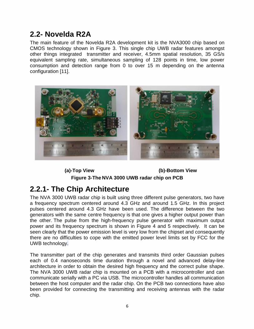
2.2- Novelda R2A The main feature of the Novelda R2A development kit is the NVA3000 chip based on CMOS technology shown in Figure 3. This single chip UWB radar features amongst other things integrated transmitter and receiver, 4.5mm spatial resolution, 35 GS/s equivalent sampling rate, simultaneous sampling of 128 points in time, low power consumption and detection range from 0 to over 15 m depending on the antenna configuration [11].
Figure 3-The NVA 3000 UWB radar chip on PCB
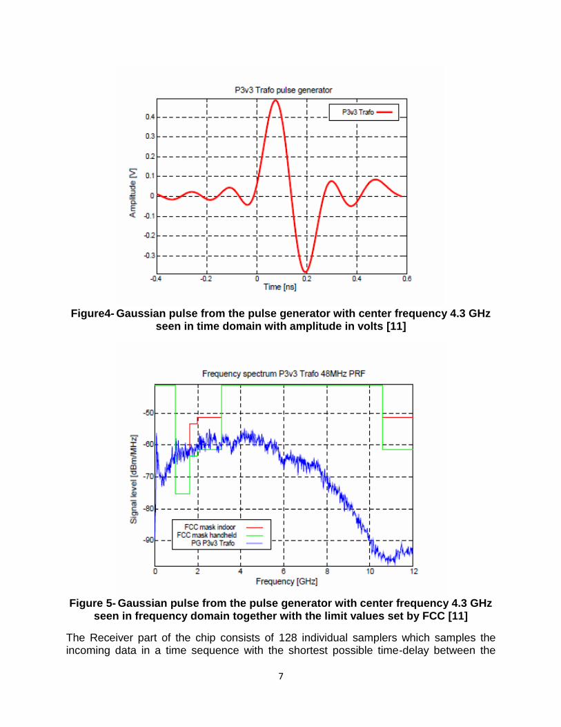
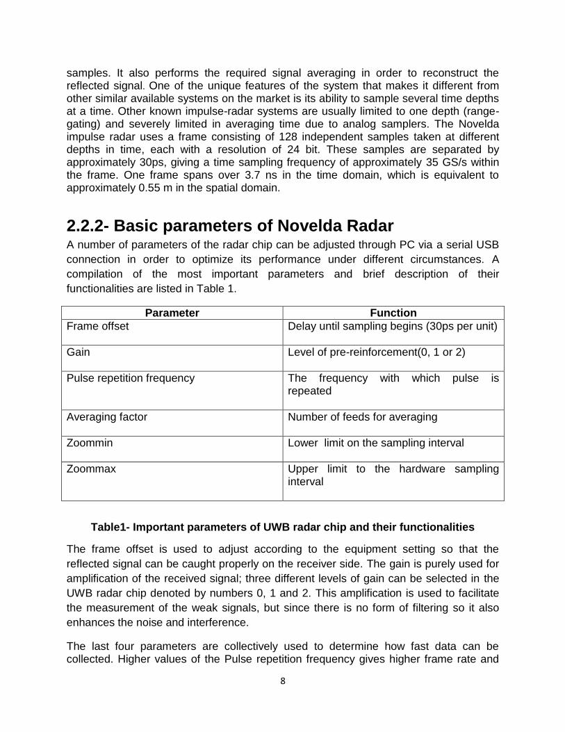
2.2.1- The Chip Architecture The NVA 3000 UWB radar chip is built using three different pulse generators, two have a frequency spectrum centered around 4.3 GHz and around 1.5 GHz. In this project pulses centered around 4.3 GHz have been used. The difference between the two generators with the same centre frequency is that one gives a higher output power than the other. The pulse from the high-frequency pulse generator with maximum output power and its frequency spectrum is shown in Figure 4 and 5 respectively. It can be seen clearly that the power emission level is very low from the chipset and consequently there are no difficulties to cope with the emitted power level limits set by FCC for the UWB technology. The transmitter part of the chip generates and transmits third order Gaussian pulses each of 0.4 nanoseconds time duration through a novel and advanced delay-line architecture in order to obtain the desired high frequency and the correct pulse shape. The NVA 3000 UWB radar chip is mounted on a PCB with a microcontroller and can communicate serially with a PC via USB. The microcontroller handles all communication between the host computer and the radar chip. On the PCB two connections have also been provided for connecting the transmitting and receiving antennas with the radar chip.
(a)-Top View (b)-Bottom View
7
Figure4- Gaussian pulse from the pulse generator with center frequency 4.3 GHz
seen in time domain with amplitude in volts [11]
Figure 5- Gaussian pulse from the pulse generator with center frequency 4.3 GHz
seen in frequency domain together with the limit values set by FCC [11]
The Receiver part of the chip consists of 128 individual samplers which samples the incoming data in a time sequence with the shortest possible time-delay between the
8
samples. It also performs the required signal averaging in order to reconstruct the reflected signal. One of the unique features of the system that makes it different from other similar available systems on the market is its ability to sample several time depths at a time. Other known impulse-radar systems are usually limited to one depth (range-gating) and severely limited in averaging time due to analog samplers. The Novelda impulse radar uses a frame consisting of 128 independent samples taken at different depths in time, each with a resolution of 24 bit. These samples are separated by approximately 30ps, giving a time sampling frequency of approximately 35 GS/s within the frame. One frame spans over 3.7 ns in the time domain, which is equivalent to approximately 0.55 m in the spatial domain.
2.2.2- Basic parameters of Novelda Radar A number of parameters of the radar chip can be adjusted through PC via a serial USB
connection in order to optimize its performance under different circumstances. A
compilation of the most important parameters and brief description of their
functionalities are listed in Table 1.
Parameter Function
Frame offset
Delay until sampling begins (30ps per unit)
Gain
Level of pre-reinforcement(0, 1 or 2)
Pulse repetition frequency
The frequency with which pulse is repeated
Averaging factor
Number of feeds for averaging
Zoommin
Lower limit on the sampling interval
Zoommax Upper limit to the hardware sampling interval
Table1- Important parameters of UWB radar chip and their functionalities
The frame offset is used to adjust according to the equipment setting so that the
reflected signal can be caught properly on the receiver side. The gain is purely used for
amplification of the received signal; three different levels of gain can be selected in the
UWB radar chip denoted by numbers 0, 1 and 2. This amplification is used to facilitate
the measurement of the weak signals, but since there is no form of filtering so it also
enhances the noise and interference.
The last four parameters are collectively used to determine how fast data can be collected. Higher values of the Pulse repetition frequency gives higher frame rate and
9
vice versa. The Averaging Factor determines how many times the signal is averaged at the radar chip. Increasing the averaging factor will lower the frame rate but increase the signal to noise ratio. Useful values for averaging factor are approximately 1000 to 25,000. Zoom range determines the maximum and minimum value to sample at the receiver. The zoom values are 24 bit integers and can be set to anything between 0 and 16777215.
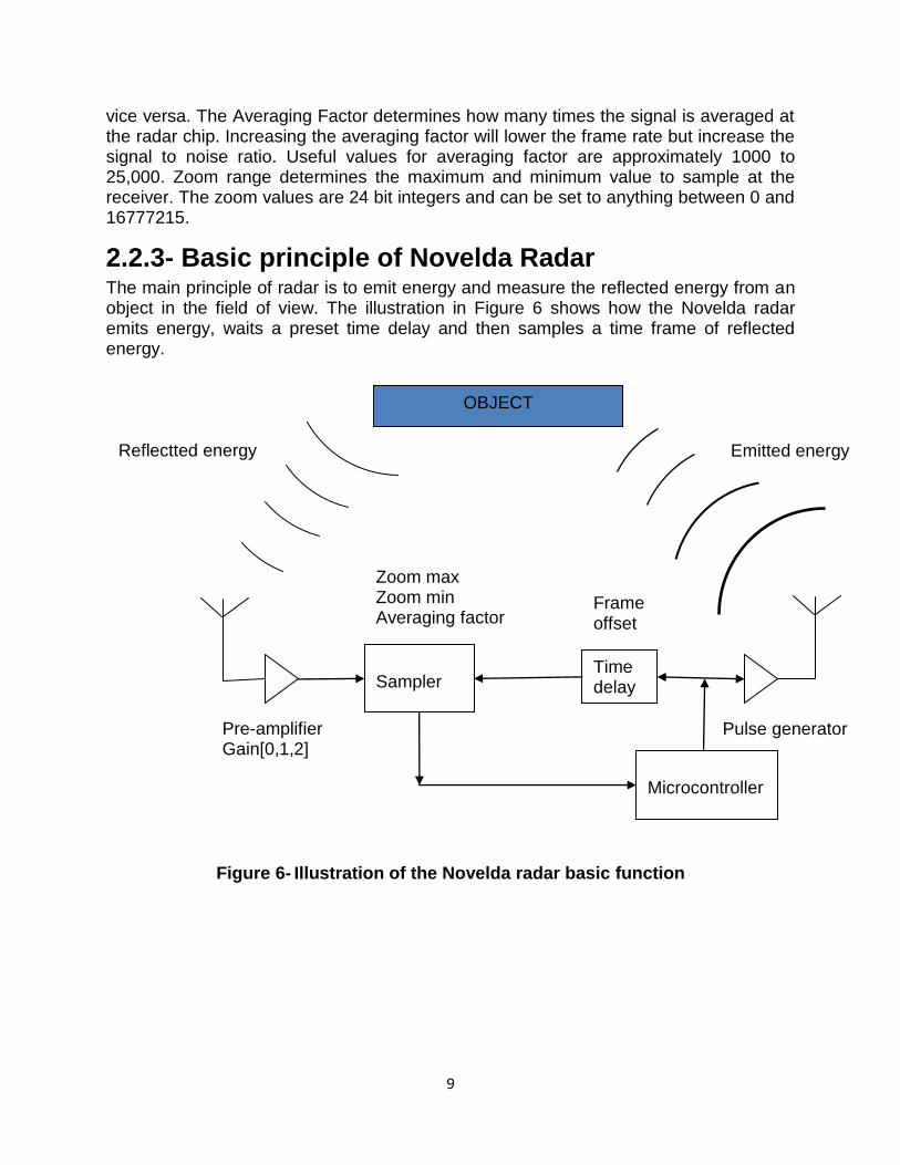
2.2.3- Basic principle of Novelda Radar The main principle of radar is to emit energy and measure the reflected energy from an object in the field of view. The illustration in Figure 6 shows how the Novelda radar emits energy, waits a preset time delay and then samples a time frame of reflected energy.
Figure 6- Illustration of the Novelda radar basic function
OBJECT
Sampler
Time delay
Microcontroller
Pre-amplifier Gain[0,1,2]
Zoom max Zoom min Averaging factor
Frame offset
Pulse generator
Emitted energy
Reflectted energy
10
Chapter 3
Antenna Theory The antenna is an integral part of any radar system. According to the IEEE standard definitions of terms for antennas (IEEE std 145-1983) an antenna is defined as “a means for radiating or receiving radio waves” [12].The basic role of the radar antenna is to provide a transducer between the free-space propagation and the guided-wave propagation of electromagnetic waves [13]. The antenna directs the radiated energy in the desired direction towards the target so that it can be illuminated. The energy contained in the reflected echo signals is then collected by the antenna and delivered to the receiver. For the Novelda UWB radar chip two antennas are required for transmission and reception of the signal. Due to the reciprocal behavior of antennas, however, only one design is needed for both ports. Any antenna is characterized by several parameters. A brief description of some of these important parameters is given below so that requirements and challenges in designing UWB radar antenna could be understood better.
3.1 Antenna Characteristics
3.1.1 Directivity According to IEEE standard definitions of terms for antennas (IEEE-1983) the directivity
of an antenna is defined as “The ratio of radiation intensity in a given direction from the
antenna to the radiation intensity averaged over all directions. The average radiation
intensity is equal to the total power radiated by the antenna divided by . If the
direction is not specified the direction of maximum radiation intensity is implied” [12].
Mathematically,
Directivity simply gives us an idea that how well radiated energy from an antenna is
transmitted in a specific direction. Definition of directivity does not involve any
dissipative losses in the antenna but only the concentration of radiated power.
3.1.2 Gain A useful parameter to describe the performance of an antenna is the gain. Gain is
closely related to the directivity but it takes into account the efficiency of an antenna as
well as its directional capabilities whereas directivity only describes the directional
11
properties of the antenna. Gain of an antenna is defined as “The ratio of the intensity, in
a given direction, to the radiation intensity that would be obtained if the power accepted
by the antenna were radiated isotropically” [12]. Mathematically,
In most cases we deal with relative gain, which is defined as “The ratio of the power
gain in a given direction to the power gain of a reference antenna in its referenced
direction” [12]. The power input should be the same for both antennas. The reference
antenna can be a dipole, horn or any other antenna whose gain is already calculated or
known. If an application requires a highly directive antenna then gain can be used to
determine the quality of the antenna since gain is linearly proportional to the directivity,
the gain measurement is a direct indication how well directive an antenna is.
3.1.3 Reflection Coefficient
The Reflection coefficient S11 indicates how well an antenna is matched to the input
transmission line. It is a parameter that determines how well signal transition from the
input transmission line to the free space is performed by the antenna. An antenna is
said to be sufficiently matched if 10% or less of the incident signal is lost during this
transition process. The frequency range over which the antenna reflection coefficient
S11 is -10dB or less is said to be the impedance bandwidth of the antenna. Over this
bandwidth it can be operated with minimum power reflection and maximum radiation.
3.1.4 Radiation pattern
An antenna radiation pattern or antenna pattern is defined as “a mathematical function
or a graphical representation of the radiation properties of the antenna as a function of
space coordinates” [12]. The Radiation pattern is measured in the far-field region in
most cases and radiation properties include power flux density, radiation intensity, field
strength, directivity, phase or polarization [12]. The most important radiation property,
however, is the spatial distribution of radiated energy as a function of the observer‟s
position along a path or surface of constant radius. Usually two types of radiation
patterns are used to characterize the radiated power in the far-field sphere surrounding
the antenna. Field pattern which plots the magnitude of electric or magnetic field as a
function of the angular space and power pattern which plots square of the magnitude of
electric or magnetic field as a function of angular space.
In order to have the full picture of radiation pattern of an antenna we have to measure
the E-plane and H-plane patterns. The E-plane contains the electric field (E-field) vector
and the direction of maximum radiation. The magnetic field or H-plane lies at a right
angle to the E-plane and contains the magnetic field (H-field) vector and direction of
12
maximum radiation. Radiation pattern distribution depends on the application for which
an antenna will be used. For example, in the case of mobile communication
omnidirectional antennas are used for which uniformly distributed radiation pattern
around the antenna is desired. However, in the case of radar applications directional
antennas are preferred.
3.2 UWB antenna requirements The primary goal of this project work is to develop a planar, directional and physically
compact UWB antenna for Novelda R2A UWB radar chip. The antenna is developed
keeping in mind a broad range of possible applications that can be achieved using this
impulse based UWB radar transceiver.
In addition to the parameters described above, the UWB antenna design faces some
additional challenges as compared to other narrowband and wideband antennas. By
definition, an Ultra Wideband antenna must be operable over the entire 3.1-10.6
frequency range which implies that the UWB antenna must achieve an impedance
bandwidth of about 7.5 GHz. Furthermore, due to the very low transmission power
spectral density of the UWB signals, high radiation efficiency for the antenna is required
which means that all type of losses, including dielectric and return loss should be kept
very low. Another important parameter which must be taken care of in the case of UWB
antennas is the group delay. It gives a measure of the extent to which an impulse based
UWB signal will get distorted or dispersed during its transmission. For distortion less
signal transmission UWB antennas must have a constant group delay over the entire
operational bandwidth. In narrowband antennas constant group delay is naturally
achieved. The antenna requirements for the Novelda R2A transceiver are summarized
in the following table.
Physical Profile Compact, preferably conformal, Low cost of manufacture
Operational Bandwidth 3.1-10.6 GHz
Radiation Efficiency High, S11< -10dB in the entire band
Radiation Pattern Directional, Stable over the entire frequency range
Directivity and Gain High
Group Delay Constant throughout the operational bandwidth
Table 2- UWB Antenna design requirements for Novelda R2A Radar transceiver
13
Chapter 4
Antenna Design A wide variety of UWB antennas are available in literature for different UWB
applications. The selection of an UWB antenna topology depends on the particular
application for which it will be used. For example in mobile communication,
omnidirectional UWB antennas are used whereas in UWB radar applications mostly
directive UWB antennas are preferable. Independent of applications several factors
should be kept in mind while designing an UWB antenna some of which have been
discussed in chapter 3. A lot of research work has been done on UWB antennas.
Monopole, circular disc monopole, elliptical dipole, bowtie and Quasi-self-
complementary antennas are some of the well known UWB omnidirectional antennas.
Similarly, log periodic dipole array (LPDA), Horn, Quasi-horn and Vivaldi antennas are
directional UWB antennas.
As discussed earlier, the prime focus of this project is to design an antenna which is
operable over the entire UWB frequency range with good directional radiation
performance. Key requirements for such an antenna include high efficiency, wide
bandwidth, light weight, small size, and simplicity. Most directional wideband antennas
such as Horn antennas and log periodic array antennas have high directivity but are not
suitable for the UWB radar chip application because of their non-planar structure and
bulky size. The symmetric double-sided tapered slot antenna (TSA) also referred to as
the antipodal slot line, which was first introduced by Gazit in 1988, is well suited to fulfill
these requirements [14]. Antipodal Vivaldi antenna is a plane directive antenna that is
well known in literature due to its broad bandwidth, low cross polarization, and highly
directive radiation performance. It is well suited for the UWB radar applications because
of its ability of distorting the transmitted pulse shape as little as possible. Further
advantages of antipodal Vivaldi antenna are its size and manufacturing cost. The cost of
producing an antipodal Vivaldi antenna is low because of its planar profile as it is a
small flat antenna, unlike, for example horn antenna.
4.1- The Antipodal Vivaldi antenna The antipodal Vivaldi antenna is a two-dimensional slot antenna. The design of an antipodal Vivaldi antenna involves a gradual transition from a microstrip transmission line to a slot transmission line that flares out to form horn-type radiating elements. An antipodal Vivaldi antenna is:
14
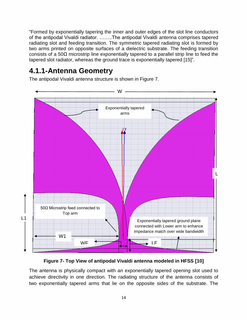
“Formed by exponentially tapering the inner and outer edges of the slot line conductors of the antipodal Vivaldi radiator. ……..The antipodal Vivaldi antenna comprises tapered radiating slot and feeding transition. The symmetric tapered radiating slot is formed by two arms printed on opposite surfaces of a dielectric substrate. The feeding transition consists of a 50Ω microstrip line exponentially tapered to a parallel strip line to feed the tapered slot radiator, whereas the ground trace is exponentially tapered [15]”.
4.1.1-Antenna Geometry The antipodal Vivaldi antenna structure is shown in Figure 7.
Figure 7- Top View of antipodal Vivaldi antenna modeled in HFSS [10]
The antenna is physically compact with an exponentially tapered opening slot used to
achieve directivity in one direction. The radiating structure of the antenna consists of
two exponentially tapered arms that lie on the opposite sides of the substrate. The
Exponentially tapered
arms
50Ω Microstrip feed connected to
Top arm
Exponentially tapered ground plane
connected with Lower arm to enhance
impedance match over wide bandwidth
L
W
WF
L1
W1
LF
15
tapered arm on the top layer of the substrate is fed by a 50Ω microstrip line. The
tapered arm on the bottom layer of substrate is connected with an exponentially tapered
ground plane feed to achieve impedance match over the entire UWB range. The ground
plane feed is most narrow at the micro strip feed and then it spreads out exponentially
on both sides.
According to antenna geometry XY plane ( ) is E-Plane and YZ plane ) is
H-Plane whereas direction of maximum radiation of the antenna is along Y-axis
( , ).
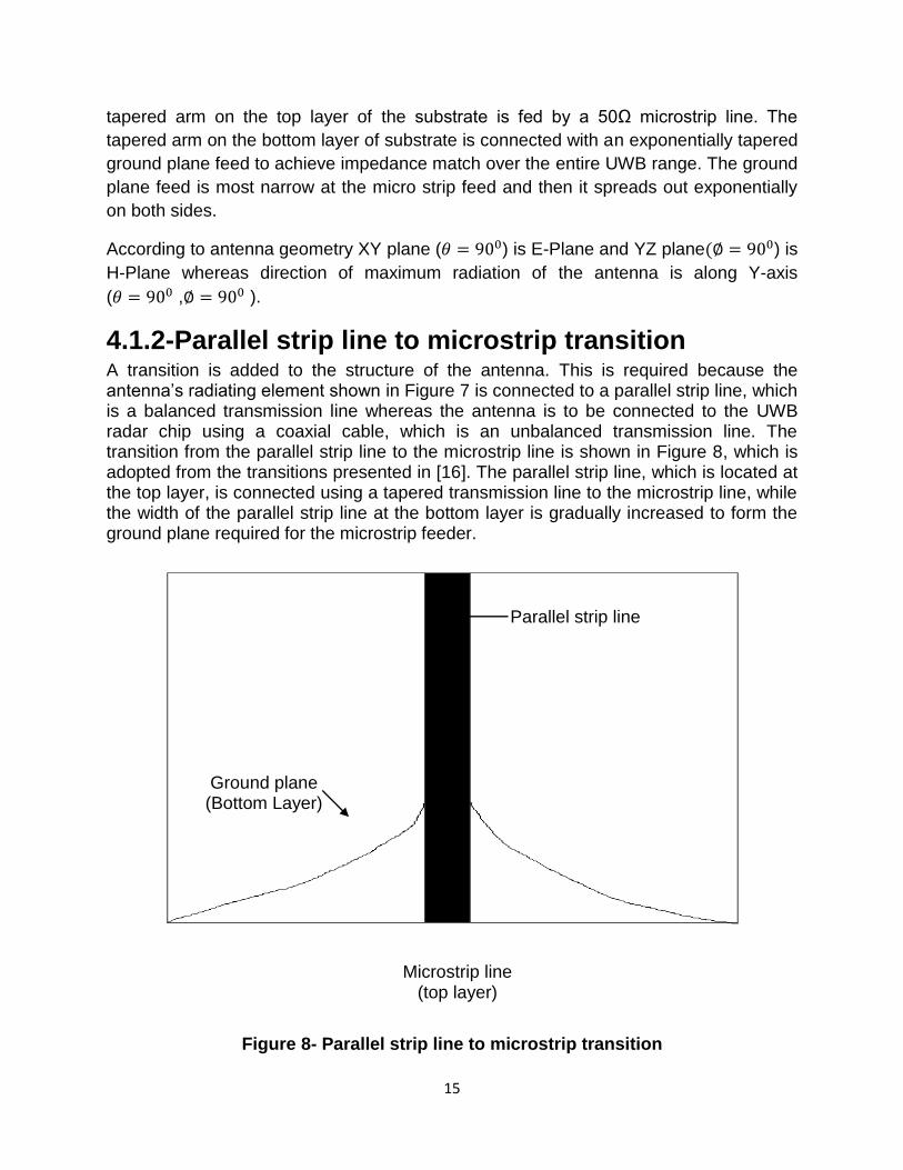
4.1.2-Parallel strip line to microstrip transition A transition is added to the structure of the antenna. This is required because the antenna‟s radiating element shown in Figure 7 is connected to a parallel strip line, which is a balanced transmission line whereas the antenna is to be connected to the UWB radar chip using a coaxial cable, which is an unbalanced transmission line. The transition from the parallel strip line to the microstrip line is shown in Figure 8, which is adopted from the transitions presented in [16]. The parallel strip line, which is located at the top layer, is connected using a tapered transmission line to the microstrip line, while the width of the parallel strip line at the bottom layer is gradually increased to form the ground plane required for the microstrip feeder.
Figure 8- Parallel strip line to microstrip transition
Ground plane (Bottom Layer)
Microstrip line (top layer)
Parallel strip line
16
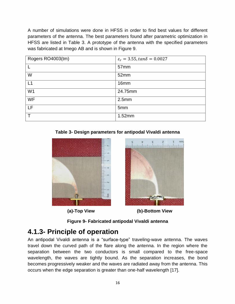
A number of simulations were done in HFSS in order to find best values for different
parameters of the antenna. The best parameters found after parametric optimization in
HFSS are listed in Table 3. A prototype of the antenna with the specified parameters
was fabricated at Imego AB and is shown in Figure 9.
Rogers RO4003(tm)
L 57mm
W 52mm
L1 16mm
W1 24.75mm
WF 2.5mm
LF 5mm
T 1.52mm
Table 3- Design parameters for antipodal Vivaldi antenna
Figure 9- Fabricated antipodal Vivaldi antenna
4.1.3- Principle of operation An antipodal Vivaldi antenna is a “surface-type” traveling-wave antenna. The waves
travel down the curved path of the flare along the antenna. In the region where the
separation between the two conductors is small compared to the free-space
wavelength, the waves are tightly bound. As the separation increases, the bond
becomes progressively weaker and the waves are radiated away from the antenna. This
occurs when the edge separation is greater than one-half wavelength [17].
(a)-Top View (b)-Bottom View
17
4.2- Results and discussion
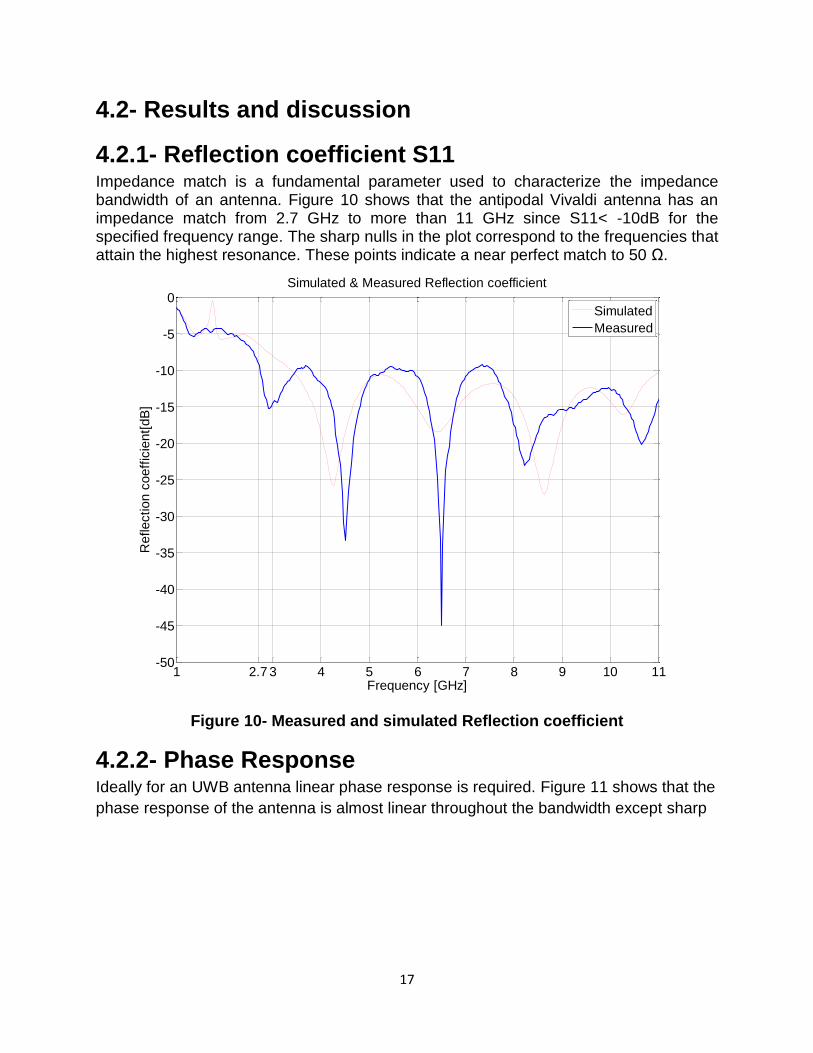
4.2.1- Reflection coefficient S11 Impedance match is a fundamental parameter used to characterize the impedance bandwidth of an antenna. Figure 10 shows that the antipodal Vivaldi antenna has an impedance match from 2.7 GHz to more than 11 GHz since S11< -10dB for the specified frequency range. The sharp nulls in the plot correspond to the frequencies that attain the highest resonance. These points indicate a near perfect match to 50 Ω.
Figure 10- Measured and simulated Reflection coefficient
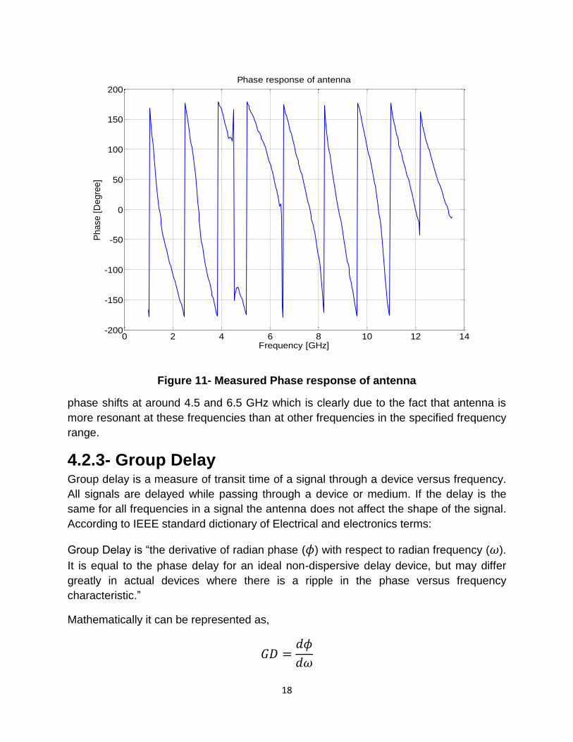
4.2.2- Phase Response Ideally for an UWB antenna linear phase response is required. Figure 11 shows that the
phase response of the antenna is almost linear throughout the bandwidth except sharp
1 2.7 3 4 5 6 7 8 9 10 11-50
-45
-40
-35
-30
-25
-20
-15
-10
-5
0
Frequency [GHz]
Reflection c
oeff
icie
nt[
dB
]
Simulated & Measured Reflection coefficient
Simulated
Measured
18
Figure 11- Measured Phase response of antenna
phase shifts at around 4.5 and 6.5 GHz which is clearly due to the fact that antenna is
more resonant at these frequencies than at other frequencies in the specified frequency
range.
4.2.3- Group Delay Group delay is a measure of transit time of a signal through a device versus frequency.
All signals are delayed while passing through a device or medium. If the delay is the
same for all frequencies in a signal the antenna does not affect the shape of the signal.
According to IEEE standard dictionary of Electrical and electronics terms:
Group Delay is “the derivative of radian phase ( ) with respect to radian frequency ( ).
It is equal to the phase delay for an ideal non-dispersive delay device, but may differ
greatly in actual devices where there is a ripple in the phase versus frequency
characteristic.”
Mathematically it can be represented as,
0 2 4 6 8 10 12 14-200
-150
-100
-50
0
50
100
150
200
Frequency [GHz]
Phase [
Degre
e]
Phase response of antenna
19
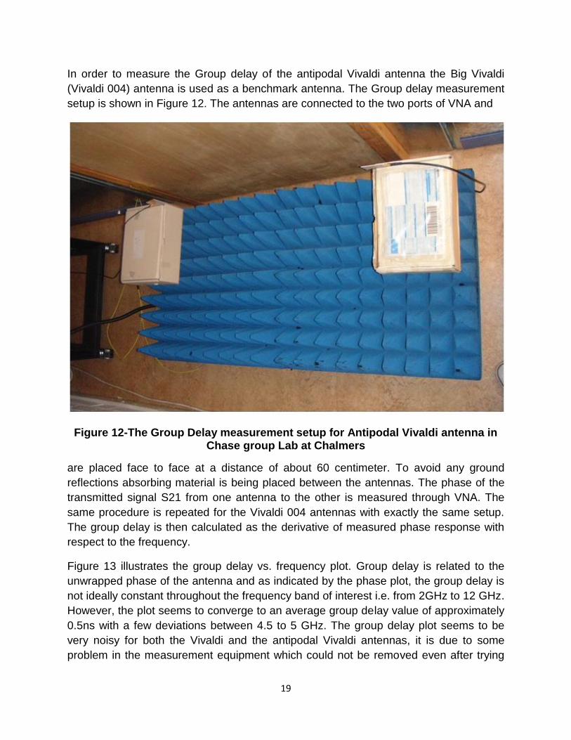
In order to measure the Group delay of the antipodal Vivaldi antenna the Big Vivaldi
(Vivaldi 004) antenna is used as a benchmark antenna. The Group delay measurement
setup is shown in Figure 12. The antennas are connected to the two ports of VNA and
Figure 12-The Group Delay measurement setup for Antipodal Vivaldi antenna in Chase group Lab at Chalmers
are placed face to face at a distance of about 60 centimeter. To avoid any ground
reflections absorbing material is being placed between the antennas. The phase of the
transmitted signal S21 from one antenna to the other is measured through VNA. The
same procedure is repeated for the Vivaldi 004 antennas with exactly the same setup.
The group delay is then calculated as the derivative of measured phase response with
respect to the frequency.
Figure 13 illustrates the group delay vs. frequency plot. Group delay is related to the
unwrapped phase of the antenna and as indicated by the phase plot, the group delay is
not ideally constant throughout the frequency band of interest i.e. from 2GHz to 12 GHz.
However, the plot seems to converge to an average group delay value of approximately
0.5ns with a few deviations between 4.5 to 5 GHz. The group delay plot seems to be
very noisy for both the Vivaldi and the antipodal Vivaldi antennas, it is due to some
problem in the measurement equipment which could not be removed even after trying
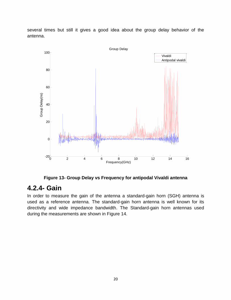
20
several times but still it gives a good idea about the group delay behavior of the
antenna.
Figure 13- Group Delay vs Frequency for antipodal Vivaldi antenna
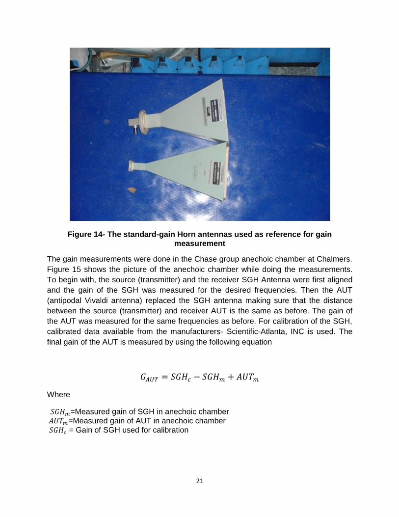
4.2.4- Gain In order to measure the gain of the antenna a standard-gain horn (SGH) antenna is
used as a reference antenna. The standard-gain horn antenna is well known for its
directivity and wide impedance bandwidth. The Standard-gain horn antennas used
during the measurements are shown in Figure 14.
0 2 4 6 8 10 12 14 16-20
0
20
40
60
80
100
Frequency(GHz)
Gro
up D
ela
y(n
s)
Group Delay
Vivaldi
Antipodal vivaldi
21
Figure 14- The standard-gain Horn antennas used as reference for gain measurement
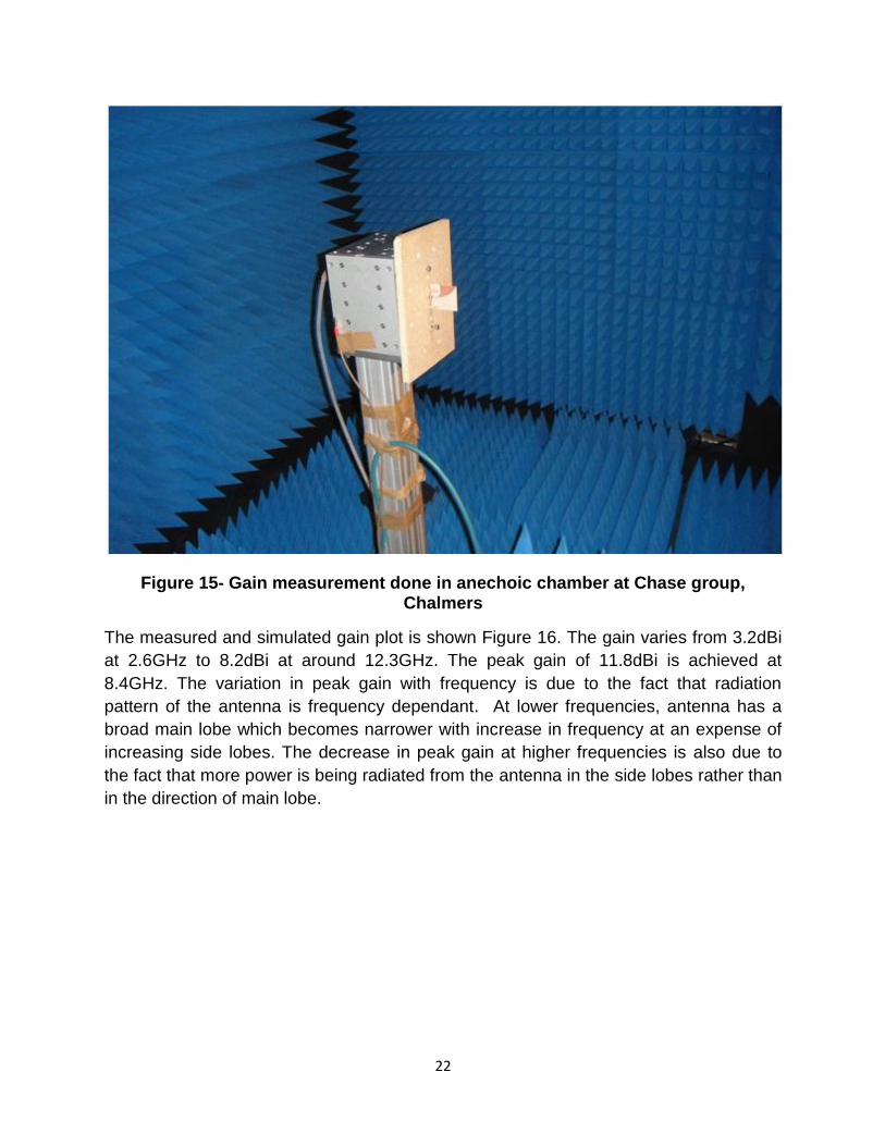
The gain measurements were done in the Chase group anechoic chamber at Chalmers.
Figure 15 shows the picture of the anechoic chamber while doing the measurements.
To begin with, the source (transmitter) and the receiver SGH Antenna were first aligned
and the gain of the SGH was measured for the desired frequencies. Then the AUT
(antipodal Vivaldi antenna) replaced the SGH antenna making sure that the distance
between the source (transmitter) and receiver AUT is the same as before. The gain of
the AUT was measured for the same frequencies as before. For calibration of the SGH,
calibrated data available from the manufacturers- Scientific-Atlanta, INC is used. The
final gain of the AUT is measured by using the following equation
Where
=Measured gain of SGH in anechoic chamber =Measured gain of AUT in anechoic chamber = Gain of SGH used for calibration
22
Figure 15- Gain measurement done in anechoic chamber at Chase group, Chalmers
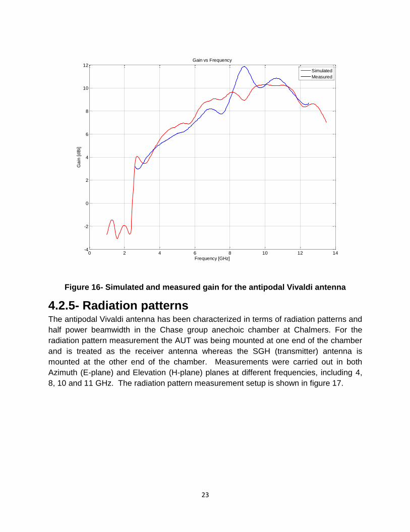
The measured and simulated gain plot is shown Figure 16. The gain varies from 3.2dBi
at 2.6GHz to 8.2dBi at around 12.3GHz. The peak gain of 11.8dBi is achieved at
8.4GHz. The variation in peak gain with frequency is due to the fact that radiation
pattern of the antenna is frequency dependant. At lower frequencies, antenna has a
broad main lobe which becomes narrower with increase in frequency at an expense of
increasing side lobes. The decrease in peak gain at higher frequencies is also due to
the fact that more power is being radiated from the antenna in the side lobes rather than
in the direction of main lobe.
23
Figure 16- Simulated and measured gain for the antipodal Vivaldi antenna
4.2.5- Radiation patterns The antipodal Vivaldi antenna has been characterized in terms of radiation patterns and
half power beamwidth in the Chase group anechoic chamber at Chalmers. For the
radiation pattern measurement the AUT was being mounted at one end of the chamber
and is treated as the receiver antenna whereas the SGH (transmitter) antenna is
mounted at the other end of the chamber. Measurements were carried out in both
Azimuth (E-plane) and Elevation (H-plane) planes at different frequencies, including 4,
8, 10 and 11 GHz. The radiation pattern measurement setup is shown in figure 17.
0 2 4 6 8 10 12 14-4
-2
0
2
4
6
8
10
12
Frequency [GHz]
Ga
in [d
Bi]
Gain vs Frequency
Simulated
Measured
24
At 4 GHz, azimuth plane pattern exhibits HPBW of around . The first side lobe
appears to be 11dB below the main lobe. The elevation plane pattern reveals a broader
beam with a HPBW of around and first back lobe is 14dB below the main lobe. The
normalized co and cross polar radiation patterns in both planes at frequency of 4 GHz
are shown in Figure 18.
Transmitter Antenna AUT
Elevation Plane
Azimuth Plane
Figure 17- Radiation Pattern measurement setup
25
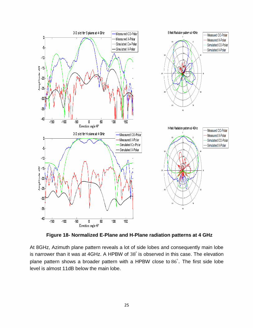
At 8GHz, Azimuth plane pattern reveals a lot of side lobes and consequently main lobe
is narrower than it was at 4GHz. A HPBW of is observed in this case. The elevation
plane pattern shows a broader pattern with a HPBW close to . The first side lobe
level is almost 11dB below the main lobe.
Figure 18- Normalized E-Plane and H-Plane radiation patterns at 4 GHz
25
As frequency is increasing the main lobe is becoming more and more directive as can
be seen in the azimuth plane pattern at 10 GHz shown in Figure 20. The side lobes
have increased in number with a corresponding decrease in their magnitude levels. The
cross polarization level is below -20dB in the direction of maximum radiation. A HPBW
of around is observed in this case. The gain at 10 GHz is around 10.2dBi. The
elevation plane pattern shows similar characteristics but with a HPBW of around .
Figure 18- Normalized Azimuth and Elevation Plane radiation patterns at 8 GHz
Figure 19- Normalized E-Plane and H-Plane radiation patterns at 8 GHz
26
At 11GHz, azimuth and elevation plane patterns still show directive properties but the
main lobe is much wider than before. HPBW in azimuth plane is around whereas in
elevation plane it is around Cross polarization is overlapping the co polarization
level on the side lobes.
Figure 20- Normalized E-Plane and H-Plane radiation patterns at 10 GHz
27
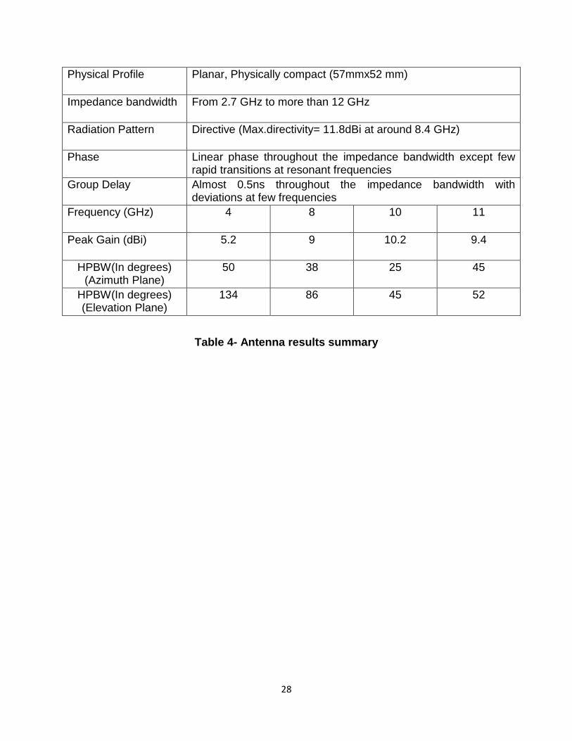
4.2.6- Summary The antenna characteristics with measured results are summarized in table 4. The
results show that due to the planar profile, physically compact size, wide impedance
bandwidth and directive performance over a wide bandwidth the antipodal Vivaldi
antenna is a good candidate for use with the Novelda UWB radar chip and other UWB
integrated circuits and portable electronics.
Figure 21- Normalized E-Plane and H-Plane radiation patterns at 11 GHz
28
Physical Profile Planar, Physically compact (57mmx52 mm)
Impedance bandwidth From 2.7 GHz to more than 12 GHz
Radiation Pattern Directive (Max.directivity= 11.8dBi at around 8.4 GHz)
Phase Linear phase throughout the impedance bandwidth except few rapid transitions at resonant frequencies
Group Delay Almost 0.5ns throughout the impedance bandwidth with deviations at few frequencies
Frequency (GHz) 4 8 10 11
Peak Gain (dBi) 5.2 9 10.2 9.4
HPBW(In degrees) (Azimuth Plane)
50 38 25 45
HPBW(In degrees) (Elevation Plane)
134 86 45 52
Table 4- Antenna results summary
29
Chapter 5
Conclusions and future work
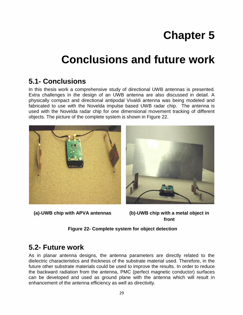
5.1- Conclusions In this thesis work a comprehensive study of directional UWB antennas is presented. Extra challenges in the design of an UWB antenna are also discussed in detail. A physically compact and directional antipodal Vivaldi antenna was being modeled and fabricated to use with the Novelda impulse based UWB radar chip. The antenna is used with the Novelda radar chip for one dimensional movement tracking of different objects. The picture of the complete system is shown in Figure 22.
5.2- Future work As in planar antenna designs, the antenna parameters are directly related to the dielectric characteristics and thickness of the substrate material used. Therefore, in the future other substrate materials could be used to improve the results. In order to reduce the backward radiation from the antenna, PMC (perfect magnetic conductor) surfaces can be developed and used as ground plane with the antenna which will result in enhancement of the antenna efficiency as well as directivity.
(a)-UWB chip with APVA antennas (b)-UWB chip with a metal object in
front
Figure 22- Complete system for object detection
30
The Novelda impulse based UWB radar chip promise to be at the heart of many applications in the field of medical diagnosis and health monitoring. New planar, directional UWB antennas for these kinds of applications need to be developed. Heart beat and human breathing detection is also possible with impulse based radar chips. New compact directive antennas operable over the lower frequency band of the UWB range are needed to be developed so that these antennas can be placed on the human chest and penetrate through it in order to capture small changes in signal level caused by the continuous motion of the heart.
31
References [1] Federal Communications Commission. Uwb emission limit for indoor systems, feb 2002. http://www.fcc.gov/Bureaus/Engineering_Technology/News_Releases/ 2002/nret0203.ppt [2] John S. Belrose. The Sounds of a Spark Transmitter: Telegraphy and Telephony. Adventures in CyberSound. [3] Dr. Robert J. Fontana. A Brief History of UWB Communications. Multispectrum Solutions, Inc. [4] V. H. Rumsey, “Frequency Independent Antennas,” 1957 IRE National Convention Record, pt. 1, pp. 114-118. [5] J.D. Dyson, “The Unidirectional Equiangular Spiral Antenna,” IRE Trans. Antennas Propagat., Vol. AP-7, pp. 329-334, October 1959. [6] Ross, G.F., 1968, A time domain criterion for the design of wideband radiating elements, IEEE Trans. Antennas Propagat., Vol. 16, No. 3, p. 355. [7] Dr. Tarance W. Barrett. History of Ultra Wideband (UWB) Radar & Communications: Pioneers and Innovators. [8] Oppermann, Hamalainen, and Linatti, UWB Theory and Applications, Wiley,2004. [9] Introduction to UWB: Impulse Radio for Radar and Wireless Communications by Dr. Jeffrey Reed, Dr. R. Michael Buehrer, David McKinstry. [10] Ansoft.com. [11] www.Novelda.no. [12] C. A. Balanis, Antenna Theory Analysis and Design, 3rd edition, Wiley-Interscience, 2005. [13] Merrill Skolnik, Radar Handbook, 2nd edition, McGraw-Hill, 1990. [14] Gazit, “Improved design of a Vivaldi antenna,” IEEE Proc. H, 1988, pp 89-92.
[15] B. Allen et al., Ultra-wideband Antennas and Propagation for Communications, Radar and Imaging, Wiley, 2007.
32
[16] S.-G. Kim and K. Chang, “Ultrawide-band transitions and new microwave components using double-sided parallel-strip lines,” IEEE Transactions onMicrowave Theory and Techniques, vol. 52, no. 9, part 1, pp. 2148–2152, 2004. [17] Gibson, P.J., “The Vivaldi aerial,” Proc. 9th European Microwave Conference, 1979, pp. 103-105.
Recommended