Freescale SemiconductorApplication Note
AN2759Rev. 0.2, 9/2004
®
Implementing an Ethernet Interface with the MC9S12NE64By: Bill Lucas and Steven Torres
Systems Engineering Austin, Texas
Introduction
This application note provides recommendations for implementing an Ethernet interface with the MC9S12NE64 microcontroller unit (MCU). The discussion covers many topics including:
• Overview of the MC9S12NE64 including available packages
• Components required to add Ethernet functionality to the MC9S12NE64
• MC9S12NE64 schematics showing the minimum system design
• Circuit connections between the MC9S12NE64 and a high-speed LAN magnetics isolation module and RJ45 connector
• General printed circuit board (PCB) layout recommendations for 10 and 100 Mbps Ethernet design
• High-speed LAN magnetics isolation module requirements
• Crystal placement and circuitry recommendations
• MC9S12NE64 Ethernet design examples in both 112-pin and 80-pin packages
© Freescale Semiconductor, Inc., 2004. All rights reserved.
This product incorporates SuperFlash technology licensed from SST.
MC9S12NE64 Single-Chip Ethernet Solution
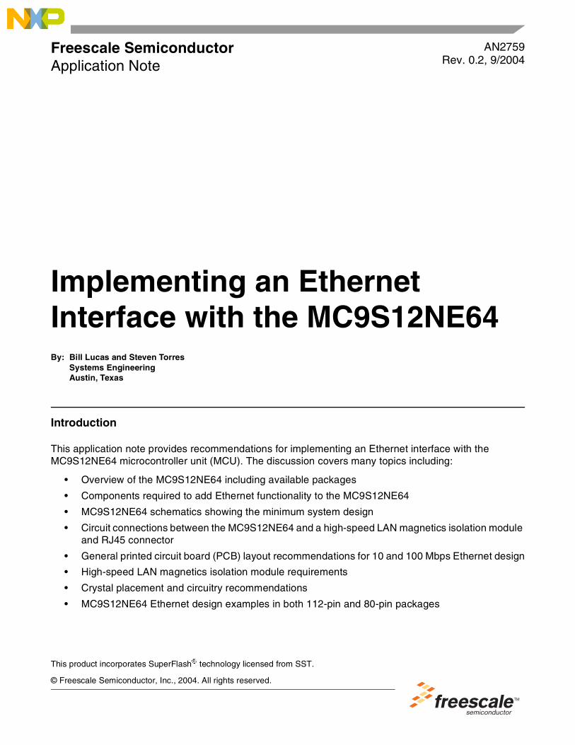
Figure 1 shows a preview of the design examples:
Figure 1. Design Examples
MC9S12NE64 Single-Chip Ethernet Solution
This section introduces the MC9S12NE64 and provides an overview of the MC9S12NE64 integrated Ethernet controller and MC9S12NE64 system design.
MC9S12NE64 Overview
The MC9S12NE64 is a 16-bit MCU based on Freescale Semiconductor’s HCS12 CPU platform. It includes 8K bytes of RAM and 64K bytes of FLASH memory. In the 80-pin package, the MC9S12NE64 has other standard on-chip peripherals including two asynchronous serial communications interface modules (SCIs), one synchronous serial peripheral interface (SPI), an inter-integrated circuit bus (IIC), a 4-channel/16-bit timer module (TIM), an 8-channel/10-bit analog-to-digital converter (ADC), and up to 18 pins available as keypad wake-up inputs (KWUs) or general-purpose I/O pins. In addition, an expanded bus that can be operated at 16 MHz1 is available on the 112-pin package.
The MC9S12NE64 introduces a new peripheral for the HCS12 CPU platform, an integrated Ethernet controller. The MC9S12NE64 integrates an Ethernet controller that includes a media access controller (MAC) and a physical transceiver (PHY) in one die with the CPU, memory, and other HCS12 standard on-chip peripherals. The MC9S12NE64 integrated Ethernet controller is compatible with IEEE 802.3 and 802.3u specifications for 10-Mbps or 100-Mbps operation, respectively.
1. At a 16-MHz internal bus speed, the MC9S12NE64 integrated Ethernet controller is limited to 10-Mbps operation. A 25-MHz internal bus speed is required for 100-Mbps operation.
Implementing an Ethernet Interface with the MC9S12NE64, Rev. 0.2
2 Freescale Semiconductor
MC9S12NE64 Single-Chip Ethernet Solution
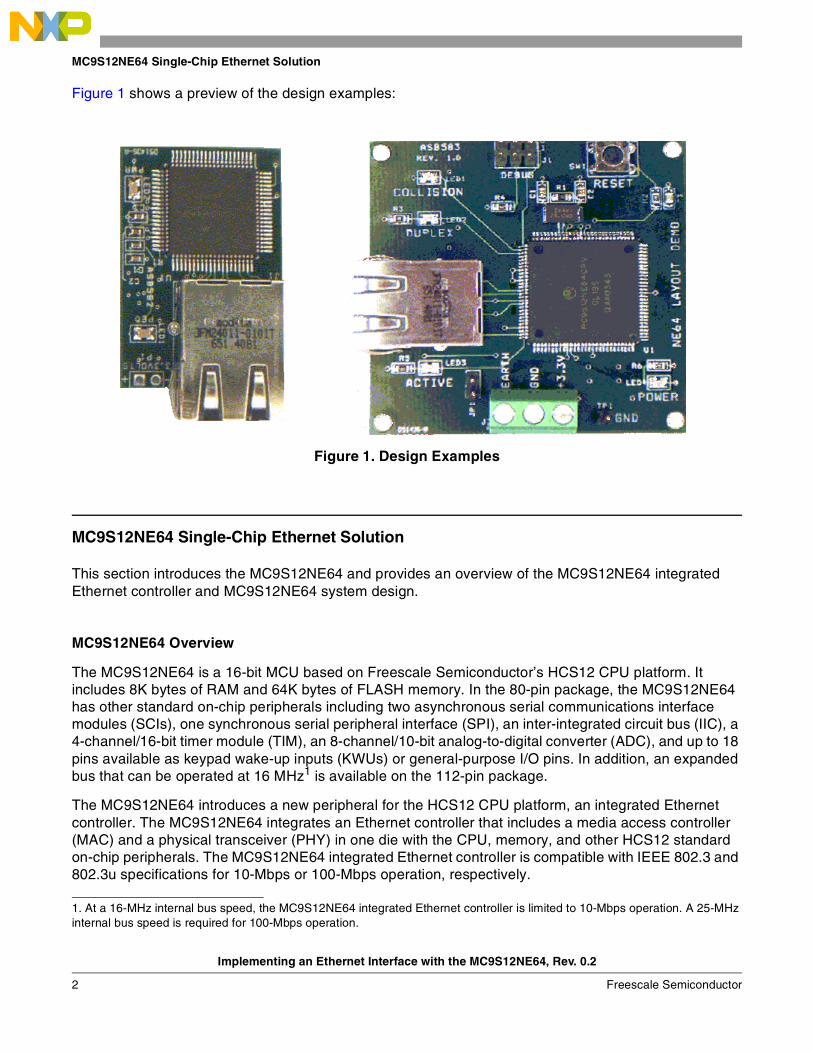
The MC9S12NE64 can be targeted at low-throughput connectivity applications that require operation from a nominal 3.3-V power supply. With an on-chip bandgap-based voltage regulator (VREG), the internal digital supply voltage of 2.5 V (VDD) will be generated internally. Figure 2 shows a block diagram of the MC9S12NE64. More information on the MC9S12NE64 is available from the Freescale Semiconductor website: http://freescale.com.
Figure 2. Block Diagram of the MC9S12NE64
MC9S12NE64 Packages
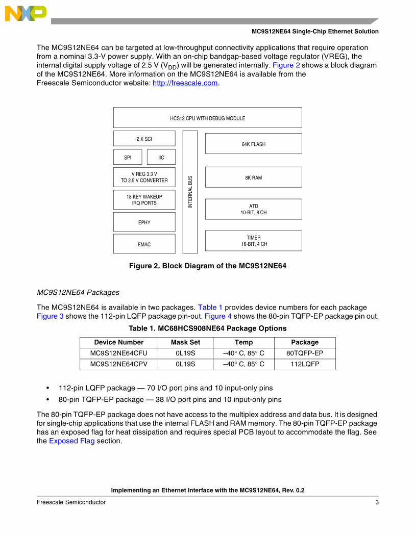
The MC9S12NE64 is available in two packages. Table 1 provides device numbers for each package Figure 3 shows the 112-pin LQFP package pin-out. Figure 4 shows the 80-pin TQFP-EP package pin out.
• 112-pin LQFP package — 70 I/O port pins and 10 input-only pins
• 80-pin TQFP-EP package — 38 I/O port pins and 10 input-only pins
The 80-pin TQFP-EP package does not have access to the multiplex address and data bus. It is designed for single-chip applications that use the internal FLASH and RAM memory. The 80-pin TQFP-EP package has an exposed flag for heat dissipation and requires special PCB layout to accommodate the flag. See the Exposed Flag section.
Table 1. MC68HCS908NE64 Package Options
Device Number Mask Set Temp Package
MC9S12NE64CFU 0L19S –40° C, 85° C 80TQFP-EP
MC9S12NE64CPV 0L19S –40° C, 85° C 112LQFP
HCS12 CPU WITH DEBUG MODULE
2 X SCI
SPI IIC
V REG 3.3 VTO 2.5 V CONVERTER
18 KEY WAKEUPIRQ PORTS
EPHY
EMAC
64K FLASH
8K RAM
ATD10-BIT, 8 CH
INTE
RN
AL B
US
TIMER 16-BIT, 4 CH
Implementing an Ethernet Interface with the MC9S12NE64, Rev. 0.2
Freescale Semiconductor 3
MC9S12NE64 Single-Chip Ethernet Solution
Figure 3. Pinout of MC9S12NE64 in 112-Pin LQFP Package
PL0/ACTLEDPL1/LNKLEDVDDRPL2/SPDLEDPA7/ADDR15/DATA15PA6/ADDR14/DATA14PA5/ADDR13/DATA13PA4/ADDR12/DATA12PHY_VSSRXPHY_VDDRXPHY_RXN PHY_RXPPHY_VSSTXPHY_TXNPHY_TXPPHY_VDDTXPHY_VDDAPHY_VSSAPHY_RBIASVDD2VSS2PA3/ADDR11/DATA11PA2/ADDR10/DATA10PA1/ADDR9/DATA9PA0/ADDR8/DATA8PL3/DUPLEDPL4/COLLEDBKGD/MODC
PJ6
/KW
J6/I
IC_S
DA
PJ7
/KW
J7/I
IC_S
CL
PT
4/T
IM_I
OC
4P
T5/
TIM
_IO
C5
PT
6/T
IM_I
OC
6P
T7/
TIM
_IO
C7
PK
7/E
CS
/RO
MC
TL
PK
6/X
CS
PK
5/X
AD
DR
19P
K4/
XA
DD
R18
VD
D1
VS
S1
PK
3/X
AD
DR
17P
K2/
XA
DD
R16
PK
1/X
AD
DR
15P
K0/
XA
DD
R14
VS
SA
VR
LV
RH
VD
DA
PAD
7/A
N7
PAD
6/A
N6
PAD
5/A
N5
PAD
4/A
N4
PAD
3/A
N3
PAD
2/A
N2
PAD
1/A
N1
PAD
0/A
N0
MII_TXER/KWH6/PH6MII_TXEN/KWH5/PH5
MII_TXCLK/KWH4/PH4MII_TXD3/KWH3/PH3MII_TXD2/KWH2/PH2MII_TXD1/KWH1/PH1MII_TXD0/KWH0/PH0
MII_MDC/KWJ0/PJ0MII_MDIO/KWJ1/PJ1ADDR0/DATA0/PB0ADDR1/DATA1/PB1ADDR2/DATA2/PB2ADDR3/DATA3/PB3
VDDX1VSSX1
ADDR4/DATA4/PB4ADDR5/DATA5/PB5ADDR6/DATA6/PB6ADDR7/DATA7/PB7MII_CRS/KWJ2/PJ2MII_COL/KWJ3/PJ3
MII_RXD0/KWG0/PG0MII_RXD1/KWG1/PG1MII_RXD2/KWG2/PG2MII_RXD3/KWG3/PG3
MII_RXCLK/KWG4/PG4MII_RXDV/KWG5/PG5MII_RXER/KWG6/PG6
KW
G7/
PG
7S
CI0
_RX
D/P
S0
SC
I0_T
XD
/PS
1S
CI1
_RX
D/P
S2
SC
I1_T
XD
/PS
3S
PI_
MIS
O/P
S4
SP
I_M
OS
I/P
S5
SP
I_S
CK
/PS
6S
PI_
SS
/PS
7N
OA
CC
/PE
7M
OD
B/IP
IPE
1/P
E6
MO
DA
/IPIP
E0/
PE
5E
CLK
/PE
4V
SS
X2
VD
DX
2R
ES
ET
VD
DP
LLX
FC
VS
SP
LLE
XTA
LX
TAL
TE
ST
PL
6P
L5
LS
TR
B/T
AG
LO
/PE
3R
/W/P
E2
IRQ
/ PE
1X
IRQ
/PE
0
Signals shown in Bold are not available on the 80-pin package.
MC9S12NE64-Family112LQFP
112
111
110
109
108
107
106
105
104
103
102
101
100 99 98 97 96 95 94 93 92 91 90 89 88 87 86 851
2345678910111213141516171819202122232425262728
29 30 31 32 33 34 35 36 37 38 39 40 41 42 43 44 45 46 47 48 49 50 51 52 53 54 55 56
84838281807978777675747372717069686766656463626160595857
Implementing an Ethernet Interface with the MC9S12NE64, Rev. 0.2
4 Freescale Semiconductor
MC9S12NE64 Single-Chip Ethernet Solution
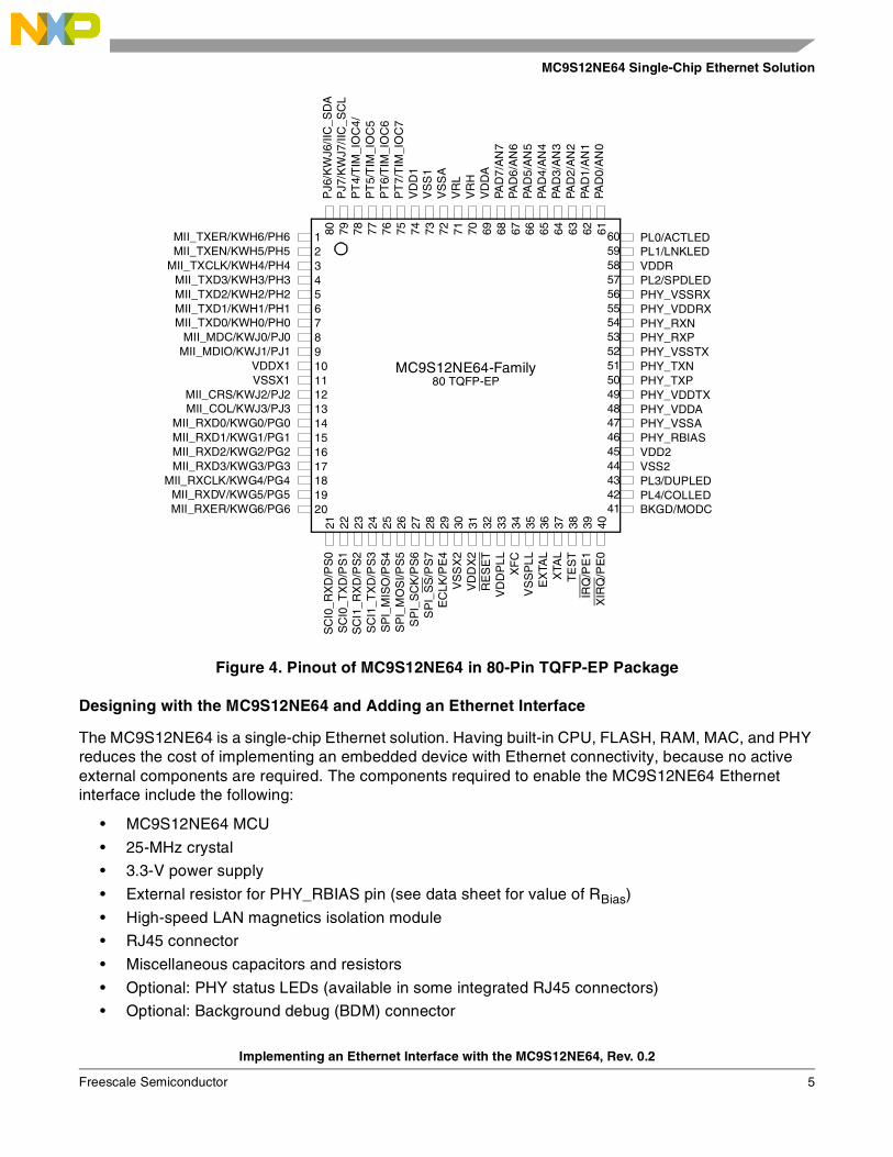
Figure 4. Pinout of MC9S12NE64 in 80-Pin TQFP-EP Package
Designing with the MC9S12NE64 and Adding an Ethernet Interface
The MC9S12NE64 is a single-chip Ethernet solution. Having built-in CPU, FLASH, RAM, MAC, and PHY reduces the cost of implementing an embedded device with Ethernet connectivity, because no active external components are required. The components required to enable the MC9S12NE64 Ethernet interface include the following:
• MC9S12NE64 MCU
• 25-MHz crystal
• 3.3-V power supply
• External resistor for PHY_RBIAS pin (see data sheet for value of RBias)
• High-speed LAN magnetics isolation module
• RJ45 connector
• Miscellaneous capacitors and resistors
• Optional: PHY status LEDs (available in some integrated RJ45 connectors)
• Optional: Background debug (BDM) connector
1234567891011121314151617181920
80 79 78 77 76 75 74 73 72 71 70 69 68 67 66 65 64 63 62 61
21 22 23 24 25 26 27 28 29 30 31 32 33 34 35 36 37 38 39 40
MC9S12NE64-Family80 TQFP-EP
PL0/ACTLEDPL1/LNKLEDVDDRPL2/SPDLEDPHY_VSSRXPHY_VDDRXPHY_RXN PHY_RXPPHY_VSSTXPHY_TXNPHY_TXPPHY_VDDTXPHY_VDDAPHY_VSSAPHY_RBIASVDD2VSS2PL3/DUPLEDPL4/COLLEDBKGD/MODC
PJ6
/KW
J6/II
C_S
DA
PJ7
/KW
J7/II
C_S
CL
PT
4/T
IM_I
OC
4/P
T5/
TIM
_IO
C5
PT
6/T
IM_I
OC
6P
T7/
TIM
_IO
C7
VD
D1
VS
S1
VS
SA
VR
LV
RH
VD
DA
PAD
7/A
N7
PAD
6/A
N6
PAD
5/A
N5
PAD
4/A
N4
PAD
3/A
N3
PAD
2/A
N2
PAD
1/A
N1
PAD
0/A
N0
MII_TXER/KWH6/PH6MII_TXEN/KWH5/PH5
MII_TXCLK/KWH4/PH4MII_TXD3/KWH3/PH3MII_TXD2/KWH2/PH2MII_TXD1/KWH1/PH1MII_TXD0/KWH0/PH0
MII_MDC/KWJ0/PJ0MII_MDIO/KWJ1/PJ1
VDDX1VSSX1
MII_CRS/KWJ2/PJ2MII_COL/KWJ3/PJ3
MII_RXD0/KWG0/PG0MII_RXD1/KWG1/PG1MII_RXD2/KWG2/PG2MII_RXD3/KWG3/PG3
MII_RXCLK/KWG4/PG4MII_RXDV/KWG5/PG5MII_RXER/KWG6/PG6
SC
I0_R
XD
/PS
0S
CI0
_TX
D/P
S1
SC
I1_R
XD
/PS
2S
CI1
_TX
D/P
S3
SP
I_M
ISO
/PS
4S
PI_
MO
SI/P
S5
SP
I_S
CK
/PS
6S
PI_
SS
/PS
7E
CLK
/PE
4V
SS
X2
VD
DX
2R
ES
ET
VD
DP
LLX
FC
VS
SP
LLE
XTA
LX
TAL
TE
ST
IRQ
/ PE
1X
IRQ
/PE
0
6059585756555453525150494847464544434241
Implementing an Ethernet Interface with the MC9S12NE64, Rev. 0.2
Freescale Semiconductor 5
MC9S12NE64 Single-Chip Ethernet Solution
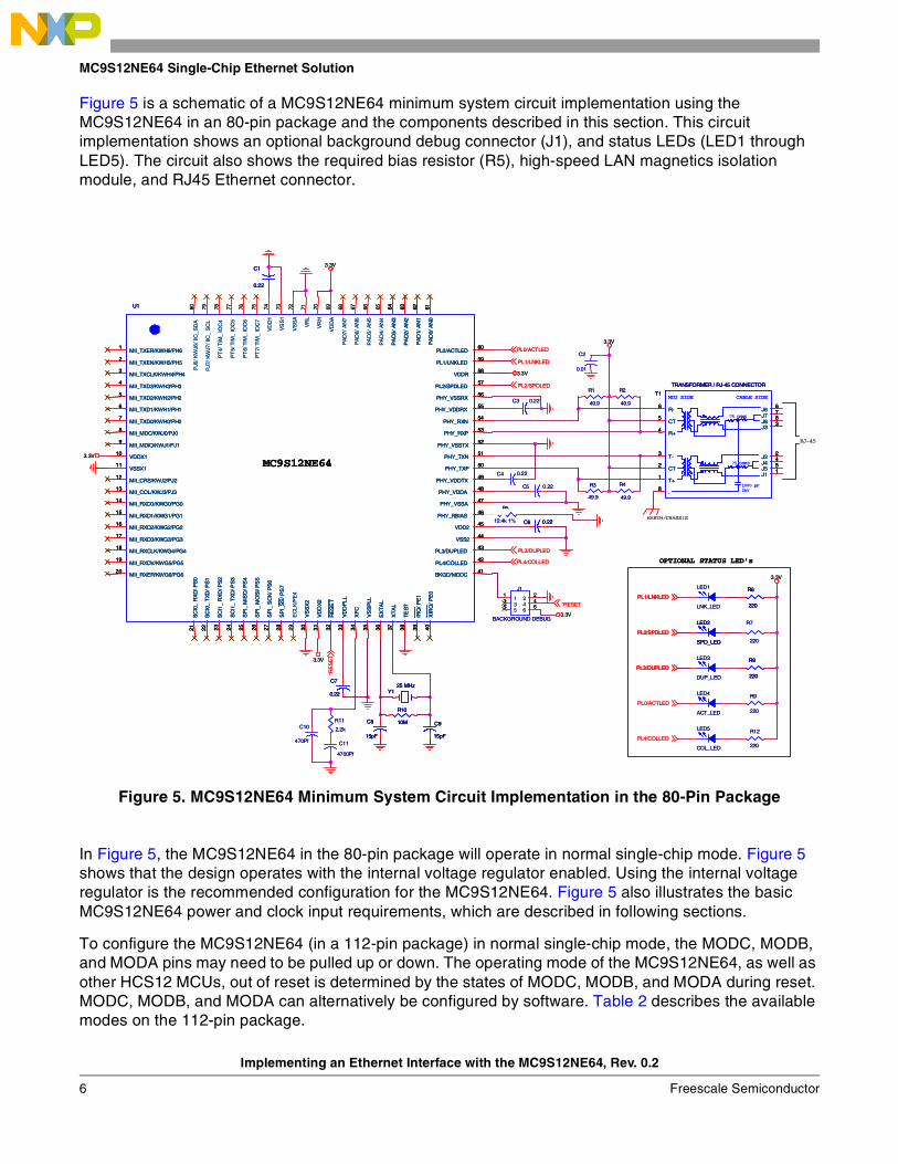
Figure 5 is a schematic of a MC9S12NE64 minimum system circuit implementation using the MC9S12NE64 in an 80-pin package and the components described in this section. This circuit implementation shows an optional background debug connector (J1), and status LEDs (LED1 through LED5). The circuit also shows the required bias resistor (R5), high-speed LAN magnetics isolation module, and RJ45 Ethernet connector.
Figure 5. MC9S12NE64 Minimum System Circuit Implementation in the 80-Pin Package
In Figure 5, the MC9S12NE64 in the 80-pin package will operate in normal single-chip mode. Figure 5 shows that the design operates with the internal voltage regulator enabled. Using the internal voltage regulator is the recommended configuration for the MC9S12NE64. Figure 5 also illustrates the basic MC9S12NE64 power and clock input requirements, which are described in following sections.
To configure the MC9S12NE64 (in a 112-pin package) in normal single-chip mode, the MODC, MODB, and MODA pins may need to be pulled up or down. The operating mode of the MC9S12NE64, as well as other HCS12 MCUs, out of reset is determined by the states of MODC, MODB, and MODA during reset. MODC, MODB, and MODA can alternatively be configured by software. Table 2 describes the available modes on the 112-pin package.
75 OHMS
75 OHMS
1000 pF2kV
CABLE SIDEMCU SIDET1
TRANSFORMER / RJ-45 CONNECTOR
T+1
CT2
T-3
R+4
CT5
R-6
J77
J33
J22
J55J44
J11
.8
J88
J66
R11
2.2kC10
470Pf C11
4700Pf
R3
49.9
R1
49.9
R2
49.9
R4
49.9
3.3V
C2
0.01
MC9S12NE64
EARTH/CHASSIS
3.3V
J1
BACKGROUND DEBUG
11
33
55
22
44
66 *RESET
RJ-45
R5
12.4k 1%
PL1/LNKLED
PL3/DUPLED
PL2/SPDLED
3.3V
3.3V
3.3V
3.3V
*RE
SE
T3.3V
C3 0.22
C4 0.22
C5 0.22
PL0/ACTLED
PL4/COLLED
LED3
DUP_LED
R7
220
LED1
LNK_LED
R6
220
R8
220
LED2
SPD_LED
Y125 MHz
C8
15pF
C9
15pF
C7
0.22
R10
10M
PL3/DUPLED
PL1/LNKLED
PL2/SPDLED
C6 0.22
C1
0.22
U1
MII_TXER/KWH6/PH61
MII_TXEN/KWH5/PH52
MII_TXCLK/KWH4/PH43
MII_TXD3/KWH3/PH34
MII_TXD2/KWH2/PH25
MII_TXD1/KWH1/PH16
MII_TXD0/KWH0/PH07
MII_MDC/KWJ0/PJ08
MII_MDIO/KWJ1/PJ19
VDDX110
VSSX111
MII_CRS/KWJ2/PJ212
MII_COL/KWJ3/PJ313
MII_RXD0/KWG0/PG014
MII_RXD1/KWG1/PG115
MII_RXD2/KWG2/PG216
MII_RXD3/KWG3/PG317
MII_RXCLK/KWG4/PG418
MII_RXDV/KWG5/PG519
MII_RXER/KWG6/PG620
SC
I0_
RX
D/
PS
02
1
SC
I0_
TX
D/
PS
12
2
SC
I1_
RX
D/ P
S2
23
SC
I1_
TX
D/ P
S3
24
SP
I_ M
ISO
/ PS
42
5
SP
I_ M
OS
I/ P
S5
26
SP
I_ S
CK
/ P
S6
27
SP
I_S
S/ P
S7
28
VS
SX
23
0
VD
DX
23
1
RE
SE
T3
2
VD
DP
LL
33
XF
C3
4
VS
SP
LL3
5
EX
TA
L3
6
XT
AL
37
TE
ST
38
IRQ
/ P
E1
39
XIR
Q/
PE
04
0
BKGD/MODC41
PL4/COLLED42
PL3/DUPLED43
VSS244
VDD245
PHY_RBIAS46
PHY_VSSA47
PHY_VDDA48
PHY_VDDTX49
PHY_TXP50
PHY_TXN51
PHY_VSSTX52
PHY_RXP53
PHY_RXN54
PHY_VDDRX55
PHY_VSSRX56
PL2/SPDLED57
VDDR58
PL1/LNKLED59
PL0/ACTLED60
PA
D0/
AN
061
PA
D1/
AN
162
PA
D2
/ A
N2
63
PA
D3
/ A
N3
64
PA
D4
/ A
N4
65
PA
D5
/ A
N5
66
PA
D6/
AN
667
PA
D7/
AN
768
VD
DA
69
VR
H70
VR
L71
VS
SA
72
VS
S1
73
VD
D1
74
PT
7/ T
IM_
IOC
775
PT
6/ T
IM_
IOC
676
PT
5/ T
IM_
IOC
577
PT
4/ T
IM_
IOC
478
PJ7
/ K
WJ7
/ IIC
_ S
CL
79
PJ6
/ KW
J6/ I
IC_
SD
A80
EC
LK
/PE
42
9
LED5
COL_LED
R9
220
R12
220
LED4
ACT_LED
PL4/COLLED
PL0/ACTLED
OPTIONAL STATUS LED's
75 OHMS
75 OHMS
1000 pF2kV
CABLE SIDEMCU SIDET1
TRANSFORMER / RJ-45 CONNECTOR
T+1
CT2
T-3
R+4
CT5
R-6
J77
J33
J22
J55J44
J11
.8
J88
J66
75 OHMS
75 OHMS
1000 pF2kV
CABLE SIDEMCU SIDET1
TRANSFORMER / RJ-45 CONNECTOR
T+1
CT2
T-3
R+4
CT5
R-6
J77
J33
J22
J55J44
J11
.8
J88
J66
R11
2.2kC10
470Pf C11
4700Pf
R3
49.9
R1
49.9
R2
49.9
R4
49.9
3.3V
C2
0.01
MC9S12NE64
EARTH/CHASSIS
3.3V
J1
BACKGROUND DEBUG
11
33
55
22
44
66 *RESET
RJ-45
R5
12.4k 1%
PL1/LNKLED
PL3/DUPLED
PL2/SPDLED
3.3V
3.3V
3.3V
3.3V
*RE
SE
T3.3V
C3 0.22
C4 0.22
C5 0.22
PL0/ACTLED
PL4/COLLED
LED3
DUP_LED
R7
220
LED1
LNK_LED
R6
220
R8
220
LED2
SPD_LED
Y125 MHz
C8
15pF
C9
15pF
C7
0.22
R10
10M
PL3/DUPLED
PL1/LNKLED
PL2/SPDLED
C6 0.22
C1
0.22
U1
MII_TXER/KWH6/PH61
MII_TXEN/KWH5/PH52
MII_TXCLK/KWH4/PH43
MII_TXD3/KWH3/PH34
MII_TXD2/KWH2/PH25
MII_TXD1/KWH1/PH16
MII_TXD0/KWH0/PH07
MII_MDC/KWJ0/PJ08
MII_MDIO/KWJ1/PJ19
VDDX110
VSSX111
MII_CRS/KWJ2/PJ212
MII_COL/KWJ3/PJ313
MII_RXD0/KWG0/PG014
MII_RXD1/KWG1/PG115
MII_RXD2/KWG2/PG216
MII_RXD3/KWG3/PG317
MII_RXCLK/KWG4/PG418
MII_RXDV/KWG5/PG519
MII_RXER/KWG6/PG620
SC
I0_
RX
D/
PS
02
1
SC
I0_
TX
D/
PS
12
2
SC
I1_
RX
D/ P
S2
23
SC
I1_
TX
D/ P
S3
24
SP
I_ M
ISO
/ PS
42
5
SP
I_ M
OS
I/ P
S5
26
SP
I_ S
CK
/ P
S6
27
SP
I_S
S/ P
S7
28
VS
SX
23
0
VD
DX
23
1
RE
SE
T3
2
VD
DP
LL
33
XF
C3
4
VS
SP
LL3
5
EX
TA
L3
6
XT
AL
37
TE
ST
38
IRQ
/ P
E1
39
XIR
Q/
PE
04
0
BKGD/MODC41
PL4/COLLED42
PL3/DUPLED43
VSS244
VDD245
PHY_RBIAS46
PHY_VSSA47
PHY_VDDA48
PHY_VDDTX49
PHY_TXP50
PHY_TXN51
PHY_VSSTX52
PHY_RXP53
PHY_RXN54
PHY_VDDRX55
PHY_VSSRX56
PL2/SPDLED57
VDDR58
PL1/LNKLED59
PL0/ACTLED60
PA
D0/
AN
061
PA
D1/
AN
162
PA
D2
/ A
N2
63
PA
D3
/ A
N3
64
PA
D4
/ A
N4
65
PA
D5
/ A
N5
66
PA
D6/
AN
667
PA
D7/
AN
768
VD
DA
69
VR
H70
VR
L71
VS
SA
72
VS
S1
73
VD
D1
74
PT
7/ T
IM_
IOC
775
PT
6/ T
IM_
IOC
676
PT
5/ T
IM_
IOC
577
PT
4/ T
IM_
IOC
478
PJ7
/ K
WJ7
/ IIC
_ S
CL
79
PJ6
/ KW
J6/ I
IC_
SD
A80
EC
LK
/PE
42
9
LED5
COL_LED
R9
220
R12
220
LED4
ACT_LED
PL4/COLLED
PL0/ACTLED
OPTIONAL STATUS LED's
Implementing an Ethernet Interface with the MC9S12NE64, Rev. 0.2
6 Freescale Semiconductor
MC9S12NE64 Single-Chip Ethernet Solution
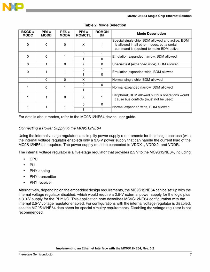
For details about modes, refer to the MC9S12NE64 device user guide.
Connecting a Power Supply to the MC9S12NE64
Using the internal voltage regulator can simplify power supply requirements for the design because (with the internal voltage regulator enabled) only a 3.3-V power supply that can handle the current load of the MC9S12NE64 is required. The power supply must be connected to VDDX1, VDDX2, and VDDR.
The internal voltage regulator is a five-stage regulator that provides 2.5 V to the MC9S12NE64, including:
• CPU
• PLL
• PHY analog
• PHY transmitter
• PHY receiver
Alternatively, depending on the embedded design requirements, the MC9S12NE64 can be set up with the internal voltage regulator disabled, which would require a 2.5-V external power supply for the logic plus a 3.3-V supply for the PHY I/O. This application note describes MC9S12NE64 configuration with the internal 2.5-V voltage regulator enabled. For configurations with the internal voltage regulator is disabled, see the MC9S12NE64 data sheet for special circuitry requirements. Disabling the voltage regulator is not recommended.
Table 2. Mode Selection
BKGD =MODC
PE6 =MODB
PE5 =MODA
PP6 =ROMCTL
ROMONBit Mode Description
0 0 0 X 1Special single chip, BDM allowed and active. BDM
is allowed in all other modes, but a serial command is required to make BDM active.
0 0 10 1
Emulation expanded narrow, BDM allowed1 0
0 1 0 X 0 Special test (expanded wide), BDM allowed
0 1 10 1
Emulation expanded wide, BDM allowed1 0
1 0 0 X 1 Normal single chip, BDM allowed
1 0 10 0
Normal expanded narrow, BDM allowed1 1
1 1 0 X 1Peripheral; BDM allowed but bus operations would
cause bus conflicts (must not be used)
1 1 10 0
Normal expanded wide, BDM allowed1 1
Implementing an Ethernet Interface with the MC9S12NE64, Rev. 0.2
Freescale Semiconductor 7

MC9S12NE64 Single-Chip Ethernet Solution
Connecting a Crystal to the MC9S12NE64
For basic operation of the MC9S12NE64 Ethernet controller, a 25-MHz crystal input with a tolerance of 25 ppm is required per IEEE 802.3 specification. The 25-MHz crystal input is required to provide the clock input to the integrated PHY for basic operation at 10 Mbps and/or 100 Mbps. The crystal must connect to the MC9S12NE64 in a Pierce configuration by the XTAL and EXTAL pins as shown on Table 5 with related cap and resistors.
In addition to providing a 25-MHz crystal input, to operate at 100 Mbps, the internal bus clock must be configured to 25 MHz. With the 25-MHz crystal, the CRG must be configured so the PLL is enabled and multiplies the crystal oscillator clock to achieve the internal bus clock 25 MHz operational setting.
For 10 Mbps, an internal bus clock setting of 2.5 MHz minimum is acceptable, but a 25-MHz crystal input is still required.
For details about the CRG and configuring the PLL, see Freescale Semiconductor document AN2692/D: MC9S12NE64 Integrated Ethernet Controller.
MC9S12NE64 PHY External Pins
Table 3 describes the pins related to the MC9S12NE64 PHY, their operation, and their circuitry design. The PHY pins in Table 3 serve several possible functions including power, signaling, component, and indicators for the EPHY.
Implementing an Ethernet Interface with the MC9S12NE64, Rev. 0.2
8 Freescale Semiconductor
MC9S12NE64 Single-Chip Ethernet Solution
Pi
r
(
NO1.
.
LED Indicator Pins
The power, signaling, and EPHY bias pins are required for basic operation of the EPHY; indicator pins (PL0:5) are optional. The EPHY can be configuring by software to drive indicator pins (PL0:5) automatically by setting the LEDEN bit of the EPHY EPHYCTL0 register. When LEDEN = 1, PL0:5 pins are dedicated to the EPHY. Alternatively, the system can be designed such that user software drives LEDs on any port pin to show EPHY status. For instance, the user may desire to show only link status. In this case, the user can manually drive an LED with software to show link status (with LEDEN bit = 0), which would allow the other four pins to be used for other purposes.
MC9S12NE64 low-level Ethernet drivers are available to handle software-driven LEDs.
Table 3. MC9S12NE64 PHY External Pins
n Function Pin Label(s) Pin Overview Description
Power
PHY_VDDA, PHY_VSSA
Power supply pins for EPHY analog power
This 2.5-V supply is derived from the internal voltage regulator. Nostatic load is allowed on these pins. The internal voltage regulatois turned off if VDDR is tied to ground.
PHY_VDDRX, PHY_VSSRX
Power supply pins for EPHY receiver power
PHY_VDDTX, PHY_VSSTX
Power supply pins for EPHY transmitter
Signaling
PHY_TXPEPHY twisted
pair output +
Ethernet twisted pair output pin. These pins are Hi-Z out of reset.PHY_TXN
EPHY twisted pair output –
PHY_RXPEPHY twisted
pair input +
PHY_RXNEPHY twisted
pair input –
CircuitEPHY bias
pin)PHY_RBIAS
EPHY bias control resistor
Connect an external bias resistor(1), (R5), between the PHY_RBIASpin and analog ground. This resistor should be placed as near a possible to the MCU pin. Stray capacitance must be less than 10pF (greater than 50 pF may cause instability). No high-speed signals should go in the region of the bias resistor.
TES: See the MC9S12NE64 data sheet for the value of the bias resistor
Indicator
COLLED Collision LEDFlashes in half-duplex mode when a collision occurs on the
network.
DUPLED Duplex LEDIndicates the duplex of the link, which can be full-duplex or half-
duplex.
SPDLED Speed LED Indicates the speed of a link, which can be 10 Mbps or 100 Mbps.
LNKLED Link LED Indicates whether a link is established with another network device
ACTLED Activity LED Flashes when data is received by the device.
Implementing an Ethernet Interface with the MC9S12NE64, Rev. 0.2
Freescale Semiconductor 9
MC9S12NE64 Single-Chip Ethernet Solution
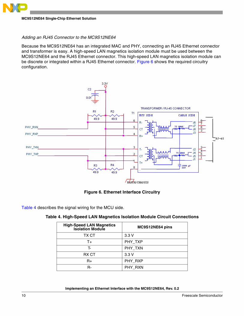
Adding an RJ45 Connector to the MC9S12NE64
Because the MC9S12NE64 has an integrated MAC and PHY, connecting an RJ45 Ethernet connector and transformer is easy. A high-speed LAN magnetics isolation module must be used between the MC9S12NE64 and the RJ45 Ethernet connector. This high-speed LAN magnetics isolation module can be discrete or integrated within a RJ45 Ethernet connector. Figure 6 shows the required circuitry configuration.
Figure 6. Ethernet Interface Circuitry
Table 4 describes the signal wiring for the MCU side.
Table 4. High-Speed LAN Magnetics Isolation Module Circuit Connections
High-Speed LAN Magnetics Isolation Module MC9S12NE64 pins
TX CT 3.3 V
T+ PHY_TXP
T- PHY_TXN
RX CT 3.3 V
R+ PHY_RXP
R- PHY_RXN
Implementing an Ethernet Interface with the MC9S12NE64, Rev. 0.2
10 Freescale Semiconductor
PCB Design Recommendation
PCB Design Recommendation
The section provides recommendations for PCB design and high-speed LAN magnetics isolation module selection.
General PCB Design Recommendations
The PCB layout must be designed to ensure proper operation of the voltage regulator and the MCU. The following recommendations are provided to ensure a robust PCB design:
• Every supply pair must be decoupled by a low-ESR (equivalent series resistance) ceramic capacitor connected as near as possible to the corresponding pins.
• Central point of the ground star should be the VSSX1 and VSSX2 pins.
• Use low-ohmic, low-inductance connections with VSS1, VSS2, VSSX1, and VSSX2 pins.
• VSSPLL must be directly connected to VSSX.
• Keep traces of VSSPLL, EXTAL, and XTAL as short as possible and their occupied board area as small as possible.
Ethernet PCB Design Recommendations
When designing a PCB that uses the MC9S12NE64 Ethernet module, several design considerations must be made to ensure that Ethernet operation conforms to the IEEE 802.3 physical interface specification. Use the following recommendations for PCB design between the high-speed LAN magnetics isolation module and:
• MC9S12NE64 EPHY external pins (most critical)
• RJ45 connector
Ethernet PCB design recommendations:
• The distance between the magnetic module and the RJ-45 jack is the most critical and must always be as short as possible (must be less than one inch).
• Never use 90° traces. Use 45° angles or radius curves in traces.
• Trace widths of 0.010” are recommended. Wider is better. Trace widths should not vary.
• Route differential Tx and Rx pairs near together (max 0.010” separation with 0.010” traces).
• Trace lengths must always be as short as possible (must be less than one inch).
• Make trace lengths as equal as possible.
• Keep TX and RX differential pairs routes separated (at least 0.020” separation). Better to separate with a ground plane.
• Avoid routing Tx and Rx traces over or under a plane. Areas under the Tx and Rx traces should be open, See Figures 9, 10, 11, 17 and 18.
• Use precision components in the line termination circuitry with 1% tolerance.
• Ensure that the power supply is rated for a load of 300 mA minimum.
• Avoid vias and layer changes.
Implementing an Ethernet Interface with the MC9S12NE64, Rev. 0.2
Freescale Semiconductor 11

PCB Design Recommendation
In addition, all termination resistors should be near to the driving source. The MCU is the driving source for PHY_TXP and PHY_TXN pins. The high-speed LAN magnetics isolation module is the driving source for PHY_RXP and PHY_RXN pins.
High-Speed LAN Magnetics Isolation Module Requirements
The MC9S12NE64 requires a 1:1 ratio transformer for the high-speed LAN magnetics isolation module for both the receive and the transmit signals. The basic high-speed LAN magnetics isolation module specification requirements are provided in Table 5. High-speed LAN magnetics isolation modules that meet these requirements are available from a variety of manufacturers.
The MC9S12NE64 can be used with high-speed LAN magnetics isolation modules that are either discrete or integrated into a RJ45 connector. Some of these integrated connectors have built-in LEDs as well. For the MC9S12NE64, an RJ45 connector with an integrated high-speed LAN magnetics isolation module is recommended because it reduces component count and simplifies PCB layout.
Because the MC9S12NE64 does not implement Auto-MDIX, an Auto-MDIX capable high-speed LAN magnetics isolation module is not required. A high-speed LAN magnetics isolation module with improved return loss characteristics is recommended to avoid Ethernet return loss issues.
Table 6 provides discrete and integrated high-speed LAN magnetics isolation modules that have been found in testing to satisfy the requirements necessary to establish an IEEE-compliant Ethernet interface with the MC9S12NE64. Other models can be used as long as the high-speed LAN magnetics isolation module specifications satisfy the requirements.
Although specific hardware is discussed in this section, Freescale Semiconductor does not recommend or endorse any particular product or vendor. This data is provided only to describe the specification requirements.
Table 5. High-Speed LAN Magnetics Isolation Module Specification Requirements
Parameter Value Units Test Condition
Tx/Rx turns ratio 1:1 CT / 1:1 — —
Inductance 350 mH (min) —
Insertion loss 1.1 dB (max) 1 to 100 MHz
Return loss
–18 dB (min) 1 to 30 MHz
–14 dB (min) 30 to 60 MHz
–12 dB (min) 60 to 80 MHz
Differential to common mode rejection
–40 dB (min) 1 to 60 MHz
–30 dB (min) 60 to 100 MHz
Transformer 1500 V —
Implementing an Ethernet Interface with the MC9S12NE64, Rev. 0.2
12 Freescale Semiconductor

Design Examples
Design Examples
This section shows two MC9S12NE64 design examples of Ethernet interface implementations with the MC9S12NE64 in a minimum system. These minimum system examples are provided only to demonstrate recommended MC9S12NE64 PCB design. These MC9S12NE64 design examples are test boards, and they are not available for purchase.
The first design shows a minimum system using the MC9S12NE64 in a 112-pin package. The second design is an example of a system using the 80-pin MC9S12NE64 with a very compact PCB footprint.
Schematics and all artwork layer views for both designs will be shown in this section. Both designs are implemented on 4-layer PCBs to provide better heat dissipation. Both boards are minimum system designs that use the internal voltage regulator.
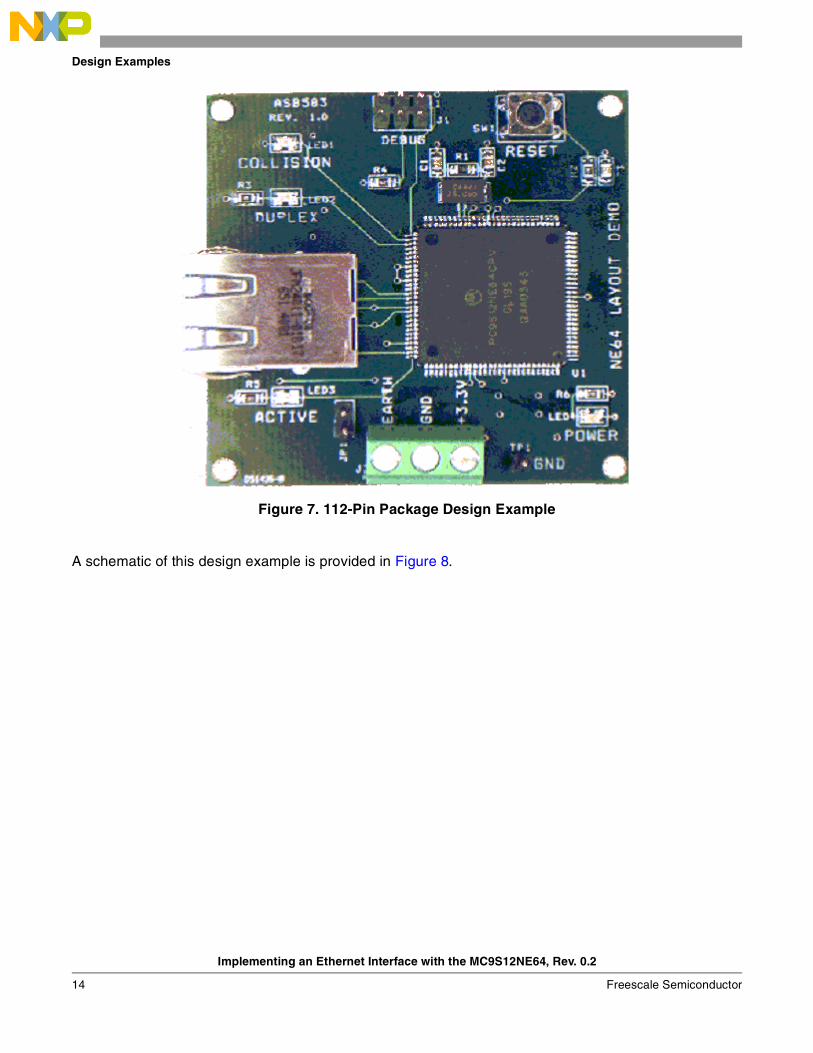
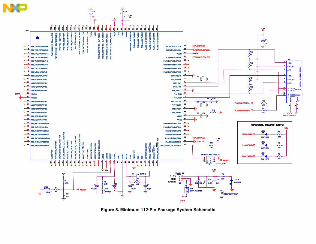
MC9S12NE64 112-Pin Package Design Example
A photo of the MC9S12NE64 112-pin package design example is provided in Figure 7. The PCB, which is approximately 6.3 cm x 6.3 cm, was designed using the recommendations discussed in the PCB Design Recommendation section. This design and PCB layout are discussed in detail in following sections.
Table 6. Discrete High-Speed LAN Magnetics Isolation Module
Type Manufacturer Model
DiscretePulse H1102
Midcom 000-6241-37R
Integrated
Pulse J10-0026
Midcom JFM25xxx-0510, JFM24xxx-1010
Bel Fuse 0810-1X1T-06
Halo HFJ11-2450E
Implementing an Ethernet Interface with the MC9S12NE64, Rev. 0.2
Freescale Semiconductor 13
Design Examples
Figure 7. 112-Pin Package Design Example
A schematic of this design example is provided in Figure 8.
Implementing an Ethernet Interface with the MC9S12NE64, Rev. 0.2
14 Freescale Semiconductor
R5
220
R850
EARTH/CHASSIS
PL4/COLLED
LED/LEDS
3.3V
3.3V
R15
330
R1450
R7
220
PL0/ACTLED
R1150
R3
220
LED1
COL_LED
R1250
C4
0.01
OPTIONAL STATUS LED's
TX+
TX_CT
TX-
RX+
RX_CT
RX-
CASE
ERTH
MIDCOM JFM2411-0101W
LED1ALED1C
LED2ALED2C
YELLOW
GREEN
J2
1
3
2
8
5
4
6
9 10
1413
1211
1
3
2
8
5
4
6
9 10
1413
1211
PL3/DUPLED
R13
330
LED2
DUP_LED
LED/LEDL
LED3
ACT_LED
R5
220
R850
EARTH/CHASSIS
R5
220
R850
EARTH/CHASSIS
PL4/COLLED
LED/LEDS
3.3V
3.3V
R15
330
R1450
R7
220PL4/COLLED
LED/LEDS
3.3V
3.3V
R15
330
R1450
R7
220
PL0/ACTLED
R1150
PL0/ACTLED
R1150
R3
220
LED1
COL_LED
R1250
C4
0.01
R3
220
LED1
COL_LED
R1250
C4
0.01
OPTIONAL STATUS LED's
TX+
TX_CT
TX-
RX+
RX_CT
RX-
CASE
ERTH
MIDCOM JFM2411-0101W
LED1ALED1C
LED2ALED2C
YELLOW
GREEN
J2
1
3
2
8
5
4
6
9 10
1413
1211
1
3
2
8
5
4
6
9 10
1413
1211
PL3/DUPLED
R13
330
LED2
DUP_LED
LED/LEDL
LED3
ACT_LED
OPTIONAL STATUS LED's
TX+
TX_CT
TX-
RX+
RX_CT
RX-
CASE
ERTH
MIDCOM JFM2411-0101W
LED1ALED1C
LED2ALED2C
YELLOW
GREEN
J2
1
3
2
8
5
4
6
9 10
1413
1211
1
3
2
8
5
4
6
9 10
1413
1211
PL3/DUPLED
R13
330
LED2
DUP_LED
LED/LEDL
LED3
ACT_LED
Figure 8. Minimum 112-Pin Package System Schematic
C3
0.22
3.3V
PL3/DUPLED
3.3V
3.3V
C9.22
C5
0.1*RESET
R1
10M
3.3V
R427k
TP1
GND TESTPOINT
11
+
C16 100 uF
PL2/SPD
J1
BACKGROUND DEBUG
135
246
135
246
C13
.1
EARTH
R6
330
C6.22
*RESET
PL0/ACTLED
R2
47
U1
1
2
3
4
5
6
7
8
9
10
11
12
13
14
15
16
17
18
19
20
21
22
23
24
25
26
27
28
29 30 31 32 33 34 35 36 37 38 39 40 41 42 43 44 45 46 47 48 49 50 51 52 53 54 55 56
57
58
59
60
61
62
63
64
65
66
67
68
69
70
71
72
73
74
75
76
77
78
79
80
81
82
83
84
858687888990919293949596979899100
101
102
103
104
105
106
107
108
109
110
111
112
MII_TXER/KWH6/PH6
MII_TXEN/KWH5/PH5
MII_TXCLK/KWH4/PH4
MII_TXD3/KWH3/PH3
MII_TXD2/KWH2/PH2
MII_TXD1/KWH1/PH1
MII_TXD0/KWH0/PH0
MII_MDC/KWJ0/PJ0
MII_MDIO/KWJ1/PJ1
ADDR0/DATA0/PB0
ADDR1/DATA1/PB1
ADDR2/DATA2/PB2
ADDR3/DATA3/PB3
VDDX1
VSSX1
ADDR4/DATA4/PB4
ADDR5/DATA5/PB5
ADDR6/DATA6/PB6
ADDR7/DATA7/PB7
MII_CRS/KWJ6/PJ2
MII_COL/KWJ7/PJ3
MII_RXD0/KWG0/PG0
MII_RXD1/KWG1/PG1
MII_RXD2/KWG2/PG2
MII_RXD3/KWG3/PG3
MII_RXCLK/KWG4/PG4
MII_RXDV/KWG5/PG5
MII_RXER/KWG6/PG6
KW
G7/
PG
7
PH
Y4/
SC
I0_
RX
D/ P
S0
DIS
AB
LE10
0/ S
CI0
_ T
XD
/ PS
1
SC
AN
_ E
NA
BLE
/ S
CI1
_ R
XD
/ PS
2
RX
D4/
SC
I1_
TX
D/
PS
3
TX
D4/
SP
I_ M
ISO
/ PS
4
SC
AN
_ S
ET
/ SP
I_ M
OS
I/ P
S5
SC
AN
_ R
ES
ET
/ SP
I_ S
CK
/ PS
6
MD
INT
/ SP
I_ S
S/ P
S7
NO
AC
C/ P
E7
MO
DB
/ IP
IPE
1/ P
E6
MO
DA
/ IP
IPE
0/ P
E5
SC
AN
CLK
1/ E
CLK
/ PE
4
VS
SX
2
VD
DX
2
RE
SE
T
VD
DP
LL
XFC
VS
SP
LL
EX
TA
L
XT
AL
TE
ST
/ VP
P
PL6
PL5
LST
RB
/TA
GLO
/PE
3
AN
LG_T
ST
/R/W
/PE
2
SID
DQ
/ IR
Q/ P
E1
SC
AN
_ M
OD
E/ X
IRQ
/ P
E0
BKGD/MODC/SCANCLK2
PL4/COLLED/LEDC
PL3/DUPLED/LEDD
PA0/ADDR8/DATA8
PA1/ADDR9/DATA9
PA2/ADDR10/DATA10
PA3/ADDR11/DATA11
VSS2
VDD2
PHY_RBIAS
PHY_VSSA
PHY_VDDA
PHY_VDDTX
PHY_TXP
PHY_TXN
PHY_VSSTX
PHY_RXP
PHY_RXN
PHY_VDDRX
PHY_VSSRX
PA4/ADDR12/DATA12
PA5/ADDR13/DATA13
PA6/ADDR14/DATA14
PA7/ADDR15/DATA15
PL2/SPDLED/LEDS
VDDR
PL1/LNKLED/LEDL
PL0/ACTLED/LEDT
PA
D0/
AN
0/ B
GT
RIM
0
PA
D1/
AN
1/ B
GT
RIM
1
PA
D2/
AN
2/ B
GT
RIM
2
PA
D3/
AN
3/ B
GT
RIM
3
PA
D4/
AN
4/ T
MO
D0
PA
D5/
AN
5/ T
MO
D1
PA
D6/
AN
6/ T
MO
D2
PA
D7/
AN
7/ S
CA
NC
LK3
VD
DA
VR
H
VR
L
VS
SA
PK
0/ X
AD
DR
14/ T
X_
AM
P_
TR
IM0
PK
1/ X
AD
DR
15/ T
X_
AM
P_
TR
IM1
PK
2/ X
AD
DR
16/ T
X_
SLP
_ T
RIM
0
PK
3/ X
AD
DR
17/ T
X_
SLP
_ T
RIM
1
VS
S1
VD
D1
PK
4/ X
AD
DR
18/ B
10_
DIS
PK
5/ X
AD
DR
19/ B
100_
DIS
PK
6/ X
CS
/ SY
MB
OL_
MO
DE
PK
7/ E
CS
/ TR
IST
AT
E
PT
7/ T
IM_
IOC
7/ P
HY
3
PT
6/ T
IM_
IOC
6/ P
HY
2
PT
5/ T
IM_
IOC
5/ P
HY
1
PT
4/ T
IM_
IOC
4/ P
HY
0
PJ7
/ KW
J7/ I
IC_
SC
L/ D
ISA
BLE
10
PJ6
/ KW
J6/ I
IC_
SD
A/ A
ND
IS
C10.22
C7
470 pF
Y1 25 MHz
3.3V
JP12-PIN JUMPER
12
12
R16
10k
PL2/SPDLED/LEDS
SW1
RESET
GND LED4
POWERC1
15 pF
J3
POWER_IN
123
123
C11.22
R92.2k
3.3V
C15
0.01
C12
.22
C2
15 pFC8
4700 pF
3.3V
R10
PL4/COLLED
3.3V
C14
0.22
PL1/LNKLED/LEDL
PL1/LNK
3.3V
C3
0.22
3.3V
PL3/DUPLED
3.3V
3.3V
C9.22
C5
0.1*RESET
R1
10M
3.3V
R427k
TP1
GND TESTPOINT
11
+
C16 100 uF
C3
0.22
3.3V
PL3/DUPLED
3.3V
3.3V
C9.22
C5
0.1*RESET
R1
10M
3.3V
R427k
TP1
GND TESTPOINT
11
+
C16 100 uF
PL2/SPD
J1
BACKGROUND DEBUG
135
246
135
246
C13
.1
EARTH
R6
330
C6.22
*RESET
PL0/ACTLED
R2
47
PL2/SPD
J1
BACKGROUND DEBUG
135
246
135
246
C13
.1
EARTH
R6
330
C6.22
*RESET
PL0/ACTLED
R2
47
U1
1
2
3
4
5
6
7
8
9
10
11
12
13
14
15
16
17
18
19
20
21
22
23
24
25
26
27
28
29 30 31 32 33 34 35 36 37 38 39 40 41 42 43 44 45 46 47 48 49 50 51 52 53 54 55 56
57
58
59
60
61
62
63
64
65
66
67
68
69
70
71
72
73
74
75
76
77
78
79
80
81
82
83
84
8586878889909192939495
U1
1
2
3
4
5
6
7
8
9
10
11
12
13
14
15
16
17
18
19
20
21
22
23
24
25
26
27
28
29 30 31 32 33 34 35 36 37 38 39 40 41 42 43 44 45 46 47 48 49 50 51 52 53 54 55 56
57
58
59
60
61
62
63
64
65
66
67
68
69
70
71
72
73
74
75
76
77
78
79
80
81
82
83
84
858687888990919293949596979899100
101
102
103
104
105
106
107
108
109
110
111
112
MII_TXER/KWH6/PH6
MII_TXEN/KWH5/PH5
MII_TXCLK/KWH4/PH4
MII_TXD3/KWH3/PH3
MII_TXD2/KWH2/PH2
MII_TXD1/KWH1/PH1
MII_TXD0/KWH0/PH0
MII_MDC/KWJ0/PJ0
MII_MDIO/KWJ1/PJ1
ADDR0/DATA0/PB0
ADDR1/DATA1/PB1
ADDR2/DATA2/PB2
ADDR3/DATA3/PB3
VDDX1
VSSX1
ADDR4/DATA4/PB4
ADDR5/DATA5/PB5
ADDR6/DATA6/PB6
ADDR7/DATA7/PB7
MII_CRS/KWJ6/PJ2
MII_COL/KWJ7/PJ3
MII_RXD0/KWG0/PG0
MII_RXD1/KWG1/PG1
MII_RXD2/KWG2/PG2
MII_RXD3/KWG3/PG3
MII_RXCLK/KWG4/PG4
MII_RXDV/KWG5/PG5
MII_RXER/KWG6/PG6
KW
G7/
PG
7
PH
Y4/
SC
I0_
RX
D/ P
S0
DIS
AB
LE10
0/ S
CI0
_ T
XD
/ PS
1
SC
AN
_ E
NA
BLE
/ S
CI1
_ R
XD
/ PS
2
RX
D4/
SC
I1_
TX
D/
PS
3
TX
D4/
SP
I_ M
ISO
/ PS
4
SC
AN
_ S
ET
/ SP
I_ M
OS
I/ P
S5
SC
AN
_ R
ES
ET
/ SP
I_ S
CK
/ PS
6
MD
INT
/ SP
I_ S
S/ P
S7
NO
AC
C/ P
E7
MO
DB
/ IP
IPE
1/ P
E6
MO
DA
/ IP
IPE
0/ P
E5
SC
AN
CLK
1/ E
CLK
/ PE
4
VS
SX
2
VD
DX
2
RE
SE
T
VD
DP
LL
XFC
VS
SP
LL
EX
TA
L
XT
AL
TE
ST
/ VP
P
PL6
PL5
LST
RB
/TA
GLO
/PE
3
AN
LG_T
ST
/R/W
/PE
2
SID
DQ
/ IR
Q/ P
E1
SC
AN
_ M
OD
E/ X
IRQ
/ P
E0
BKGD/MODC/SCANCLK2
PL4/COLLED/LEDC
PL3/DUPLED/LEDD
PA0/ADDR8/DATA8
PA1/ADDR9/DATA9
PA2/ADDR10/DATA10
PA3/ADDR11/DATA11
VSS2
VDD2
PHY_RBIAS
PHY_VSSA
PHY_VDDA
PHY_VDDTX
PHY_TXP
PHY_TXN
PHY_VSSTX
PHY_RXP
PHY_RXN
PHY_VDDRX
PHY_VSSRX
PA4/ADDR12/DATA12
PA5/ADDR13/DATA13
PA6/ADDR14/DATA14
PA7/ADDR15/DATA15
PL2/SPDLED/LEDS
VDDR
PL1/LNKLED/LEDL
PL0/ACTLED/LEDT
PA
D0/
AN
0/ B
GT
RIM
0
PA
D1/
AN
1/ B
GT
RIM
1
PA
D2/
AN
2/ B
GT
RIM
2
PA
D3/
AN
3/ B
GT
RIM
3
PA
D4/
AN
4/ T
MO
D0
PA
D5/
AN
5/ T
MO
D1
PA
D6/
AN
6/ T
MO
D2
PA
D7/
AN
7/ S
CA
NC
LK3
VD
DA
VR
H
VR
L
VS
SA
PK
0/ X
AD
DR
14/ T
X_
AM
P_
TR
IM0
PK
1/ X
AD
DR
15/ T
X_
AM
P_
TR
IM1
PK
2/ X
AD
DR
16/ T
X_
SLP
_ T
RIM
0
PK
3/ X
AD
DR
17/ T
X_
SLP
_ T
RIM
1
VS
S1
VD
D1
PK
4/ X
AD
DR
18/ B
10_
DIS
PK
5/ X
AD
DR
19/ B
100_
DIS
PK
6/ X
CS
/ SY
MB
OL_
MO
DE
PK
7/ E
CS
/ TR
IST
AT
E
PT
7/ T
IM_
IOC
7/ P
HY
3
PT
6/ T
IM_
IOC
6/ P
HY
2
PT
5/ T
IM_
IOC
5/ P
HY
1
PT
4/ T
IM_
IOC
4/ P
HY
0
PJ7
/ KW
J7/ I
IC_
SC
L/ D
ISA
BLE
10
PJ6
/ KW
J6/ I
IC_
SD
A/ A
ND
IS
96979899100
101
102
103
104
105
106
107
108
109
110
111
112
MII_TXER/KWH6/PH6
MII_TXEN/KWH5/PH5
MII_TXCLK/KWH4/PH4
MII_TXD3/KWH3/PH3
MII_TXD2/KWH2/PH2
MII_TXD1/KWH1/PH1
MII_TXD0/KWH0/PH0
MII_MDC/KWJ0/PJ0
MII_MDIO/KWJ1/PJ1
ADDR0/DATA0/PB0
ADDR1/DATA1/PB1
ADDR2/DATA2/PB2
ADDR3/DATA3/PB3
VDDX1
VSSX1
ADDR4/DATA4/PB4
ADDR5/DATA5/PB5
ADDR6/DATA6/PB6
ADDR7/DATA7/PB7
MII_CRS/KWJ6/PJ2
MII_COL/KWJ7/PJ3
MII_RXD0/KWG0/PG0
MII_RXD1/KWG1/PG1
MII_RXD2/KWG2/PG2
MII_RXD3/KWG3/PG3
MII_RXCLK/KWG4/PG4
MII_RXDV/KWG5/PG5
MII_RXER/KWG6/PG6
KW
G7/
PG
7
PH
Y4/
SC
I0_
RX
D/ P
S0
DIS
AB
LE10
0/ S
CI0
_ T
XD
/ PS
1
SC
AN
_ E
NA
BLE
/ S
CI1
_ R
XD
/ PS
2
RX
D4/
SC
I1_
TX
D/
PS
3
TX
D4/
SP
I_ M
ISO
/ PS
4
SC
AN
_ S
ET
/ SP
I_ M
OS
I/ P
S5
SC
AN
_ R
ES
ET
/ SP
I_ S
CK
/ PS
6
MD
INT
/ SP
I_ S
S/ P
S7
NO
AC
C/ P
E7
MO
DB
/ IP
IPE
1/ P
E6
MO
DA
/ IP
IPE
0/ P
E5
SC
AN
CLK
1/ E
CLK
/ PE
4
VS
SX
2
VD
DX
2
RE
SE
T
VD
DP
LL
XFC
VS
SP
LL
EX
TA
L
XT
AL
TE
ST
/ VP
P
PL6
PL5
LST
RB
/TA
GLO
/PE
3
AN
LG_T
ST
/R/W
/PE
2
SID
DQ
/ IR
Q/ P
E1
SC
AN
_ M
OD
E/ X
IRQ
/ P
E0
BKGD/MODC/SCANCLK2
PL4/COLLED/LEDC
PL3/DUPLED/LEDD
PA0/ADDR8/DATA8
PA1/ADDR9/DATA9
PA2/ADDR10/DATA10
PA3/ADDR11/DATA11
VSS2
VDD2
PHY_RBIAS
PHY_VSSA
PHY_VDDA
PHY_VDDTX
PHY_TXP
PHY_TXN
PHY_VSSTX
PHY_RXP
PHY_RXN
PHY_VDDRX
PHY_VSSRX
PA4/ADDR12/DATA12
PA5/ADDR13/DATA13
PA6/ADDR14/DATA14
PA7/ADDR15/DATA15
PL2/SPDLED/LEDS
VDDR
PL1/LNKLED/LEDL
PL0/ACTLED/LEDT
PA
D0/
AN
0/ B
GT
RIM
0
PA
D1/
AN
1/ B
GT
RIM
1
PA
D2/
AN
2/ B
GT
RIM
2
PA
D3/
AN
3/ B
GT
RIM
3
PA
D4/
AN
4/ T
MO
D0
PA
D5/
AN
5/ T
MO
D1
PA
D6/
AN
6/ T
MO
D2
PA
D7/
AN
7/ S
CA
NC
LK3
VD
DA
VR
H
VR
L
VS
SA
PK
0/ X
AD
DR
14/ T
X_
AM
P_
TR
IM0
PK
1/ X
AD
DR
15/ T
X_
AM
P_
TR
IM1
PK
2/ X
AD
DR
16/ T
X_
SLP
_ T
RIM
0
PK
3/ X
AD
DR
17/ T
X_
SLP
_ T
RIM
1
VS
S1
VD
D1
PK
4/ X
AD
DR
18/ B
10_
DIS
PK
5/ X
AD
DR
19/ B
100_
DIS
PK
6/ X
CS
/ SY
MB
OL_
MO
DE
PK
7/ E
CS
/ TR
IST
AT
E
PT
7/ T
IM_
IOC
7/ P
HY
3
PT
6/ T
IM_
IOC
6/ P
HY
2
PT
5/ T
IM_
IOC
5/ P
HY
1
PT
4/ T
IM_
IOC
4/ P
HY
0
PJ7
/ KW
J7/ I
IC_
SC
L/ D
ISA
BLE
10
PJ6
/ KW
J6/ I
IC_
SD
A/ A
ND
IS
C10.22
C7
470 pF
Y1 25 MHz
3.3V
JP12-PIN JUMPER
12
12
R16
10k
C10.22
C7
470 pF
Y1 25 MHz
3.3V
JP12-PIN JUMPER
12
12
R16
10k
PL2/SPDLED/LEDS
SW1
RESET
GND LED4
POWERC1
15 pF
J3
POWER_IN
123
123
C11.22
R92.2k
3.3V
C15
0.01
C12
.22
C2
15 pFC8
4700 pF
3.3V
R10
PL2/SPDLED/LEDS
SW1
RESET
GND LED4
POWERC1
15 pF
J3
POWER_IN
123
123
C11.22
R92.2k
3.3V
C15
0.01
C12
.22
C2
15 pFC8
4700 pF
3.3V
R10
PL4/COLLED
3.3V
C14
0.22
PL1/LNKLED/LEDL
PL1/LNK
3.3V
PL4/COLLED
3.3V
C14
0.22
PL1/LNKLED/LEDL
PL1/LNK
3.3V
Design Examples
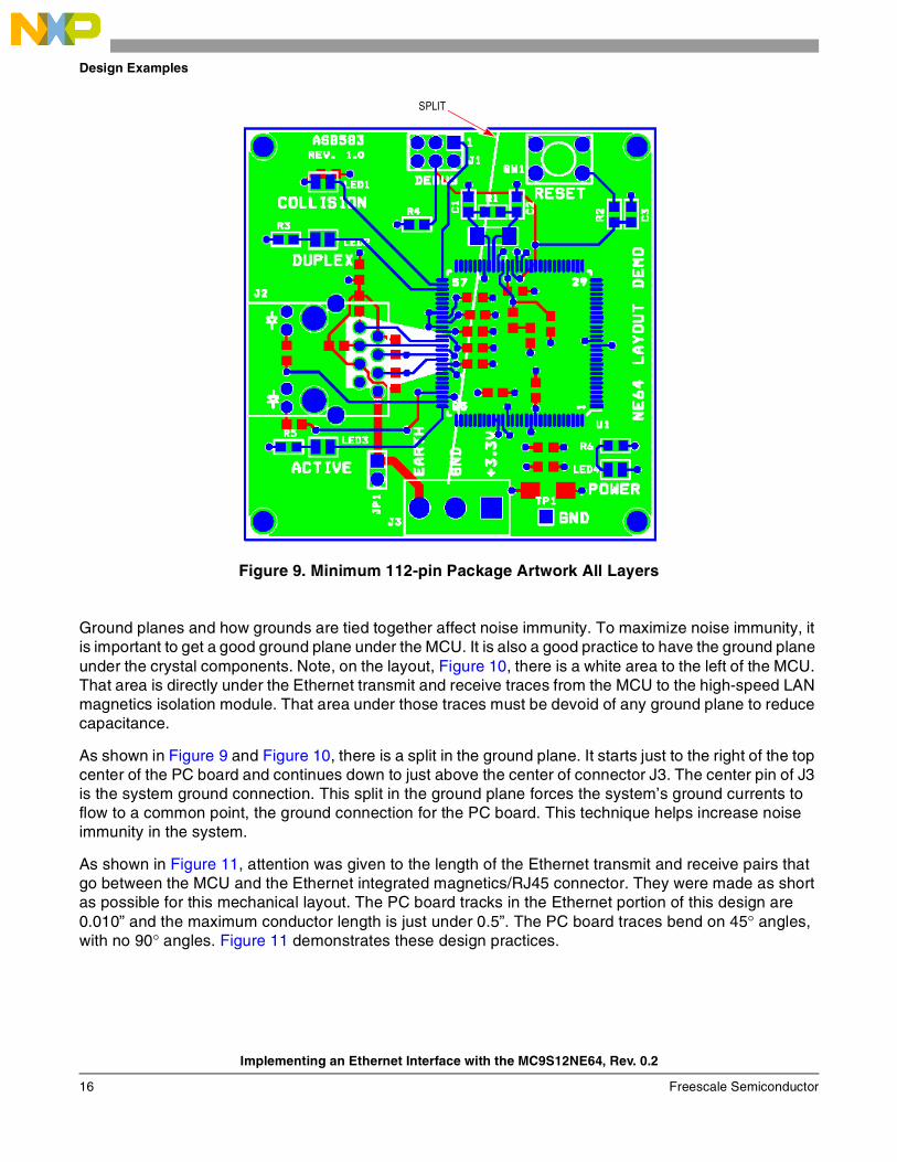
Figure 9. Minimum 112-pin Package Artwork All Layers
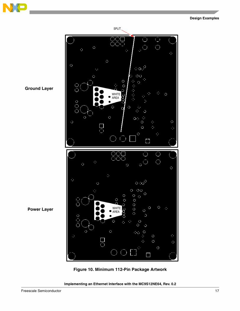
Ground planes and how grounds are tied together affect noise immunity. To maximize noise immunity, it is important to get a good ground plane under the MCU. It is also a good practice to have the ground plane under the crystal components. Note, on the layout, Figure 10, there is a white area to the left of the MCU. That area is directly under the Ethernet transmit and receive traces from the MCU to the high-speed LAN magnetics isolation module. That area under those traces must be devoid of any ground plane to reduce capacitance.
As shown in Figure 9 and Figure 10, there is a split in the ground plane. It starts just to the right of the top center of the PC board and continues down to just above the center of connector J3. The center pin of J3 is the system ground connection. This split in the ground plane forces the system’s ground currents to flow to a common point, the ground connection for the PC board. This technique helps increase noise immunity in the system.
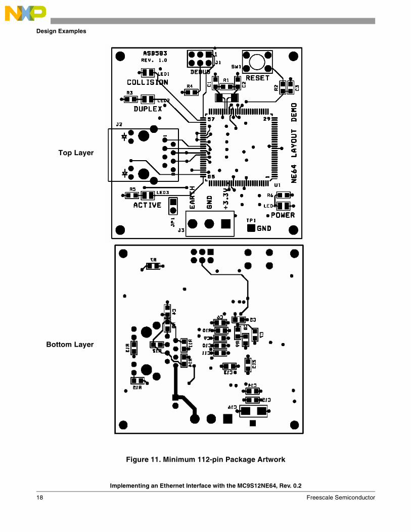
As shown in Figure 11, attention was given to the length of the Ethernet transmit and receive pairs that go between the MCU and the Ethernet integrated magnetics/RJ45 connector. They were made as short as possible for this mechanical layout. The PC board tracks in the Ethernet portion of this design are 0.010” and the maximum conductor length is just under 0.5”. The PC board traces bend on 45° angles, with no 90° angles. Figure 11 demonstrates these design practices.
SPLIT
Implementing an Ethernet Interface with the MC9S12NE64, Rev. 0.2
16 Freescale Semiconductor
Design Examples
Figure 10. Minimum 112-Pin Package Artwork
Ground Layer
SPLIT
WHITEAREA
WHITEAREA
Power Layer
Implementing an Ethernet Interface with the MC9S12NE64, Rev. 0.2
Freescale Semiconductor 17
Design Examples
Figure 11. Minimum 112-pin Package Artwork
Top Layer
Bottom Layer
Implementing an Ethernet Interface with the MC9S12NE64, Rev. 0.2
18 Freescale Semiconductor
Design Examples
As with all designs, place the crystal and its associated components as near to their MCU pins as possible and use minimum trace lengths. This is also true with the XFC connections (PLL components).
There are a number of power supply decoupling capacitors necessary to decouple the MCU and its various internal power supplies. These pins are VDD1, VDD2, VDDA, VDDPLL, PHY_VDDRX, and PHY_VDDTX. These capacitors should be good quality, low ESR type ceramic components.
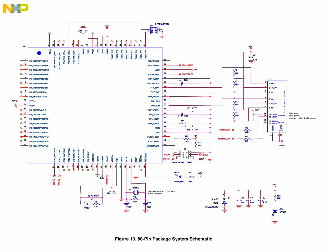
MC9S12NE64 80-Pin Package Design Example
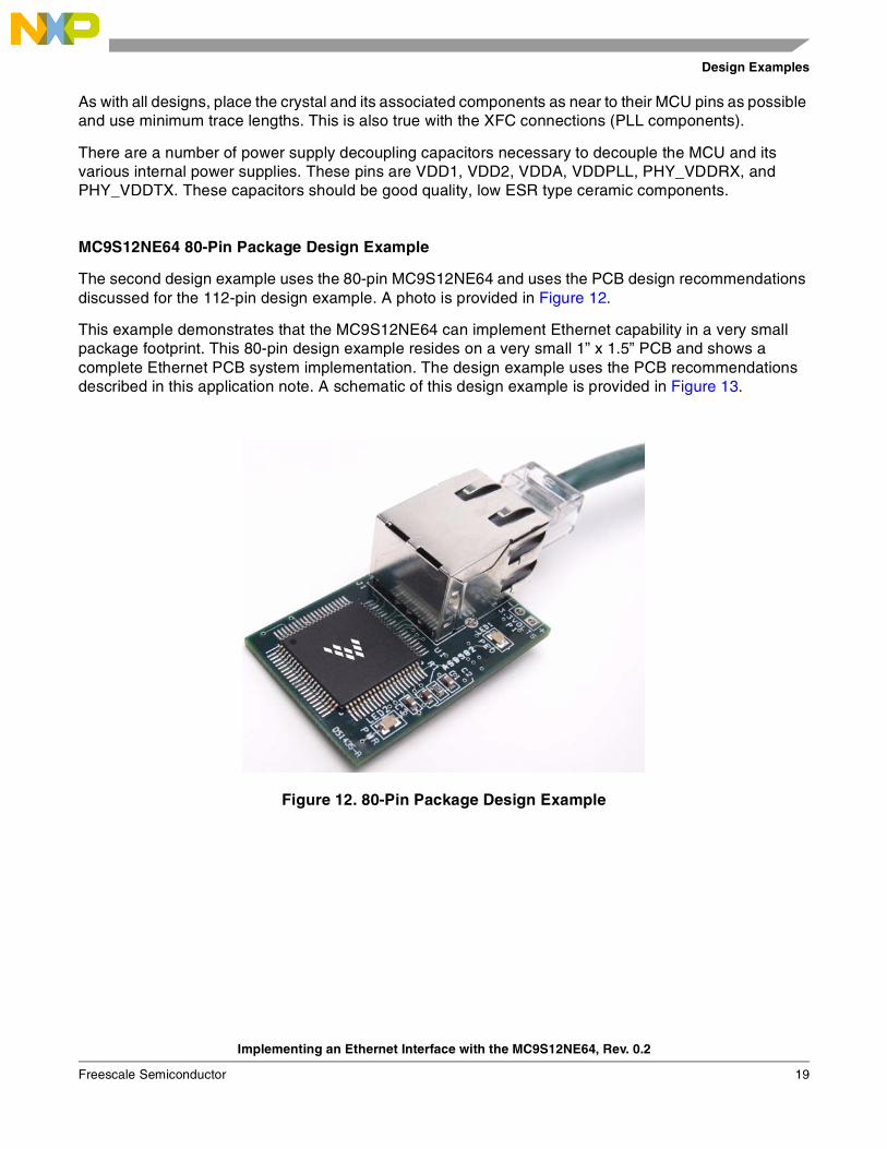
The second design example uses the 80-pin MC9S12NE64 and uses the PCB design recommendations discussed for the 112-pin design example. A photo is provided in Figure 12.
This example demonstrates that the MC9S12NE64 can implement Ethernet capability in a very small package footprint. This 80-pin design example resides on a very small 1” x 1.5” PCB and shows a complete Ethernet PCB system implementation. The design example uses the PCB recommendations described in this application note. A schematic of this design example is provided in Figure 13.
Figure 12. 80-Pin Package Design Example
Implementing an Ethernet Interface with the MC9S12NE64, Rev. 0.2
Freescale Semiconductor 19
TX+
TX_CT
TX-
RX+
RX_CT
RX-
CASE
ERTH
MIDCOM JFM2411-0101W
LED1ALED1C
LED2ALED2C
YELLOW
GREEN
J1
1
3
2
8
5
4
6
9 10
1413
1211
1
3
2
8
5
4
6
9 10
1413
1211
3.3V
3.3V
R11330
LED2
POWER
C7
0.01
C5
0.01
.3V
+C4
10 uF
lnk greenspd green
duplex = third LED green
TX+
TX_CT
TX-
RX+
RX_CT
RX-
CASE
ERTH
MIDCOM JFM2411-0101W
LED1ALED1C
LED2ALED2C
YELLOW
GREEN
J1
1
3
2
8
5
4
6
9 10
1413
1211
1
3
2
8
5
4
6
9 10
1413
1211
TX+
TX_CT
TX-
RX+
RX_CT
RX-
CASE
ERTH
MIDCOM JFM2411-0101W
LED1ALED1C
LED2ALED2C
YELLOW
GREEN
J1
1
3
2
8
5
4
6
9 10
1413
1211
1
3
2
8
5
4
6
9 10
1413
1211
3.3V
3.3V
R11330
3.3V
3.3V
R11330
LED2
POWER
C7
0.01
LED2
POWER
C7
0.01
C5
0.01
.3V
+C4
10 uF
C5
0.01
.3V
+C4
10 uF
lnk greenspd green
duplex = third LED green
Figure 13. 80-Pin Package System Schematic
3.3V
R7
49.9
R3
330
P22-PAD JUMPER
1 23 41 2
3 4
R1
2.2k
*RE
SE
T
C30.22
C12 0.22
Citizen page 627,top left300-8105-1-ND
3.3V
C11 0.22
C13
15pF
3.3V
Y125 MHz
U1
1
2
3
4
5
6
7
8
9
10
11
12
13
14
15
16
17
18
19
20
21 22 23 24 25 26 27 28 30 31 32 33 34 35 36 37 38 39 4041
42
43
44
45
46
47
48
49
50
51
52
53
54
55
56
57
58
59
60
6162636465666768697071727374757677787980
29
81
MII_TXER/KWH6/PH6
MII_TXEN/KWH5/PH5
MII_TXCLK/KWH4/PH4
MII_TXD3/KWH3/PH3
MII_TXD2/KWH2/PH2
MII_TXD1/KWH1/PH1
MII_TXD0/KWH0/PH0
MII_MDC/KWJ0/PJ0
MII_MDIO/KWJ1/PJ1
VDDX1
VSSX1
MII_CRS/KWJ6/PJ2
MII_COL/KWJ7/PJ3
MII_RXD0/KWG0/PG0
MII_RXD1/KWG1/PG1
MII_RXD2/KWG2/PG2
MII_RXD3/KWG3/PG3
MII_RXCLK/KWG4/PG4
MII_RXDV/KWG5/PG5
MII_RXER/KWG6/PG6
SC
I0_
RXD
/ PS
0
SC
I0_
TX
D/ P
S1
SC
I1_
RXD
/ PS
2
SC
I1_
TXD
/ PS
3
SP
I_ M
ISO
/ PS
4
SP
I_ M
OS
I/ P
S5
SP
I_ S
CK
/ P
S6
SP
I_S
S/ P
S7
VS
SX2
VD
DX2
RE
SE
T
VD
DP
LL
XFC
VS
SP
LL
EX
TA
L
XTA
L
TE
ST
IRQ
/ PE
1
XIR
Q/ P
E0
BKGD/MODC
PL4/COLLED
PL3/DUPLED
VSS2
VDD2
PHY_RBIAS
PHY_VSSA
PHY_VDDA
PHY_VDDTX
PHY_TXP
PHY_TXN
PHY_VSSTX
PHY_RXP
PHY_RXN
PHY_VDDRX
PHY_VSSRX
PL2/SPDLED
VDDR
PL1/LNKLED
PL0/ACTLED
PA
D0/
AN
0
PA
D1/
AN
1
PA
D2/
AN
2
PA
D3/
AN
3
PA
D4/
AN
4
PA
D5/
AN
5
PA
D6/
AN
6
PA
D7/
AN
7
VD
DA
VR
H
VR
L
VS
SA
VS
S1
VD
D1
PT7/
TIM
_ IO
C7
PT6/
TIM
_ IO
C6
PT5/
TIM
_ IO
C5
PT4/
TIM
_ IO
C4
PJ7
/ KW
J7/ I
IC_
SC
L
PJ6
/ KW
J6/ I
IC_S
DA
EC
LK/P
E4
FLA
G
PL1/LNKLED
R4
330
PL2/SPDLED
R10
10M
J2
BACKGROUND DEBUG
135
246
135
246
3.3V
SC
I_R
x
R12
10k
P1
2-PAD JUMPER
12
12
C8 0.22
R13
10k
C10
15pF
3.3V
C140.22
R5
49.9
C1
4700pF
LED1
USER_LED
PL1/LNKLED
*RESET
+3.3V C6
0.1
3
SC
I_T
x
SCI_Tx
3.3V
GND
3.3V
PL2/SPDLED
R2
330
C9 0.22
R9
12.4k 1%
R8
49.9
C2 470Pf
SCI_Rx
R6
49.9
3.3V
R7
49.9
R3
330
P22-PAD JUMPER
1 23 41 2
3 4
R1
2.2k
*RE
SE
T
C30.22
C12 0.22
Citizen page 627,top left300-8105-1-ND
3.3V
C11 0.22
C13
15pF
3.3V
Y125 MHz
3.3V
R7
49.9
R3
330
P22-PAD JUMPER
1 23 41 2
3 4
R1
2.2k
*RE
SE
T
C30.22
C12 0.22
Citizen page 627,top left300-8105-1-ND
3.3V
C11 0.22
C13
15pF
3.3V
Y125 MHz
U1
1
2
3
4
5
6
7
8
9
10
11
12
13
14
15
16
17
18
19
20
21 22 23 24 25 26 27 28 30 31 32 33 34 35 36 37 38 39 4041
42
43
44
45
46
47
48
49
50
51
52
53
54
55
56
57
58
59
60
6162636465666768697071727374757677787980
29
81
MII_TXER/KWH6/PH6
MII_TXEN/KWH5/PH5
MII_TXCLK/KWH4/PH4
MII_TXD3/KWH3/PH3
MII_TXD2/KWH2/PH2
MII_TXD1/KWH1/PH1
MII_TXD0/KWH0/PH0
MII_MDC/KWJ0/PJ0
MII_MDIO/KWJ1/PJ1
VDDX1
VSSX1
MII_CRS/KWJ6/PJ2
MII_COL/KWJ7/PJ3
MII_RXD0/KWG0/PG0
MII_RXD1/KWG1/PG1
MII_RXD2/KWG2/PG2
MII_RXD3/KWG3/PG3
MII_RXCLK/KWG4/PG4
MII_RXDV/KWG5/PG5
MII_RXER/KWG6/PG6
SC
I0_
RXD
/ PS
0
SC
I0_
TX
D/ P
S1
SC
I1_
RXD
/ PS
2
SC
I1_
TXD
/ PS
3
SP
I_ M
ISO
/ PS
4
SP
I_ M
OS
I/ P
S5
SP
I_ S
CK
/ P
S6
SP
I_S
S/ P
S7
VS
SX2
VD
DX2
RE
SE
T
VD
DP
LL
XFC
VS
SP
LL
EX
TA
L
XTA
L
TE
ST
IRQ
/ PE
1
XIR
Q/ P
E0
BKGD/MODC
PL4/COLLED
PL3/DUPLED
VSS2
VDD2
PHY_RBIAS
PHY_VSSA
PHY_VDDA
PHY_VDDTX
PHY_TXP
PHY_TXN
PHY_VSSTX
PHY_RXP
PHY_RXN
PHY_VDDRX
PHY_VSSRX
PL2/SPDLED
VDDR
PL1/LNKLED
PL0/ACTLED
PA
D0/
AN
0
PA
D1/
AN
1
PA
D2/
AN
2
PA
D3/
AN
3
PA
D4/
AN
4
PA
D5/
AN
5
PA
D6/
AN
6
PA
D7/
AN
7
VD
DA
VR
H
VR
L
VS
SA
VS
S1
VD
D1
PT7/
TIM
_ IO
C7
PT6/
TIM
_ IO
C6
PT5/
TIM
_ IO
C5
PT4/
TIM
_ IO
C4
PJ7
/ KW
J7/ I
IC_
SC
L
PJ6
/ KW
J6/ I
IC_S
DA
EC
LK/P
E4
FLA
G
PL1/LNKLED
R4
330
PL2/SPDLED
SP
I_S
S/ P
S7
VS
SX2
VD
DX2
RE
SE
T
VD
DP
LL
XFC
VS
SP
LL
EX
TA
L
XTA
L
TE
ST
IRQ
/ PE
1
XIR
Q/ P
E0
BKGD/MODC
PL4/COLLED
PL3/DUPLED
VSS2
VDD2
PHY_RBIAS
PHY_VSSA
PHY_VDDA
PHY_VDDTX
PHY_TXP
PHY_TXN
PHY_VSSTX
PHY_RXP
PHY_RXN
PHY_VDDRX
PHY_VSSRX
PL2/SPDLED
VDDR
PL1/LNKLED
PL0/ACTLED
PA
D0/
AN
0
PA
D1/
AN
1
PA
D2/
AN
2
PA
D3/
AN
3
PA
D4/
AN
4
PA
D5/
AN
5
PA
D6/
AN
6
PA
D7/
AN
7
VD
DA
VR
H
VR
L
VS
SA
VS
S1
VD
D1
PT7/
TIM
_ IO
C7
PT6/
TIM
_ IO
C6
PT5/
TIM
_ IO
C5
PT4/
TIM
_ IO
C4
PJ7
/ KW
J7/ I
IC_
SC
L
PJ6
/ KW
J6/ I
IC_S
DA
EC
LK/P
E4
FLA
G
PL1/LNKLED
R4
330
PL2/SPDLED
R10
10M
J2
BACKGROUND DEBUG
135
246
135
246
3.3V
SC
I_R
x
R12
10k
P1
2-PAD JUMPER
12
12
C8 0.22
R13
10k
C10
15pF
3.3V
C140.22
R5
49.9
C1
4700pF
LED1
USER_LED
R10
10M
J2
BACKGROUND DEBUG
135
246
135
246
3.3V
SC
I_R
x
R12
10k
P1
2-PAD JUMPER
12
12
C8 0.22
R13
10k
C10
15pF
3.3V
C140.22
R5
49.9
C1
4700pF
LED1
USER_LED
PL1/LNKLED
*RESET
+3.3V C6
0.1
3
SC
I_T
x
SCI_Tx
3.3V
GND
3.3V
PL2/SPDLED
R2
330
C9 0.22
PL1/LNKLED
*RESET
+3.3V C6
0.1
3
SC
I_T
x
SCI_Tx
3.3V
GND
3.3V
PL2/SPDLED
R2
330
C9 0.22
R9
12.4k 1%
R8
49.9
C2 470Pf
SCI_Rx
R6
49.9
Design Examples
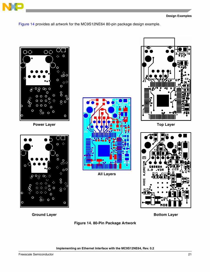
Figure 14 provides all artwork for the MC9S12NE64 80-pin package design example.
Figure 14. 80-Pin Package Artwork
Power Layer
Ground Layer
All Layers
Top Layer
Bottom Layer
Implementing an Ethernet Interface with the MC9S12NE64, Rev. 0.2
Freescale Semiconductor 21
Conclusion
Exposed Flag
Because the 80-pin TQFP-EP package has an exposed flag, which provides additional heat dissipation for the MC9S12NE64, the artwork shows special PCB design to accommodate the exposed flag. There are two ways to accommodate the flag:
• Have a hatched pattern in the solder mask
• Use small copper areas under the flag
The concept is to have about 50% of the flag soldered to the PC board.
Conclusion
The MC9S12NE64 is a highly integrated, flexible and easy-to-use Ethernet-capable microcontroller with an integrated MAC and PHY. No external active components are needed to implement an Ethernet interface. The schematics in this document illustrate the simplicity of implementing such a system.
Interfacing the device to an Ethernet trunk is accomplished with the addition of only four resistors, a decoupling capacitor and an integrated transformer/RJ45 connector. PCB layout around the high-speed LAN magnetics isolation module is critical, as with any high frequency design. Using techniques discussed in this document makes that task easier.
NOTE
With the exception of mask set errata documents, if any other Freescale Semiconductor document contains information that conflicts with the information in the device user guide, the user guide should be considered to have the most current and correct data.
Notes
Implementing an Ethernet Interface with the MC9S12NE64, Rev. 0.2
22 Freescale Semiconductor

Notes
This page is intentionally blank
Implementing an Ethernet Interface with the MC9S12NE64, Rev. 0.2
Freescale Semiconductor 23

AN2759Rev. 0.2, 9/2004
How to Reach Us:
USA/Europe/Locations not listed:Freescale Semiconductor Literature DistributionP.O. Box 5405, Denver, Colorado 802171-800-521-6274 or 480-768-2130
Japan:Freescale Semiconductor Japan Ltd.SPS, Technical Information Center3-20-1, Minami-AzabuMinato-kuTokyo 106-8573, Japan81-3-3440-3569
Asia/Pacific:Freescale Semiconductor H.K. Ltd.2 Dai King StreetTai Po Industrial EstateTai Po, N.T. Hong Kong852-26668334
Learn More:For more information about Freescale Semiconductor products, please visithttp://www.freescale.com
Information in this document is provided solely to enable system and software implementers to use
Freescale Semiconductor products. There are no express or implied copyright licenses granted
hereunder to design or fabricate any integrated circuits or integrated circuits based on the information
in this document.
Freescale Semiconductor reserves the right to make changes without further notice to any products
herein. Freescale Semiconductor makes no warranty, representation or guarantee regarding the
suitability of its products for any particular purpose, nor does Freescale Semiconductor assume any
liability arising out of the application or use of any product or circuit, and specifically disclaims any
and all liability, including without limitation consequential or incidental damages. “Typical” parameters
which may be provided in Freescale Semiconductor data sheets and/or specifications can and do
vary in different applications and actual performance may vary over time. All operating parameters,
including “Typicals” must be validated for each customer application by customer’s technical experts.
Freescale Semiconductor does not convey any license under its patent rights nor the rights of others.
Freescale Semiconductor products are not designed, intended, or authorized for use as components
in systems intended for surgical implant into the body, or other applications intended to support or
sustain life, or for any other application in which the failure of the Freescale Semiconductor product
could create a situation where personal injury or death may occur. Should Buyer purchase or use
Freescale Semiconductor products for any such unintended or unauthorized application, Buyer shall
indemnify and hold Freescale Semiconductor and its officers, employees, subsidiaries, affiliates, and
distributors harmless against all claims, costs, damages, and expenses, and reasonable attorney
fees arising out of, directly or indirectly, any claim of personal injury or death associated with such
unintended or unauthorized use, even if such claim alleges that Freescale Semiconductor was
negligent regarding the design or manufacture of the part.
Freescale™ and the Freescale logo are trademarks of Freescale Semiconductor, Inc. All other product or service names are the property of their respective owners. © Freescale Semiconductor, Inc. 2004.
Recommended