Advanced EDA Tools for Multi-Radio High-Frequency Accurate
IC Design
IEEE Silicon Valley January 28, 2013
Dr. Yasser Hussein [email protected]
CONTENTS
• Introduction
• EDA Evolution
• EDA Comparison
• Design Flow and EDA Integration Overview
• Examples
• Summary & Conclusion

INTRODUCTION
TRENDS • Multiband
› Number of different radios / wireless device is growing.
• Design Cycles › Time allowed for design is shrinking.
• Size › Amount of area for any given function is shrinking.
• Clock Speed › IC operating speed is increasing.
• Application Frequency › New applications are increasing operating frequency.
• Product Lifecycles › Lifetime of any given product is shrinking.
• Internet of Things › Number, standards and types of devices growing rapidly.
3
RF
DES
IGN
CH
ALL
ENG
ES
INTRODUCTION
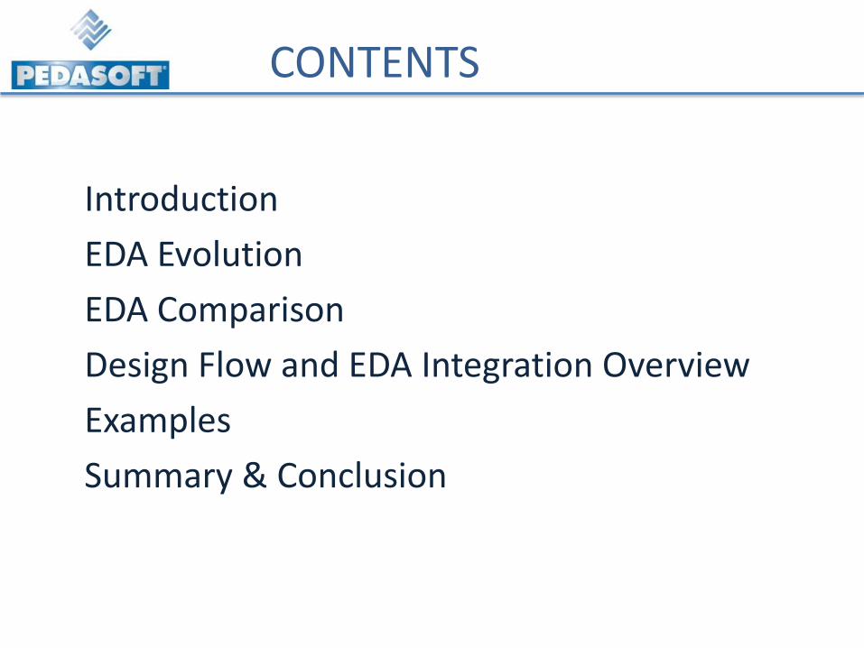
RF DESIGN CHALLENGES • Iterations
› Generally the longest time, not to mention cost, for a single iteration is the prototype fabrication time.
› Reduced number of design iterations is necessary to meet time-to-market expectations.
› Improved simulation accuracy is required in order to reduce the number of iterations, yet the number of design passes to meet the specification has not changed substantially over the last 20 years.
• Tools › Electronic Design Automation (EDA) has roots in two basic approaches:
– Circuit simulators – EM Field solvers
› To overcome the limitations of both, EDA tools have incorporated the ability to paste in blocks of simulation results to permit “co-simulation” of circuit and EM results.
› This approach is limited in its ability to accurately simulate circuit response and hence does not reduce the number of design cycles.
4

INTRODUCTION
RF DESIGN CHALLENGES
5
Transistor
Passives Wire bond

EDA Evolution
EVOLUTION / ACCURACY
6
Circuit simulation
EM-Supreme® HYBRID
Circuit + Blocks
+
EM-CORE® OVERVIEW
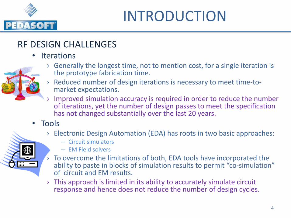
EM SIMULATOR COMPARISON
7
Company P
ed
aSo
ft
Son
net
CST
An
sys
Zela
nd
IMST
Product EM-Core® Sonnet CST-Ems HFSS IE3D Xccel Geometry 2.5 & 3D 2.5D 3D 3D 3D 3D Method FDTD MoM FIM FEM MoM FDTD Time Domain √ X √ X X √ Freq Domain X √ √ √ √ X Accuracy High Medium High High High High Memory Medium Medium High High Medium High Speed Medium Fast Medium Medium Medium Fast Shielded √ √ √ √ √ √ Radiated √ X X √ X X DXF √ √ √ √ √ √ Customizable √ X X X X X Cost Low Medium High High Medium Medium
EM-SUPREME® OVERVIEW
8
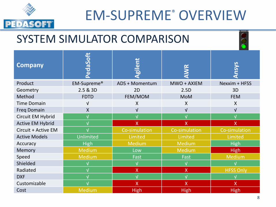
SYSTEM SIMULATOR COMPARISON
Company
Pe
daS
oft
Agi
len
t
AW
R
An
sys
Product EM-Supreme® ADS + Momentum MWO + AXIEM Nexxim + HFSS Geometry 2.5 & 3D 2D 2.5D 3D Method FDTD FEM/MOM MoM FEM Time Domain √ X X X Freq Domain X √ √ √ Circuit EM Hybrid √ √ √ √ Active EM Hybrid √ X X X Circuit + Active EM √ Co-simulation Co-simulation Co-simulation Active Models Unlimited Limited Limited Limited Accuracy High Medium Medium High Memory Medium Low Medium High Speed Medium Fast Fast Medium Shielded √ √ √ √ Radiated √ X X HFSS Only DXF √ √ √ √ Customizable √ X X X Cost Medium High High High
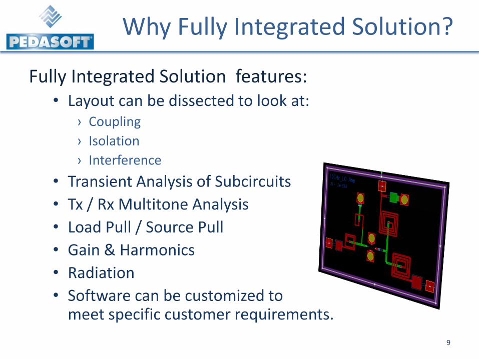
Why Fully Integrated Solution?
Fully Integrated Solution features: • Layout can be dissected to look at:
› Coupling
› Isolation
› Interference
• Transient Analysis of Subcircuits
• Tx / Rx Multitone Analysis
• Load Pull / Source Pull
• Gain & Harmonics
• Radiation
• Software can be customized to meet specific customer requirements.
9
EM-SUPREME® OVERVIEW
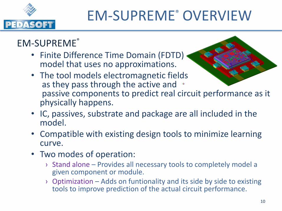
EM-SUPREME®
• Finite Difference Time Domain (FDTD) model that uses no approximations.
• The tool models electromagnetic fields as they pass through the active and passive components to predict real circuit performance as it physically happens.
• IC, passives, substrate and package are all included in the model.
• Compatible with existing design tools to minimize learning curve.
• Two modes of operation: › Stand alone – Provides all necessary tools to completely model a
given component or module. › Optimization – Adds on funtionality and its side by side to existing
tools to improve prediction of the actual circuit performance.
10
CONTENTS
Introduction
EM-Supreme® Overview
Design Flow
• Examples
• Demonstration
• Engagement
• Summary & Conclusion
11

DESIGN FLOW
PORTABILITY
12
Circuit Simulation (i.e. ADS)
Circuit + Layout Simulation (i.e. ADS+ Momentum)
Circuit + Layout + Package Simulation
(i.e. ADS+ Momentum)
Circuit + Layout + Package + PCB Simulation
(i.e. ADS+ Momentum)
EM-Supreme®
Total / Active + Passive /
Simultaneous System Evaluation
HY
BR
ID
HY
BR
ID
HY
BR
ID
EM
COMPLEXITY
DXF / GDS

DESIGN FLOW
13
Design Specification
Schematic Capture
Circuit Simulation
Layout
EM-Core® Simulation
Active Model Insertion
EM-Supreme® Simulation
Parameter Extraction
Parameter Extraction
Actives + Passives
Schematic Conversion
Design Rule Check (DRC)
STAND ALONE MODE
Passives
PedaSoft Solution

DESIGN FLOW
OPTIMIZATION MODE
14
PedaSoft Solution
14
Design Specification
Schematic Capture
Simulation
Layout
Dsgn Rule Check (DRC)
Parameter Extraction
Lay vs Sch Check (LVS)
Final Simulation
Layout Transfer Verification
EM-Core® Simulation
Active Model Insertion
EM-Supreme® Simulation
DXF
GDS
Parameter Extraction
Parameter Extraction
Tape Out
Passives Actives + Passives
Schematic Conversion
DESIGN FLOW
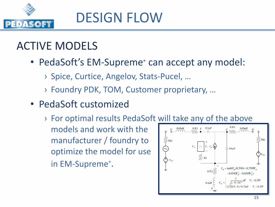
ACTIVE MODELS
• PedaSoft’s EM-Supreme® can accept any model:
› Spice, Curtice, Angelov, Stats-Pucel, …
› Foundry PDK, TOM, Customer proprietary, …
• PedaSoft customized
› For optimal results PedaSoft will take any of the above models and work with the manufacturer / foundry to optimize the model for use
in EM-Supreme®.
15

Things Can Always Go Wrong!
PA Many potential sources of error
› New Dimensions results when EM Simulating the whole structure “i.e. feedback network and vias.
› The feedback line could EM-couple with the substrate, packaging layers, and neighborhood components
› The transistor along with feedback network exist on the top layer of a multilayer substrate with metallization underneath, adding possibilities of coupling that designer needs to account for.
16
W/ Feedback Network
Transistor
W/ VIAs

EXAMPLES
PA DESIGN
2 – 5 GHz flat gain target
17
+ Feedback Network
Transistor
+ VIAs + PCB

EXAMPLES
PA DESIGN (cont.)
18
-25
-20
-15
-10
-5
0
5
0 1 2 3 4 5 6 7 8 9 10 11 12 13 14 15 16 17
Ls=0.1nH
Ls=0.5nH
Ls=1.0nH
S11 (
dB)
-50
-40
-30
-20
-10
0
10
20
30
0 1 2 3 4 5 6 7 8 9 10 11 12 13 14 15 16 17
Ls=0.1nH
Ls=0.5nH
Ls=1.0nH
S21 (
dB)
-25
-20
-15
-10
-5
0
5
0 1 2 3 4 5 6 7 8 9 10 11 12 13 14 15 16 17
Cgs0=3pF
Cgs0=6pF
Cgs0=9pF
S11 (
dB)
-50
-40
-30
-20
-10
0
10
20
30
0 1 2 3 4 5 6 7 8 9 10 11 12 13 14 15 16 17
Cgs0=3pF
Cgs0=6pF
Cgs0=9pF
S21 (
dB)

EXAMPLES
PA DESIGN (cont.)
19
-40
-35
-30
-25
-20
-15
-10
-5
0
5
0 1 2 3 4 5 6 7 8 9 10 11 12 13 14 15 16 17
A1=0.2595
A1=0.3595
A1=0.4595
S1
1 (
dB
)
-50
-40
-30
-20
-10
0
10
20
30
0 1 2 3 4 5 6 7 8 9 10 11 12 13 14 15 16 17
A1=0.2595
A1=0.3595
A1=0.4595
S2
1 (
dB
)

EXAMPLES
PA DESIGN (cont.)
20
-25
-20
-15
-10
-5
0
5
10
15
20
2 3 4 5 6 7 8 9 10
S2
1(d
B)
Frequency (GHz)
-18
-16
-14
-12
-10
-8
-6
-4
-2
0
2 3 4 5 6 7 8 9 10
S1
1 (
dB
)
Frequency (GHz)

EXAMPLES
PA DESIGN (cont.)
• Comparison of same circuit using co-simulation
21
-25
-20
-15
-10
-5
0
5
10
15
20
2 3 4 5 6 7 8 9 10
S2
1(d
B)
Frequency (GHz)
-18
-16
-14
-12
-10
-8
-6
-4
-2
0
2 3 4 5 6 7 8 9 10
S1
1 (
dB
)
Frequency (GHz)
EXAMPLES
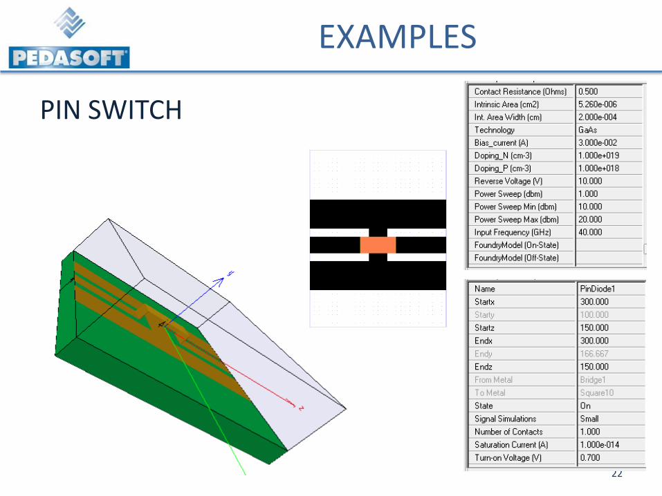
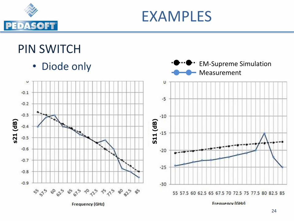
PIN SWITCH
22
EXAMPLES
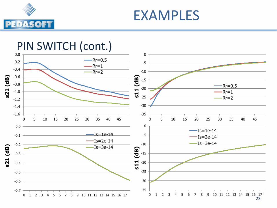
PIN SWITCH (cont.)
23
-1.6
-1.4
-1.2
-1.0
-0.8
-0.6
-0.4
-0.2
0.0
0 5 10 15 20 25 30 35 40 45
Rr=0.5
Rr=1
Rr=2
-35
-30
-25
-20
-15
-10
-5
0
0 5 10 15 20 25 30 35 40 45
Rr=0.5
Rr=1
Rr=2 s2
1 (
dB
)
s1
1 (
dB
)
-0.7
-0.6
-0.5
-0.4
-0.3
-0.2
-0.1
0.0
0 1 2 3 4 5 6 7 8 9 10 11 12 13 14 15 16 17
Is=1e-14
Is=2e-14
Is=3e-14
-35
-30
-25
-20
-15
-10
-5
0
0 1 2 3 4 5 6 7 8 9 10 11 12 13 14 15 16 17
Is=1e-14
Is=2e-14
Is=3e-14
s2
1 (
dB
)
s1
1 (
dB
)
EXAMPLES
PIN SWITCH
• Diode only
24
EM-Supreme Simulation Measurement
S1
1 (
dB
)
s2
1 (
dB
)
EXAMPLES
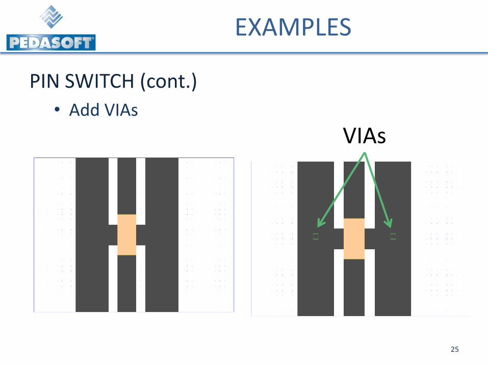
PIN SWITCH (cont.)
• Add VIAs
25
VIAs

EXAMPLES
PIN SWITCH (cont.)
26
s21 s11
W/O VIAS
W/ VIAS
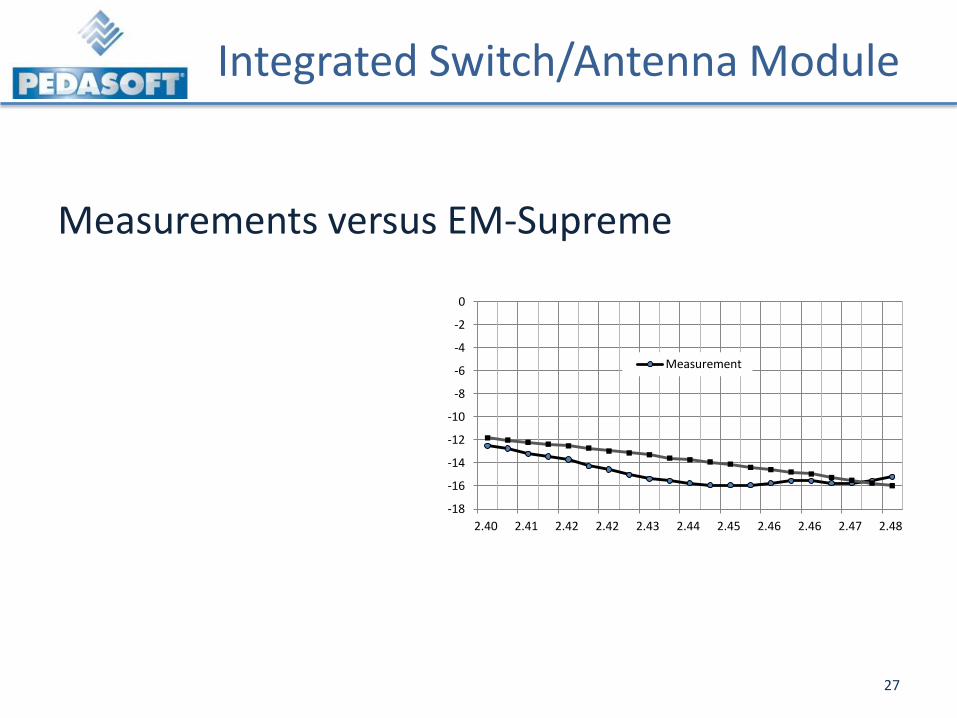
Integrated Switch/Antenna Module
Measurements versus EM-Supreme
27
-18
-16
-14
-12
-10
-8
-6
-4
-2
0
2.40 2.41 2.42 2.42 2.43 2.44 2.45 2.46 2.46 2.47 2.48
Measurement

Integrated Switch/Antenna Module
Measurement versus EM-Supreme
28
0 10
20 30
40
50
60
70
80
90
100
110
120
130
140 150
160 170
180 190
200 210
220
230
240
250
260
270
280
290
300
310
320 330
340 350
-15
-10
-5
0
5
Measurement
-10
-5
0
5 0
10 20 30
40
50
60
70
80
90
100
110
120
130
140 150
160 170 180
190 200 210
220
230
240
250
260
270
280
290
300
310
320 330
340 350 Measure…
Radiated Emissions
E-Field
H-Field
Two EVB Xmission Line Lengths
SUMMARY & CONCLUSION
EM-Supreme includes electromagnetics to model field distributed-effects, coupling, radiation, as well as parasitic effects at RF and millimeter-wave bands; for active, passive, and complete RF modules.
Technology supported includes, but not limited to,: PHEMTS, Silicon Germanium, Gallium Arsenide, Aluminium Gallium Arsenide, Indium Gallium Phosphide HBT’s and PIN diodes. With the method, RF designer can model CMOS as well as Gallium Arsenide and Gallium Nitride FETs.
EM-Supreme eliminates excessive design cycles (typically 3 to 4) and/or inefficient designs which would translate into high costs and ultimately lost time-to-market opportunities.
29
EM-Supreme is the first EM simulator for the whole chip “transistors plus passives” to including all parasitic effects, radiation coupling and inference in a single software tool.
The tool is fully customized. The tool comes as a stripped or customized version based on special foundry or active models “i.e. cost effective and flexible“
Easy to Use “just import the layout in DXF and then insert active components”
We have a very well established team "programmers, GUI's, RF engineers, and packaging designers”
The current version is very stable version that has been used by dozens of RF engineering teams
Windows compatible “can run efficiently on any windows operating system including windows 7.0”
SUMMARY & CONCLUSION
30

Thanks You
More info. can be found at www.pedasoft.com
or email me at
31
Recommended