Active Filter for Single-Phase Power System
A Major Qualifying Project Report submitted to the Faculty of Worcester
Polytechnic Institute in Partial Fulfillment of the Requirements for the
Degree of the Bachelor of Science
By:
____________________________
Brent McGrath
____________________________
Wesley DeChristofaro
____________________________
Thomas Powell
Submitted On: May 1, 2014
Submitted To:
_______________________________________________________________
Professor Alexander Emanuel, Advisor, Electrical and Computer Engineering

i
Abstract
This study investigates the application and functionality of pure active power filters for current
compensation in single-phase power systems. A small scale proof of concept design was
constructed, using components which were studied, justified, and chosen based upon desired
characteristics. The components were simulated on several different platforms to analyze their
potential design feasibility. Based upon the study and simulation of this system the pure active
power filter can be confirmed as a reputable form of harmonic filtering for single-phase power
systems.

ii
Acknowledgements
Throughout the undertaking of this project, there have been several people who have proven to be
great resources. First, Professor Emanuel, whose overall knowledge of the power realm and step-
by-step guidance helped in realizing the important aspects of the project. Next, Radu David,
whose background in DSP and experience with dsPIC microprocessing chips were vital in helping
the group to understand the thought process behind selecting, using, and coding a dsPIC chip for a
real-time DSP application. The team would also like to thank Robert Boise for his assistance
during the acquisition of various design components. A final thank you goes out to the other
fellow students who have helped provide assistance along the way, without all of you this project
would not have been possible.

iii
Authorship
Abstract
Written By
o Wesley DeChristofaro, Brent McGrath
Chapter One - Introduction
Written By
o Wesley DeChristofaro
Chapter Two – Background
Written By
o Wesley DeChristofaro, Brent McGrath, Thomas Powell
Chapter Three – System Requirements
Written By
o Brent McGrath
Chapter Four – Overall Design
Written By
o Wesley DeChristofaro(4.2), Brent McGrath(4.1,4.3-6)
Chapter Five – System Requirements
Written By
o Brent McGrath
Chapter Six – Digital Control System
Written By
o Brent McGrath(6-6.6.1), Thomas Powell(6.2)
Chapter Seven – Simulations
Written By
o Wesley DeChristofaro(7.2-3), Brent McGrath(7.1)
Chapter Eight – Future Implementation Considerations
Written By
o Brent McGrath
Chapter Nine – References
Written By
o Brent McGrath

iv
Table of Contents Abstract ............................................................................................................................................... i
Acknowledgements ............................................................................................................................ ii
Authorship......................................................................................................................................... iii
1. Introduction ................................................................................................................................ 1
2. Background ................................................................................................................................. 2
3. System Requirements ............................................................................................................... 13
4. Overall Design .......................................................................................................................... 15
4.1 Non-linear Load ..................................................................................................................... 16
4.2 Active Power Filter ................................................................................................................ 16
4.3 Sliding Window Fast Fourier Transform ............................................................................... 17
4.4 Ideal Current & Harmonic Distortion Calculations ............................................................... 18
4.5 Duty Cycle Algorithm & PWM Generation .......................................................................... 18
4.6 MOSFET Gate Driver ............................................................................................................ 18
5. System Specifications ............................................................................................................... 19
5.1 MOSFET’s ............................................................................................................................. 19
5.2 Digital Microcontroller .......................................................................................................... 21
5.3 MOSFET Gate Driver ............................................................................................................ 25
6. Digital Control System Implementation ................................................................................... 25
6.1 Main Clock & Auxiliary Clock Configuration ...................................................................... 25
6.2 ADC Configuration ................................................................................................................ 26
6.3 Timer1 Configuration – ADC interrupts ................................................................................ 27
6.4 Sliding Window FFT .............................................................................................................. 28
6.5 Duty Cycle Algorithm & PWM Generation .......................................................................... 33
6.6 Alternative Applications ........................................................................................................ 36
6.6.1 PWM Configuration ........................................................................................................ 37
7. Simulations ............................................................................................................................... 40
7.1 Digital Control Algorithm Simulation ................................................................................... 40
7.2 PSPICE Simulations ............................................................................................................... 43
7.2.1 Quarter Bridge ................................................................................................................. 44

v
7.2.2 Half Bridge ...................................................................................................................... 44
7.2.3 The PSPICE Switch ......................................................................................................... 45
7.2.4 Test Circuit 1 ................................................................................................................... 47
7.2.5 Test Circuit 2 ................................................................................................................... 47
7.2.6 Test Circuit 3 ................................................................................................................... 48
7.2.7 Test Circuit 4 ................................................................................................................... 48
7.2.8 Test Circuit 5 ................................................................................................................... 49
7.2.9 Test Circuit 6 ................................................................................................................... 50
7.2.10 Test Circuit 7 ................................................................................................................. 50
7.2.11 Test Circuit 8 ................................................................................................................. 51
7.2.12 Test Circuit 9 ................................................................................................................. 52
7.3 PSIM Simulations .................................................................................................................. 52
7.3.1 PWM Creation ................................................................................................................. 54
7.3.2 PWM Current Adaptation ................................................................................................ 56
7.3.3 System Imperfections ...................................................................................................... 58
7.3.4 Attaching the Non-Linear Load ....................................................................................... 59
7.3.5 Successfully Attaching the Non-Linear Load ................................................................. 60
7.3.6 Issues with PSIM Simulations ......................................................................................... 62
7.3.7 Summarized Functionality and Results ........................................................................... 62
7.3.8 Additional PSIM Ideas .................................................................................................... 63
8. Future Implementation Considerations .................................................................................... 64
8.1 Selection of MCU – Resource Management .......................................................................... 64
8.2 Complex Duty Cycle Algorithms ........................................................................................... 65
Appendices ....................................................................................................................................... 66
Appendix A: Constants_Globals_Prototypes.h Header File ........................................................ 66
Appendix B: Init_Functions(GS502).h Header File .................................................................... 68
Appendix C: MQP_Code.c Source Code File .............................................................................. 73
Appendix D: Enum_States.h Header File .................................................................................... 78
Appendix E: Digital Control Simulation Matlab Code ................................................................ 79
References ........................................................................................................................................ 82
1
1. Introduction
Within the world of electrical engineering where silicon chips hold trillions of transistors and
billions of people depend on the function of computers there are countless ways that the basic
principles of electricity have been applied to human life. Deep within that realm of engineering
lives the study of energy transfer, transduction, transmission, and perhaps most importantly –
control. Electricity provided to the masses in a common 50 hertz or 60 hertz waveform at some
voltage is certainly a blessing to the world of electronics, but not all devices can work with such an
input. When there is some device or application that desires a lower/higher voltage, current,
frequency, or even a DC characteristic there has to be a change within that device rather than the
entire utility grid. This is, in short, part of the job of power electronics. Power electronics includes
anything that works to change or control a certain input to attain some different output for the use
of a device.[1]
When working within large or small scale power systems however the control of electricity and
power flow is no simple feat. Resistors are linear and easy to work with, but most devices contain
more complicated non-linear, non-ideal components that by themselves can be difficult to control.
Worse still however, are the underlying effects of non-linear components such as diode bridges
that can create what are called harmonics. These harmonics exist at frequencies at multiplies of the
fundamental or desired frequency with decreasing magnitude as they increase in order. This
means that these additional harmonics are added to the original waveform and create some form of
undesired distortion. The last harmonic which has a noticeable impact on the original waveform
would be the 19th
harmonic.[2]
In the world of macro power, where the utility has many homes, schools, hospitals, police stations,
libraries, and other large buildings to supply it clearly has many connections. All of these buildings
are considered non-linear, non-ideal loads which mean they will create harmonics. These
harmonics, due to the loads, will feed into the line current and may be “passed down the chain”
increasing the distortion. Power electronics involves the study of various ways of rectifying this
situation.
Usually it is the responsibility of the consumer, based upon IEEE standard 519, to monitor and
reduce the harmonic production of some loads. That production is greater for some than others, but
with the correct knowledge it can be filtered. The filtering process depends on the application, but
a popular form of filtering is utilizing active filters instead of passive filters to adjust to the
changing harmonics to keep consistent filtering. This is important because each time a new
consumer is added the harmonics on the line can change and affect what would need to be filtered
somewhere else. Passive filters are set to filter a certain type and frequency of waveform (to a
certain order of harmonic), while active filters can be made to adapt.[3]
These active filters work based off of a thorough understanding of the frequency and time domains
and their relations. This is important since most things that consumers are concerned with can be
explained simply in the time domain, while the more intensive concerns of the utility and providers
are best handed in the frequency domain. This is because, as previously stated, the harmonic
2
distortion can be seen on the load lines, but are added to the fundamental. The ability to separate
the harmonics from the fundamental exists much more appropriately in the frequency domain than
in the time domain since harmonics occur at the same time but different frequencies than the
fundamental or desired waveform.
In this report the study of a pure active filter, one without passive components, is centered around
the idea that one can filter out harmonics of a non-linear load by understanding the difference
between the line current (including harmonics) and what the ideal current would be. If this is the
case then an active filter that responds to any change in the line current should be able to filter any
change and always result in a clean, clear output waveform.
2. Background
A filter in the most common sense is something that removes an unwanted feature, or aspect of
something. This can range from filtering water to filtering your search for MQP parts on any given
cite. In signal processing and engineering the only difference is that the unwanted component may
be voltage or current distortion. Take for example the low and high pass filters found in basic
electrical engineering and E&M theory, as shown in Figure 2.1, these filters can each be used to
limit the operating frequencies of a circuit.
Figure 2.1: Passive Low and High Pass Filters
These filters pass low or high frequencies regardless of whether it is a fundamental or a 13th
harmonic. This means that these filters, known to be part of the class of passive filters, can be used
to filter out higher order frequencies. These filters have an element known as a time constant
which is often equal to the resistance multiplied by the capacitance of the “RC” connection. This
time constant is called τ. The cutoff frequencies of the filters are directly dependent on this
constant. A simple equation to represent the cutoff frequencies for both the basic high and low pass
RC filters is shown in Equation 2.1.
(2.1)
3
It should be noted that there are other kinds of low and high pass filters, such as second and third
order filters, but these are the simplest ones.
Additionally low and high pass filters exist in the active realm of electrical engineering. Although
not referring to the class of active filters that this project pursues. These alternative filters use an
operational amplifier in the configurations shown in Figure 2.2 to limit the bandwidth of Op-Amp
based filters. The difference between these active filters and the active filter described throughout
this report exists in how they are maintained. The filters that this project concerns are based around
varying types of bridges and how the transistors in these bridges are driven to compensate for
current.
Figure 2.2: Active Low and Active High Pass Filters
Passive filters, as those shown in Figure 2.1, include any filter that is constructed out of passive
components such as inductors, capacitors and resistors. Although these components can at times be
quite complex the passive term they earned is not to imply less functionality. They are called
passive filters because their bandwidth and use is decided before construction and does not change
without physical changing the circuit in which they exist. In other words a passive filter can be
created to work with a certain set of frequencies and loads and then forgotten. Passive filters work
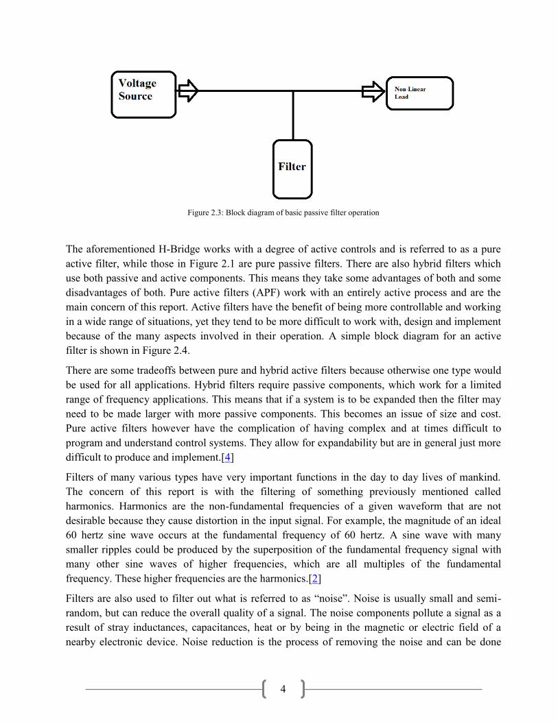
very well with linear loads. The basic block diagram for such a filter is shown in Figure 2.3. An
active filter on the other hand works with some kind of control scheme to allow it to constantly
change to its load within certain restrictions. A common type of active filter is one made from an
H-bridge of some type of transistor, whether it is a MOSFET, IGBT or BJT. This type of filter
operates through the driving of the transistors to create some type of “filtering” or “compensation”
current that would cancel out distortion.
4
Figure 2.3: Block diagram of basic passive filter operation
The aforementioned H-Bridge works with a degree of active controls and is referred to as a pure
active filter, while those in Figure 2.1 are pure passive filters. There are also hybrid filters which
use both passive and active components. This means they take some advantages of both and some
disadvantages of both. Pure active filters (APF) work with an entirely active process and are the
main concern of this report. Active filters have the benefit of being more controllable and working
in a wide range of situations, yet they tend to be more difficult to work with, design and implement
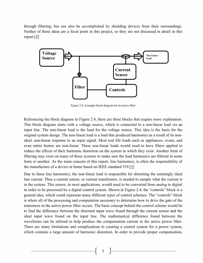
because of the many aspects involved in their operation. A simple block diagram for an active
filter is shown in Figure 2.4.
There are some tradeoffs between pure and hybrid active filters because otherwise one type would
be used for all applications. Hybrid filters require passive components, which work for a limited
range of frequency applications. This means that if a system is to be expanded then the filter may
need to be made larger with more passive components. This becomes an issue of size and cost.
Pure active filters however have the complication of having complex and at times difficult to
program and understand control systems. They allow for expandability but are in general just more
difficult to produce and implement.[4]
Filters of many various types have very important functions in the day to day lives of mankind.
The concern of this report is with the filtering of something previously mentioned called
harmonics. Harmonics are the non-fundamental frequencies of a given waveform that are not
desirable because they cause distortion in the input signal. For example, the magnitude of an ideal
60 hertz sine wave occurs at the fundamental frequency of 60 hertz. A sine wave with many
smaller ripples could be produced by the superposition of the fundamental frequency signal with
many other sine waves of higher frequencies, which are all multiples of the fundamental
frequency. These higher frequencies are the harmonics.[2]
Filters are also used to filter out what is referred to as “noise”. Noise is usually small and semi-
random, but can reduce the overall quality of a signal. The noise components pollute a signal as a
result of stray inductances, capacitances, heat or by being in the magnetic or electric field of a
nearby electronic device. Noise reduction is the process of removing the noise and can be done
5
through filtering, but can also be accomplished by shielding devices from their surroundings.
Neither of these ideas are a focal point in this project, so they are not discussed in detail in this
report.[5]
Figure 2.4: Example block diagram for an active filter
Referencing the block diagram in Figure 2.4, there are three blocks that require more explanation.
This block diagram starts with a voltage source, which is connected to a non-linear load via an
input line. The non-linear load is the load for the voltage source. This idea is the basis for the
original system design. The non-linear load is a load that produced harmonics as a result of its non-
ideal, non-linear response to an input signal. Most real life loads such as appliances, ovens, and
even entire homes are non-linear. These non-linear loads would need to have filters applied to
reduce the effects of their harmonic distortion on the system in which they exist. Another form of
filtering may exist on many of these systems to make sure the load harmonics are filtered in some
form or another. As the main concern of this report, line harmonics, is often the responsibility of
the manufacture of a device or home based on IEEE standard 519.[3]
Due to these line harmonics, the non-linear load is responsible for distorting the seemingly ideal
line current. Thus a current sensor, or current transformer, is needed to sample what the current is
in the system. This sensor, in most applications, would need to be converted from analog to digital
in order to be processed by a digital control system. Shown in Figure 2.4, the “controls” block is a
general idea, which could represent many different types of control schemes. The “controls” block
is where all of the processing and computation necessary to determine how to drive the gate of the
transistors in the active power filter occurs. The basic concept behind the control scheme would be
to find the difference between the distorted input wave found through the current sensor and the
ideal input wave found on the input line. The mathematical difference found between the
waveforms can be utilized to help produce the compensation current in the active power filter.
There are many limitations and complications in creating a control system for a power system,
which contains a large amount of harmonic distortion. In order to provide proper compensation,
6
ideas such as the Phase-locked Loop(PLL) and/or power factor correction(PFC) can be
implemented as components in the control system.
The method used to implement the control system depends on whether it resides in the digital or
analog domain. In short, analog is things such as audio whether it be generated or the human voice.
Digital on the other hand is usually things represented with “1” or “0” or “yes” or “no.” The
Digital domain seems like the best option for the control scheme because the time editing the code
should be less than the time necessary to acquire additional analog components for an analog
control scheme. An analog design might also require the rewiring of components and more time
spent in circuit debugging.
Due to the selection of the digital control for the design, a method of converting the analog signal
to the digital domain was necessary. The analog-to-digital converter(ADC) was selected as the
component which would take care of that task. The ADC is used to convert analog signals into
digital signals. The ADC is an important component in digital devices, such as computers, because
these devices cannot process continuous time analog signals. All digital devices operate in the
discrete domain, so analog signals need to be sampled and converted into a binary representation
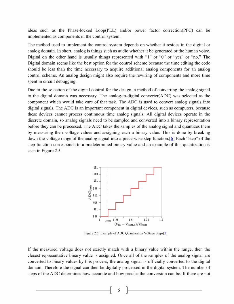
before they can be processed. The ADC takes the samples of the analog signal and quantizes them
by measuring their voltage values and assigning each a binary value. This is done by breaking
down the voltage range of the analog signal into a piece-wise step function.[6] Each “step” of the
step function corresponds to a predetermined binary value and an example of this quantization is
seen in Figure 2.5.
Figure 2.5: Example of ADC Quantization Voltage Steps[7]
If the measured voltage does not exactly match with a binary value within the range, then the
closest representative binary value is assigned. Once all of the samples of the analog signal are
converted to binary values by this process, the analog signal is officially converted to the digital
domain. Therefore the signal can then be digitally processed in the digital system. The number of
steps of the ADC determines how accurate and how precise the conversion can be. If there are not
7
enough steps present then inaccuracies and loss of data can be introduced because the changes are
too large. The analog signal would not be accurately represented in the digital domain when
converted to binary.
The digital control requires a method of determining the fundamental frequency of the input
current signal. A possible method is using either a Discrete Fourier Transform(DFT) or a Fast
Fourier Transform(FFT). The DFT and FFT are both mathematical algorithms, which take a signal
from the time domain and convert it into the frequency domain. The DFT and FFT both produce
the same result, but the FFT algorithm is much faster. The algorithms allow for a time signal to be
viewed in the frequency domain, where the magnitudes of the different frequency components in
the input signal can be observed. The frequency with the largest magnitude is the fundamental
frequency and other frequency components of lower magnitude could be caused by noise,
interference, or other harmonic frequency content. By selecting the frequency bin with the highest
magnitude, the fundamental frequency can easily be extracted.
The FFT is labeled with the word, “Fast,” because the FFT algorithm dramatically cuts down on
the number of calculations which occur compared to the DFT. The formula for the DFT is shown
in Equation 2.2.
( ) ∑ [ ]
( )
For each new data point k, N multiplications and N-1 additions are completed. This results in
roughly N2 computations after completing the direct Discrete Fourier Transform. By using the Fast
Fourier Transform you can perform the same operation in N*log2*N computations. The difference
in the number of total computations may not seem dramatic, but if a large number of samples are
being iterated over, the difference can be significant. For example, if you have a set of data with
N= 10^8 samples, then a direct Discrete Fourier Transform would take 10^
16 calculations, but if
you use the Fast Fourier Transform then it would only take 26.5x10^8 calculations. If each
calculation took 1 nanosecond then the Fast Fourier Transform would take 2.65 seconds, while the
direct Discrete Fourier Transform would take over 115 days! Based on this data, if a large number
of samples are being iterated over, the Fast Fourier Transform is the only algorithm which
completes in a reasonable amount of time. For this application, the Fast Fourier Transform is
essential to achieving a real-time system.
The objective behind the Fast Fourier Transform is divide-and-conquer. The first step in the FFT
process is to take the data collected via the ADC and to break it down into parts. This division is
done so that each part can be repeated to form a periodic signal of its own. Each of these periodic
signals is then passed through its own Discrete Fourier Transform. This results in each signal
having its own magnitude results for particular frequencies. The results from each signal are then
added together, which results in a complete Discrete Fourier Transform of the input signal, but at a
much greater speed then if the entire signal was processed at once. For example, take Figure 2.6,
which is a complex signal.[8]

8
Figure 2.6: Example of a Complex Signal[8]
If the complex signal is broken down into smaller parts, each of the smaller parts can be copied
and extended to form periodic sequences. This method allows the Discrete Fourier Transform
algorithm to become more manageable. An example of a smaller section of the signal found in
Figure 2.6 can be seen in Figure 2.7.
Figure 2.7: A smaller section of the signal of Figure 2.6[8]
If the smaller section seen in Figure 2.7 was extended to become periodic, the signal would look
like the signal seen in Figure 2.8. This signal can be passed through the Discrete Fourier
Transform.[8]
Time (s)
Time (s)
Amplitude (V)
Amplitude (V)
9
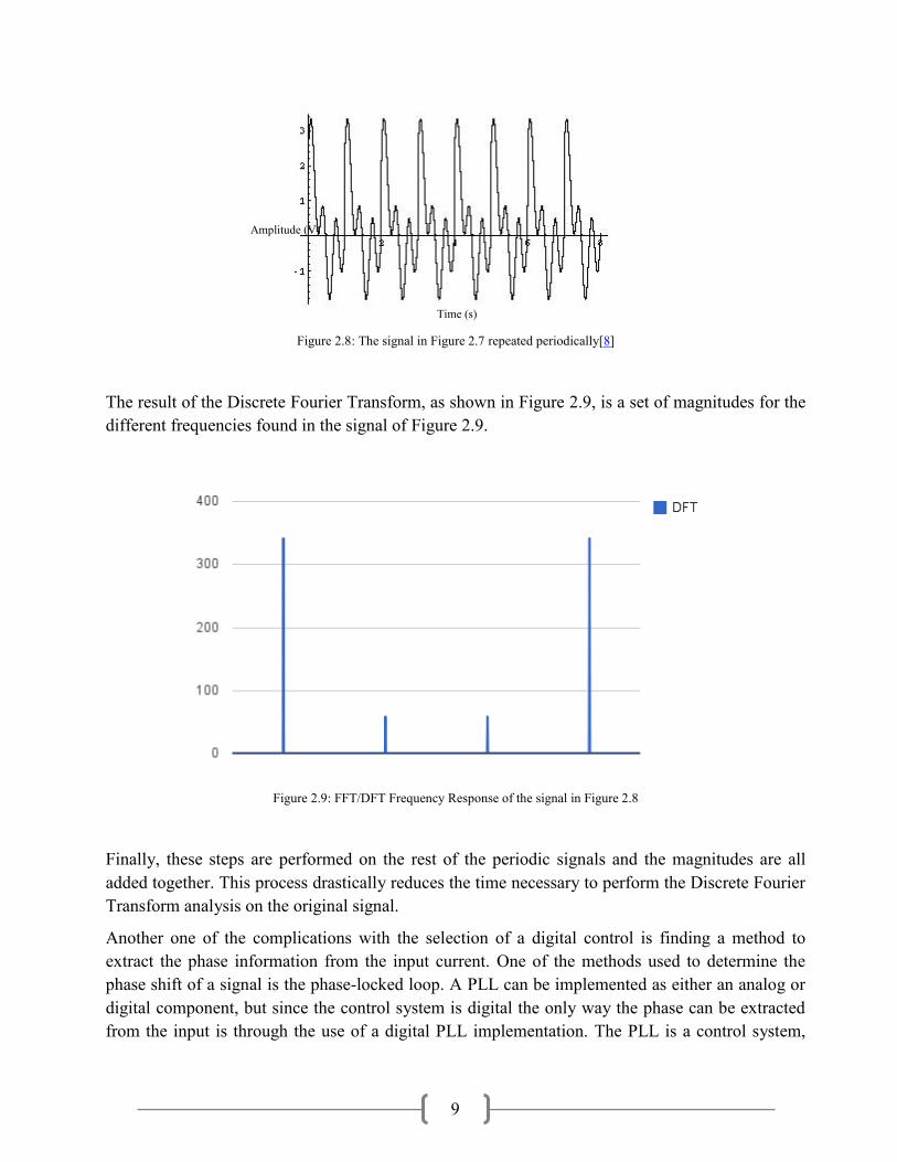
Figure 2.8: The signal in Figure 2.7 repeated periodically[8]
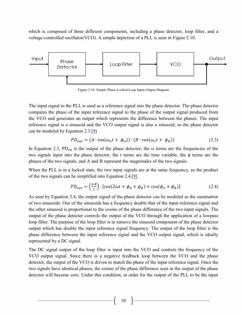
The result of the Discrete Fourier Transform, as shown in Figure 2.9, is a set of magnitudes for the
different frequencies found in the signal of Figure 2.9.
Figure 2.9: FFT/DFT Frequency Response of the signal in Figure 2.8
Finally, these steps are performed on the rest of the periodic signals and the magnitudes are all
added together. This process drastically reduces the time necessary to perform the Discrete Fourier
Transform analysis on the original signal.
Another one of the complications with the selection of a digital control is finding a method to
extract the phase information from the input current. One of the methods used to determine the
phase shift of a signal is the phase-locked loop. A PLL can be implemented as either an analog or
digital component, but since the control system is digital the only way the phase can be extracted
from the input is through the use of a digital PLL implementation. The PLL is a control system,
Time (s)
Amplitude (V)
10
which is composed of three different components, including a phase detector, loop filter, and a
voltage-controlled oscillator(VCO). A simple depiction of a PLL is seen in Figure 2.10.
Figure 2.10: Simple Phase-Locked Loop Input-Output Diagram
The input signal to the PLL is used as a reference signal into the phase detector. The phase detector
compares the phase of the input reference signal to the phase of the output signal produced from
the VCO and generates an output which represents the difference between the phases. The input
reference signal is a sinusoid and the VCO output signal is also a sinusoid, so the phase detector
can be modeled by Equation 2.3.[9]
( ( )) ( ( )) (2.3)
In Equation 2.3, PDout is the output of the phase detector, the ω terms are the frequencies of the
two signals input into the phase detector, the t terms are the time variable, the ϕ terms are the
phases of the two signals, and A and B represent the magnitudes of the two signals.
When the PLL is in a locked state, the two input signals are at the same frequency, so the product
of the two signals can be simplified into Equation 2.4.[9]
(
) [ ( ) ( )] (2.4)
As seen by Equation 2.4, the output signal of the phase detector can be modeled as the summation
of two sinusoids. One of the sinusoids has a frequency double that of the input reference signal and
the other sinusoid is proportional to the cosine of the phase difference of the two input signals. The
output of the phase detector controls the output of the VCO through the application of a lowpass
loop filter. The purpose of the loop filter is to remove the sinusoid component of the phase detector
output which has double the input reference signal frequency. The output of the loop filter is the
phase difference between the input reference signal and the VCO output signal, which is ideally
represented by a DC signal.
The DC signal output of the loop filter is input into the VCO and controls the frequency of the
VCO output signal. Since there is a negative feedback loop between the VCO and the phase
detector, the output of the VCO is driven to match the phase of the input reference signal. Once the
two signals have identical phases, the cosine of the phase difference seen in the output of the phase
detector will become zero. Under this condition, in order for the output of the PLL to be the input
11
frequency, the nominal frequency of the VCO needs to be set to the ideal input frequency
beforehand.[9]
Since in the project a digital control is paired with an analog system, there needs to be a way for
the two subsystems to communicate with one another. The purpose of the digital control is to drive
the gates of the transistors in the active power filter, so a possible method would be pulse-width
modulation(PWM). The PWM waveform applied to the active power filter does not produce a
predetermined analog signal; it produces a signal that will dynamically control the on time of the
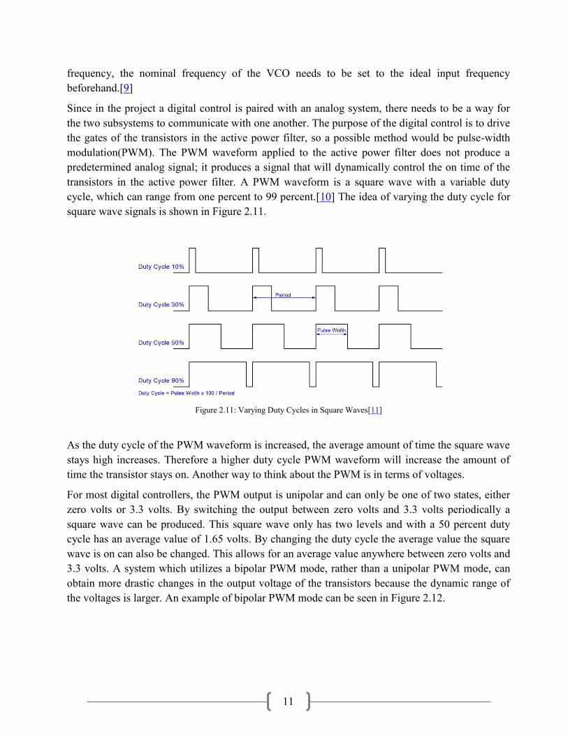
transistors in the active power filter. A PWM waveform is a square wave with a variable duty
cycle, which can range from one percent to 99 percent.[10] The idea of varying the duty cycle for
square wave signals is shown in Figure 2.11.
Figure 2.11: Varying Duty Cycles in Square Waves[11]
As the duty cycle of the PWM waveform is increased, the average amount of time the square wave
stays high increases. Therefore a higher duty cycle PWM waveform will increase the amount of
time the transistor stays on. Another way to think about the PWM is in terms of voltages.
For most digital controllers, the PWM output is unipolar and can only be one of two states, either
zero volts or 3.3 volts. By switching the output between zero volts and 3.3 volts periodically a
square wave can be produced. This square wave only has two levels and with a 50 percent duty
cycle has an average value of 1.65 volts. By changing the duty cycle the average value the square
wave is on can also be changed. This allows for an average value anywhere between zero volts and
3.3 volts. A system which utilizes a bipolar PWM mode, rather than a unipolar PWM mode, can
obtain more drastic changes in the output voltage of the transistors because the dynamic range of
the voltages is larger. An example of bipolar PWM mode can be seen in Figure 2.12.
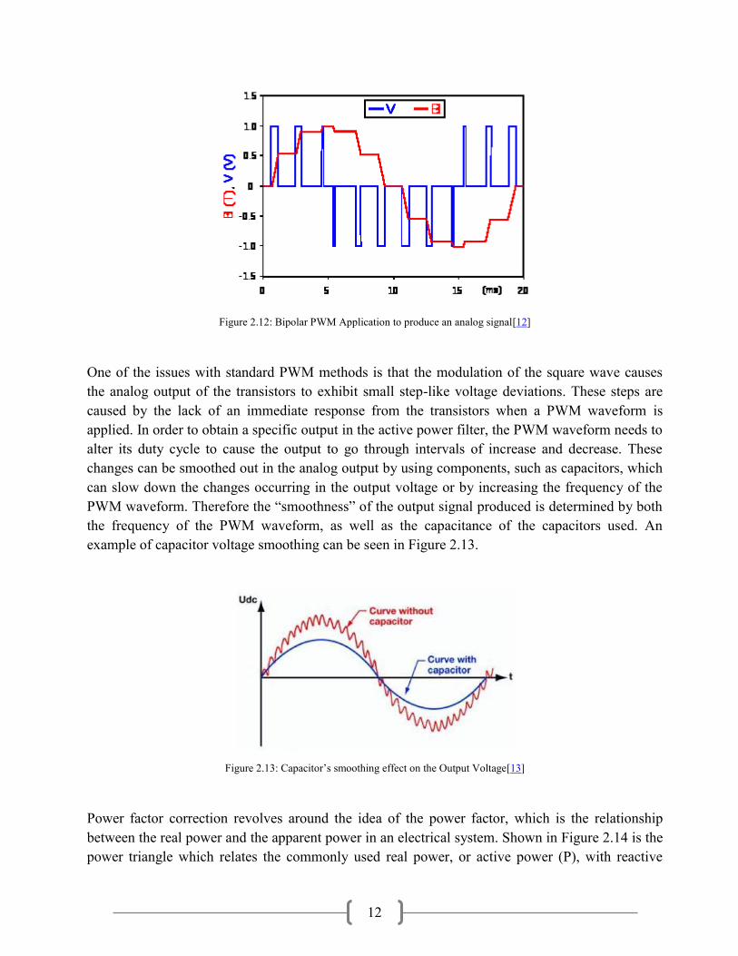
12
Figure 2.12: Bipolar PWM Application to produce an analog signal[12]
One of the issues with standard PWM methods is that the modulation of the square wave causes
the analog output of the transistors to exhibit small step-like voltage deviations. These steps are
caused by the lack of an immediate response from the transistors when a PWM waveform is
applied. In order to obtain a specific output in the active power filter, the PWM waveform needs to
alter its duty cycle to cause the output to go through intervals of increase and decrease. These
changes can be smoothed out in the analog output by using components, such as capacitors, which
can slow down the changes occurring in the output voltage or by increasing the frequency of the
PWM waveform. Therefore the “smoothness” of the output signal produced is determined by both
the frequency of the PWM waveform, as well as the capacitance of the capacitors used. An
example of capacitor voltage smoothing can be seen in Figure 2.13.
Figure 2.13: Capacitor’s smoothing effect on the Output Voltage[13]
Power factor correction revolves around the idea of the power factor, which is the relationship
between the real power and the apparent power in an electrical system. Shown in Figure 2.14 is the
power triangle which relates the commonly used real power, or active power (P), with reactive
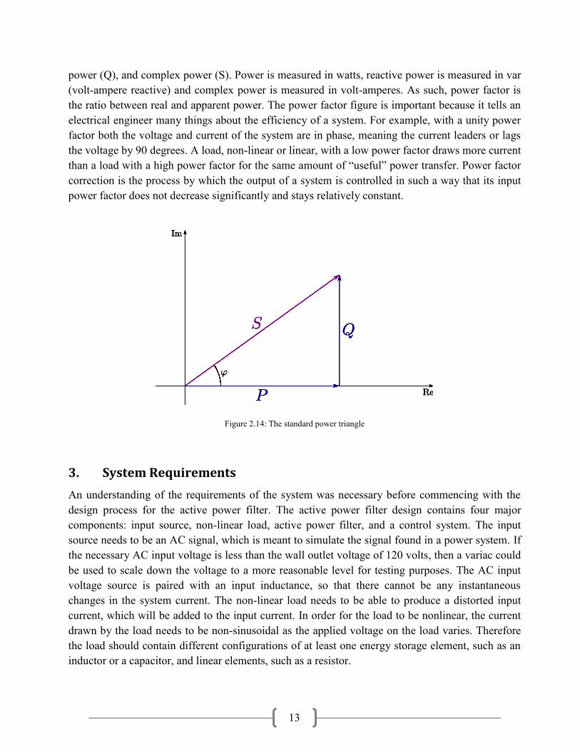
13
power (Q), and complex power (S). Power is measured in watts, reactive power is measured in var
(volt-ampere reactive) and complex power is measured in volt-amperes. As such, power factor is
the ratio between real and apparent power. The power factor figure is important because it tells an
electrical engineer many things about the efficiency of a system. For example, with a unity power
factor both the voltage and current of the system are in phase, meaning the current leaders or lags
the voltage by 90 degrees. A load, non-linear or linear, with a low power factor draws more current
than a load with a high power factor for the same amount of “useful” power transfer. Power factor
correction is the process by which the output of a system is controlled in such a way that its input
power factor does not decrease significantly and stays relatively constant.
Figure 2.14: The standard power triangle
3. System Requirements
An understanding of the requirements of the system was necessary before commencing with the
design process for the active power filter. The active power filter design contains four major
components: input source, non-linear load, active power filter, and a control system. The input
source needs to be an AC signal, which is meant to simulate the signal found in a power system. If
the necessary AC input voltage is less than the wall outlet voltage of 120 volts, then a variac could
be used to scale down the voltage to a more reasonable level for testing purposes. The AC input
voltage source is paired with an input inductance, so that there cannot be any instantaneous
changes in the system current. The non-linear load needs to be able to produce a distorted input
current, which will be added to the input current. In order for the load to be nonlinear, the current
drawn by the load needs to be non-sinusoidal as the applied voltage on the load varies. Therefore
the load should contain different configurations of at least one energy storage element, such as an
inductor or a capacitor, and linear elements, such as a resistor.

14
The active power filter has a couple possible design options, including the full-bridge
implementation and the half-bridge implementation. The full-bridge implementation utilizes four
transistors in an h-bridge configuration, while the half-bridge implementation utilizes two
transistors stacked on top of one another and they are connected in an h-bridge configuration with
a set of series capacitors, which have the same value. For actual application, a DC capacitor would
be placed in parallel with the h-bridge configuration of transistors, but for testing purposes a DC
voltage supply can be used. The purpose of the DC capacitor or DC voltage supply in the active
power filter is to serve as a DC voltage energy source, which can help to produce increasing
current levels seen in the compensation current.
The control system component is the most open-ended because there a number of different design
options to choose from. The requirement of the control system is to be able to provide the gates of
the transistors in the active power filter with the proper control signals. The high-side transistors
are driven with signals with duty cycles which are the inverse of the duty cycles used for the
signals driving the low-side transistors. For this application, the choice was made to apply a
digital control instead of an analog control, so there need to be digital blocks which sample the
input current, determine the frequency, phase, and magnitude of the input current, determine the
proper duty cycles for the drive signals, and produce the signals to drive the gates of the transistors
in the active power filter. These system requirements for the digital control require the digital
microcontroller chosen to have a high-resolution ADC, a couple timer modules, and a high-
resolution PWM module with immediate duty cycle adjustment capability or a high-resolution
digital-to-analog converter(DAC). The output voltage of the digital control would most likely be
limited to the range of 3-3.6 volts, which would not be high enough to drive power transistors, so a
method to step up the output voltage of the digital control would be necessary.
15
4. Overall Design
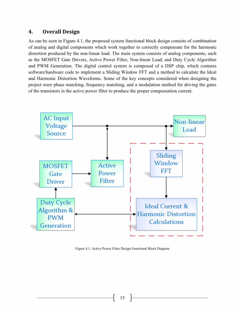
As can be seen in Figure 4.1, the proposed system functional block design consists of combination
of analog and digital components which work together to correctly compensate for the harmonic
distortion produced by the non-linear load. The main system consists of analog components, such
as the MOSFET Gate Drivers, Active Power Filter, Non-linear Load, and Duty Cycle Algorithm
and PWM Generation. The digital control system is composed of a DSP chip, which contains
software/hardware code to implement a Sliding Window FFT and a method to calculate the Ideal
and Harmonic Distortion Waveforms. Some of the key concepts considered when designing the
project were phase matching, frequency matching, and a modulation method for driving the gates
of the transistors in the active power filter to produce the proper compensation current.
Figure 4.1: Active Power Filter Design Functional Block Diagram
16
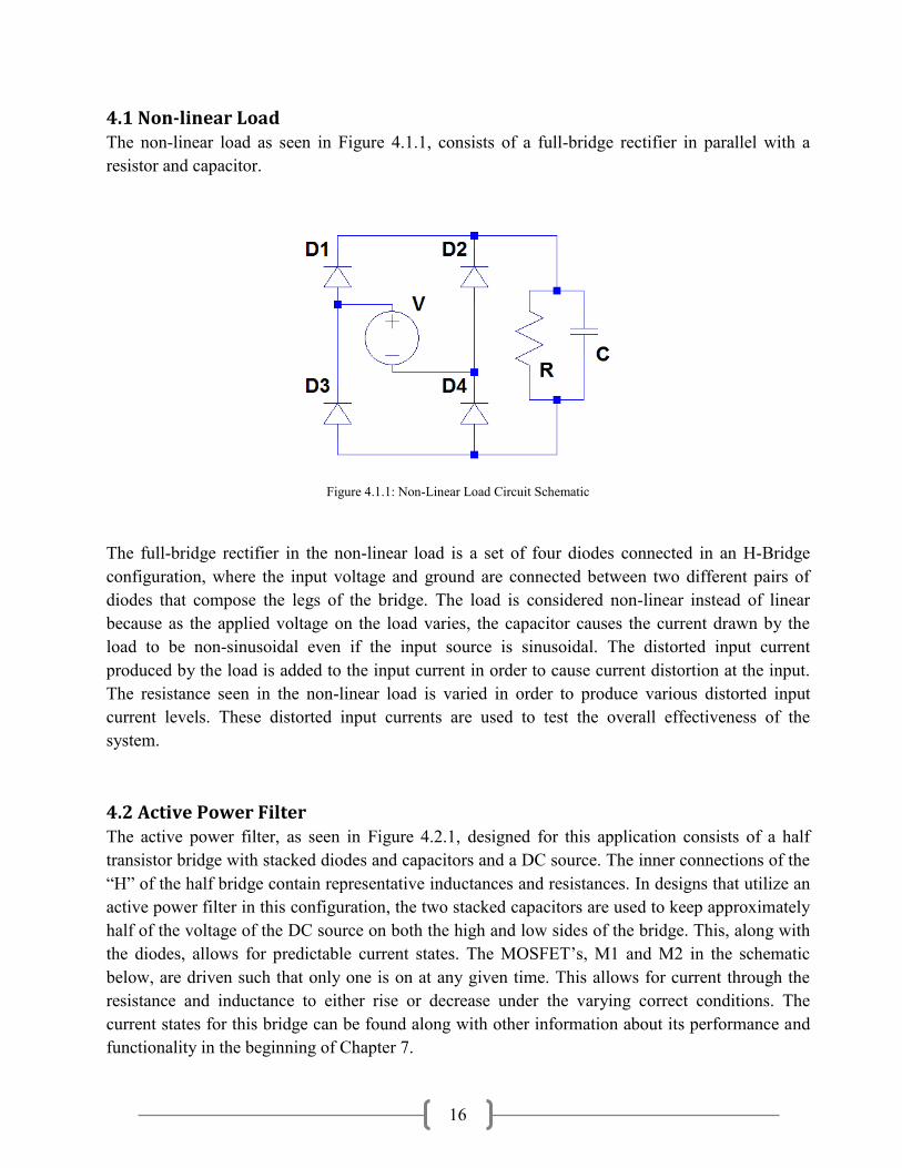
4.1 Non-linear Load The non-linear load as seen in Figure 4.1.1, consists of a full-bridge rectifier in parallel with a
resistor and capacitor.
Figure 4.1.1: Non-Linear Load Circuit Schematic
The full-bridge rectifier in the non-linear load is a set of four diodes connected in an H-Bridge
configuration, where the input voltage and ground are connected between two different pairs of
diodes that compose the legs of the bridge. The load is considered non-linear instead of linear
because as the applied voltage on the load varies, the capacitor causes the current drawn by the
load to be non-sinusoidal even if the input source is sinusoidal. The distorted input current
produced by the load is added to the input current in order to cause current distortion at the input.
The resistance seen in the non-linear load is varied in order to produce various distorted input
current levels. These distorted input currents are used to test the overall effectiveness of the
system.
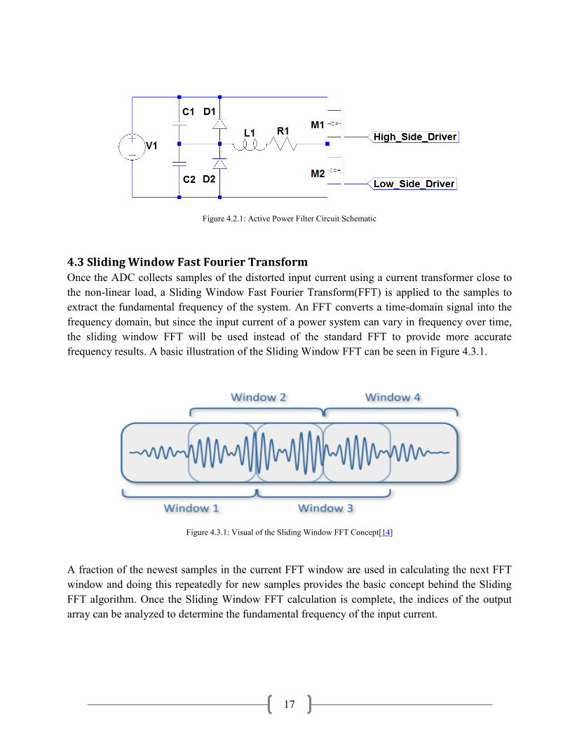
4.2 Active Power Filter The active power filter, as seen in Figure 4.2.1, designed for this application consists of a half
transistor bridge with stacked diodes and capacitors and a DC source. The inner connections of the
“H” of the half bridge contain representative inductances and resistances. In designs that utilize an
active power filter in this configuration, the two stacked capacitors are used to keep approximately
half of the voltage of the DC source on both the high and low sides of the bridge. This, along with
the diodes, allows for predictable current states. The MOSFET’s, M1 and M2 in the schematic
below, are driven such that only one is on at any given time. This allows for current through the
resistance and inductance to either rise or decrease under the varying correct conditions. The
current states for this bridge can be found along with other information about its performance and
functionality in the beginning of Chapter 7.
17
Figure 4.2.1: Active Power Filter Circuit Schematic
4.3 Sliding Window Fast Fourier Transform
Once the ADC collects samples of the distorted input current using a current transformer close to
the non-linear load, a Sliding Window Fast Fourier Transform(FFT) is applied to the samples to
extract the fundamental frequency of the system. An FFT converts a time-domain signal into the
frequency domain, but since the input current of a power system can vary in frequency over time,
the sliding window FFT will be used instead of the standard FFT to provide more accurate
frequency results. A basic illustration of the Sliding Window FFT can be seen in Figure 4.3.1.
Figure 4.3.1: Visual of the Sliding Window FFT Concept[14]
A fraction of the newest samples in the current FFT window are used in calculating the next FFT
window and doing this repeatedly for new samples provides the basic concept behind the Sliding
FFT algorithm. Once the Sliding Window FFT calculation is complete, the indices of the output
array can be analyzed to determine the fundamental frequency of the input current.

18
4.4 Ideal Current & Harmonic Distortion Calculations The Sliding FFT algorithm results in the determination of not only the fundamental frequency, but
also the magnitude and phase of the input current. Once these values are extracted, the sin function
from the math library can be used to reconstruct the ideal input current. The previous input current
sampled from the line is the distorted input current, which is used in calculating the harmonic
distortion waveform. The harmonic distortion waveform is used as a comparison waveform in the
Duty Cycle Algorithm and PWM Generation block.
4.5 Duty Cycle Algorithm & PWM Generation The duty cycle algorithm determines the duty cycle values of the PWM output waveforms, which
are necessary to produce the proper compensation current in the active power filter. The duty cycle
algorithm used here is relatively simple. An internal high-speed comparator inside the dsPIC33F
chip is used to automatically determine the proper duty cycle values of the PWM output produced
by the comparator. One of the inputs to the comparator is the harmonic distortion waveform, which
is the distorted input current produced by the non-linear load. The harmonic distortion waveform is
produced by a DAC inside the dsPIC33F chip. The other input to the comparator is a triangle wave
produced by the analog triangle wave generator, which is input through a pin on the dsPIC33F
chip. The frequency of the triangle wave can be increased, which would allow for smaller current
deviations to be seen in the compensation current.
4.6 MOSFET Gate Driver Due to the low voltage capability of the output of normal microcontrollers, such as the dsPIC33F
chip, which ranges from 3 volts to 3.6 volts, a component which steps up the voltage needs to be
used. In this case, the MOSFET gate driver takes the PWM output voltages from the comparator
and steps up the voltage to drive the gates of both the low-side and high-side MOSFET’s in the
active power filter. Since the MOSFET’s being used in the active power filter are both NMOS
transistors, the gate voltage of the high-side NMOS transistor needs to be approximately 10 volts
higher than the low-side NMOS transistor. In order to accomplish this, a MOSFET driver with a
bootstrap configuration is utilized to make sure the high-side MOSFET can be driven properly.
In order to set a constant reference voltage at the source of the high-side MOSFET, the supply
voltage from the MOSFET driver is used as the reference. The bootstrap configuration at the high-
side MOSFET has a capacitor connected between the supply voltage and the bias voltage of the
MOSFET gate driver and is in series with a diode. The combination of the storage charge
capability of the capacitor and the charge regulation of the diode allows the high-side gate voltage
to be kept anywhere between 10 volts to 20 volts higher than the source voltage of the MOSFET.
The use of the bootstrap configuration allows the high-side MOSFET to operate in the correct
region of operation, while the low-side MOSFET can be driven in relation to ground. The use of

19
the MOSFET gate driver allows the gates of the MOSFET’s in the active power filter to be
properly driven by stepping up the voltage from the dsPIC33F microcontroller.[15]
5. System Specifications
Since the active power filter for this project is a proof of concept design, lower current and
voltages values were used to simulate the effect of the filter on the efficiency of a power system.
The maximum voltage chosen for the design of the project was 50 volts, while the maximum
current chosen for the design was two amperes. The maximum power dissipation for each portion
of the design was found through the completion of PSIM simulations of the active power filter
system design. The maximum power dissipation in the non-linear load was determined to be three
watts. In addition to the system specifications, since the design is a proof of concept design which
would be tested in breadboards, each of the components selected for the design needed to have a
DIP pin configuration also known as a through-hole configuration. All of the components selected
for the design were found using the previously stated system specifications and the through-hole
configuration as search filter parameters.
Most of the components used for the active power filter design were basic circuit components,
such as resistors, capacitors, inductors, and diodes, which were chosen for the design based upon
the voltage, current, and power dissipation ratings defined for the system. The desired values for
the resistors, capacitors, and inductors in the design were determined based upon the simulation
results. On the other hand, there were a couple components which were carefully selected based
upon the initial system requirements.
5.1 MOSFET’s
The first of these carefully searched components were the MOSFET’s. The singular MOSFET’s
were chosen over the IGBT and MOSFET H-bridge modules and the singular IGBT’s due to their
cost being much lower. The parameters used to perform the value analysis for the MOSFET’s can
be seen in Table 1.
20
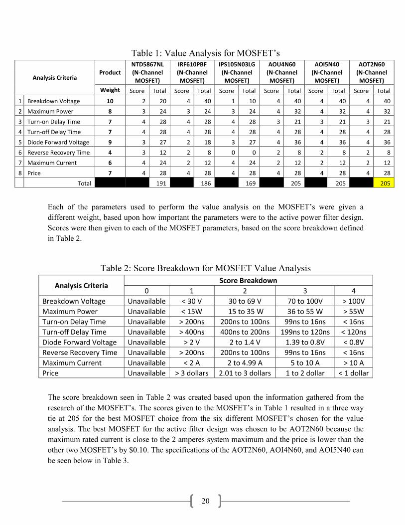
Table 1: Value Analysis for MOSFET’s
Analysis Criteria Product
NTD5867NL (N-Channel MOSFET)
IRF610PBF (N-Channel MOSFET)
IPS105N03LG (N-Channel MOSFET)
AOU4N60 (N-Channel MOSFET)
AOI5N40 (N-Channel MOSFET)
AOT2N60 (N-Channel MOSFET)
Weight Score Total Score Total Score Total Score Total Score Total Score Total
1 Breakdown Voltage 10 2 20 4 40 1 10 4 40 4 40 4 40
2 Maximum Power 8 3 24 3 24 3 24 4 32 4 32 4 32
3 Turn-on Delay Time 7 4 28 4 28 4 28 3 21 3 21 3 21
4 Turn-off Delay Time 7 4 28 4 28 4 28 4 28 4 28 4 28
5 Diode Forward Voltage 9 3 27 2 18 3 27 4 36 4 36 4 36
6 Reverse Recovery Time 4 3 12 2 8 0 0 2 8 2 8 2 8
7 Maximum Current 6 4 24 2 12 4 24 2 12 2 12 2 12
8 Price 7 4 28 4 28 4 28 4 28 4 28 4 28
Total 191 186 169 205 205 205
Each of the parameters used to perform the value analysis on the MOSFET’s were given a
different weight, based upon how important the parameters were to the active power filter design.
Scores were then given to each of the MOSFET parameters, based on the score breakdown defined
in Table 2.
Table 2: Score Breakdown for MOSFET Value Analysis
Analysis Criteria Score Breakdown
0 1 2 3 4
Breakdown Voltage Unavailable < 30 V 30 to 69 V 70 to 100V > 100V
Maximum Power Unavailable < 15W 15 to 35 W 36 to 55 W > 55W
Turn-on Delay Time Unavailable > 200ns 200ns to 100ns 99ns to 16ns < 16ns
Turn-off Delay Time Unavailable > 400ns 400ns to 200ns 199ns to 120ns < 120ns
Diode Forward Voltage Unavailable > 2 V 2 to 1.4 V 1.39 to 0.8V < 0.8V
Reverse Recovery Time Unavailable > 200ns 200ns to 100ns 99ns to 16ns < 16ns
Maximum Current Unavailable < 2 A 2 to 4.99 A 5 to 10 A > 10 A
Price Unavailable > 3 dollars 2.01 to 3 dollars 1 to 2 dollar < 1 dollar
The score breakdown seen in Table 2 was created based upon the information gathered from the
research of the MOSFET’s. The scores given to the MOSFET’s in Table 1 resulted in a three way
tie at 205 for the best MOSFET choice from the six different MOSFET’s chosen for the value
analysis. The best MOSFET for the active filter design was chosen to be AOT2N60 because the
maximum rated current is close to the 2 amperes system maximum and the price is lower than the
other two MOSFET’s by $0.10. The specifications of the AOT2N60, AOI4N60, and AOI5N40 can
be seen below in Table 3.

21
Table 3: MOSFET Ratings used for Value Analysis
Analysis Criteria
AOI4N60 (N-Channel MOSFET)
AOI5N40 (N-Channel MOSFET)
AOT2N60 (N-Channel MOSFET)
Value Value Value
1 Breakdown Voltage [V] 600 400 600
2 Maximum Power [W] 104 78 74
3 Turn-on Delay Time [ns] 17 16.5 17.2
4 Turn-off Delay Time [ns] 34 24 27
5 Diode Forward Voltage [V] 0.76-1 0.77-1 0.79-1
6 Reverse Recovery Time [ns] 150-230 125-200 154-185
7 Maximum Current [A] 2.6-4 2.8-4.2 1.7-2
8 Price [$] 0.80 0.81 0.70
5.2 Digital Microcontroller The second of these carefully searched components was the digital microcontroller. Originally the
choice for digital microcontrollers was between a FPGA, a standard microcontroller(MCU), and a
digital signal processing(DSP) chip. First of all, the group had no experience using FPGA’s, so the
FPGA was the first option ruled out. Secondly, most standard MCU chips are not capable of
performing real-time DSP applications, such as power factor correction, so the DSP chip was
chosen as the proper chip for the active power filter application. Based on the digital control
requirements previously discussed, a set of specifications was defined to help in the selection of a
microcontroller for the active power filter design and can be seen in Table 4.
Table 4: Specifications for Digital Control
Digital Control Specifications Values
CPU Speed (MIPS) > 40
Operating Voltage Range (V) 3 to 3.6
# of ADC Modules >= 1
ADC Resolution (bits) >= 10
Successive Approximation Registers(SAR's) >= 2
PWM Outputs >= 4
PWM Resolution (bits) 16
# of DAC Modules >= 1
DAC Resolution (bits) >= 10
# of Timer Modules >= 2
*RAM (bytes) >= 8192
*Program Memory (kilobytes) >= 16
Pin Count <= 28 *Parameters were not included in the original chip selection, were added for selection of second chip.
22
The DSP chips come in two different data formats, which include floating point and fixed-point. A
floating point chip has an architecture which allows for floating point arithmetic and has 32-bit
containers of type float. The float data type can represent any decimal or integer value between
±3.4x1038
and ±1.2x10-38
. Since floats have such a large dynamic range, mathematical operations
using the float data type allow for almost infinite precision. The process of coding through the use
of floating point arithmetic is also quite easy and straightforward. However, the major drawback to
floating point chips is that in order to do these floating point mathematical operations quickly,
there needs to be dedicated floating point hardware available on the chip. For most floating point
architectures this hardware is quite expensive. Therefore a more reasonable low-cost alternative
would be a fixed-point chip. The major downside to fixed-point architectures is that they only
support fixed-point arithmetic and are normally limited to 16-bit containers. Since the containers to
store data are only 16 bits in size, instead of 32 bits or larger, the chips have limited precision,
which causes a major tradeoff between overflow and precision. This tradeoff becomes prominent
when carrying out mathematical operations where the result can be larger than either of the two
variables used in calculating the result.
The two mathematical operations which need to be taken into consideration are multiplication and
addition. For integer multiplication, the total number of bits found in the product is represented by
Equation 5.2.1.[16]
(5.2.1)
In order to make sure overflow does not occur in the multiplication step, the calculation of the
number of bits from Equation 5.2.1 cannot exceed the container bit limit of 16. For instance if x
has 16 bits and y has 8 bits, the corresponding product would need a total of 23 bits to represent
the value. However, since the maximum number of representable bits is 16, seven bits need to be
“thrown away” to avoid overflow. The bits which need to be “thrown away” will come from the
equivalent number of shifts being applied to the two input variables. In order to avoid overflow
during the addition step, the number of bits which need to be shifted is determined by Equation
5.2.2.
⌈ ( )⌉ (5.2.2)
In Equation 5.2.2, the M represents the number of additions which will be performed. If there are
M additions, then the ceiling of the log base two of M would help to determine the total number of
bits which need to be shifted between the two variables before they are added together. Therefore
by shifting each of these values by the result calculated via Equation 5.2.2, the total summation
will not overflow and can be stored within the 16-bit container. In order to avoid overflow, a
carefully developed shifting scheme needs to be created.
Since fixed-point filters can only use integer math operations, floating point operations with
decimals cannot be calculated. Therefore in order to represent decimals in fixed-point notation, the
idea of fractional bits is introduced. For a binary number N bits long, an invisible decimal point is
placed somewhere within the binary number to denote a certain level of precision. The interesting
23
part about precision in terms of a fixed point system is that the number of fractional bits precision
can be larger than the number of bits in the variable and can also be a negative number. Since the
decimal is an imaginary idea, the user needs to keep track of the fractional bits to make sure the
shifting is carried out properly. The methods explained for shifting above are conservative and will
guarantee that there is no overflow in the results, allowing for accurate results to be seen. The
number of fractional bits is denoted using the Q-M format, where M is the number of fractional
bits within the binary number. This idea is important for integer multiplication because the number
of fractional bits in the product is defined by Equation 5.2.3.[16]
(5.2.3)
The number of fractional bits in the product is the addition of the fractional bits of the two input
variables, so the M in the Q-M format helps to easily understand how many fractional bits will be
seen in the product. This idea is also important for integer addition because the number of
fractional bits for the sum should be the same as the two inputs. Therefore if the two inputs into an
addition step do not have the same Q-M format, the two numbers will not be added properly
causing errors to be introduced into the system.
The other factor considered when optimizing fixed-point code is the idea of precision. The amount
of precision found in the system is determined by the number of fractional bits preserved
throughout the filtering process. When values are shifted to the right to avoid overflow a certain
amount of precision is lost because the fractional bits are shifted out. Losing precision in order to
prevent overflow losses creates a cost-benefit relationship between overflow and precision. In
order to maximize the result, the optimal balance between overflow prevention and precision loss
needs to be obtained.
There are two main companies who sell real-time DSP chips: Texas Instruments(TI) and
Microchip. Most if not all of Texas Instrument’s DSP chips use floating point architectures, while
all of Microchip’s DSP chips use fixed-point architectures. Based upon experience, the logical
choice would be to use a TI DSP chip in the design for three reasons: the TI Code Composer
Studio integrated development environment(IDE) is familiar, the chip would be easier to code, and
the chip would allow for higher data accuracy. However, due to the fact that the project was not
sponsored and the cost of the project falls back on the ECE Department at WPI, the cost difference
between the TI chips and Microchip chips is just too great. Therefore the decision was made to
select a Microchip DSP chip, which would meet the system requirements laid out in Table 4.
The original chip chosen for the project was the dsPIC33FJ16GS502 from the DSP33F family of
Microchip devices. The Microchip devices are programmed using the MPLAB IDE, but for this
project the newer version of MPLAB, MPLABX, was chosen due to its updated user interface and
the numerous tutorial videos found online. Once the chip was received, the MPLABX IDE was
officially setup, and the code was fixed for compilation bugs an issue arose with building the
project. Due to the size of the data structures which were necessary to produce accurate results,
there needed to be an adequate amount of data memory(RAM) to store all of these values.

24
However, the dsPIC33FJ16GS502 chip chosen lacked the appropriate amount of memory to store
these data structures. Therefore a search for a new chip, which could support the creation of these
large data structures needed to be carried out. In order to make sure the new chip chosen had
plenty of RAM; the new chip would need to have at least 4 times the amount of RAM. Since the
dsPIC33FJ16GS502 chip had only 2.048kB of RAM, a chip with upwards of 16kB would be ideal.
Even though the dsPIC33FJ16GS502 chip did not have enough RAM to support the
implementation, the device had all of the proper features and peripherals which were crucial to the
success of the project, so a chip with similar features was desirable.
In order to make sure the time which had been spent creating the hardware setup code used for the
dsPIC33FJ16GS502 chip was not a waste; a chip of the same family would have to be found. The
hope was that a chip from the dsPIC33F family would have similar registers, so when converting
the hardware setup code to this new chip most of the conversions would be one-to-one and not
many changes would have to be made. The other major limitation was the number of pins the
dsP33F chip could have because the prototyping board which was bought to assist in programming
the DSP chip could only program chips up to 28 pins in size. Therefore one of the limitations
which had to be applied to the search was finding a chip with no more than 28 pins.
By using Microchip’s database search engine, four chips were found which fit the specification
requirements as stated above. All four of these chips were very similar, but the main difference
was that each chip either had a high-resolution DAC or a high-resolution PWM module for motor
control applications, but not both. The chips which had the high-resolution DAC’s only had PWM
modules which were used for input capture. The chips which had the high-resolution PWM
module for motor control applications only had 4-bit, low-resolution DAC’s. This proposed a
dilemma in chip selection because the two duty cycle algorithm implementations under
consideration each needed either a high-resolution DAC or a high-resolution PWM for motor
applications. If the triangle waveform comparison algorithm was used, the dsPIC33FJ128GP802
chip with the high-resolution digital-to-analog convert would be chosen and if the more complex,
mathematically driven duty cycle algorithm was used, the dsPIC33FJ128MC802 chip with the
high-resolution PWM for motor applications would be chosen. Originally, the application of a
more complex, mathematically driven duty cycle algorithm was the goal, but after much
consideration it was determined the proof of concept triangle waveform comparison algorithm was
the better approach for the project. However, since the proper chips could not be acquired until the
later stages of the project, there was not an adequate amount of time to study the datasheet in order
to allow for a quick transition. Therefore the implementation portion of the paper was written
referencing the original dsPIC33FJ16G502 chip.
In addition to the digital microcontroller, a dsPIC prototyping development board was acquired, so
the project code could be downloaded to the microcontroller. The development board selected
from Microchip Technology was a 16-bit, 28-pin starter demo board with part number DM300027.
The development board has easy access header pins, so signals output from the dsPIC33F chip can
be easily sent to an analog circuit via jumper wires.

25
5.3 MOSFET Gate Driver
The final component which needed to be researched was the MOSFET Gate Driver. The output
voltage from the dsPIC33F microcontroller was not high enough to drive the gates of the
MOSFET’s in the active power filter, so a component which could step up the voltage was
necessary. One driver is used to provide the voltages necessary to drive both the high and low-side
MOSFET’s. For simplicity, the MOSFET Gate Drivers with 8 pins were preferred, so the
component would be easier to understand and less safety components would be necessary. The
other two contributing factors which led to the decision of the MOSFET Gate Driver were cost and
thoroughness of the datasheet. The MOSFET Gate Driver with the best price, 8 pins, and had the
most thorough datasheet was the IR2011.
6. Digital Control System Implementation
This section of the report will provide a more detailed overview of how each element in the digital
control system was implemented. If a deeper understanding of the variables used or a better
understanding of the code flow is desired please refer to the MQP program files found in
Appendices A, B, C, and D. The Constants_Globals_Prototypes.h file contains all of the
definitions for all of the constants, globals, and prototypes used in the program, the
Init_Functions(GS502).h file contains all of the hardware initialization code used to setup the
dsPIC33F chip, the MQP_Code.c file contains all of the code which comprises the main program,
and the Enum_States.h file contains the state variable used to control when the “filling” and
“processing” buffers can be switched in the program.
6.1 Main Clock & Auxiliary Clock Configuration
The main clock on the dsPIC33F chip was configured to be 40 Megahertz. This frequency is
obtained by using the Internal Fast RC (FRC) oscillator, which provides a 7.37 Megahertz clock
frequency, in conjunction with one of the hardware PLL modules found on the dsPIC33F chip. The
operating clock frequency of the device, Fcy, is calculated using Equation 6.1.1.
(6.1.1)
In Equation 6.1.1, Fosc is the output frequency of the PLL, Fin is the input frequency to the PLL,
M is the PLL feedback divisor, N1 is the prescale factor, and N2 is the postscale factor. The
relationship of how these factors are applied to the FRC oscillator input can be seen in Figure
6.1.1.
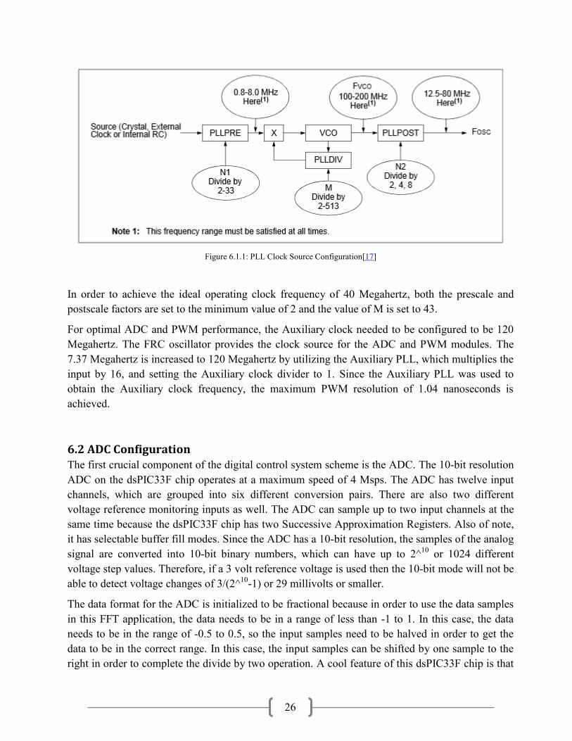
26
Figure 6.1.1: PLL Clock Source Configuration[17]
In order to achieve the ideal operating clock frequency of 40 Megahertz, both the prescale and
postscale factors are set to the minimum value of 2 and the value of M is set to 43.
For optimal ADC and PWM performance, the Auxiliary clock needed to be configured to be 120
Megahertz. The FRC oscillator provides the clock source for the ADC and PWM modules. The
7.37 Megahertz is increased to 120 Megahertz by utilizing the Auxiliary PLL, which multiplies the
input by 16, and setting the Auxiliary clock divider to 1. Since the Auxiliary PLL was used to
obtain the Auxiliary clock frequency, the maximum PWM resolution of 1.04 nanoseconds is
achieved.
6.2 ADC Configuration The first crucial component of the digital control system scheme is the ADC. The 10-bit resolution
ADC on the dsPIC33F chip operates at a maximum speed of 4 Msps. The ADC has twelve input
channels, which are grouped into six different conversion pairs. There are also two different
voltage reference monitoring inputs as well. The ADC can sample up to two input channels at the
same time because the dsPIC33F chip has two Successive Approximation Registers. Also of note,
it has selectable buffer fill modes. Since the ADC has a 10-bit resolution, the samples of the analog
signal are converted into 10-bit binary numbers, which can have up to 2^10
or 1024 different
voltage step values. Therefore, if a 3 volt reference voltage is used then the 10-bit mode will not be
able to detect voltage changes of 3/(2^10
-1) or 29 millivolts or smaller.
The data format for the ADC is initialized to be fractional because in order to use the data samples
in this FFT application, the data needs to be in a range of less than -1 to 1. In this case, the data
needs to be in the range of -0.5 to 0.5, so the input samples need to be halved in order to get the
data to be in the correct range. In this case, the input samples can be shifted by one sample to the
right in order to complete the divide by two operation. A cool feature of this dsPIC33F chip is that

27
the ADC is capable of completing pair conversions, which means the ADC is capable of
converting two different ADC channels at one time. This feature is made possible by the chip
having two successive approximation registers(SAR), where each SAR can convert a single
channel of the ADC. The ADC Conversion Pair 0 allows for the sampling of both CH0 and CH1 at
the same time, so in this case the ADC distorted load current is seen on CH0 and if a PLL
implementation was pursued then the PLL output could be seen on CH1.
In order to allow an interrupt to occur after both the CH0 and CH1 conversions take place, the
early interrupt is disabled. The ADC Conversion Pair 0 interrupt is given a priority of 6 out of 7,
where 7 is the highest priority user interrupt. The conversion of the ADC is triggered through the
use of a Timer1 period match as explained in the following Timer1 Configuration section.
6.3 Timer1 Configuration – ADC interrupts The period of the Timer1 module is derived from the internal operating clock frequency of the
dsPIC33F device, so the Timer1 period is defined as a specific number of internal clock cycles.
The value stored in the period match register for the Timer1 module was 3125, which was
determined by Equation 6.3.1.
(6.3.1)
In Equation 6.3.1, Ttimer1 is the desired Timer1 clock period, Nclock is the number of internal clock
cycles, and TCY is the period of the internal clock.
The Timer1 module is configured to be operating in Timer mode, so the Timer1 register will add
one to its count for each period of internal clock frequency until the value in the Timer1 register
matches the value of the Timer1 period register. When the values of these two registers match, the
count of the Timer1 register is reset to 0 and the counting process restarts. The ADC interrupts are
generated based upon a Timer1 period match, so when the Timer1 time base register reaches the
value of 3125 the ADC interrupt triggers. This allows the ADC interrupts to occur periodically at a
frequency of 12.8 kilohertz.
The 12.8 kilohertz sampling frequency not only allows for an accurate digital representation of the
input current, but it is also higher than the 2280 hertz frequency necessary to prevent aliasing of
the 19th
harmonic. The 19th
harmonic occurs at 1140 hertz, so in order to prevent aliasing the
sampling frequency needs to be at least twice that frequency according to the Nyquist Theorem, so
the minimum sampling frequency would be 2280 hertz. The input current is downsampled by 50,
in order to decrease the sampling frequency from 12.8 kilohertz to 256 hertz. The importance of
the downsampling exists in the relationship between the sampling frequency and the number of
points used in the FFT operation. Since a 256-point FFT is utilized and the input current signal was
downsampled to obtain a sampling frequency of 256 hertz, the frequency bins in the FFT operation
are one hertz apart. The one hertz resolution seen in the frequency bins of the FFT output should
be sufficient to produce an accurate representation of the fundamental frequency, magnitude, and
28
phase when reconstructing the ideal input current signal. If higher resolution frequency bins were
desired, this relationship could be adjusted to acquire frequency bins less than one hertz apart.
Another option would be to use a “fine search” algorithm, such as the Maximum Likelihood
Estimation algorithm, which acquires a more accurate estimate of the fundamental frequency,
magnitude, and phase of the input current through the extrapolation of the FFT output points.
6.4 Sliding Window FFT
The Sliding Window FFT implementation used in this project makes use of frame-by-frame
processing, where the ADC interrupt is used primarily to collect input samples and the main
function is where all of the samples are processed using the complex sliding FFT algorithm. While
the ADC is collecting samples to form frames, the main function is processing the previously filled
frame of samples. If the main function completes processing before the new frame in the ADC
interrupt is filled, then the system will be running in real-time.
The Sliding Window FFT algorithm makes use of two unique ideas which are crucial to the
program’s success, which are the data type fractcomplex and buffer memory alignment. The data
being stored in the buffers are complex, since it contains both real and imaginary parts. The
fractcomplex data type stores both the real and imaginary components in sequential memory
locations. In order for these buffers to process the samples properly in the main function, all of the
buffers involved with the FFT operation need to be aligned in memory. Therefore when the data in
the buffers is accessed at a particular index, the correct data is found at the corresponding memory
address. The buffers that are aligned are TwiddleF, ProcBuff, and FillBuff.
The basic structure of how the ISR and main code communicate in order to properly perform the
frame-by-frame processing for the Sliding FFT algorithm is depicted in the flow diagram seen in
Figure 6.4.1.
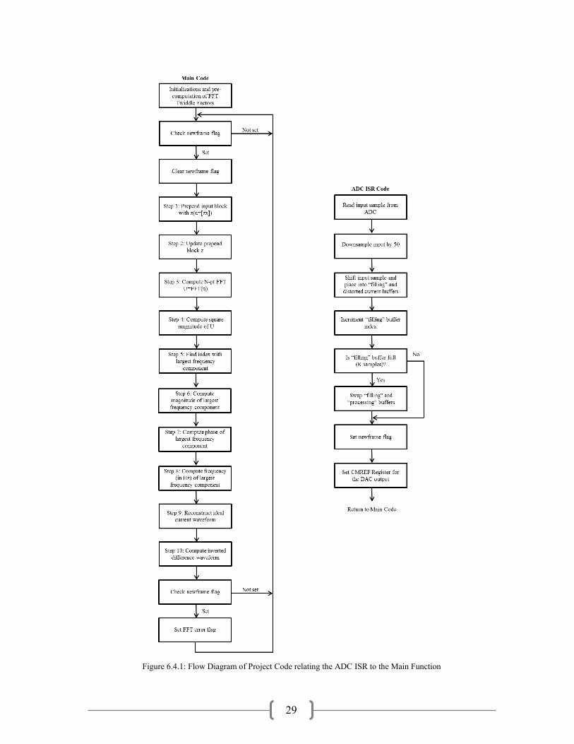
29
Figure 6.4.1: Flow Diagram of Project Code relating the ADC ISR to the Main Function
30
The basic structure of the main code is an if statement, which checks the new frame buffer flag to
see if there is a full buffer of samples that needs to be processed. Therefore the main code only
runs if there is a buffer which needs to be serviced. The if statement contains all of the code found
within the infinite while loop because all of this code is used in processing the ADC samples.
Inside the if statement, the new frame buffer flag is reset back to zero indicating the samples are
being serviced. Next, the Sliding FFT function is called to perform the sliding window FFT
operation with the frame of data coming from the ADC. Following the function call is an if
condition, which checks to see if the new frame buffer flag was set while the samples were being
processed. This condition is important because if the new frame buffer flag is set, then the ISR
improperly switched array pointers in the middle of a calculation which would cause data
corruption to occur. Therefore an error flag bit could be set, which would indicate the new frame
buffer flag had been updated in the ISR.
In any real-time system such as this one, the ISR can easily interrupt any calculations occurring in
the main function, so care has to be taken in order to make sure data corruption does not occur.
Therefore a form of state logic needs to be determined in order to make sure the ISR does not
switch array pointers when the program is running the main code critical section. In the
implementation, an enumeration state approach was taken to help prevent data corruption. An
enumeration variable, status, was defined to have one of four values: EMPTY, RDY, PROC, or
FIN. These values are state conditions which keep track of what the current status of the program
is at any point in time. The EMPTY state occurs when the buffer being passed to the ISR is empty
and has no samples in it. The RDY states occurs in the ISR when the buffer being filled has more
than zero samples in it, but less than K samples and the main function is not processing samples.
The PROC state is set as the first line in the Sliding FFT function, which tells the ISR that samples
are currently being processed and the ISR needs to wait until the processing is done to switch
buffer pointers as is explained later in the ISR section. The FIN state notifies the ISR when the
main code has completed processing the samples in the buffer. These states help track the progress
of the code in order to prevent data corruption in global variables which are accessed in critical
sections of code, such as in the main function of this code.
The main goal of the ISR is to acquire new samples from the ADC and switch the buffer pointers,
when the “filling” buffer is full and the “processing” buffer has been completely processed. In the
ISR, the sample coming from the channel one buffer of the 10-bit ADC is first stored into an ADC
result variable. The sampling frequency is downsampled by 50, so every 50th
sample is stored into
both the distorted input current and “filling” buffers. The variable keeping track of the
downsampling is initialized to zero, increments by one every iteration of the ISR, and is reset to
zero every time the variable reaches a value of 49.
In order to optimize precision in the calculation of the inverted difference equation later on, the
input sample being stored into the distorted input current buffer is kept at 10 bits and is not shifted.
The samples stored into the real component of the “filling” buffer, on the other hand, are shifted to
the right by two. There are two reasons to help explain why the shift is necessary. First, the FFT

31
input needs to be in the range of [-0.5, 0.5], so a shift of one from the initial range of [-1, 1] is
necessary. Second, the output of the FFT functions needs to fit within the 16-bit container. The
FFT function has an input buffer of 9-bit samples, which are each multiplied by the appropriate
twiddle factor. The worst case scenario product obtained from these multiplications should be 29.
If there are a total of 256 additions, then based on Equation 5.22 the total number of bits necessary
to store the result is 17 bits. Therefore since the container is only 16 bits, the input needs to be
shifted by one more to the right in order to obtain an output that has no overflow. Since the input
current is completely real, the imaginary component is set to zero.
A count variable is incremented every time a sample is added to both the distorted input current or
“filling” buffers in order to keep track of the number of samples being added to both buffers in the
ISR. When the “filling” buffer is full, the ISR can switch the buffer pointers. As long as the count
is less than or equal to K and the main is not processing samples, the status of the code is set to
RDY. The index variable, ind, controlling the indexing of the “filling” buffer is incremented each
time the ISR is run in order to update where the newest sample will be placed. If the “filling”
buffer is full and the main is not processing samples, ind is reset to be M-1, the count is reset to
zero, the buffer pointers are switched between the “filling” and “processing” buffers, the new
frame flag is set denoting the buffer is ready to be processed, and the status of the code is set to
EMPTY.
After the previous if statement, the data-ready bit for the Pair0 Interrupt is cleared, which allows
the ADC ISR to be reentered once exited. Next, the CMREF register of the DAC is set based upon
the oldest sample in OutBuff, which is found at the index denoted by the value of out_head. The
setting of the CMREF register is important because this value defines the output value of the DAC.
Therefore in this case, since the values of OutBuff are being used to define the DAC output, the
output of the DAC represents the harmonic distortion waveform. Since the OutBuff has a
maximum value of 1024, the maximum DAC equivalent output is 1.65 volts or AVDD/2.
The variable, out_head, is used to keep track of where the oldest sample in the output buffer is
located; while the variable out_tail is used to keep track of where the newest samples should be
placed in the output buffer. The value of out_head is incremented each time the ISR runs and is
also checked to see if it ever equals out_tail or the size of the output buffer. If out_head equals
out_tail, then at least one sample in the output buffer has been improperly overwritten and the data
has been corrupted. If this error was to propagate through the system, it would cause an incorrect
calculation in the duty cycle to occur, which would lead to an improper input current
compensation. Therefore as long as out_head and out_tail are never the same value, the system
should be running properly in real-time.
The Sliding FFT function first sets the status of the code to be PROC in order to tell the ISR
samples are being processed, so do not switch the buffer pointers. The index, ind_O, which tracks
the index at which samples are added to the output buffer is declared and initialized to zero. The
first for loop runs from 0 to M-2 and prepends the z[n] block of previous input samples to the new
x[n] input block, which is found in the “processing” buffer. The loop also stores the last M-1
32
samples in the “processing” buffer into the z[n] array to be used in the next iteration of the Sliding
FFT function.
Next, the FFT operation is performed on the “processing” buffer using the FFTComplexIP
function and the previously calculated Twiddle Factors. The FFTComplexIP function is an in-
place function, so the input buffer is used as the output buffer. Therefore in this case, the
“processing” buffer will also hold the output samples of the FFT operation. The FFTComplexIP
function also takes a natural index order buffer and outputs a result in a bit-reversed order.
Therefore in order to obtain a natural ordering of the data the BitReverseComplex function is
applied. The BitReverseComplex function takes the “processing” buffer and rearranges the FFT
output data into a natural ordering by bit-reversing the “processing” buffer data in order of its
addresses.
The bit-reversed output of the FFT found in the “processing” buffer has both real and imaginary
components, so in order to obtain a real output vector the SquareMagnitudeCplx function is
applied to each element of the “processing” buffer. This means that the real component and
imaginary component of each element in the “processing” buffer is squared, allowing all values
within the buffer to become real. The result of SquareMagnitudeCplx is stored in a temporary
buffer, B. Through the use of the VectorMax function, the index of the largest frequency
component in the B buffer is found. The magnitude of the input current is found in the B buffer at
the index of the largest frequency component. The phase of the input current is calculated using the
atan2 function on the complex data found at the index of the largest frequency component in the
“processing” buffer. The “processing” buffer used here still contains the output data of the FFT.
The fundamental frequency of the input current is found by multiplying the index of the largest
frequency component by the normalized downsampled ADC sampling rate, which is 256 hertz,
divided by the number of points in the FFT computation, 256.
The second for loop runs from 0 to K-1 and computes both the ideal current waveform and the
harmonic distortion waveform. The ideal current waveform is reconstructed through the use of the
sin function from the math library. The previously calculated fundamental frequency, phase, and
magnitude values are used in the sin function to produce the ideal input current. The variable,
out_tail, keeps track of where the last sample of the harmonic distortion waveform was placed in
the output buffer. Therefore when the newest K samples of the harmonic distortion waveform are
placed into the output buffer, they will be placed starting at the index value of out_tail, as indicated
by the value of ind_O. The value of ind_O is updated by adding the current value of the loop
control variable to its initial value of out_tail. The harmonic distortion waveform is calculated by
subtracting the distorted input current from the ideal current. Since the output buffer is a circular
array, ind_O is wrapped to the front of the array if its value exceeds the size of the output buffer.
The out_tail variable is updated to be the value at which the next processed sample from the main
function is placed. If this value exceeds the size of the output buffer, it is wrapped to the beginning
of the buffer. The final line changes the status of the code to FIN to tell the ISR the main code is
done processing the samples.

33
In this final for loop more accuracy can be obtained when creating the harmonic distortion
waveform by taking into account the time taken to run the digital control algorithm. If the design
had been implemented, the average number of clock cycles taken to run the program could be
calculated. If the average number of clock cycles was divided by the system clock frequency of 40
megahertz, then the time necessary to complete the program could be calculated. Since phase is
related to a shift in time, this value can be used in determining the proper ideal input current.
Therefore by using Equation 6.4.1, the time necessary to complete the program can be converted
into a phase angle.
(6.4.1)
In Equation 6.4.1, the θ term is the phase angle, the t term is the time required to complete the
program, and Ts is the sampling period. The phase value calculated here would have to be modulo
2π to make sure the phase is within one period of the input current signal. The phase calculated
here could be an extra phase component integrated into the portion of the program where the
harmonic distortion waveform is being determined.
6.5 Duty Cycle Algorithm & PWM Generation The goal of the final simulation completed for the active power filter design was to produce a
compensation current, which would properly remove the distorted input current from the input
current. Many active power filter applications utilize complex algorithms to provide accurate
compensation, where the total harmonic distortion of the input current is minimized; however,
many of these algorithms are out of the scope of this project because of how difficult they are to
implement. The purpose of all of the algorithms is to produce a set of inverted drive signals for the
gates of the transistors in the active power filter, which will provide accurate compensation
current. In order to reduce algorithm complexity, a simpler algorithm geared towards proof of
concept was developed for the active power filter design.
The simplified algorithm utilizes a comparator, which produces a square wave with a variable duty
cycle based upon the comparison between the two input signals. This PWM approach is known as
the intersective method, where a triangle wave is passed into the negative terminal of the
comparator and the harmonic distortion waveform is passed into the positive terminal of the
comparator. The square wave output of the comparator is high when the reference signal is at a
higher value than the triangle waveform and is low otherwise. The intersective method is a
simplified control method because the comparator automatically determines the proper duty cycles
for the MOSFET gate driving signals. One of the inputs to the comparator is the harmonic
distortion waveform, which is passed through a DAC before entering the comparator, and the
second input is a triangle waveform with an adjustable frequency. By increasing the frequency of
the triangle wave, the compensation current could more closely resemble the ideal because the
current deviation in the compensation current decreases. The triangle waveform could be produced
34
using two different methods, including: configuring a Timer module in up-down mode or a triangle
wave generator analog circuit. Since the original dsPIC33F chip chosen for the project did not
have an up-down mode for the Timer modules, a method of manually creating a triangle wave
through a count variable in an interrupt was the alternative option. Both the manual triangle wave
creation and analog triangle wave generator methods are analyzed below.
An attempt has been made to implement the first method of creating a triangle wave manually
through a count variable in an interrupt in order to replicate the results of the simulation. Since the
Timer2 and Timer3 modules in the dsPIC33F chip do not have up-down Timer modes, either
Timer2 or Timer3 needs to be manually converted from an up-mode timer into an up-down mode
timer. In order to implement the up-down mode timer, Timer2 is setup to run in timer mode and
the Timer2 interrupt is enabled. Since Timer2 and Timer3 can be combined to create a 32-bit
timer, the 32-bit Timerx Mode Select register was set to zero to allow Timer2 to be run as a 16-bit
timer. In order to make the translation from triangle wave to duty cycle percentage simple, the
number of values found in one half cycle of the triangle wave was chosen to be 99 from peak to
peak. Therefore each sample in the triangle waveform could represent a different duty cycle
percentage. The triangle waveform is formed through the use of the Timer2 interrupt, where a
count variable is incremented every time the interrupt occurs. The count variable starts at zero and
is incremented until it reaches a value of 100. The count variable is then set to 99 and then is
decremented until it reaches a value of zero. The count variable is then set to 1 and the process
repeats, creating the triangle waveform. The decision of whether to decrement or increment the
count is determined by a state variable, which tells whether the Timer is in up-mode or down-
mode.
The desired frequency of the triangle waveform is three kilohertz, so in order to obtain this
frequency a corresponding Timer2 frequency needs to be determined. The relationship between the
desired triangle wave frequency and the Timer2 frequency can be expressed through a proportion
as seen in Equation 6.5.1.
(6.5.1)
In Equation 6.5.1, FTri is the desired frequency of the triangle waveform, Ncycle is the number of
samples for one cycle of the triangle waveform, and FTimer2 is the frequency of Timer2.
If there are about 200 samples for one cycle of the desired three kilohertz frequency triangle
waveform, then the equivalent frequency of the Timer2 clock needs to be 600 kilohertz. The value
stored in the Timer2 period register is 66, which is calculated using Equation 6.4.1 for Timer2
instead of Timer1. The actual frequency of the triangle waveform would be 606,060 hertz
approximately, which is a bit higher than the ideal 600 kilohertz, so if a better approximation is
desired then the number of samples for one cycle of the triangle waveform would need to be
decreased.
The triangle waveform implementation seen here would work if the digital control was
implemented using sample-by-sample processing, but since frame-by-frame processing is used the
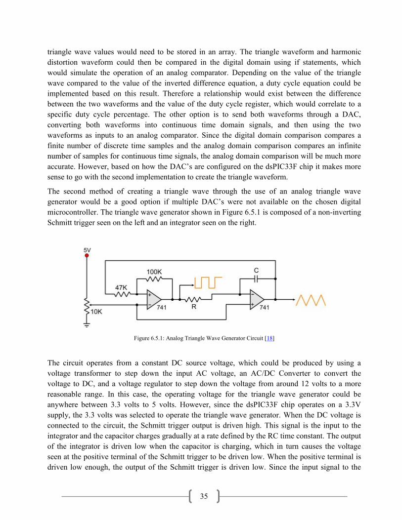
35
triangle wave values would need to be stored in an array. The triangle waveform and harmonic
distortion waveform could then be compared in the digital domain using if statements, which
would simulate the operation of an analog comparator. Depending on the value of the triangle
wave compared to the value of the inverted difference equation, a duty cycle equation could be
implemented based on this result. Therefore a relationship would exist between the difference
between the two waveforms and the value of the duty cycle register, which would correlate to a
specific duty cycle percentage. The other option is to send both waveforms through a DAC,
converting both waveforms into continuous time domain signals, and then using the two
waveforms as inputs to an analog comparator. Since the digital domain comparison compares a
finite number of discrete time samples and the analog domain comparison compares an infinite
number of samples for continuous time signals, the analog domain comparison will be much more
accurate. However, based on how the DAC’s are configured on the dsPIC33F chip it makes more
sense to go with the second implementation to create the triangle waveform.
The second method of creating a triangle wave through the use of an analog triangle wave
generator would be a good option if multiple DAC’s were not available on the chosen digital
microcontroller. The triangle wave generator shown in Figure 6.5.1 is composed of a non-inverting
Schmitt trigger seen on the left and an integrator seen on the right.
Figure 6.5.1: Analog Triangle Wave Generator Circuit [18]
The circuit operates from a constant DC source voltage, which could be produced by using a
voltage transformer to step down the input AC voltage, an AC/DC Converter to convert the
voltage to DC, and a voltage regulator to step down the voltage from around 12 volts to a more
reasonable range. In this case, the operating voltage for the triangle wave generator could be
anywhere between 3.3 volts to 5 volts. However, since the dsPIC33F chip operates on a 3.3V
supply, the 3.3 volts was selected to operate the triangle wave generator. When the DC voltage is
connected to the circuit, the Schmitt trigger output is driven high. This signal is the input to the
integrator and the capacitor charges gradually at a rate defined by the RC time constant. The output
of the integrator is driven low when the capacitor is charging, which in turn causes the voltage
seen at the positive terminal of the Schmitt trigger to be driven low. When the positive terminal is
driven low enough, the output of the Schmitt trigger is driven low. Since the input signal to the
36
integrator is now low, the capacitor in the integrator begins to discharge at the same rate defined
by the RC time constant. The discharging of the capacitor causes the integrator output to be driven
high, which in turn causes the voltage at the positive terminal of the Schmitt trigger to once again
be driven high allowing for the cyclical process to continue. This circuit behavior causes the output
of the Schmitt trigger to be a square wave with a constant duty cycle and the output of the
integrator to be a triangle wave with a constant frequency. The frequency of the triangle wave
oscillator can be determined by using Equation 6.5.2.
(6.5.2)
Through the careful selection of the resistor and capacitor values in the integrator, a particular
triangle wave frequency can be found. From a price and access standpoint, it may be easier to
select a particular capacitor which would be used in the circuit and then just change the resistor to
adjust the triangle wave frequency. There is a large dynamic range in resistor values, so many
frequencies could be achieved using a single capacitance value. For example, if a triangle wave
frequency of 2.5 kilohertz was desired a capacitor of 0.1 microfarads and a resistor of two
kiloohms could be used. The actual frequency value of the triangle waveform might differ from the
theoretical frequency value because of the 5% resistor and capacitor tolerances found in the
integrator. If the triangle wave output has a DC bias, a series capacitor can be added to the output
in order to remove the DC bias. Since the frequency range of the triangle wave is above one
kilohertz, a capacitor value in the range of nanofarads to picofarads might be ideal for the design to
avoid signal distortion.[18]
After the triangle wave and harmonic distortion waveform are passed through the comparator, the
output of the comparator is split into two different outputs. One of the two outputs is passed
through a “not” gate in order to invert the drive signal. By going through this process the high and
low-side MOSFET’s can be run in complementary mode. Even though the output of the
comparator was split in two to drive both high and low-side MOSFET’s, this will not cause a
current problem because the current necessary to drive MOSFET’s is very low.
6.6 Alternative Applications
Originally the idea for this project was to implement a duty cycle algorithm, which was derived
based on mathematics. This implementation would have required the use of the PWM module,
where the duty cycle register would be updated immediately based upon a duty cycle calculation in
order to produce the proper compensation current out of the active power filter. However, after
looking into many of the duty cycle algorithms they seemed to be quite complex in nature and
would be difficult to understand and implement. Another possible implementation was the fault
source PWM implementation, which would have automatically updated the PWM duty cycle
register by setting the fault pin. This design strayed away from some of the key concepts seen in
the simulation results for the project, so this implementation was kept as a future consideration.
Even though the implementation of the project went in a different direction, the original ideas for
37
the setup and coding of these designs have been included in order to give the reader a perspective
of how other duty cycle algorithms might have been implemented. The hardware initialization
codes are provided in the Init_Functions(GS502).h header file seen in Appendix B.
6.6.1 PWM Configuration The PWM module provides a pair of square wave control signals to the two MOSFET gates seen
in the active power filter of the design. The high and low-side MOSFET’s in the active power filter
cannot be “on” at the same time, so the PWM module is configured to be in complementary mode.
Complementary mode allows the pulse-width modulated drive signals for the high and low-side
MOSFET’s to be inverted versions of one another. For the purpose of this active power filter
design, only one PWM module is necessary to drive the two MOSFET gates seen in the half-
bridge implementation. If the full-bridge implementation were used, another PWM module would
be utilized to provide gate control signals for the second set of MOSFET’s. The duty cycles of
these pulse-width modulated signals would be calculated using a mathematically driven duty cycle
control algorithm or using a fault source pin duty cycle control algorithm. The pulse-width
modulated signals are output through the pins of the dsPIC33F chip and are sent directly to the
header pins of the development board. Through the use of jumper wires, the pulse-width
modulated signals seen at the header pins can be utilized in the analog portion of the design.
One alternative PWM implementation would be to use a mathematical duty cycle algorithm, which
could provide more accurate current compensation for more complex digital control algorithms. As
was described in the Main Clock & Auxiliary Clock Configuration section, the resolution of the
PWM module was initialized to be an optimal 1.04 nanoseconds. The resolution of the PWM
module was used in calculating the register values for the period of the PWM signal and the
deadtime using Equation 6.6.1.1.
(6.6.1.1)
In Equation 6.6.1.1, Rval is the value of the register, TDesired is the desired time for the register, and
Tres is the resolution of the PWM module.
The period of the PWM signal is limited by the switching frequency of the MOSFET’s in the
active power filter. Therefore since the maximum switching frequency is 50 kilohertz, which is
equivalent to 20 microseconds, the correct value for the PWM period register is 19,231. For this
application, the deadtime variable was deactivated, but if a time offset is necessary between the
two MOSFET drive signals then a value can be defined for the deadtime register.
The duty cycle of the PWM module output signal is determined using the PWM period previously
calculated. The duty cycle is a fraction of the PWM period, so in order to find the value for the
PWM duty cycle register a fraction of the PWM period register value needs to be used. For
instance, if a duty cycle of 50% is desired, then the duty cycle register would need to have value of
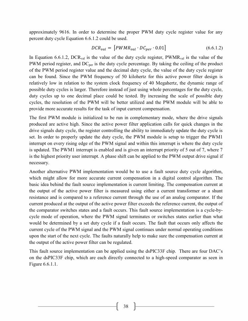
38
approximately 9616. In order to determine the proper PWM duty cycle register value for any
percent duty cycle Equation 6.6.1.2 could be used.
⌈ ⌉ (6.6.1.2)
In Equation 6.6.1.2, DCRval is the value of the duty cycle register, PWMRval is the value of the
PWM period register, and DCper is the duty cycle percentage. By taking the ceiling of the product
of the PWM period register value and the decimal duty cycle, the value of the duty cycle register
can be found. Since the PWM frequency of 50 kilohertz for this active power filter design is
relatively low in relation to the system clock frequency of 40 Megahertz, the dynamic range of
possible duty cycles is larger. Therefore instead of just using whole percentages for the duty cycle,
duty cycles up to one decimal place could be tested. By increasing the scale of possible duty
cycles, the resolution of the PWM will be better utilized and the PWM module will be able to
provide more accurate results for the task of input current compensation.
The first PWM module is initialized to be run in complementary mode, where the drive signals
produced are active high. Since the active power filter application calls for quick changes in the
drive signals duty cycle, the register controlling the ability to immediately update the duty cycle is
set. In order to properly update the duty cycle, the PWM module is setup to trigger the PWM1
interrupt on every rising edge of the PWM signal and within this interrupt is where the duty cycle
is updated. The PWM1 interrupt is enabled and is given an interrupt priority of 5 out of 7, where 7
is the highest priority user interrupt. A phase shift can be applied to the PWM output drive signal if
necessary.
Another alternative PWM implementation would be to use a fault source duty cycle algorithm,
which might allow for more accurate current compensation in a digital control algorithm. The
basic idea behind the fault source implementation is current limiting. The compensation current at
the output of the active power filter is measured using either a current transformer or a shunt
resistance and is compared to a reference current through the use of an analog comparator. If the
current produced at the output of the active power filter exceeds the reference current, the output of
the comparator switches states and a fault occurs. This fault source implementation is a cycle-by-
cycle mode of operation, where the PWM signal terminates or switches states earlier than what
would be determined by a set duty cycle if a fault occurs. The fault that occurs only affects the
current cycle of the PWM signal and the PWM signal continues under normal operating conditions
upon the start of the next cycle. The faults naturally help to make sure the compensation current at
the output of the active power filter can be regulated.
This fault source implementation can be applied using the dsPIC33F chip. There are four DAC’s
on the dsPIC33F chip, which are each directly connected to a high-speed comparator as seen in
Figure 6.6.1.1.
39
Figure 6.6.1.1: Comparator Module Block Diagram[17]
The multiplexer, seen in the top left of the diagram, can select one of four analog comparison
waveforms. In this application, the CMP1D pin is selected and corresponds to the compensation
current being measured at the output of the active power filter. The measured compensation
current is sent to the positive input of the internal comparator. The reference voltage selected for
the DAC, seen in the bottom left of the diagram, was chosen to be AVDD/2 or 1.65 volts. Since the
harmonic distortion waveform is the signal which needs to be compared to the measured
compensation current through the internal comparator, the value of the CMREF register needs to
be manipulated to mimic the harmonic distortion waveform. In this application, the harmonic
waveform needs to be inverted before being compared to the measured compensation current. In
the ADC interrupt, the CMREF register can be set to the value at the tail index of the output buffer,
which stores the calculated values of the harmonic distortion waveform. After setting the value of
the CMREF register, the output of the DAC can be determined by using Equation 6.6.1.3.
(
)
(6.6.1.3)
The harmonic distortion waveform output of the DAC could then be input into the negative input
terminal of the internal high-speed comparator. The internal high-speed comparator can then
compare the two waveforms, the measured compensation current and harmonic distortion
waveform, and produce a square wave pulse modulated signal which is split into two paths and one
of the paths has a “not” gate which produces an inverted PWM signal. Since the final simulation
for the active power filter design has the triangle wave being input into the negative terminal of the
comparator and the high-side does not have the “not” gate applied to it, the “not” gate path is
chosen to be the correct output of the internal high-speed comparator. The inverted PWM signal is
then used as the PWM duty cycle control, which helps to determine the proper duty cycle for the
complementary output signals produced by the PWM module.
40
The fault source output of the high-speed analog comparator is configured through the use of a
virtual pin. Therefore instead of having to use an additional physical I/O pin on the chip, an inter-
peripheral connection can be made using RP32, which connects the comparator output to the
PWM1 fault input. There are some other key differences between this implementation and the
mathematical duty cycle algorithm implementation. The fault source implementation does not
utilize the PWM interrupt, the immediate duty cycle register update capability is disabled, and the
comparator fault source output now provides the state for the PWM module instead of through the
updating of the duty cycle register. The duty cycle register value can be adjusted, if different
current responses are desired at the output of the active power filter. The other hardware
initialization ideas discussed in the mathematical duty cycle algorithm section all still apply here,
so please refer to that section for details regarding the rest of the initialization for this PWM
implementation.
7. Simulations
In order to gain a greater understanding of the APF system and design it is desirable to simulate
various conditions under which the system could operate. This gives much needed insight into the
feasibility and some of the complications that may arise down the line in construction. With this in
mind, PSPICE, PSIM, and Matlab were used to simulate various aspects of the APF design. The
analog implementation ranges from a look at the PSPICE voltage switch to the full APF system
with load in PSIM.
7.1 Digital Control Algorithm Simulation The digital control algorithm was simulated using Matlab to see if the thought process behind the
code worked properly. Since Matlab is completely software and does not contain any hardware
which needs to be initialized, it makes for a good testing platform. The digital control system
implementation explains most of the details about the Sliding FFT and duty cycle algorithms, but
the simulation differs in a few key areas. For the actual implementation, the ADC is used to sample
the distorted input current signal; however, Matlab has to generate the distorted input current
signal by using the definition of harmonics. The phase of the distorted input current is arbitrarily
set to zero for testing purposes, but if a more accurate value is desired than the phase shift caused
by the input inductance can be used. For example, an input inductance of a one millihenry
correlates to a 26.95 degree phase shift. The actual implementation also bounces back and forth
between the ADC ISR and the main function in order to process the samples, but in Matlab all of
the processing is done linearly. Due to this linearity, it does not make sense to implement a Sliding
FFT in Matlab, so a standard FFT function was used for simulation. Lastly, Matlab does not have a
fractional data-type, but Matlab can utilize both the double and 16-bit integer data-types to carry
out a fractional data-type implementation. Casting different variables in the program helps to
41
provide the proper data-types as were used in the actual program and also helps to allow the
Matlab functions to work properly, since some of the Matlab functions cannot operate on integer
data-types.
The procedure for the digital control algorithm simulation is described in the top of the code file
found in Appendix E, but will be expanded on here. The theoretical input current is produced using
the sin function at the ideal fundamental frequency of 60 hertz and the t array is based upon the
original sampling frequency of 12.8 hertz. The odd harmonics are calculated at the same sampling
frequency for the 3rd
harmonic through the 19th
harmonic and are added back to the theoretical
input current producing the distorted input current. The distorted input current is downsampled at a
rate of 50, which produces a signal with a corresponding sampling rate of 256 hertz. Similarly to
the actual implementation, two different versions of the distorted input current are produced. One
of the distorted input currents is a 10-bit signed integer value, which is used in later calculating the
harmonic distortion waveform and the other is an 8-bit signed integer value, which is used as the
input into the FFT function. In order to get both of these values to be either 10-bit or 8-bit, the
nextpow2 function is used to determine the optimum number of fractional bits that are required to
represent the values in the downsampled distorted input current. Therefore the values of the
downsampled distorted input current are converted to fit within the range of either 2^-10 to 2^10
or 2^-8 to 2^8.
The resolution of the FFT function can be calculated by dividing the sampling frequency used for
the signal being input into the FFT function by the number of points in the FFT. In this case, the
downsampled frequency is 256 hertz and there are 256 points in the FFT, so the FFT resolution is
one hertz. The 256-pt FFT function is applied to the 8-bit downsampled distorted input current and
the maximum of the FFT output is analyzed to see if the largest value would fit into a 16-bit
integer data-type. After being checked, the FFT output is separated into its real and imaginary parts
and are both stored as 16-bit signed integers. By utilizing the FFT output, the squared magnitude
can be calculated in order to determine where the maximum peak occurs in the frequency
response. Based on this information, the magnitude, phase, and fundamental frequency of the
distorted input current can be extracted. Next, the ideal input current is reconstructed using the
magnitude, phase, and fundamental frequency data extracted from the FFT output. This
reconstructed ideal input current is then made to fit within a 10-bit signed integer data-type and is
then used to calculate the harmonic distortion waveform. The 10-bit sampled distorted input
current is subtracted from the reconstructed ideal input current and is shifted by the size of a 10-bit
integer value to obtain the proper harmonic distortion waveform. The 10-bit shift is necessary
because the DAC on the dsPIC33F chip has a unipolar DAC, so negative values cannot be
represented. Therefore the harmonic distortion waveform is cast to be an unsigned 10-bit integer.
The digital control algorithm simulation was run using the parameters defined in Table 7, which
are also seen in Defined Parameters section of Appendix E.
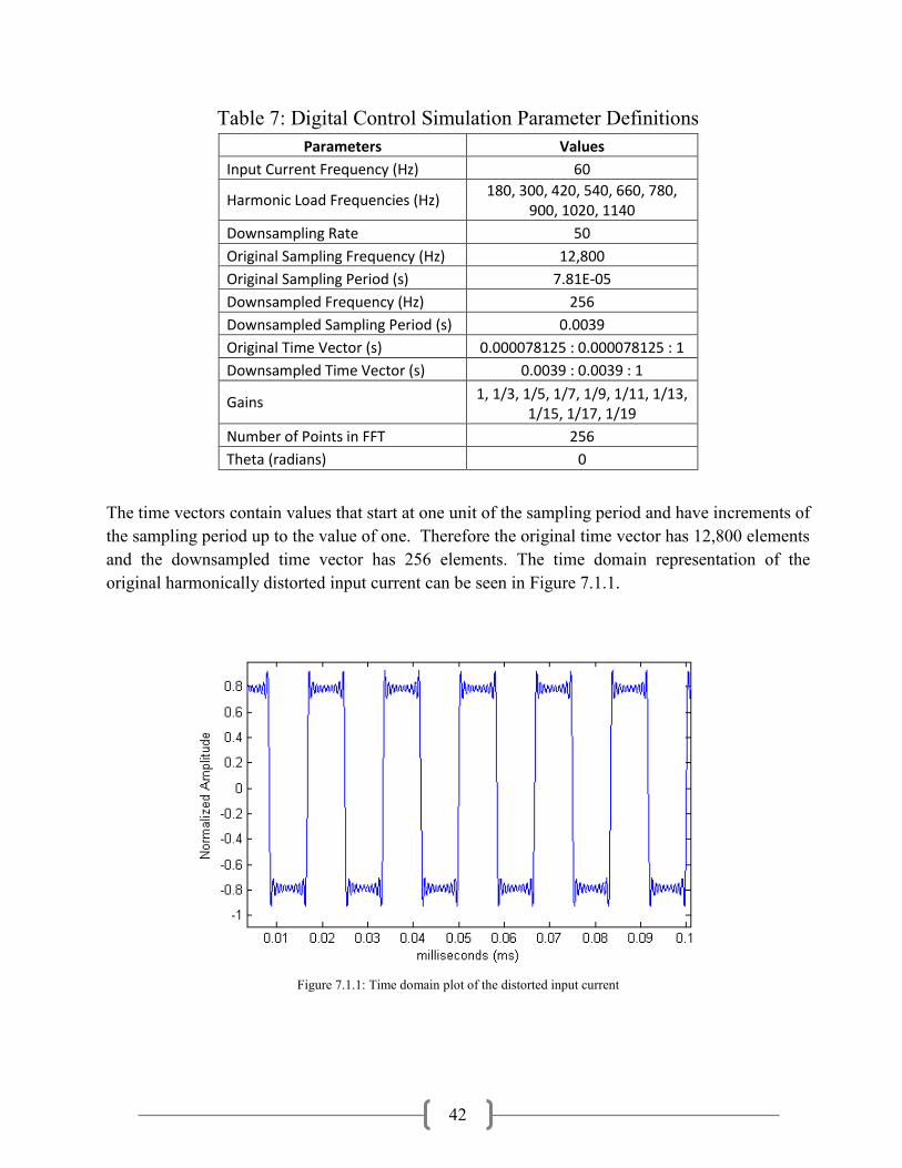
42
Table 7: Digital Control Simulation Parameter Definitions
Parameters Values
Input Current Frequency (Hz) 60
Harmonic Load Frequencies (Hz) 180, 300, 420, 540, 660, 780,
900, 1020, 1140
Downsampling Rate 50
Original Sampling Frequency (Hz) 12,800
Original Sampling Period (s) 7.81E-05
Downsampled Frequency (Hz) 256
Downsampled Sampling Period (s) 0.0039
Original Time Vector (s) 0.000078125 : 0.000078125 : 1
Downsampled Time Vector (s) 0.0039 : 0.0039 : 1
Gains 1, 1/3, 1/5, 1/7, 1/9, 1/11, 1/13,
1/15, 1/17, 1/19
Number of Points in FFT 256
Theta (radians) 0
The time vectors contain values that start at one unit of the sampling period and have increments of
the sampling period up to the value of one. Therefore the original time vector has 12,800 elements
and the downsampled time vector has 256 elements. The time domain representation of the
original harmonically distorted input current can be seen in Figure 7.1.1.
Figure 7.1.1: Time domain plot of the distorted input current
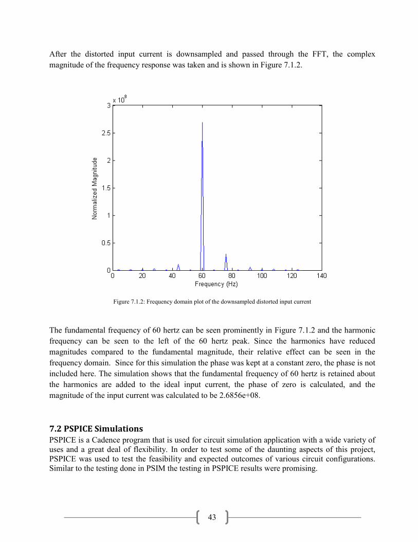
43
After the distorted input current is downsampled and passed through the FFT, the complex
magnitude of the frequency response was taken and is shown in Figure 7.1.2.
Figure 7.1.2: Frequency domain plot of the downsampled distorted input current
The fundamental frequency of 60 hertz can be seen prominently in Figure 7.1.2 and the harmonic
frequency can be seen to the left of the 60 hertz peak. Since the harmonics have reduced
magnitudes compared to the fundamental magnitude, their relative effect can be seen in the
frequency domain. Since for this simulation the phase was kept at a constant zero, the phase is not
included here. The simulation shows that the fundamental frequency of 60 hertz is retained about
the harmonics are added to the ideal input current, the phase of zero is calculated, and the
magnitude of the input current was calculated to be 2.6856e+08.
7.2 PSPICE Simulations PSPICE is a Cadence program that is used for circuit simulation application with a wide variety of
uses and a great deal of flexibility. In order to test some of the daunting aspects of this project,
PSPICE was used to test the feasibility and expected outcomes of various circuit configurations.
Similar to the testing done in PSIM the testing in PSPICE results were promising.
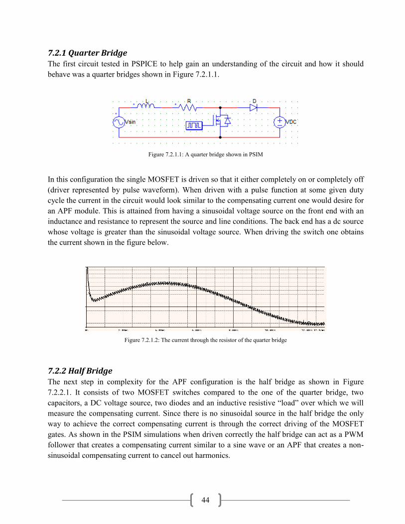
44
7.2.1 Quarter Bridge The first circuit tested in PSPICE to help gain an understanding of the circuit and how it should
behave was a quarter bridges shown in Figure 7.2.1.1.
Figure 7.2.1.1: A quarter bridge shown in PSIM
In this configuration the single MOSFET is driven so that it either completely on or completely off
(driver represented by pulse waveform). When driven with a pulse function at some given duty
cycle the current in the circuit would look similar to the compensating current one would desire for
an APF module. This is attained from having a sinusoidal voltage source on the front end with an
inductance and resistance to represent the source and line conditions. The back end has a dc source
whose voltage is greater than the sinusoidal voltage source. When driving the switch one obtains
the current shown in the figure below.
Figure 7.2.1.2: The current through the resistor of the quarter bridge
7.2.2 Half Bridge The next step in complexity for the APF configuration is the half bridge as shown in Figure
7.2.2.1. It consists of two MOSFET switches compared to the one of the quarter bridge, two
capacitors, a DC voltage source, two diodes and an inductive resistive “load” over which we will
measure the compensating current. Since there is no sinusoidal source in the half bridge the only
way to achieve the correct compensating current is through the correct driving of the MOSFET
gates. As shown in the PSIM simulations when driven correctly the half bridge can act as a PWM
follower that creates a compensating current similar to a sine wave or an APF that creates a non-
sinusoidal compensating current to cancel out harmonics.
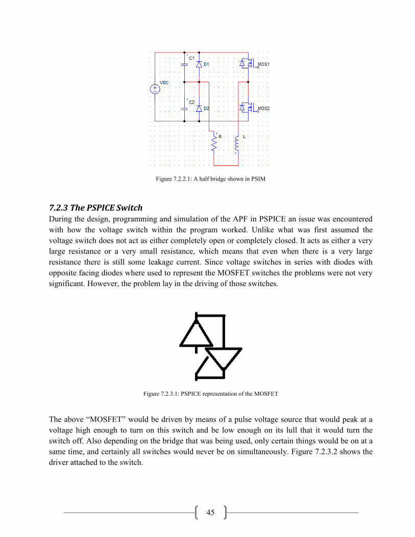
45
Figure 7.2.2.1: A half bridge shown in PSIM
7.2.3 The PSPICE Switch During the design, programming and simulation of the APF in PSPICE an issue was encountered
with how the voltage switch within the program worked. Unlike what was first assumed the
voltage switch does not act as either completely open or completely closed. It acts as either a very
large resistance or a very small resistance, which means that even when there is a very large
resistance there is still some leakage current. Since voltage switches in series with diodes with
opposite facing diodes where used to represent the MOSFET switches the problems were not very
significant. However, the problem lay in the driving of those switches.
Figure 7.2.3.1: PSPICE representation of the MOSFET
The above “MOSFET” would be driven by means of a pulse voltage source that would peak at a
voltage high enough to turn on this switch and be low enough on its lull that it would turn the
switch off. Also depending on the bridge that was being used, only certain things would be on at a
same time, and certainly all switches would never be on simultaneously. Figure 7.2.3.2 shows the
driver attached to the switch.
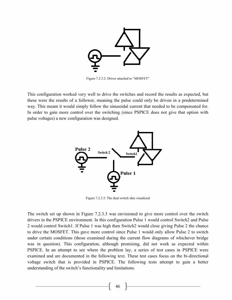
46
Figure 7.2.3.2: Driver attached to “MOSFET”
This configuration worked very well to drive the switches and record the results as expected, but
these were the results of a follower, meaning the pulse could only be driven in a predetermined
way. This meant it would simply follow the sinusoidal current that needed to be compensated for.
In order to gain more control over the switching (since PSPICE does not give that option with
pulse voltages) a new configuration was designed.
Figure 7.2.3.3: The dual switch idea visualized
The switch set up shown in Figure 7.2.3.3 was envisioned to give more control over the switch
drivers in the PSPICE environment. In this configuration Pulse 1 would control Switch2 and Pulse
2 would control Switch1. If Pulse 1 was high then Switch2 would close giving Pulse 2 the chance
to drive the MOSFET. This gave more control since Pulse 1 would only allow Pulse 2 to switch
under certain conditions (those examined during the current flow diagrams of whichever bridge
was in question). This configuration, although promising, did not work as expected within
PSPICE. In an attempt to see where the problem lay, a series of test cases in PSPICE were
examined and are documented in the following text. These test cases focus on the bi-directional
voltage switch that is provided in PSPICE. The following tests attempt to gain a better
understanding of the switch’s functionality and limitations.
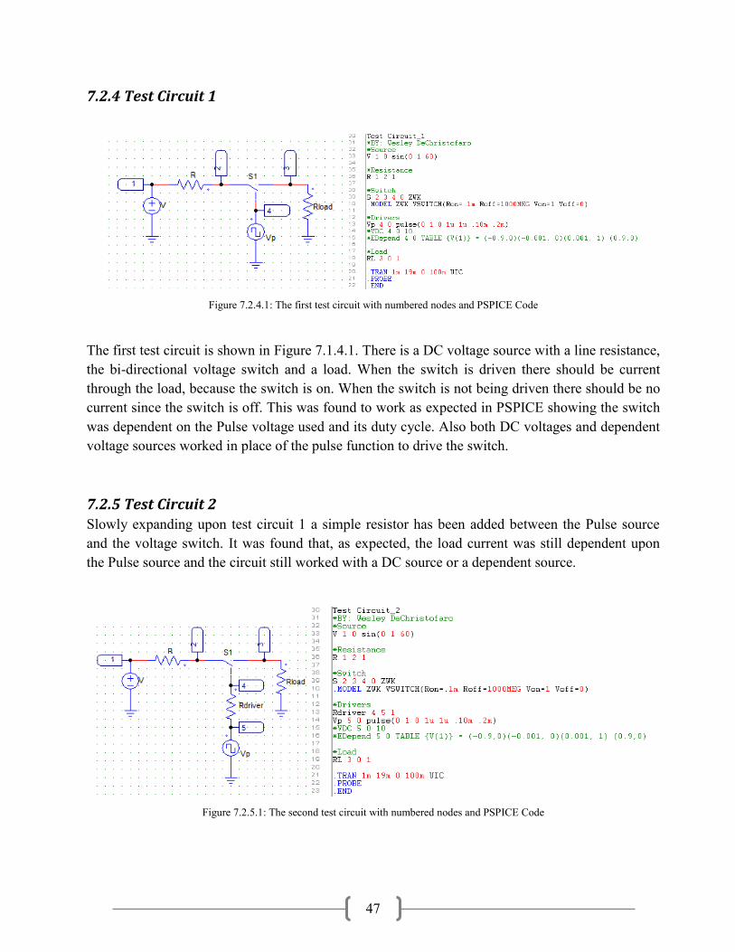
47
7.2.4 Test Circuit 1
Figure 7.2.4.1: The first test circuit with numbered nodes and PSPICE Code
The first test circuit is shown in Figure 7.1.4.1. There is a DC voltage source with a line resistance,
the bi-directional voltage switch and a load. When the switch is driven there should be current
through the load, because the switch is on. When the switch is not being driven there should be no
current since the switch is off. This was found to work as expected in PSPICE showing the switch
was dependent on the Pulse voltage used and its duty cycle. Also both DC voltages and dependent
voltage sources worked in place of the pulse function to drive the switch.
7.2.5 Test Circuit 2
Slowly expanding upon test circuit 1 a simple resistor has been added between the Pulse source
and the voltage switch. It was found that, as expected, the load current was still dependent upon
the Pulse source and the circuit still worked with a DC source or a dependent source.
Figure 7.2.5.1: The second test circuit with numbered nodes and PSPICE Code
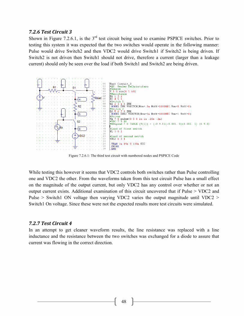
48
7.2.6 Test Circuit 3 Shown in Figure 7.2.6.1, is the 3
rd test circuit being used to examine PSPICE switches. Prior to
testing this system it was expected that the two switches would operate in the following manner:
Pulse would drive Switch2 and then VDC2 would drive Switch1 if Switch2 is being driven. If
Switch2 is not driven then Switch1 should not drive, therefore a current (larger than a leakage
current) should only be seen over the load if both Switch1 and Switch2 are being driven.
Figure 7.2.6.1: The third test circuit with numbered nodes and PSPICE Code
While testing this however it seems that VDC2 controls both switches rather than Pulse controlling
one and VDC2 the other. From the waveforms taken from this test circuit Pulse has a small effect
on the magnitude of the output current, but only VDC2 has any control over whether or not an
output current exists. Additional examination of this circuit uncovered that if Pulse > VDC2 and
Pulse > Switch1 ON voltage then varying VDC2 varies the output magnitude until VDC2 >
Switch1 On voltage. Since these were not the expected results more test circuits were simulated.
7.2.7 Test Circuit 4 In an attempt to get cleaner waveform results, the line resistance was replaced with a line
inductance and the resistance between the two switches was exchanged for a diode to assure that
current was flowing in the correct direction.
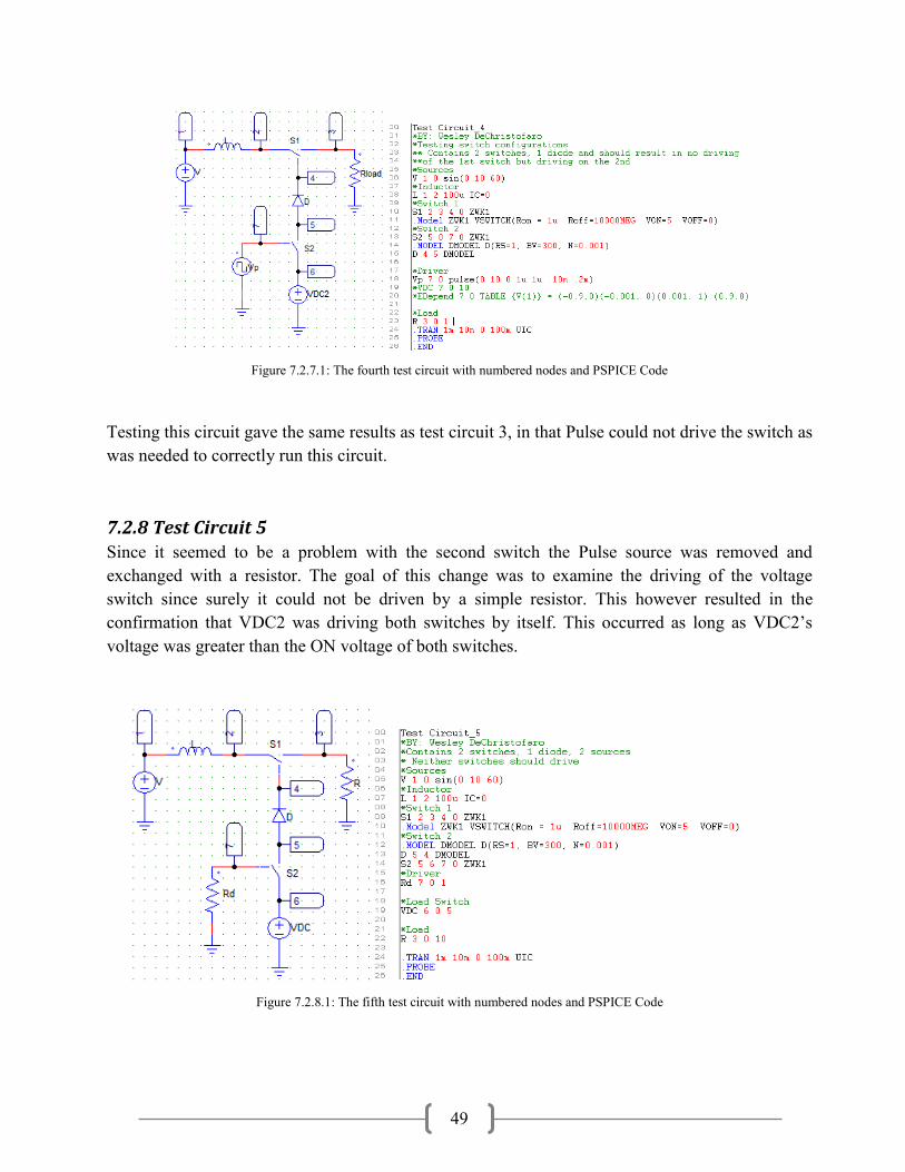
49
Figure 7.2.7.1: The fourth test circuit with numbered nodes and PSPICE Code
Testing this circuit gave the same results as test circuit 3, in that Pulse could not drive the switch as
was needed to correctly run this circuit.
7.2.8 Test Circuit 5
Since it seemed to be a problem with the second switch the Pulse source was removed and
exchanged with a resistor. The goal of this change was to examine the driving of the voltage
switch since surely it could not be driven by a simple resistor. This however resulted in the
confirmation that VDC2 was driving both switches by itself. This occurred as long as VDC2’s
voltage was greater than the ON voltage of both switches.
Figure 7.2.8.1: The fifth test circuit with numbered nodes and PSPICE Code
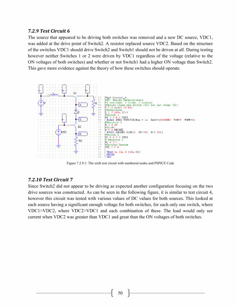
50
7.2.9 Test Circuit 6 The source that appeared to be driving both switches was removed and a new DC source, VDC1,
was added at the drive point of Switch2. A resistor replaced source VDC2. Based on the structure
of the switches VDC1 should drive Switch2 and Switch1 should not be driven at all. During testing
however neither Switches 1 or 2 were driven by VDC1 regardless of the voltage (relative to the
ON voltages of both switches) and whether or not Switch1 had a higher ON voltage than Switch2.
This gave more evidence against the theory of how these switches should operate.
Figure 7.2.9.1: The sixth test circuit with numbered nodes and PSPICE Code
7.2.10 Test Circuit 7
Since Switch2 did not appear to be driving as expected another configuration focusing on the two
drive sources was constructed. As can be seen in the following figure, it is similar to test circuit 4,
however this circuit was tested with various values of DC values for both sources. This looked at
each source having a significant enough voltage for both switches, for each only one switch, where
VDC1>VDC2, where VDC2>VDC1 and each combination of these. The load would only see
current when VDC2 was greater than VDC1 and great than the ON voltages of both switches.
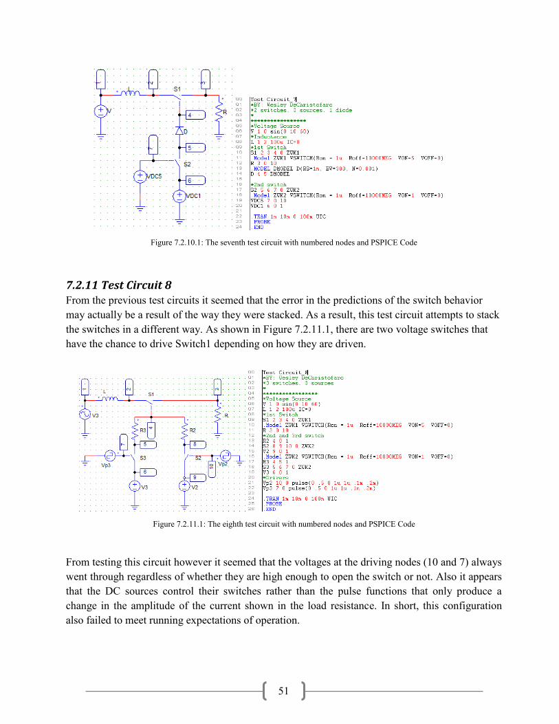
51
Figure 7.2.10.1: The seventh test circuit with numbered nodes and PSPICE Code
7.2.11 Test Circuit 8 From the previous test circuits it seemed that the error in the predictions of the switch behavior
may actually be a result of the way they were stacked. As a result, this test circuit attempts to stack
the switches in a different way. As shown in Figure 7.2.11.1, there are two voltage switches that
have the chance to drive Switch1 depending on how they are driven.
Figure 7.2.11.1: The eighth test circuit with numbered nodes and PSPICE Code
From testing this circuit however it seemed that the voltages at the driving nodes (10 and 7) always
went through regardless of whether they are high enough to open the switch or not. Also it appears
that the DC sources control their switches rather than the pulse functions that only produce a
change in the amplitude of the current shown in the load resistance. In short, this configuration
also failed to meet running expectations of operation.
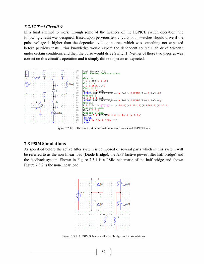
52
7.2.12 Test Circuit 9 In a final attempt to work through some of the nuances of the PSPICE switch operation, the
following circuit was designed. Based upon pervious test circuits both switches should drive if the
pulse voltage is higher than the dependent voltage source, which was something not expected
before pervious tests. Prior knowledge would expect the dependent source E to drive Switch2
under certain conditions and then the pulse would drive Switch1. Neither of these two theories was
correct on this circuit’s operation and it simply did not operate as expected.
Figure 7.2.12.1: The ninth test circuit with numbered nodes and PSPICE Code
7.3 PSIM Simulations As specified before the active filter system is composed of several parts which in this system will
be referred to as the non-linear load (Diode Bridge), the APF (active power filter half bridge) and
the feedback system. Shown in Figure 7.3.1 is a PSIM schematic of the half bridge and shown
Figure 7.3.2 is the non-linear load.
Figure 7.3.1: A PSIM Schematic of a half bridge used in simulations
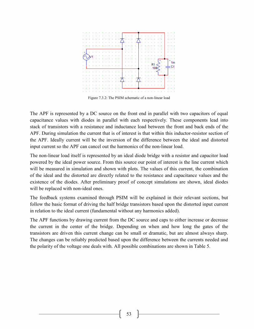
53
Figure 7.3.2: The PSIM schematic of a non-linear load
The APF is represented by a DC source on the front end in parallel with two capacitors of equal
capacitance values with diodes in parallel with each respectively. These components lead into
stack of transistors with a resistance and inductance load between the front and back ends of the
APF. During simulation the current that is of interest is that within this inductor-resistor section of
the APF. Ideally current will be the inversion of the difference between the ideal and distorted
input current so the APF can cancel out the harmonics of the non-linear load.
The non-linear load itself is represented by an ideal diode bridge with a resistor and capacitor load
powered by the ideal power source. From this source our point of interest is the line current which
will be measured in simulation and shown with plots. The values of this current, the combination
of the ideal and the distorted are directly related to the resistance and capacitance values and the
existence of the diodes. After preliminary proof of concept simulations are shown, ideal diodes
will be replaced with non-ideal ones.
The feedback systems examined through PSIM will be explained in their relevant sections, but
follow the basic format of driving the half bridge transistors based upon the distorted input current
in relation to the ideal current (fundamental without any harmonics added).
The APF functions by drawing current from the DC source and caps to either increase or decrease
the current in the center of the bridge. Depending on when and how long the gates of the
transistors are driven this current change can be small or dramatic, but are almost always sharp.
The changes can be reliably predicted based upon the difference between the currents needed and
the polarity of the voltage one deals with. All possible combinations are shown in Table 5.
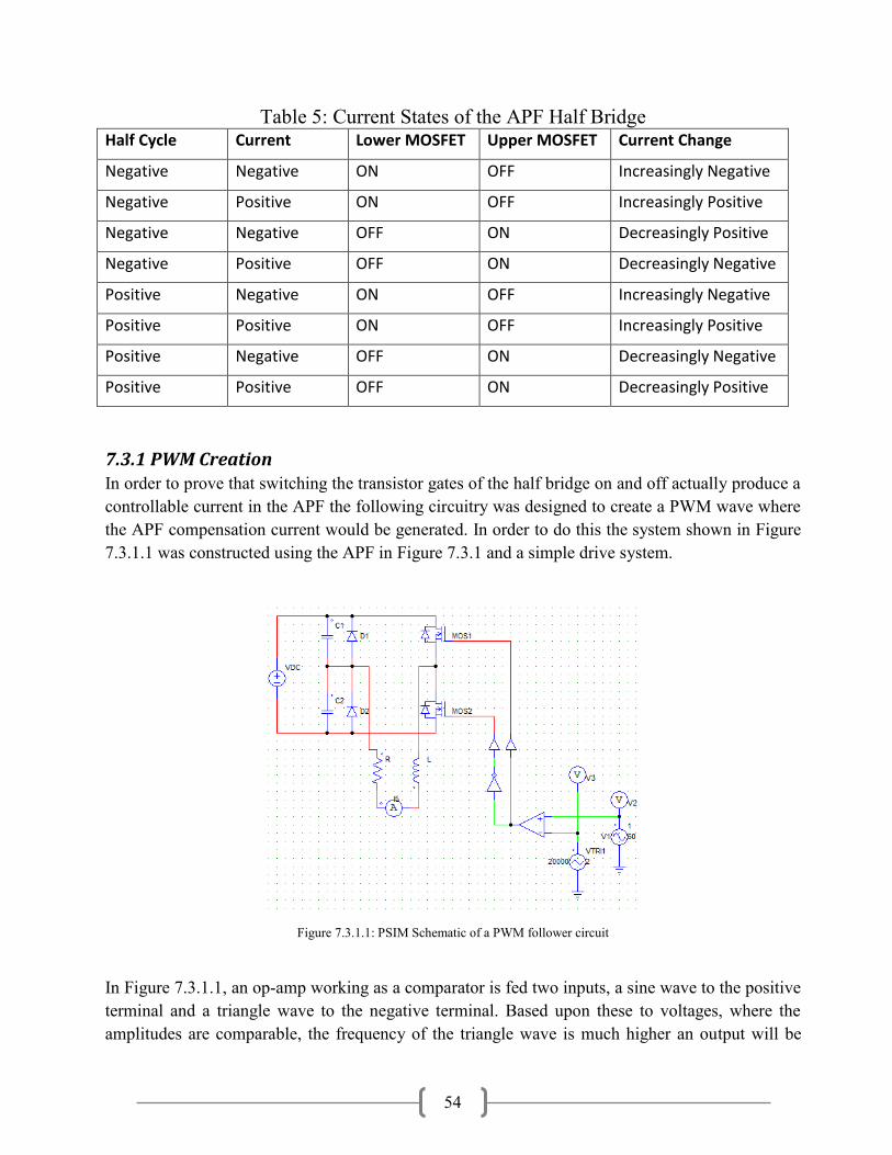
54
Table 5: Current States of the APF Half Bridge Half Cycle Current Lower MOSFET Upper MOSFET Current Change
Negative Negative ON OFF Increasingly Negative
Negative Positive ON OFF Increasingly Positive
Negative Negative OFF ON Decreasingly Positive
Negative Positive OFF ON Decreasingly Negative
Positive Negative ON OFF Increasingly Negative
Positive Positive ON OFF Increasingly Positive
Positive Negative OFF ON Decreasingly Negative
Positive Positive OFF ON Decreasingly Positive
7.3.1 PWM Creation In order to prove that switching the transistor gates of the half bridge on and off actually produce a
controllable current in the APF the following circuitry was designed to create a PWM wave where
the APF compensation current would be generated. In order to do this the system shown in Figure
7.3.1.1 was constructed using the APF in Figure 7.3.1 and a simple drive system.
Figure 7.3.1.1: PSIM Schematic of a PWM follower circuit
In Figure 7.3.1.1, an op-amp working as a comparator is fed two inputs, a sine wave to the positive
terminal and a triangle wave to the negative terminal. Based upon these to voltages, where the
amplitudes are comparable, the frequency of the triangle wave is much higher an output will be
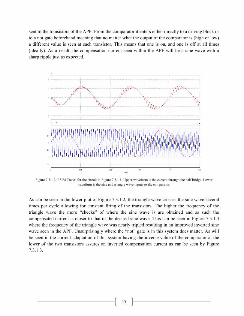
55
sent to the transistors of the APF. From the comparator it enters either directly to a driving block or
to a not gate beforehand meaning that no matter what the output of the comparator is (high or low)
a different value is seen at each transistor. This means that one is on, and one is off at all times
(ideally). As a result, the compensation current seen within the APF will be a sine wave with a
sharp ripple just as expected.
Figure 7.3.1.2: PSIM Traces for the circuit in Figure 7.3.1.1. Upper waveform is the current through the half bridge. Lower
waveform is the sine and triangle wave inputs to the comparator.
As can be seen in the lower plot of Figure 7.3.1.2, the triangle wave crosses the sine wave several
times per cycle allowing for constant firing of the transistors. The higher the frequency of the
triangle wave the more “checks” of where the sine wave is are obtained and as such the
compensated current is closer to that of the desired sine wave. This can be seen in Figure 7.3.1.3
where the frequency of the triangle wave was nearly tripled resulting in an improved inverted sine
wave seen in the APF. Unsurprisingly where the “not” gate is in this system does matter. As will
be seen in the current adaptation of this system having the inverse value of the comparator at the
lower of the two transistors assures an inverted compensation current as can be seen by Figure
7.3.1.3.
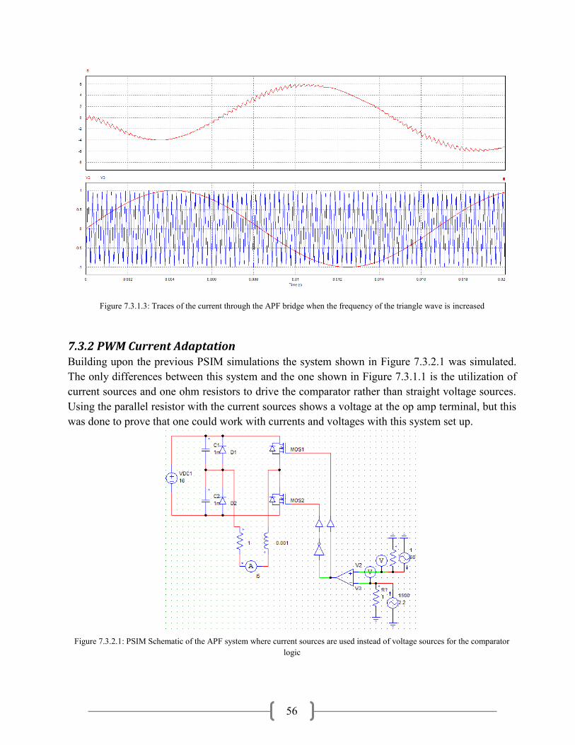
56
Figure 7.3.1.3: Traces of the current through the APF bridge when the frequency of the triangle wave is increased
7.3.2 PWM Current Adaptation Building upon the previous PSIM simulations the system shown in Figure 7.3.2.1 was simulated.
The only differences between this system and the one shown in Figure 7.3.1.1 is the utilization of
current sources and one ohm resistors to drive the comparator rather than straight voltage sources.
Using the parallel resistor with the current sources shows a voltage at the op amp terminal, but this
was done to prove that one could work with currents and voltages with this system set up.
Figure 7.3.2.1: PSIM Schematic of the APF system where current sources are used instead of voltage sources for the comparator
logic
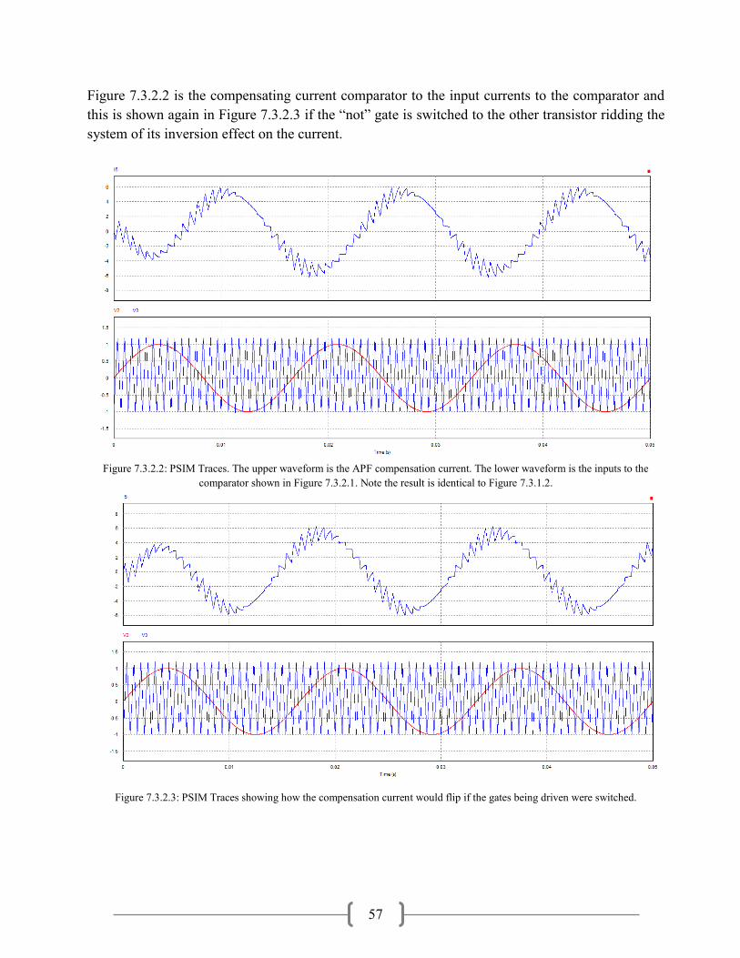
57
Figure 7.3.2.2 is the compensating current comparator to the input currents to the comparator and
this is shown again in Figure 7.3.2.3 if the “not” gate is switched to the other transistor ridding the
system of its inversion effect on the current.
Figure 7.3.2.2: PSIM Traces. The upper waveform is the APF compensation current. The lower waveform is the inputs to the
comparator shown in Figure 7.3.2.1. Note the result is identical to Figure 7.3.1.2.
Figure 7.3.2.3: PSIM Traces showing how the compensation current would flip if the gates being driven were switched.
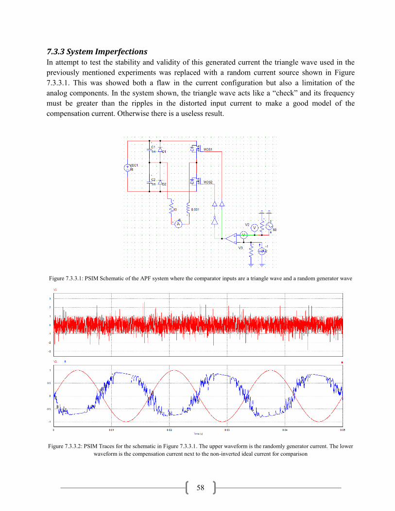
58
7.3.3 System Imperfections In attempt to test the stability and validity of this generated current the triangle wave used in the
previously mentioned experiments was replaced with a random current source shown in Figure
7.3.3.1. This was showed both a flaw in the current configuration but also a limitation of the
analog components. In the system shown, the triangle wave acts like a “check” and its frequency
must be greater than the ripples in the distorted input current to make a good model of the
compensation current. Otherwise there is a useless result.
Figure 7.3.3.1: PSIM Schematic of the APF system where the comparator inputs are a triangle wave and a random generator wave
Figure 7.3.3.2: PSIM Traces for the schematic in Figure 7.3.3.1. The upper waveform is the randomly generator current. The lower
waveform is the compensation current next to the non-inverted ideal current for comparison
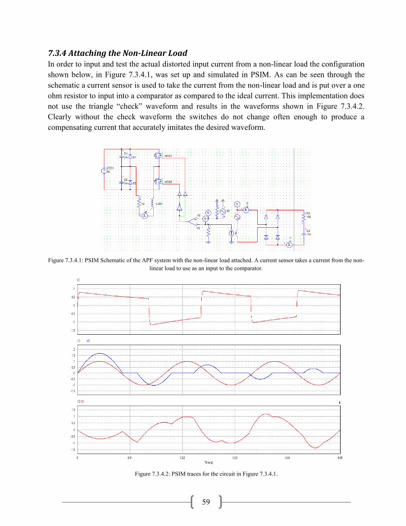
59
7.3.4 Attaching the Non-Linear Load In order to input and test the actual distorted input current from a non-linear load the configuration
shown below, in Figure 7.3.4.1, was set up and simulated in PSIM. As can be seen through the
schematic a current sensor is used to take the current from the non-linear load and is put over a one
ohm resistor to input into a comparator as compared to the ideal current. This implementation does
not use the triangle “check” waveform and results in the waveforms shown in Figure 7.3.4.2.
Clearly without the check waveform the switches do not change often enough to produce a
compensating current that accurately imitates the desired waveform.
Figure 7.3.4.1: PSIM Schematic of the APF system with the non-linear load attached. A current sensor takes a current from the non-
linear load to use as an input to the comparator.
Figure 7.3.4.2: PSIM traces for the circuit in Figure 7.3.4.1.
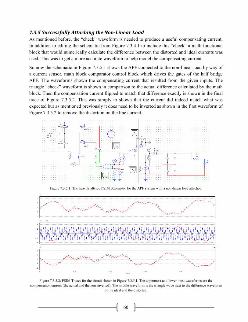
60
7.3.5 Successfully Attaching the Non-Linear Load As mentioned before, the “check” waveform is needed to produce a useful compensating current.
In addition to editing the schematic from Figure 7.3.4.1 to include this “check” a math functional
block that would numerically calculate the difference between the distorted and ideal currents was
used. This was to get a more accurate waveform to help model the compensating current.
So now the schematic in Figure 7.3.5.1 shows the APF connected to the non-linear load by way of
a current sensor, math block comparator control block which drives the gates of the half bridge
APF. The waveforms shown the compensating current that resulted from the given inputs. The
triangle “check” waveform is shown in comparison to the actual difference calculated by the math
block. Then the compensation current flipped to match that difference exactly is shown in the final
trace of Figure 7.3.5.2. This was simply to shown that the current did indeed match what was
expected but as mentioned previously it does need to be inverted as shown in the first waveform of
Figure 7.3.5.2 to remove the distortion on the line current.
Figure 7.3.5.1: The heavily altered PSIM Schematic for the APF system with a non-linear load attached.
Figure 7.3.5.2: PSIM Traces for the circuit shown in Figure 7.3.5.1. The uppermost and lower most waveforms are the
compensation current (the actual and the non-inverted). The middle waveform is the triangle wave next to the difference waveform
of the ideal and the distorted.
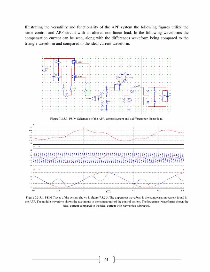
61
Illustrating the versatility and functionality of the APF system the following figures utilize the
same control and APF circuit with an altered non-linear load. In the following waveforms the
compensation current can be seen, along with the differences waveform being compared to the
triangle waveform and compared to the ideal current waveform.
Figure 7.3.5.3: PSIM Schematic of the APF, control system and a different non-linear load.
Figure 7.3.5.4: PSIM Traces of the system shown in figure 7.3.5.3. The uppermost waveform is the compensation current found in
the APF. The middle waveform shows the two inputs to the comparator of the control system. The lowermost waveforms shown the
ideal current compared to the ideal current with harmonics subtracted.

62
7.3.6 Issues with PSIM Simulations Of course there are some outstanding issues that result from the various simulations shown in the
section. First of these problems is of course the comparator block and the imperfections that would
exist here in the real world implementation. These vary from the losses across the resistor and it’s
variance in value from one ohm under different heating conditions. Second the functional block
that does the math function is not so easily implemented in analog as it is in a digital application.
Finally as can be seen by each and every waveform shown in this section there is a small phase
delay between the actual distortion and the compensation currents. This means that when the
compensation current is injected back into the line that the distortion may in fact increase in some
instances rather than decrease to zero. This long wall in the circuit progress is to be solved to our
DSP application described here within.
7.3.7 Summarized Functionality and Results
The main goal of the PSIM based circuit simulations was first a proof of concept and second an
examination at the imperfections and possible corrections we could make to the system. As
mentioned the first schematic utilized a full bridge that would be driven according to some set of
current flow conditions that would give the inverted compensation current for some given non-
linear load. Although this was fully possible it was desirable to have a more simple circuit and thus
the change to the half bridge shown above. This simpler circuit used half the MOSFETs, and had
easily discerned current flow models.
The basic function of the half bridge uses a current sensor to obtain the current from the non-linear
load. That current is compared with the ideal current (the reference) and the difference is
connected into the positive terminal of a binary operation amplifier (being the rails are irrelevant it
only sends an on or off signal). The negative terminal of the op-amp is connected to a high
frequency triangle wave that checks the difference wave at some predetermined rate. A higher
frequency here means greater precision in the compensation current found in the bridge. From the
operational amplifier the two MOSFET’s of the half bridge are in a complimentary arrangement
assuring that only one will be on at a time.
As can be seen from the waveform results given in the previous sections there is also the phase
shift of the compensation current waveform that is dependent upon the bridge inductance. A higher
inductance gives more phase difference. This difference can however be measured for a certain
inductance or corrected by an analog or digital PLL.

63
7.3.8 Additional PSIM Ideas Based upon the table shown in the previous section, a purely simplified system was designed in
PSIM. Since the environment has a maximum number of nodes that could be in operation at one
point the configuration was not fully texted, but based upon the aforementioned material it is
theorized that this following circuit would operate just as the analog bridge and op-amp
configuration. The binary conversion of the state table is shown here:
Table 6: Digital Adaptation of the Current States
Voltage = V Ideal Current =I1 Load Current = I2 Upper MOSFET Lower MOSFET
0 0 0 ON OFF
0 0 1 OFF ON
0 1 0 ON OFF
0 1 1 OFF ON
1 0 0 OFF OFF
1 0 1 OFF ON
1 1 0 ON OFF
1 1 1 OFF ON
In this world of thinking, the load current is the distorted input current from the non-linear load
and the ideal current is our goal current (or reference current). Voltage is represented as either high
or low, meaning either positive or negative and refers to the two different half cycles of the
sinusoidal wave.
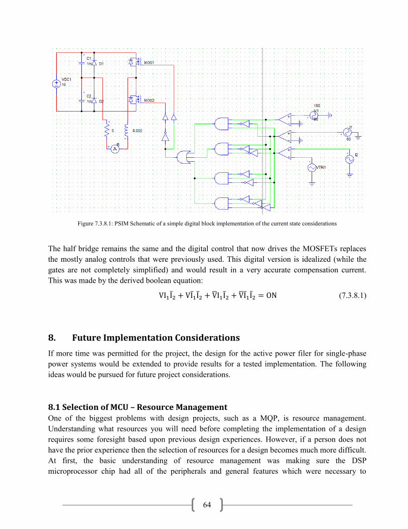
64
Figure 7.3.8.1: PSIM Schematic of a simple digital block implementation of the current state considerations
The half bridge remains the same and the digital control that now drives the MOSFETs replaces
the mostly analog controls that were previously used. This digital version is idealized (while the
gates are not completely simplified) and would result in a very accurate compensation current.
This was made by the derived boolean equation:
(7.3.8.1)
8. Future Implementation Considerations
If more time was permitted for the project, the design for the active power filer for single-phase
power systems would be extended to provide results for a tested implementation. The following
ideas would be pursued for future project considerations.
8.1 Selection of MCU – Resource Management One of the biggest problems with design projects, such as a MQP, is resource management.
Understanding what resources you will need before completing the implementation of a design
requires some foresight based upon previous design experiences. However, if a person does not
have the prior experience then the selection of resources for a design becomes much more difficult.
At first, the basic understanding of resource management was making sure the DSP
microprocessor chip had all of the peripherals and general features which were necessary to

65
implement the design. However, throughout the entire selection process there was one major
oversight which was the amount of data memory available on the chip.
During most of the digital courses at WPI, a student is normally told that the code written for any
lab project should fit within the amount of memory given. Therefore through each lab project, the
amount of memory at the disposal of the student was not something directly observed. This active
power filter project was no different; it was assumed that the amount of memory on the chip
obtained would be enough to implement the design. This ended up being a huge oversight, since
the amount of memory available on the chip was not enough to successfully build the program. If a
future implementation was pursued, the amount of data memory and program memory available on
the DSP microprocessor chip would definitely be a factor considered during the chip selection
process. Following the selection of the new DSP microprocessor chip, the code would be run,
debugged, modified, and tested to see if the proper PWM waveform or harmonic distortion
waveform was output from the device. Once the correct waveform is achieved, the DSP
microprocessor chip would be connected to the MOSFET Gate Driver to see if the correct voltage
levels would are seen at the output pins of the driver. Lastly, the MOSFET Gate Driver would be
directly connected to the gates of the transistors of the active power filter in order to see if the
correct compensation current is seen at the output line of the active power filter. Once all of these
stages are tested and debugged, the results would be tracked and written into the report.
8.2 Complex Duty Cycle Algorithms Many of the duty cycle control algorithms researched dealt with control engineering concepts,
which included power factor based algorithms, neural networks, voltage and current control loops,
or other complex mathematical algorithms. Since this project was a proof of concept active power
filter design, many of these ideas were beyond the scope of the project. However, if future
implementations were tested for more accurate input current compensation these algorithms would
be further looked into and possibly implemented to observe their effectiveness. Many of these
algorithms also dealt with sampling additional data from the circuit, including: the DC capacitor
voltage in the active power filter and the compensation current being produced by the active power
filter. If these values simply needed to be monitored in real-time, the high-speed analog
comparators paired with the DAC’s on the dsPIC33F could be used. These high-speed comparators
are coupled with their own personal DAC’s, so an analog comparison through the comparator can
be made comparing the sampled signal to a particular DC reference voltage.
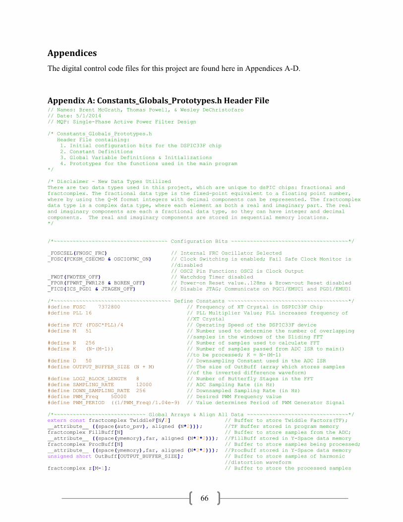
66
Appendices
The digital control code files for this project are found here in Appendices A-D.
Appendix A: Constants_Globals_Prototypes.h Header File // Names: Brent McGrath, Thomas Powell, & Wesley DeChristofaro
// Date: 5/1/2014
// MQP: Single-Phase Active Power Filter Design
/* Constants_Globals_Prototypes.h
Header File containing:
1. Initial configuration bits for the DSPIC33F chip
2. Constant Definitions
3. Global Variable Definitions & Initializations
4. Prototypes for the functions used in the main program
*/
/* Disclaimer - New Data Types Utilized
There are two data types used in this project, which are unique to dsPIC chips: fractional and
fractcomplex. The fractional data type is the fixed-point equivalent to a floating point number,
where by using the Q-M format integers with decimal components can be represented. The fractcomplex
data type is a complex data type, where each element as both a real and imaginary part. The real
and imaginary components are each a fractional data type, so they can have integer and decimal
components. The real and imaginary components are stored in sequential memory locations.
*/
/*~~~~~~~~~~~~~~~~~~~~~~~~~~~~~~~~~~~~ Configuration Bits ~~~~~~~~~~~~~~~~~~~~~~~~~~~~~~~~~~~~~*/
_FOSCSEL(FNOSC_FRC) // Internal FRC Oscillator Selected
_FOSC(FCKSM_CSECMD & OSCIOFNC_ON) // Clock Switching is enabled; Fail Safe Clock Monitor is
//disabled
// OSC2 Pin Function: OSC2 is Clock Output
_FWDT(FWDTEN_OFF) // Watchdog Timer disabled
_FPOR(FPWRT_PWR128 & BOREN_OFF) // Power-on Reset value..128ms & Brown-out Reset disabled
_FICD(ICS_PGD1 & JTAGEN_OFF) // Disable JTAG; Communicate on PGC1/EMUC1 and PGD1/EMUD1
/*~~~~~~~~~~~~~~~~~~~~~~~~~~~~~~~~~~~~~ Define Constants ~~~~~~~~~~~~~~~~~~~~~~~~~~~~~~~~~~~~~~*/
#define FOSC 7372800 // Frequency of XT Crystal in DSPIC33F Chip
#define PLL 16 // PLL Multiplier Value; PLL increases frequency of
//XT Crystal
#define FCY (FOSC*PLL)/4 // Operating Speed of the DSPIC33F device
#define M 51 // Number used to determine the number of overlapping
//samples in the windows of the Sliding FFT
#define N 256 // Number of samples used to calculate FFT
#define K (N-(M-1)) // Number of samples passed from ADC ISR to main()
//to be processed; K = N-(M-1)
#define D 50 // Downsampling Constant used in the ADC ISR
#define OUTPUT_BUFFER_SIZE (N + M) // The size of OutBuff (array which stores samples
//of the inverted difference waveform)
#define LOG2_BLOCK_LENGTH 8 // Number of Butterfly Stages in the FFT
#define SAMPLING_RATE 12000 // ADC Sampling Rate (in Hz)
#define DOWN_SAMPLING_RATE 256 // Downsampled Sampling Rate (in Hz)
#define PWM_Freq 50000 // Desired PWM Frequency value
#define PWM_PERIOD ((1/PWM_Freq)/1.04e-9) // Value determines Period of PWM Generator Signal
/*~~~~~~~~~~~~~~~~~~~~~~~~~~~~~ Global Arrays & Align All Data ~~~~~~~~~~~~~~~~~~~~~~~~~~~~~~~~*/
extern const fractcomplex TwiddleF[N/2] // Buffer to store Twiddle Factors(TF);
__attribute__ ((space(auto_psv), aligned (N*2))); //TF Buffer stored in program memory
fractcomplex FillBuff[N] // Buffer to store samples from the ADC;
__attribute__ ((space(ymemory),far, aligned (N*2*2))); //FillBuff stored in Y-Space data memory
fractcomplex ProcBuff[N] // Buffer to store samples being processed;
__attribute__ ((space(ymemory),far, aligned (N*2*2))); //ProcBuff stored in Y-Space data memory
unsigned short OutBuff[OUTPUT_BUFFER_SIZE]; // Buffer to store samples of harmonic
//distortion waveform
fractcomplex z[M-1]; // Buffer to store the processed samples
67
//from the previous frame calculation
fractional Ideal[K]; // Buffer to store samples for the ideal
//input current
fractional Dis_input[K]; // Buffer to store samples for the
//distorted input current
fractional B[N]; // Extra Buffer used in the Sliding FFT
//Function to store the Magnitude result
//char tri_wave[K]; // Count to produce 3.0kHz triangle wave
//(simulate timer's up-down mode)
/*~~~~~~~~~~~~~~~~~~~~~~~~~~~~~~~~~ Normal Global Variables ~~~~~~~~~~~~~~~~~~~~~~~~~~~~~~~~~~~*/
short ind = M-1; // Current index of "Filling" Buffer (location of newest sample)
short count = 0; // Keep track of the number of samples in the Distorted Input
//Current and "Filling" Buffers
char newframe_F = 0; // Flag to let user know when the "Filling" Buffer is full
fractcomplex *F; // Complex pointers used for switching between the starting
fractcomplex *P; //addresses of the ProcBuff and FillBuff Buffers
char M_Down = 0; // Variable to control Downsampling of the input current signal
//(Downsample by 50)
short i; // Loop control variable for all loops
short out_head = 1; // Keeps track of where the next sample to be output is stored in
//OutBuff (Updated in ISR)
short out_tail = 0; // Keeps track of what index the main code is writing to in OutBuff
short ADC_RSLT0 = 0; // Sample from ADC Channel 0
//short ADC_RSLT1 = 0; // Sample from ADC Channel 1
//(If Digital PLL was implemented this would be used!)
short peakFreqBin = 0; // Holds the index of the largest frequency component
unsigned long peakFreq = 0; // Value of the largest frequency component (in Hz)
//char udmode = 1; // Variable which controls the up-down mode in Timer2, creating the
//triangle wave
//char tri_count = 0; // Count used to produce 3.0kHz triangle wave
//(simulates a timer's up-down mode)
//char t_ind = 0; // Index of Triangle Waveform Buffer
char Error_FFT = 0; // Keeps track of the F and P buffers and is set if they are
//switched before the main() has completed processing samples
char Error_Out = 0; // Keeps track of OutBuff and is set if the samples are overwritten
//before they are used
short mag = 0; // Magnitude value of ideal input current found following the FFT
short theta = 0; // Phase value of ideal input current calculated via atan2()
/*~~~~~~~~~~~~~~~~~~~~~~~~~~~~~~~~~~~~~~~~ Prototypes ~~~~~~~~~~~~~~~~~~~~~~~~~~~~~~~~~~~~~~~~~*/
void init_MCLK(void);
void init_Timer1(void);
//void init_Timer2(void);
void init_ADC(void);
//void init_PWM1(void);
//void init_Fault1(void);
//void init_Ports(void);
void init_DACCOMP(void);
void _ISR _ADCP0Interrupt(void);
//void _ISR _PWM1Interrupt(void);
//void _ISR _T2Interrupt(void);
void SLID_FFT(void);
68
Appendix B: Init_Functions(GS502).h Header File // Names: Brent McGrath, Thomas Powell, & Wesley DeChristofaro
// Date: 5/1/2014
// MQP: Single-Phase Active Power Filter Design
/* Init_Functions(GS502).h
Header File containing:
1. Final Design Hardware Code Configuration Functions for the DSPIC33F chip
a. Master Clock & Auxiliary Clock
b. Timer1 Module
c. ADC Module
d. DAC
2. Alternate Design Hardware Code Configuration Functions for the DSPIC33F chip
a. Timer2 Module
b. PWM1 Fault1 Source
c. PWM1 Output Pin
d. PWM1 Module (Fault Source)
e. PWM1 Module (Mathematical)
f. DAC & Comparator1 (Fault Source)
*/
/* ~~~~~~~~~~~~~~~~~~~~~~~~~~~~~~~~~~~~~~~~~~~~~~~~~~~~~~~~~~~~~~~~~~~~~~~~~~~~~~~~~~~~~~~~~~~~~ */
/* Main Clock Oscillator Configuration
; Configure Oscillator to operate the device at 40Mhz
; Fosc= Fin*M/(N1*N2), Fcy=Fosc/2
; Fosc= 7.37*(43)/(2*2)=80Mhz for Fosc, Fcy = 40Mhz
*/
void init_MCLK(void)
{
// Configure PLL prescaler, PLL postscaler, PLL divisor
PLLFBD=41; // M = PLLFBD + 2
CLKDIVbits.PLLPOST=0; // N1 = 2
CLKDIVbits.PLLPRE=0; // N2 = 2
__builtin_write_OSCCONH(0x01); // New Oscillator FRC w/ PLL
__builtin_write_OSCCONL(0x01); // Enable Oscillator Switch
while(OSCCONbits.COSC != 0b001); // Wait for new Oscillator to become FRC w/ PLL
while(OSCCONbits.LOCK != 1); // Wait for PLL to Lock
/* Now setup the ADC and PWM clock for 120MHz
((FRC * 16) / APSTSCLR ) = (7.37 * 16) / 1 = ~ 120MHz*/
ACLKCON = 0; // Clear the Auxiliary Clock Register
ACLKCONbits.FRCSEL = 1; // FRC provides input for Auxiliary PLL (x16)
ACLKCONbits.SELACLK = 1; // Auxiliary Oscillator provides clock source for
//PWM & ADC
ACLKCONbits.APSTSCLR = 7; // Divide Auxiliary clock by 1
ACLKCONbits.ENAPLL = 1; // Enable Auxiliary PLL
while(ACLKCONbits.APLLCK != 1); // Wait for Auxiliary PLL to Lock
}
/* ~~~~~~~~~~~~~~~~~~~~~~~~~~~~~~~~~~~~~~~~~~~~~~~~~~~~~~~~~~~~~~~~~~~~~~~~~~~~~~~~~~~~~~~~~~~~~ */
/* Timer1 Module Configuration
; Controls the periodic ADC interrupts
; Clock Source: FCY (40MHz)
; Frequency: 12.8kHz
; Clock Source Period = 25 nanoseconds
; Clock Source: Divide by 1
; T = #ClockCycles * ClockPeriod
*/
void init_Timer1(void)
{
T1CONbits.TSIDL = 1; // Continue timer operation in Idle Mode
T1CONbits.TGATE = 0; // Disable Gated time accumulation mode
T1CONbits.TCKPS = 0; // Timer1 Input Clock Prescale Divider (1:1)
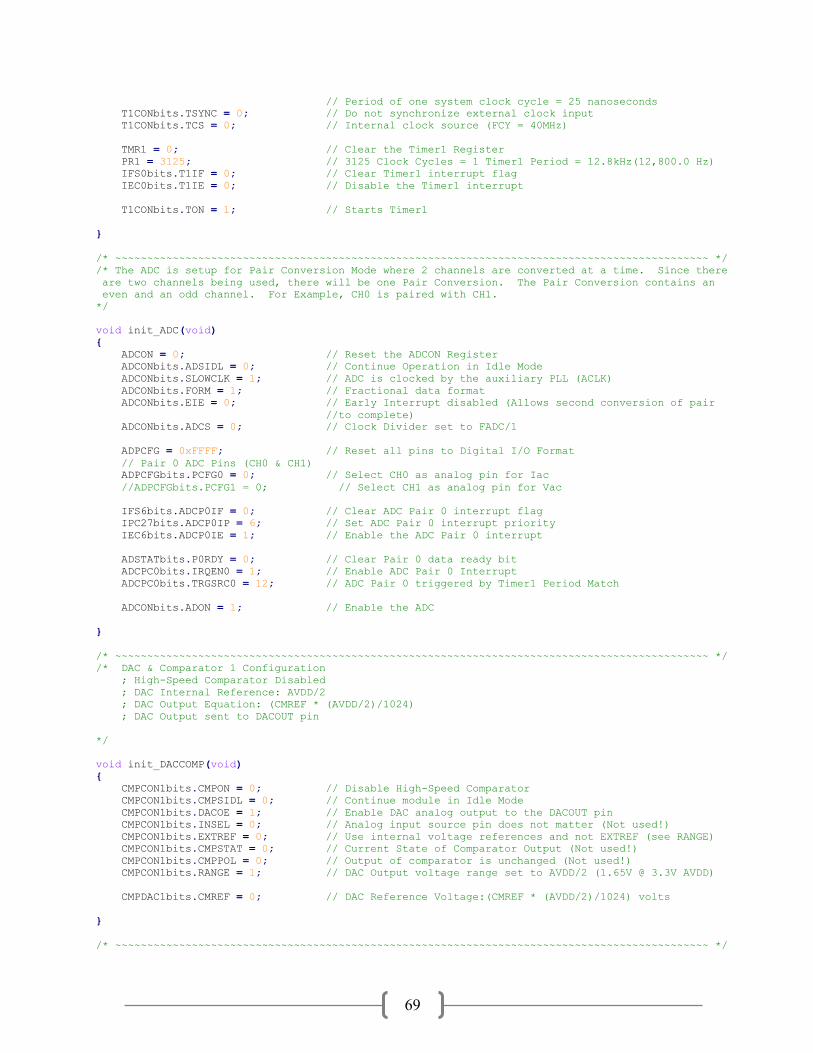
69
// Period of one system clock cycle = 25 nanoseconds
T1CONbits.TSYNC = 0; // Do not synchronize external clock input
T1CONbits.TCS = 0; // Internal clock source (FCY = 40MHz)
TMR1 = 0; // Clear the Timer1 Register
PR1 = 3125; // 3125 Clock Cycles = 1 Timer1 Period = 12.8kHz(12,800.0 Hz)
IFS0bits.T1IF = 0; // Clear Timer1 interrupt flag
IEC0bits.T1IE = 0; // Disable the Timer1 interrupt
T1CONbits.TON = 1; // Starts Timer1
}
/* ~~~~~~~~~~~~~~~~~~~~~~~~~~~~~~~~~~~~~~~~~~~~~~~~~~~~~~~~~~~~~~~~~~~~~~~~~~~~~~~~~~~~~~~~~~~~~ */
/* The ADC is setup for Pair Conversion Mode where 2 channels are converted at a time. Since there
are two channels being used, there will be one Pair Conversion. The Pair Conversion contains an
even and an odd channel. For Example, CH0 is paired with CH1.
*/
void init_ADC(void)
{
ADCON = 0; // Reset the ADCON Register
ADCONbits.ADSIDL = 0; // Continue Operation in Idle Mode
ADCONbits.SLOWCLK = 1; // ADC is clocked by the auxiliary PLL (ACLK)
ADCONbits.FORM = 1; // Fractional data format
ADCONbits.EIE = 0; // Early Interrupt disabled (Allows second conversion of pair
//to complete)
ADCONbits.ADCS = 0; // Clock Divider set to FADC/1
ADPCFG = 0xFFFF; // Reset all pins to Digital I/O Format
// Pair 0 ADC Pins (CH0 & CH1)
ADPCFGbits.PCFG0 = 0; // Select CH0 as analog pin for Iac
//ADPCFGbits.PCFG1 = 0; // Select CH1 as analog pin for Vac
IFS6bits.ADCP0IF = 0; // Clear ADC Pair 0 interrupt flag
IPC27bits.ADCP0IP = 6; // Set ADC Pair 0 interrupt priority
IEC6bits.ADCP0IE = 1; // Enable the ADC Pair 0 interrupt
ADSTATbits.P0RDY = 0; // Clear Pair 0 data ready bit
ADCPC0bits.IRQEN0 = 1; // Enable ADC Pair 0 Interrupt
ADCPC0bits.TRGSRC0 = 12; // ADC Pair 0 triggered by Timer1 Period Match
ADCONbits.ADON = 1; // Enable the ADC
}
/* ~~~~~~~~~~~~~~~~~~~~~~~~~~~~~~~~~~~~~~~~~~~~~~~~~~~~~~~~~~~~~~~~~~~~~~~~~~~~~~~~~~~~~~~~~~~~~ */
/* DAC & Comparator 1 Configuration
; High-Speed Comparator Disabled
; DAC Internal Reference: AVDD/2
; DAC Output Equation: (CMREF * (AVDD/2)/1024)
; DAC Output sent to DACOUT pin
*/
void init_DACCOMP(void)
{
CMPCON1bits.CMPON = 0; // Disable High-Speed Comparator
CMPCON1bits.CMPSIDL = 0; // Continue module in Idle Mode
CMPCON1bits.DACOE = 1; // Enable DAC analog output to the DACOUT pin
CMPCON1bits.INSEL = 0; // Analog input source pin does not matter (Not used!)
CMPCON1bits.EXTREF = 0; // Use internal voltage references and not EXTREF (see RANGE)
CMPCON1bits.CMPSTAT = 0; // Current State of Comparator Output (Not used!)
CMPCON1bits.CMPPOL = 0; // Output of comparator is unchanged (Not used!)
CMPCON1bits.RANGE = 1; // DAC Output voltage range set to AVDD/2 (1.65V @ 3.3V AVDD)
CMPDAC1bits.CMREF = 0; // DAC Reference Voltage:(CMREF * (AVDD/2)/1024) volts
}
/* ~~~~~~~~~~~~~~~~~~~~~~~~~~~~~~~~~~~~~~~~~~~~~~~~~~~~~~~~~~~~~~~~~~~~~~~~~~~~~~~~~~~~~~~~~~~~~ */
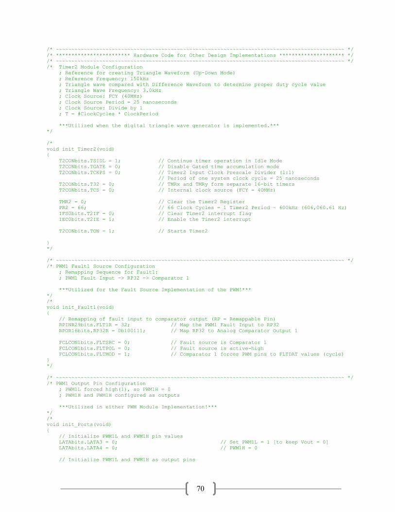
70
/* ~~~~~~~~~~~~~~~~~~~~~~~~~~~~~~~~~~~~~~~~~~~~~~~~~~~~~~~~~~~~~~~~~~~~~~~~~~~~~~~~~~~~~~~~~~~~~ */
/* ************************ Hardware Code for Other Design Implementations ********************* */
/* ~~~~~~~~~~~~~~~~~~~~~~~~~~~~~~~~~~~~~~~~~~~~~~~~~~~~~~~~~~~~~~~~~~~~~~~~~~~~~~~~~~~~~~~~~~~~~ */
/* Timer2 Module Configuration
; Reference for creating Triangle Waveform (Up-Down Mode)
; Reference Frequency: 150kHz
; Triangle wave compared with Difference Waveform to determine proper duty cycle value
; Triangle Wave Frequency: 3.0kHz
; Clock Source: FCY (40MHz)
; Clock Source Period = 25 nanoseconds
; Clock Source: Divide by 1
; T = #ClockCycles * ClockPeriod
***Utilized when the digital triangle wave generator is implemented.***
*/
/*
void init_Timer2(void)
{
T2CONbits.TSIDL = 1; // Continue timer operation in Idle Mode
T2CONbits.TGATE = 0; // Disable Gated time accumulation mode
T2CONbits.TCKPS = 0; // Timer2 Input Clock Prescale Divider (1:1)
// Period of one system clock cycle = 25 nanoseconds
T2CONbits.T32 = 0; // TMRx and TMRy form separate 16-bit timers
T2CONbits.TCS = 0; // Internal clock source (FCY = 40MHz)
TMR2 = 0; // Clear the Timer2 Register
PR2 = 66; // 66 Clock Cycles = 1 Timer2 Period ~ 600kHz (606,060.61 Hz)
IFS0bits.T2IF = 0; // Clear Timer2 interrupt flag
IEC0bits.T2IE = 1; // Enable the Timer2 interrupt
T2CONbits.TON = 1; // Starts Timer2
}
*/
/* ~~~~~~~~~~~~~~~~~~~~~~~~~~~~~~~~~~~~~~~~~~~~~~~~~~~~~~~~~~~~~~~~~~~~~~~~~~~~~~~~~~~~~~~~~~~~~ */
/* PWM1 Fault1 Source Configuration
; Remapping Sequence for Fault1:
; PWM1 Fault Input -> RP32 -> Comparator 1
***Utilized for the Fault Source Implementation of the PWM!***
*/
/*
void init_Fault1(void)
{
// Remapping of fault input to comparator output (RP = Remappable Pin)
RPINR29bits.FLT1R = 32; // Map the PWM1 Fault Input to RP32
RPOR16bits.RP32R = 0b100111; // Map RP32 to Analog Comparator Output 1
FCLCON1bits.FLTSRC = 0; // Fault source is Comparator 1
FCLCON1bits.FLTPOL = 0; // Fault source is active-high
FCLCON1bits.FLTMOD = 1; // Comparator 1 forces PWM pins to FLTDAT values (cycle)
}
*/
/* ~~~~~~~~~~~~~~~~~~~~~~~~~~~~~~~~~~~~~~~~~~~~~~~~~~~~~~~~~~~~~~~~~~~~~~~~~~~~~~~~~~~~~~~~~~~~~ */
/* PWM1 Output Pin Configuration
; PWM1L forced high(1), so PWM1H = 0
; PWM1H and PWM1H configured as outputs
***Utilized in either PWM Module Implementation!***
*/
/*
void init_Ports(void)
{
// Initialize PWM1L and PWM1H pin values
LATAbits.LATA3 = 0; // Set PWM1L = 1 [to keep Vout = 0]
LATAbits.LATA4 = 0; // PWM1H = 0
// Initialize PWM1L and PWM1H as output pins
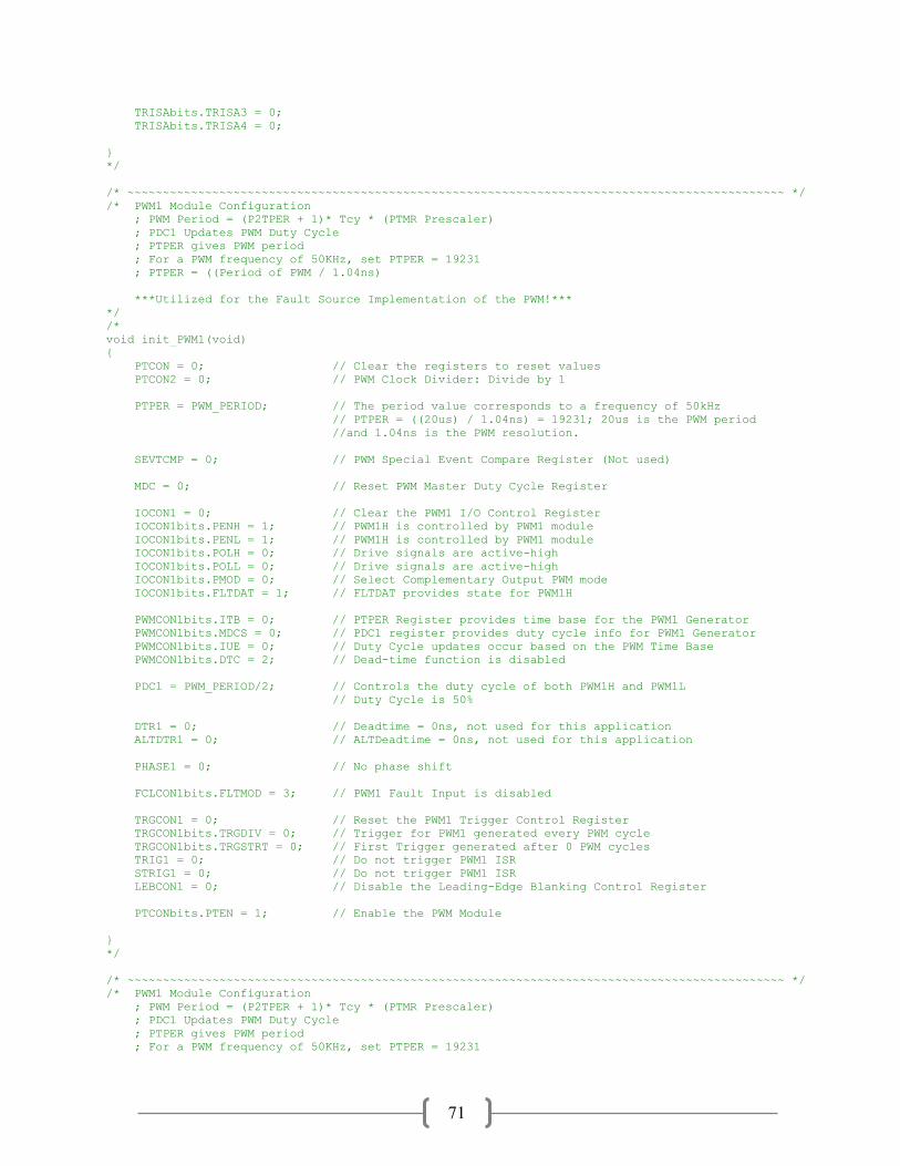
71
TRISAbits.TRISA3 = 0;
TRISAbits.TRISA4 = 0;
}
*/
/* ~~~~~~~~~~~~~~~~~~~~~~~~~~~~~~~~~~~~~~~~~~~~~~~~~~~~~~~~~~~~~~~~~~~~~~~~~~~~~~~~~~~~~~~~~~~~~ */
/* PWM1 Module Configuration
; PWM Period = (P2TPER + 1)* Tcy * (PTMR Prescaler)
; PDC1 Updates PWM Duty Cycle
; PTPER gives PWM period
; For a PWM frequency of 50KHz, set PTPER = 19231
; PTPER = ((Period of PWM / 1.04ns)
***Utilized for the Fault Source Implementation of the PWM!***
*/
/*
void init_PWM1(void)
{
PTCON = 0; // Clear the registers to reset values
PTCON2 = 0; // PWM Clock Divider: Divide by 1
PTPER = PWM_PERIOD; // The period value corresponds to a frequency of 50kHz
// PTPER = ((20us) / 1.04ns) = 19231; 20us is the PWM period
//and 1.04ns is the PWM resolution.
SEVTCMP = 0; // PWM Special Event Compare Register (Not used)
MDC = 0; // Reset PWM Master Duty Cycle Register
IOCON1 = 0; // Clear the PWM1 I/O Control Register
IOCON1bits.PENH = 1; // PWM1H is controlled by PWM1 module
IOCON1bits.PENL = 1; // PWM1H is controlled by PWM1 module
IOCON1bits.POLH = 0; // Drive signals are active-high
IOCON1bits.POLL = 0; // Drive signals are active-high
IOCON1bits.PMOD = 0; // Select Complementary Output PWM mode
IOCON1bits.FLTDAT = 1; // FLTDAT provides state for PWM1H
PWMCON1bits.ITB = 0; // PTPER Register provides time base for the PWM1 Generator
PWMCON1bits.MDCS = 0; // PDC1 register provides duty cycle info for PWM1 Generator
PWMCON1bits.IUE = 0; // Duty Cycle updates occur based on the PWM Time Base
PWMCON1bits.DTC = 2; // Dead-time function is disabled
PDC1 = PWM_PERIOD/2; // Controls the duty cycle of both PWM1H and PWM1L
// Duty Cycle is 50%
DTR1 = 0; // Deadtime = 0ns, not used for this application
ALTDTR1 = 0; // ALTDeadtime = 0ns, not used for this application
PHASE1 = 0; // No phase shift
FCLCON1bits.FLTMOD = 3; // PWM1 Fault Input is disabled
TRGCON1 = 0; // Reset the PWM1 Trigger Control Register
TRGCON1bits.TRGDIV = 0; // Trigger for PWM1 generated every PWM cycle
TRGCON1bits.TRGSTRT = 0; // First Trigger generated after 0 PWM cycles
TRIG1 = 0; // Do not trigger PWM1 ISR
STRIG1 = 0; // Do not trigger PWM1 ISR
LEBCON1 = 0; // Disable the Leading-Edge Blanking Control Register
PTCONbits.PTEN = 1; // Enable the PWM Module
}
*/
/* ~~~~~~~~~~~~~~~~~~~~~~~~~~~~~~~~~~~~~~~~~~~~~~~~~~~~~~~~~~~~~~~~~~~~~~~~~~~~~~~~~~~~~~~~~~~~~ */
/* PWM1 Module Configuration
; PWM Period = (P2TPER + 1)* Tcy * (PTMR Prescaler)
; PDC1 Updates PWM Duty Cycle
; PTPER gives PWM period
; For a PWM frequency of 50KHz, set PTPER = 19231
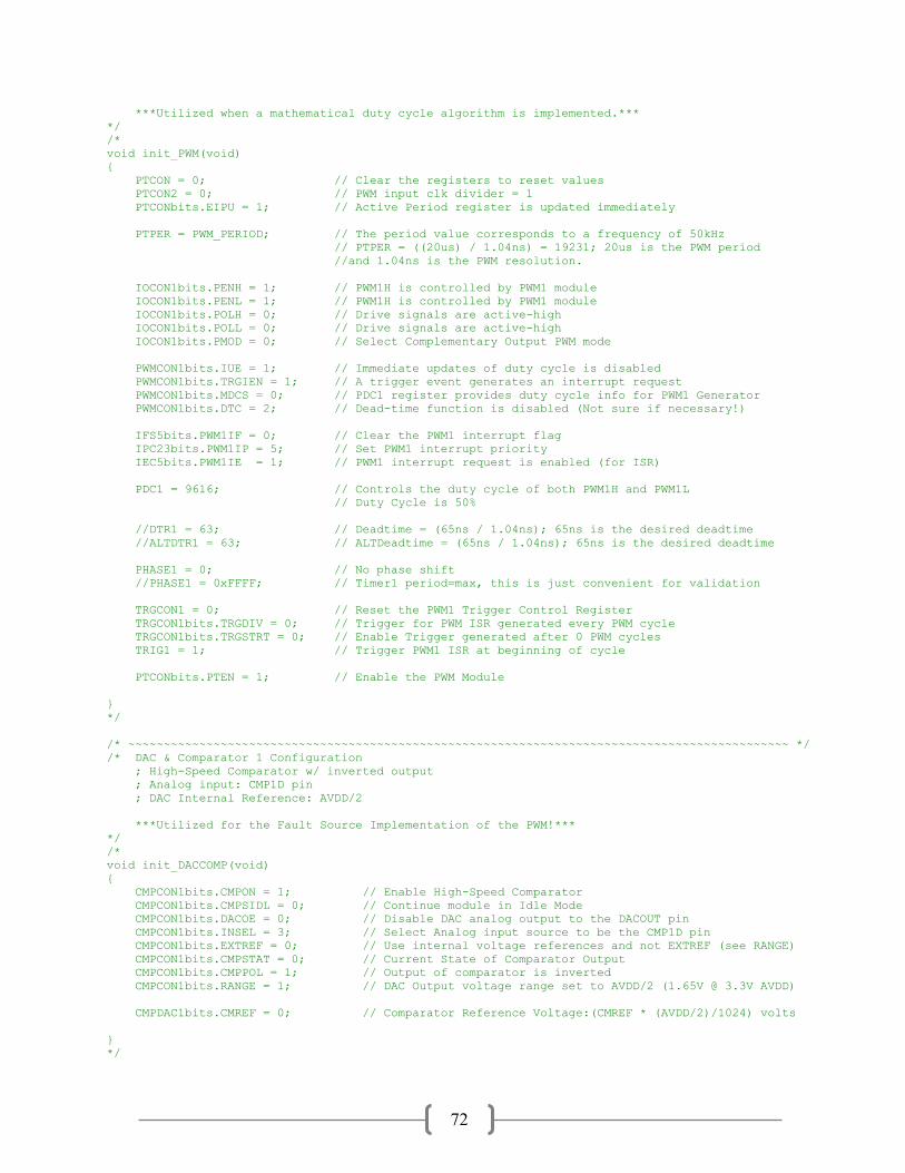
72
***Utilized when a mathematical duty cycle algorithm is implemented.***
*/
/*
void init_PWM(void)
{
PTCON = 0; // Clear the registers to reset values
PTCON2 = 0; // PWM input clk divider = 1
PTCONbits.EIPU = 1; // Active Period register is updated immediately
PTPER = PWM_PERIOD; // The period value corresponds to a frequency of 50kHz
// PTPER = ((20us) / 1.04ns) = 19231; 20us is the PWM period
//and 1.04ns is the PWM resolution.
IOCON1bits.PENH = 1; // PWM1H is controlled by PWM1 module
IOCON1bits.PENL = 1; // PWM1H is controlled by PWM1 module
IOCON1bits.POLH = 0; // Drive signals are active-high
IOCON1bits.POLL = 0; // Drive signals are active-high
IOCON1bits.PMOD = 0; // Select Complementary Output PWM mode
PWMCON1bits.IUE = 1; // Immediate updates of duty cycle is disabled
PWMCON1bits.TRGIEN = 1; // A trigger event generates an interrupt request
PWMCON1bits.MDCS = 0; // PDC1 register provides duty cycle info for PWM1 Generator
PWMCON1bits.DTC = 2; // Dead-time function is disabled (Not sure if necessary!)
IFS5bits.PWM1IF = 0; // Clear the PWM1 interrupt flag
IPC23bits.PWM1IP = 5; // Set PWM1 interrupt priority
IEC5bits.PWM1IE = 1; // PWM1 interrupt request is enabled (for ISR)
PDC1 = 9616; // Controls the duty cycle of both PWM1H and PWM1L
// Duty Cycle is 50%
//DTR1 = 63; // Deadtime = (65ns / 1.04ns); 65ns is the desired deadtime
//ALTDTR1 = 63; // ALTDeadtime = (65ns / 1.04ns); 65ns is the desired deadtime
PHASE1 = 0; // No phase shift
//PHASE1 = 0xFFFF; // Timer1 period=max, this is just convenient for validation
TRGCON1 = 0; // Reset the PWM1 Trigger Control Register
TRGCON1bits.TRGDIV = 0; // Trigger for PWM ISR generated every PWM cycle
TRGCON1bits.TRGSTRT = 0; // Enable Trigger generated after 0 PWM cycles
TRIG1 = 1; // Trigger PWM1 ISR at beginning of cycle
PTCONbits.PTEN = 1; // Enable the PWM Module
}
*/
/* ~~~~~~~~~~~~~~~~~~~~~~~~~~~~~~~~~~~~~~~~~~~~~~~~~~~~~~~~~~~~~~~~~~~~~~~~~~~~~~~~~~~~~~~~~~~~~ */
/* DAC & Comparator 1 Configuration
; High-Speed Comparator w/ inverted output
; Analog input: CMP1D pin
; DAC Internal Reference: AVDD/2
***Utilized for the Fault Source Implementation of the PWM!***
*/
/*
void init_DACCOMP(void)
{
CMPCON1bits.CMPON = 1; // Enable High-Speed Comparator
CMPCON1bits.CMPSIDL = 0; // Continue module in Idle Mode
CMPCON1bits.DACOE = 0; // Disable DAC analog output to the DACOUT pin
CMPCON1bits.INSEL = 3; // Select Analog input source to be the CMP1D pin
CMPCON1bits.EXTREF = 0; // Use internal voltage references and not EXTREF (see RANGE)
CMPCON1bits.CMPSTAT = 0; // Current State of Comparator Output
CMPCON1bits.CMPPOL = 1; // Output of comparator is inverted
CMPCON1bits.RANGE = 1; // DAC Output voltage range set to AVDD/2 (1.65V @ 3.3V AVDD)
CMPDAC1bits.CMREF = 0; // Comparator Reference Voltage:(CMREF * (AVDD/2)/1024) volts
}
*/
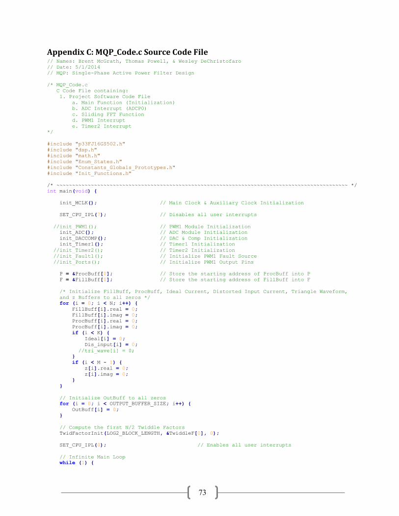
73
Appendix C: MQP_Code.c Source Code File // Names: Brent McGrath, Thomas Powell, & Wesley DeChristofaro
// Date: 5/1/2014
// MQP: Single-Phase Active Power Filter Design
/* MQP_Code.c
C Code File containing:
1. Project Software Code File
a. Main Function (Initialization)
b. ADC Interrupt (ADCP0)
c. Sliding FFT Function
d. PWM1 Interrupt
e. Timer2 Interrupt
*/
#include "p33FJ16GS502.h"
#include "dsp.h"
#include "math.h"
#include "Enum_States.h"
#include "Constants_Globals_Prototypes.h"
#include "Init_Functions.h"
/* ~~~~~~~~~~~~~~~~~~~~~~~~~~~~~~~~~~~~~~~~~~~~~~~~~~~~~~~~~~~~~~~~~~~~~~~~~~~~~~~~~~~~~~~~~~~~~ */
int main(void) {
init_MCLK(); // Main Clock & Auxiliary Clock Initialization
SET_CPU_IPL(7); // Disables all user interrupts
//init_PWM1(); // PWM1 Module Initialization
init_ADC(); // ADC Module Initialization
init_DACCOMP(); // DAC & Comp Initialization
init_Timer1(); // Timer1 Initialization
//init_Timer2(); // Timer2 Initialization
//init_Fault1(); // Initialize PWM1 Fault Source
//init_Ports(); // Initialize PWM1 Output Pins
P = &ProcBuff[0]; // Store the starting address of ProcBuff into P
F = &FillBuff[0]; // Store the starting address of FillBuff into F
/* Initialize FillBuff, ProcBuff, Ideal Current, Distorted Input Current, Triangle Waveform,
and z Buffers to all zeros */
for (i = 0; i < N; i++) {
FillBuff[i].real = 0;
FillBuff[i].imag = 0;
ProcBuff[i].real = 0;
ProcBuff[i].imag = 0;
if (i < K) {
Ideal[i] = 0;
Dis_input[i] = 0;
//tri_wave[i] = 0;
}
if (i < M - 1) {
z[i].real = 0;
z[i].imag = 0;
}
}
// Initialize OutBuff to all zeros
for (i = 0; i < OUTPUT_BUFFER_SIZE; i++) {
OutBuff[i] = 0;
}
// Compute the first N/2 Twiddle Factors
TwidFactorInit(LOG2_BLOCK_LENGTH, &TwiddleF[0], 0);
SET_CPU_IPL(0); // Enables all user interrupts
// Infinite Main Loop
while (1) {
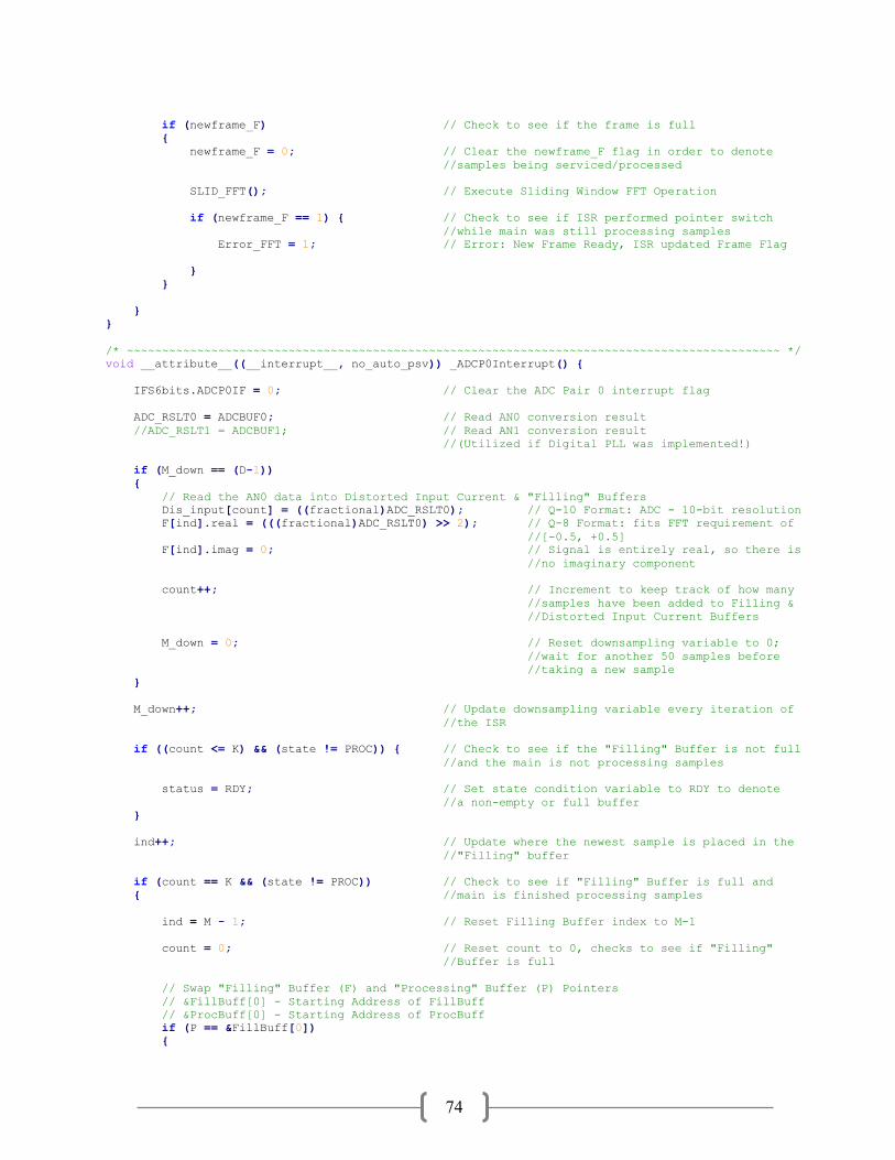
74
if (newframe_F) // Check to see if the frame is full
{
newframe_F = 0; // Clear the newframe_F flag in order to denote
//samples being serviced/processed
SLID_FFT(); // Execute Sliding Window FFT Operation
if (newframe_F == 1) { // Check to see if ISR performed pointer switch
//while main was still processing samples
Error_FFT = 1; // Error: New Frame Ready, ISR updated Frame Flag
}
}
}
}
/* ~~~~~~~~~~~~~~~~~~~~~~~~~~~~~~~~~~~~~~~~~~~~~~~~~~~~~~~~~~~~~~~~~~~~~~~~~~~~~~~~~~~~~~~~~~~~~ */
void __attribute__((__interrupt__, no_auto_psv)) _ADCP0Interrupt() {
IFS6bits.ADCP0IF = 0; // Clear the ADC Pair 0 interrupt flag
ADC_RSLT0 = ADCBUF0; // Read AN0 conversion result
//ADC_RSLT1 = ADCBUF1; // Read AN1 conversion result
//(Utilized if Digital PLL was implemented!)
if (M_down == (D-1))
{
// Read the AN0 data into Distorted Input Current & "Filling" Buffers
Dis_input[count] = ((fractional)ADC_RSLT0); // Q-10 Format: ADC - 10-bit resolution
F[ind].real = (((fractional)ADC_RSLT0) >> 2); // Q-8 Format: fits FFT requirement of
//[-0.5, +0.5]
F[ind].imag = 0; // Signal is entirely real, so there is
//no imaginary component
count++; // Increment to keep track of how many
//samples have been added to Filling &
//Distorted Input Current Buffers
M_down = 0; // Reset downsampling variable to 0;
//wait for another 50 samples before
//taking a new sample
}
M_down++; // Update downsampling variable every iteration of
//the ISR
if ((count <= K) && (state != PROC)) { // Check to see if the "Filling" Buffer is not full
//and the main is not processing samples
status = RDY; // Set state condition variable to RDY to denote
//a non-empty or full buffer
}
ind++; // Update where the newest sample is placed in the
//"Filling" buffer
if (count == K && (state != PROC)) // Check to see if "Filling" Buffer is full and
{ //main is finished processing samples
ind = M - 1; // Reset Filling Buffer index to M-1
count = 0; // Reset count to 0, checks to see if "Filling"
//Buffer is full
// Swap "Filling" Buffer (F) and "Processing" Buffer (P) Pointers
// &FillBuff[0] - Starting Address of FillBuff
// &ProcBuff[0] - Starting Address of ProcBuff
if (P == &FillBuff[0])
{
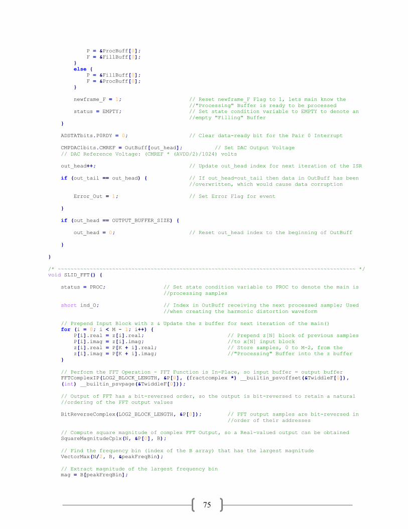
75
P = &ProcBuff[0];
F = &FillBuff[0];
}
else {
P = &FillBuff[0];
F = &ProcBuff[0];
}
newframe_F = 1; // Reset newframe_F Flag to 1, lets main know the
//"Processing" Buffer is ready to be processed
status = EMPTY; // Set state condition variable to EMPTY to denote an
//empty "Filling" Buffer
}
ADSTATbits.P0RDY = 0; // Clear data-ready bit for the Pair 0 Interrupt
CMPDAC1bits.CMREF = OutBuff[out_head]; // Set DAC Output Voltage
// DAC Reference Voltage: (CMREF * (AVDD/2)/1024) volts
out_head++; // Update out_head index for next iteration of the ISR
if (out_tail == out_head) { // If out_head=out_tail then data in OutBuff has been
//overwritten, which would cause data corruption
Error_Out = 1; // Set Error Flag for event
}
if (out_head == OUTPUT_BUFFER_SIZE) {
out_head = 0; // Reset out_head index to the beginning of OutBuff
}
}
/* ~~~~~~~~~~~~~~~~~~~~~~~~~~~~~~~~~~~~~~~~~~~~~~~~~~~~~~~~~~~~~~~~~~~~~~~~~~~~~~~~~~~~~~~~~~~~~ */
void SLID_FFT() {
status = PROC; // Set state condition variable to PROC to denote the main is
//processing samples
short ind_O; // Index in OutBuff receiving the next processed sample; Used
//when creating the harmonic distortion waveform
// Prepend Input Block with z & Update the z buffer for next iteration of the main()
for (i = 0; i < M - 1; i++) {
P[i].real = z[i].real; // Prepend z[N] block of previous samples
P[i].imag = z[i].imag; //to x[N] input block
z[i].real = P[K + i].real; // Store samples, 0 to M-2, from the
z[i].imag = P[K + i].imag; //"Processing" Buffer into the z buffer
}
// Perform the FFT Operation - FFT Function is In-Place, so input buffer = output buffer
FFTComplexIP(LOG2_BLOCK_LENGTH, &P[0], (fractcomplex *) __builtin_psvoffset(&TwiddleF[0]),
(int) __builtin_psvpage(&TwiddleF[0]));
// Output of FFT has a bit-reversed order, so the output is bit-reversed to retain a natural
//ordering of the FFT output values
BitReverseComplex(LOG2_BLOCK_LENGTH, &P[0]); // FFT output samples are bit-reversed in
//order of their addresses
// Compute square magnitude of complex FFT Output, so a Real-valued output can be obtained
SquareMagnitudeCplx(N, &P[0], B);
// Find the frequency bin (index of the B array) that has the largest magnitude
VectorMax(N/2, B, &peakFreqBin);
// Extract magnitude of the largest frequency bin
mag = B[peakFreqBin];

76
// Calculate phase of the largest frequency bin
theta = atan2(&P[peakFreqBin].imag, &P[peakFreqBin].real);
// Compute frequency (in Hz) of the largest spectral component
peakFreq = peakFreqBin*(DOWN_SAMPLING_RATE/N);
for (i = 0; i < K; i++) {
// Reconstruct the Ideal Current Waveform
Ideal[i] = ((mag*sin(peakFreq*2*PI*i + theta)) >> 6); // Q-10 Format: Magnitude is 16 bits
//and sin() ranges from [-1,1], so the
//Ideal Current needs to be shifted
//by 6 bits to be the same size as the
//Distorted Input Current
ind_O = out_tail + i; // Update index at which samples are
//placed into OutBuff
if(ind_O >= OUTPUT_BUFFER_SIZE) {
ind_O -= OUTPUT_BUFFER_SIZE; // Wrap ind_O index to the front of OutBuff
}
OutBuff[ind_O] = (unsigned short)((Ideal[i] - Dis_input[i])+2^10); //See Comment below:
// Subtraction of the Ideal Current and
//Distorted Input Current waveform isolates
//the *Harmonic Distortion waveform
//* The Harmonic Distortion waveform helps to
//derive the proper duty cycles for the PWM
//waveforms and when inverted models the ideal
//Compensation Current produced by the active
//power filter
}
out_tail += K; // Update where next sample is placed in OutBuff
//for next iteration of the Sliding FFT function
if(out_tail >= OUTPUT_BUFFER_SIZE) {
out_tail -= OUTPUT_BUFFER_SIZE; // Wrap out_tail to front of OutBuff
}
status = FIN; // Set state condition variable to FIN to denote
//completion of the processing critical section
}
/* ~~~~~~~~~~~~~~~~~~~~~~~~~~~~~~~~~~~~~~~~~~~~~~~~~~~~~~~~~~~~~~~~~~~~~~~~~~~~~~~~~~~~~~~~~~~~~ */
/*
// PWM1 Interrupt would be used if a mathematical duty cycle algorithm was implemented.
void __attribute__((__interrupt__, no_auto_psv)) _PWM1Interrupt() {
PWMCON1bits.TRGSTAT = 0; // No trigger interrupt is pending
IFS5bits.PWM1IF = 0; // Clear the PWM1 interrupt flag
// State system for determining the proper duty cycle value goes here
// ....
}
*/
/* ~~~~~~~~~~~~~~~~~~~~~~~~~~~~~~~~~~~~~~~~~~~~~~~~~~~~~~~~~~~~~~~~~~~~~~~~~~~~~~~~~~~~~~~~~~~~~ */
/*
// Frame-by-Frame Processing Version of Triangle Waveform Formation
void __attribute__((__interrupt__, no_auto_psv)) _T2Interrupt() {
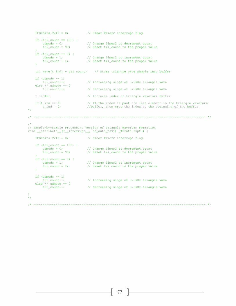
77
IFS0bits.T2IF = 0; // Clear Timer2 interrupt flag
if (tri_count == 100) {
udmode = 0; // Change Timer2 to decrement count
tri_count = 99; // Reset tri_count to the proper value
}
if (tri_count == 0) {
udmode = 1; // Change Timer2 to increment count
tri_count = 1; // Reset tri_count to the proper value
}
tri_wave[t_ind] = tri_count; // Store triangle wave sample into buffer
if (udmode == 1)
tri_count++; // Increasing slope of 3.0kHz triangle wave
else // udmode == 0
tri_count--; // Decreasing slope of 3.0kHz triangle wave
t_ind++; // Increase index of triangle waveform buffer
if(t_ind == K) // If the index is past the last element in the triangle waveform
t_ind = 0; //buffer, then wrap the index to the beginning of the buffer
*/
/* ~~~~~~~~~~~~~~~~~~~~~~~~~~~~~~~~~~~~~~~~~~~~~~~~~~~~~~~~~~~~~~~~~~~~~~~~~~~~~~~~~~~~~~~~~~~~~ */
/*
// Sample-by-Sample Processing Version of Triangle Waveform Formation
void __attribute__((__interrupt__, no_auto_psv)) _T2Interrupt() {
IFS0bits.T2IF = 0; // Clear Timer2 interrupt flag
if (tri_count == 100) {
udmode = 0; // Change Timer2 to decrement count
tri_count = 99; // Reset tri_count to the proper value
}
if (tri_count == 0) {
udmode = 1; // Change Timer2 to increment count
tri_count = 1; // Reset tri_count to the proper value
}
if (udmode == 1)
tri_count++; // Increasing slope of 3.0kHz triangle wave
else // udmode == 0
tri_count--; // Decreasing slope of 3.0kHz triangle wave
}
*/
/* ~~~~~~~~~~~~~~~~~~~~~~~~~~~~~~~~~~~~~~~~~~~~~~~~~~~~~~~~~~~~~~~~~~~~~~~~~~~~~~~~~~~~~~~~~~~~~ */
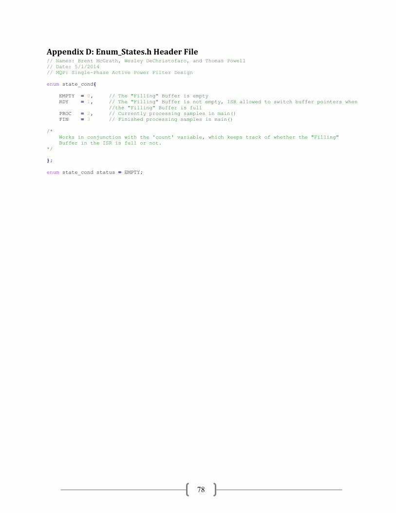
78
Appendix D: Enum_States.h Header File // Names: Brent McGrath, Wesley DeChristofaro, and Thomas Powell
// Date: 5/1/2014
// MQP: Single-Phase Active Power Filter Design
enum state_cond{
EMPTY = 0, // The "Filling" Buffer is empty
RDY = 1, // The "Filling" Buffer is not empty, ISR allowed to switch buffer pointers when
//the "Filling" Buffer is full
PROC = 2, // Currently processing samples in main()
FIN = 3 // Finished processing samples in main()
/*
Works in conjunction with the 'count' variable, which keeps track of whether the "Filling"
Buffer in the ISR is full or not.
*/
};
enum state_cond status = EMPTY;
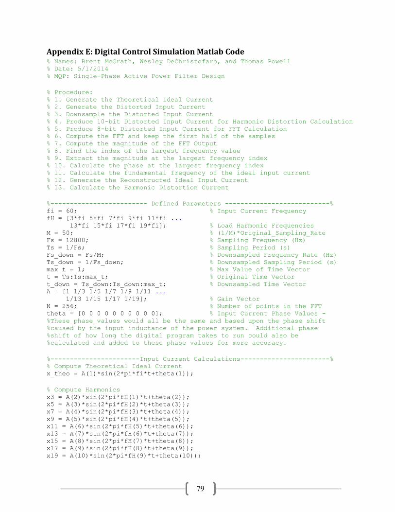
79
Appendix E: Digital Control Simulation Matlab Code % Names: Brent McGrath, Wesley DeChristofaro, and Thomas Powell % Date: 5/1/2014 % MQP: Single-Phase Active Power Filter Design
% Procedure: % 1. Generate the Theoretical Ideal Current % 2. Generate the Distorted Input Current % 3. Downsample the Distorted Input Current % 4. Produce 10-bit Distorted Input Current for Harmonic Distortion Calculation % 5. Produce 8-bit Distorted Input Current for FFT Calculation % 6. Compute the FFT and keep the first half of the samples % 7. Compute the magnitude of the FFT Output % 8. Find the index of the largest frequency value % 9. Extract the magnitude at the largest frequency index % 10. Calculate the phase at the largest frequency index % 11. Calculate the fundamental frequency of the ideal input current % 12. Generate the Reconstructed Ideal Input Current % 13. Calculate the Harmonic Distortion Current
%------------------------- Defined Parameters ---------------------------% fi = 60; % Input Current Frequency fH = [3*fi 5*fi 7*fi 9*fi 11*fi ... 13*fi 15*fi 17*fi 19*fi]; % Load Harmonic Frequencies M = 50; % (1/M)*Original_Sampling_Rate Fs = 12800; % Sampling Frequency (Hz) Ts = 1/Fs; % Sampling Period (s) Fs_down = Fs/M; % Downsampled Frequency Rate (Hz) Ts_down = 1/Fs_down; % Downsampled Sampling Period (s) max_t = 1; % Max Value of Time Vector t = Ts:Ts:max_t; % Original Time Vector t_down = Ts_down:Ts_down:max_t; % Downsampled Time Vector A = [1 1/3 1/5 1/7 1/9 1/11 ... 1/13 1/15 1/17 1/19]; % Gain Vector N = 256; % Number of points in the FFT theta = [0 0 0 0 0 0 0 0 0 0]; % Input Current Phase Values - %These phase values would all be the same and based upon the phase shift %caused by the input inductance of the power system. Additional phase %shift of how long the digital program takes to run could also be %calculated and added to these phase values for more accuracy.
%-----------------------Input Current Calculations-----------------------% % Compute Theoretical Ideal Current x_theo = A(1)*sin(2*pi*fi*t+theta(1));
% Compute Harmonics x3 = A(2)*sin(2*pi*fH(1)*t+theta(2)); x5 = A(3)*sin(2*pi*fH(2)*t+theta(3)); x7 = A(4)*sin(2*pi*fH(3)*t+theta(4)); x9 = A(5)*sin(2*pi*fH(4)*t+theta(5)); x11 = A(6)*sin(2*pi*fH(5)*t+theta(6)); x13 = A(7)*sin(2*pi*fH(6)*t+theta(7)); x15 = A(8)*sin(2*pi*fH(7)*t+theta(8)); x17 = A(9)*sin(2*pi*fH(8)*t+theta(9)); x19 = A(10)*sin(2*pi*fH(9)*t+theta(10));
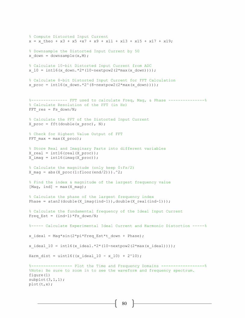
80
% Compute Distorted Input Current x = x_theo + x3 + x5 +x7 + x9 + x11 + x13 + x15 + x17 + x19;
% Downsample the Distorted Input Current by 50 x_down = downsample(x,M);
% Calculate 10-bit Distorted Input Current from ADC x_10 = int16(x_down.*2*(10-nextpow2(2*max(x_down))));
% Calculate 8-bit Distorted Input Current for FFT Calculation x_proc = int16(x_down.*2^(8-nextpow2(2*max(x_down))));
%--------------- FFT used to calculate Freq, Mag, & Phase ---------------% % Calculate Resolution of the FFT (in Hz) FFT_res = Fs_down/N;
% Calculate the FFT of the Distorted Input Current X_proc = fft(double(x_proc), N);
% Check for Highest Value Output of FFT FFT_max = max(X_proc);
% Store Real and Imaginary Parts into different variables X_real = int16(real(X_proc)); X_imag = int16(imag(X_proc));
% Calculate the magnitude (only keep 0:Fs/2) X_mag = abs(X_proc(1:floor(end/2))).^2;
% Find the index & magnitude of the largest frequency value [Mag, ind] = max(X_mag);
% Calculate the phase of the largest frequency index Phase = atan2(double(X_imag(ind-1)),double(X_real(ind-1)));
% Calculate the fundamental frequency of the Ideal Input Current Freq_Est = (ind-1)*Fs_down/N;
%----- Calculate Experimental Ideal Current and Harmonic Distortion -----%
x_ideal = Mag*sin(2*pi*Freq_Est*t_down + Phase);
x_ideal_10 = int16(x_ideal.*2*(10-nextpow2(2*max(x_ideal))));
Harm_dist = uint16((x_ideal_10 - x_10) + 2^10);
%----------------- Plot the Time and Frequency Domains ------------------% %Note: Be sure to zoom in to see the waveform and frequency spectrum. figure(1) subplot(3,1,1); plot(t,x);
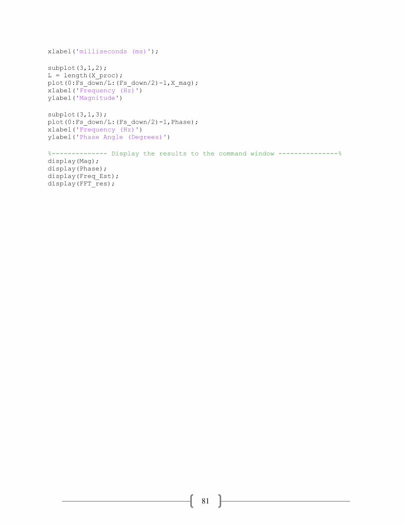
81
xlabel('milliseconds (ms)');
subplot(3,1,2); L = length(X_proc); plot(0:Fs_down/L:(Fs_down/2)-1,X_mag); xlabel('Frequency (Hz)') ylabel('Magnitude')
subplot(3,1,3); plot(0:Fs_down/L:(Fs_down/2)-1,Phase); xlabel('Frequency (Hz)') ylabel('Phase Angle (Degrees)')
%-------------- Display the results to the command window ---------------% display(Mag); display(Phase); display(Freq_Est); display(FFT_res);
[1-37]

82
References
[1] N. Mohan, T. M. Undeland, and W. P. Robbins, Power Electronics, Converters,
Applications and Design: John Wiley, 2003.
[2] Wikipedia. (2014). Harmonics (electrical power). Available: http://en.wikipedia.org/
[3] T. Blooming and D. Carnovale, "Application of IEEE Std 519-1992 Harmonic Limits," ed,
17 September 2007.
[4] H. Akagi, "Active Harmonic Filters," Proceedings of the IEEE, vol. 93, pp. 2128-2141,
December 2005.
[5] M. Thompson, Intuitive Analog Circuit Design, 2nd ed.: Elsevier Inc, 2014.
[6] IAMechatronics. Digitization of Analog Quantities.
[7] Wikipedia. (2014). Analog-to-digital converter. Available: http://en.wikipedia.org/
[8] P. Burk, L. Polanksy, D. Repetto, M. Roberts, and D. Rockmore, "Section 3.4: The DFT,
FFT, and IFFT," in Music and Computers A Theoretical and Historial Approach, ed.
[9] S. Long, "Phase Locked Loop Circuits," T. H. Lee, Ed., ed, 2005.
[10] M. Barr, "Introduction to Pulse Width Modulation (PWM)," Embedded Systems
Programming, pp. 103-104, September 2001.
[11] Protostack. (2011). ATmega168A Pulse Width Modulation - PWM.
[12] Wikipedia. (2014). Pulse-width modulation. Available: http://en.wikipedia.org/
[13] G. Terzulli and C. Hunter. (2007). Film Technology has Wind in its Sails.
[14] B. v. Oudtshoorn, "Music Transcription (Honours project)," ed, 2009.
[15] ON Semiconductor, "ADP3120A," in Dual Bootstrapped, 12 V MOSFET Driver with
Output Disable, ed, 2012, pp. 1, 4.
[16] D. R. Brown III, "Pre-Scaling to Avoid Overflow and Maintain Maximum Precision in
Fixed-Point Multiplication," ed, 2012, pp. 1-5.
[17] Microchip, "dsPIC33FJo6GS101/X02 and dsPIC33FJ16GSX02/X04," in 16-bit Digital
Signal Controllers (up to 16 KB Flash and up to 2 KB SRAM) with High-Speed PWM,
ADC, and Comparators, ed, 2012, pp. 135, 261.
[18] G. Lazaridis. (2009). Triangle Wave Generator.
[19] A. Andreas, "General Characteristics of Filters," in Passive, Active, and Digital Filters,
Second Edition, ed: CRC Press, 2009.
[20] A. Bhattacharya, C. Chakraborty, and S. Bhattacharya, "Shunt compensation," Industrial
Electronics Magazine, IEEE, vol. 3, pp. 38-49, 2009.
[21] B. K. Bose, Power Electronics and Motor Drives: Advances and Trends. Burlington, MA,
USA: Academic Press, 2006.
[22] Q. Chongming, K. M. Smedley, and F. Maddaleno, "A single-phase active power filter
with one-cycle control under unipolar operation," Circuits and Systems I: Regular Papers,
IEEE Transactions on, vol. 51, pp. 1623-1630, 2004.
[23] R. Costa-Castello, R. Grino, R. Cardoner Parpal, and E. Fossas, "High-Performance
Control of a Single-Phase Shunt Active Filter," Control Systems Technology, IEEE
Transactions on, vol. 17, pp. 1318-1329, 2009.
[24] R. Grino, R. Costa-Castello, and E. Fossas, "Digital control of a single-phase shunt active
filter," in Power Electronics Specialist Conference, 2003. PESC '03. 2003 IEEE 34th
Annual, 2003, pp. 1038-1042 vol.3.
[25] D. R. Kirtane, P. M. Sonwane, and B. E. Kushare, "Application of Active Power Filter for
Power Factor Correction of Nonlinear Loads," IOSR Journal of Engineering (IOSRJEN),
pp. 48-51, 2012.

83
[26] L. P. Kunjumuhammed and M. K. Mishra, "Comparison of single phase shunt active power
filter algorithms," in Power India Conference, 2006 IEEE, 2006, p. 8 pp.
[27] J.-H. Lee, J.-K. Jeong, B.-M. Han, and B.-Y. Bae, "New Reference Generation for a
Single-Phase Active Power Filter to Improve Steady State Performance," Journal of Power
Electronics, vol. 10, pp. 412-418, 4 July 2010.
[28] A. Martins, J. Ferreira, and H. Azevedo, "Active Power Filters for Harmonic Elimination
and Power Quality Improvement," in Power Quality, A. Eberhard, Ed., ed: InTech, 2011,
pp. 161-182.
[29] D. Martinsson and M. Lind, "DSP Controller for Power Electronic Converter
Applications," Industrial Eletrical Engineering and Automation, Lund University, 2006.
[30] F. Pottker de Souza and I. Barbi, "Single-phase active power filters for distributed power
factor correction," in Power Electronics Specialists Conference, 2000. PESC 00. 2000
IEEE 31st Annual, 2000, pp. 500-505 vol.1.
[31] S. Rahmani, K. Al-Haddad, and H. Y. Kanaan, "Two PWM techniques for single-phase
shunt active power filters employing a direct current control strategy," Power Electronics,
IET, vol. 1, pp. 376-385, 2008.
[32] M. H. Rashid, Power Electronics Handbook. San Diego, CA, USA: Academic Press, 2001.
[33] M. Rukonuzzaman and M. Nakaoka, "Single-phase shunt active power filter with novel
harmonic detection," in Power Electronics and Drive Systems, 2001. Proceedings., 2001
4th IEEE International Conference on, 2001, pp. 366-372 vol.1.
[34] B. Singh, K. Al-Haddad, and A. Chandra, "A review of active filters for power quality
improvement," Industrial Electronics, IEEE Transactions on, vol. 46, pp. 960-971, 1999.
[35] S. W. Smith, "Chapter 12: The Fast Fourier Transform," in The Scientist and Engineer's
Guide to Digital Signal Processing, ed. San Diego, CA, USA: California Technical
Publishing, 1997.
[36] K. P. Sozanski, "Improved shunt active power filters," in Nonsinusoidal Currents and
Compensation, 2008. ISNCC 2008. International School on, 2008, pp. 1-6.
[37] J. C. Wu and H. L. Jou, "Simplified control method for the single-phase active power
filter," Electric Power Applications, IEE Proceedings -, vol. 143, pp. 219-224, 1996.
Recommended