Copyright (c) 2011 IEEE. Personal use is permitted. For any other purposes, permission must be obtained from the IEEE by emailing [email protected].
This article has been accepted for publication in a future issue of this journal, but has not been fully edited. Content may change prior to final publication.
1
Abstract-- A novel high step-up converter is proposed for a front-end photovoltaic system. Through a
voltage multiplier module, an asymmetrical interleaved high step-up converter obtains high step-up gain
without operating at extreme duty ratio. The voltage multiplier module is composed of a conventional
boost converter and coupled inductors. An extra conventional boost converter is integrated into the first
phase to achieve a considerably higher voltage conversion ratio. The two-phase configuration not only
reduces the current stress through each power switch, but also constrains the input current ripple, which
decreases the conduction losses of MOSFETs. In addition, the proposed converter functions as an active
clamp circuit, which alleviates large voltage spikes across the power switches. Thus, the low-voltage-rated
MOSFETs can be adopted for reductions of conduction losses and cost. Efficiency improves because the
energy stored in leakage inductances is recycled to the output terminal. Finally, the prototype circuit with a
40- V input voltage, 380- V output, and 1000- W output power is operated to verify its performance. The
highest efficiency is 96.8%.
Index Terms-- Photovoltaic system, voltage multiplier module, boost-flyback converter, high step-up.
I. INTRODUCTION
ENEWABLE sources of energy are increasingly valued worldwide because of energy shortage and
environmental contamination. Renewable energy systems generate low voltage output; thus, high step-up
dc/dc converters are widely employed in many renewable energy applications, including fuel cells, wind
power, and photovoltaic systems [1]-[8]. Among renewable energy systems, photovoltaic systems are
expected to play an important role in future energy production [9]-[17]. Such systems transform light
K. C. Tseng, C. C. Huang, and W. Y. Shih
A High Step-Up Converter with Voltage
Multiplier Module for Photovoltaic System
R

Copyright (c) 2011 IEEE. Personal use is permitted. For any other purposes, permission must be obtained from the IEEE by emailing [email protected].
This article has been accepted for publication in a future issue of this journal, but has not been fully edited. Content may change prior to final publication.
2
energy into electrical energy, and convert low voltage into high voltage via a step-up converter, which can
convert energy into electricity using a grid-by-grid inverter or store energy into battery set. Fig. 1 shows a
typical photovoltaic system that consists of a solar module, a high step-up converter, a charge-discharge
controller, a battery set, and an inverter. The high step-up converter performs importantly among the
system because the system requires a sufficiently high step-up conversion.
Fig. 1. Typical photovoltaic system.
Theoretically, conventional step-up converters, such as the boost converter and flyback converter, cannot
achieve an high step-up conversion with high efficiency because of the resistances of elements or leakage
inductance. Thus, a modified boost-flyback converter was proposed [18]-[20], and many converters that
use the coupled inductor for a considerably high voltage conversion ratio were also proposed [21]-[25].
Despite these advances, conventional step-up converters with single-switch are unsuitable for high-
power applications given an input large current ripple, which increases conduction losses. Thus, numerous
interleaved structures and some asymmetrical interleaved structures are extensively used [26]-[33]. The
current study also presents an asymmetrical interleaved converter for high step-up and high-power
application.
Modifying a boost-flyback converter, shown in fig. 2(a), is one of the simple approaches to achieving
high step-up gain; this gain is realized via a coupled inductor. The performance of the converter is similar
to an active-clamped flyback converter; thus, the leakage energy is recovered to the output terminal [20].

Copyright (c) 2011 IEEE. Personal use is permitted. For any other purposes, permission must be obtained from the IEEE by emailing [email protected].
This article has been accepted for publication in a future issue of this journal, but has not been fully edited. Content may change prior to final publication.
3
An interleaved boost converter with a voltage-lift capacitor shown in fig. 2(b) is highly similar to the
conventional interleaved type. It obtains extra voltage gain through the voltage-lift capacitor, and reduces
the input current ripple, which is suitable for power factor correction (PFC) and high-power applications,
[34].
(a) (b)
Fig. 2. High step-up techniques based on classical boost converter. (a) Integrated flyback-boost converter structure. (b)
Interleaved boost converter with voltage-lift capacitor structure.
In this paper, an asymmetrical interleaved high step-up converter that combines the advantages of the
above-mentioned converters is proposed, which combined the advantages of both. In the voltage multiplier
module of the proposed converter, the turns ratio of coupled inductors can be designed to extend voltage
gain, and a voltage-lift capacitor offers an extra voltage conversion ratio.
The advantages of the proposed converter are as follows:
1) The converter is characterized by a low input current ripple and low conduction losses, making it
suitable for high-power applications.
2) The converter achieves the high step-up voltage gain that renewable energy systems require.
3) Leakage energy is recycled and sent to the output terminal, and alleviates large voltage spikes on the
main switch.

Copyright (c) 2011 IEEE. Personal use is permitted. For any other purposes, permission must be obtained from the IEEE by emailing [email protected].
This article has been accepted for publication in a future issue of this journal, but has not been fully edited. Content may change prior to final publication.
4
4) The main switch voltage stress of the converter is substantially lower than that of the output voltage.
5) Low cost and high efficiency are achieved by the low rDS(on) and low voltage rating of the power
switching device.
II. OPERATING PRINCIPLE DESCRIPTION
The proposed high step-up converter with voltage multiplier module is shown in Fig. 3(a). A
conventional boost converter and two coupled inductors are located in the voltage multiplier module,
which is stacked on a boost converter to form an asymmetrical interleaved structure.
(a) (b)
Fig. 3. (a) The proposed high step-up converter with voltage multiplier module. (b) Equivalent circuit of the proposed converter.
Primary windings of the coupled inductors with Np turns are employed to decrease input current ripple,
and secondary windings of the coupled inductors with Ns turns are connected in series to extend voltage
gain. The turns ratios of the coupled inductors are the same. The coupling references of the inductors are
denoted by „.‟ and „*‟ in Fig. 3.
The equivalent circuit of the proposed converter is shown in Fig. 3(b), where Lm1 and Lm2 are the
magnetizing inductors, Lk1 and Lk2 represent leakage inductors, S1 and S2 denote power switches, Cb is the

Copyright (c) 2011 IEEE. Personal use is permitted. For any other purposes, permission must be obtained from the IEEE by emailing [email protected].
This article has been accepted for publication in a future issue of this journal, but has not been fully edited. Content may change prior to final publication.
5
voltage-lift capacitor, and n is defined as turns ratio Ns/Np .
The proposed converter operates in continuous conduction mode (CCM), and the duty cycles of the
power switches during steady operation are interleaved with a 180-degree phase shift; the duty cycles are
greater than 0.5. The key steady waveforms in one switching period of the proposed converter contains six
modes, which are depicted in Fig. 4, and Fig. 5 shows the topological stages of the circuit.
Fig. 4. Steady waveforms of the proposed converter at CCM.
Mode 1 [to, t1]:
At t=t0, the power switches S1 and S2 are both turned on. All of the diodes are reversed-biased.

Copyright (c) 2011 IEEE. Personal use is permitted. For any other purposes, permission must be obtained from the IEEE by emailing [email protected].
This article has been accepted for publication in a future issue of this journal, but has not been fully edited. Content may change prior to final publication.
6
Magnetizing inductors Lm1 and Lm2, as well as leakage inductors Lk1 and Lk2, are linearly charged by input
voltage source Vin.
Mode 2 [t1, t2]:
At t=t1, power switch S2 is switched off, thereby turning on diodes D2 and D4. The energy that
magnetizing inductor Lm2 has stored is transferred to secondary side charging output filter capacitor C3. The
input voltage source, magnetizing inductor Lm2, leakage inductor Lk2, and voltage-lift capacitor Cb release
energy to output filter capacitor C1 via diode D2, thereby extending the voltage on C1.
Mode 3 [t2, t3]:
At t=t2, diode D2 automatically switches off because the total energy of leakage inductor Lk2 has been
completely released to output filter capacitor C1. Magnetizing inductor Lm2 transfers energy to secondary
side charging output filter capacitor C3 via diode D4 until t3.
Mode 4 [t3, t4]:
At t=t3, power switch S2 is switched on and all the diodes are turned off. The operating states of modes 1
and 4 are similar.
Mode 5 [t4, t5]:
At t=t4, power switch S1 is switched off, which turns on diodes D1 and D3. The energy stored in
magnetizing inductor Lm1 is transferred transfer to secondary side charging output filter capacitor C2. The
input voltage source and magnetizing inductor Lm1 release energy to voltage-lift capacitor Cb via diode D1,
which stores extra energy in Cb.
Mode 6 [t5, t0]:
At t=t5, diode D1 is automatically turned off because the total energy of leakage inductor Lk1 has been
completely released to voltage-lift capacitor Cb. Magnetizing inductor Lm1 transfers energy to secondary
side charging output filter capacitor C2 via diode D3 until t0.

Copyright (c) 2011 IEEE. Personal use is permitted. For any other purposes, permission must be obtained from the IEEE by emailing [email protected].
This article has been accepted for publication in a future issue of this journal, but has not been fully edited. Content may change prior to final publication.
7
(a) (b)
(c) (d)
(e) (f)
Fig. 5. Operating modes of the proposed converter. (a) Mode 1 [to, t1]. (b) Mode 2 [t1, t2]. (c) Mode 3 [t2, t3]. (d) Mode 4 [t3,
t4]. (e) Mode 5 [t4, t5]. (f) Mode 6 [t5, t0].

Copyright (c) 2011 IEEE. Personal use is permitted. For any other purposes, permission must be obtained from the IEEE by emailing [email protected].
This article has been accepted for publication in a future issue of this journal, but has not been fully edited. Content may change prior to final publication.
8
III. STEADY-STATE ANALYSIS
The transient characteristics of circuitry are disregarded to simplify the circuit performance analysis of
the proposed converter in CCM, and some formulated assumptions are as follows:
1) All of the components in the proposed converter are ideal.
2) Leakage inductors Lk1 and Lk2 are neglected.
3) Voltage VCb, VC1, VC2 and VC3 are considered to be constant because of infinitely large capacitance.
A. Voltage gain
The first phase converter can be regarded as a conventional boost converter; thus, voltage VCb can be
derived from
inCb V
DV
1
1 (1)
When switch S1 is turned on and switch S2 is turned off, voltage VC1 can be derived from
inCbinC V
DVV
DV
1
2
1
11
(2)
The output filter capacitors C2 and C3 are charged by energy transformation from the primary side. When
S2 is in turn-on state and S1 is in turn-off state, VC2 is equal to induced voltage of Ns1 plus induced voltage
of Ns2, and when S1 is in turn-on state and S2 is in turn-off state, VC3 is also equal to induced voltage of Ns1
plus induced voltage of Ns2. Thus, Voltages Vc2 and Vc3 can be derived from
2 3 (1 )1 1
C C in in
D nV V n V V
D D
(3)
The output voltage can be derived from
inCCCo V
D
nVVVV
1
22321
(4)
The voltage gain of the proposed converter is
D
n
V
V
in
o
1
22 (5)
Copyright (c) 2011 IEEE. Personal use is permitted. For any other purposes, permission must be obtained from the IEEE by emailing [email protected].
This article has been accepted for publication in a future issue of this journal, but has not been fully edited. Content may change prior to final publication.
9
Equation (5) confirms that the proposed converter has a high step-up voltage gain without an extreme
duty cycle. The curve of the voltage gain related to turns ratio n and duty cycle is shown in Fig. 6. When
the duty cycle is merely 0.6, the voltage gain reaches 10 at a turns ratio n of 1; the voltage gain reaches 30
at a turns ratio n of 5.
Fig. 6. The voltage gain versus turns ratio n and duty cycle.
B. Voltage stresses on semi-conductor components
The voltage ripples on the capacitors are ignored to simplify the voltage stress analyses of the
components of the proposed converter.
The voltage stresses on power switches S1 and S2 are derived from
1 2
1
1S S inV V V
D
(6)
The voltage stresses on the power switches S1 and S2 related to the output voltage Vo and the turns ratio n
can be expressed as
inoSS VD
nVVV
1
1221
(7)
Equations (6) and (7) confirm that low-voltage-rated MOSFETs with low RDS-ON can be adopted for the
proposed converter to reduce conduction losses and costs. This feature makes our converter suitable for
high step-up and high-power applications. The voltage stresses on the power switches account for half of
output voltage Vo, even if turns ratio n is 0.

Copyright (c) 2011 IEEE. Personal use is permitted. For any other purposes, permission must be obtained from the IEEE by emailing [email protected].
This article has been accepted for publication in a future issue of this journal, but has not been fully edited. Content may change prior to final publication.
10
The voltage stress on diode D1 is equal to VC1, and the voltage stress on diode D2 is voltage VC1 minus
voltage VCb. These voltage stresses can be derived from
inCD VD
VV
1
211
(8)
inCbCD V
DVVV
1
112
(9)
The voltage stresses on the diodes D1 and D2 related to the output voltage Vo and the turns ratio n can be
expressed as
inoD VD
nVV
1
21
(10)
inoD V
D
nVV
1
122
(11)
The voltage stresses on diodes D1 and D2 are close on power switches S1 and S2. Although the voltage
stress on diode D1 is larger, it accounts for only half of output voltage Vo at a turns ratio n one of 1. The
voltage stresses on the diodes are lower as the voltage gain is extended by increasing turns ratio n.
The voltage stresses on diodes D3 and D4 both equal the VC2 plus VC3, which can be derived from
inDD V
D
nVV
1
243
(12)
The voltage stresses on the diodes D3 and D4 related to the output voltage Vo and the turns ratio n can be
expressed as
inoDD VD
VVV
1
243
(13)
Although the voltage stresses on the diodes D3 and D4 increase as the turns ratio n increases, the voltage
stresses on the diodes D3 and D4 are always lower than the output voltage.
The relationship between the voltage stresses on all the semi-conductor components and the turns ratio n
is illustrated in Fig. 7.

Copyright (c) 2011 IEEE. Personal use is permitted. For any other purposes, permission must be obtained from the IEEE by emailing [email protected].
This article has been accepted for publication in a future issue of this journal, but has not been fully edited. Content may change prior to final publication.
11
Fig. 7. The voltage stresses on semi-conductor components versus turns ratio n.
C. Analysis of conduction losses
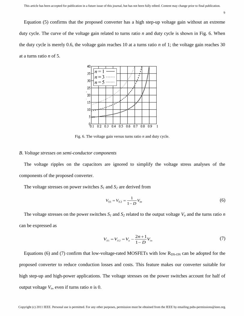
Some conduction losses are caused by resistances of semi-conductor components and coupled inductors.
Thus, all the components in the proposed converter are not assumed to be ideal, except for all the
capacitors. Diode reverse recovery problems, core losses, switching losses, and the ESR of capacitors are
not discussed in this section. The characteristics of leakage inductors are disregarded because of energy
recycling. The equivalent circuit, which includes the conduction losses of coupled inductors and semi-
conductor components, is shown in Fig. 8, in which rL11 and rL21 are the copper resistances of primary
windings of the coupled inductor; rL12 and rL22 are the copper resistances of secondary windings of the
coupled inductor; rDS1 and rDS2 denote the on-resistance of power switches; VD1, VD2, VD3, and VD4 denote
the forward biases of the diodes; and rD1, rD2, rD3, and rD4 are the resistances of the diodes.
Copyright (c) 2011 IEEE. Personal use is permitted. For any other purposes, permission must be obtained from the IEEE by emailing [email protected].
This article has been accepted for publication in a future issue of this journal, but has not been fully edited. Content may change prior to final publication.
12
Fig. 8. The equivalent circuit including conduction losses of coupled inductors and semi-conductor components.
Small-ripple approximation was used to calculate conduction losses. Thus, all currents that pass through
components were approximated by the DC components. The magnetizing currents and capacitor voltages
are assumed constant because of the infinite values of magnetizing inductors and capacitors. Fig. 9 shows
the PWM signals of S1 and S2. The equivalent operation states, including the four modes, are shown in Fig.
10.
Fig. 9. PWM signal of the S1 and S2.
Mode 1 [0, (D-0.5)]:
In this mode, power switches S1 and S2 are turned on, and diodes D1, D2, D3, and D4 are turned off. The
equivalent circuit is shown in Fig. 10(a), and the following equations can be derived:

Copyright (c) 2011 IEEE. Personal use is permitted. For any other purposes, permission must be obtained from the IEEE by emailing [email protected].
This article has been accepted for publication in a future issue of this journal, but has not been fully edited. Content may change prior to final publication.
13
11111 )( LmDSLLmin VrrIV
(14)
22212 )( LmDSLLmin VrrIV
(15)
Mode 2 [(D-0.5), 0.5]:
In this mode, power switch S2 is turned off, and diodes D2 and D4 are turned on. The equivalent circuit is
shown in Fig. 10(b), and the following equations can be derived:
111141 )()( LmDSLDLmin VrrnIIV
(16)
12
222142
)()(
CCbD
LmDLDLmin
VVV
VrrnIIV
(17)
4
422214213
)()(
D
DLLDLmLmC
V
rrrIVVnV
(18)
Mode 3 [0.5, D]:
This mode is similar to mode 1. The equivalent circuit is shown in Fig. 10(c), and the following equations
can be derived:
11111 )( LmDSLLmin VrrIV
(19)
22212 )( LmDSLLmin VrrIV
(20)
Mode 4 [D, 1]:
In this mode, power switch S1 is turned off, and diodes D1 and D3 are switched on. The equivalent circuit
is shown in Fig. 10(d), and the following equations can be derived:
221
22132
)(
)(
DSLmLm
LmLDLmin
rII
VrnIIV
(21)
CbDDSLmLm
LmDLDLmin
VVrII
VrrnIIV
1221
111131
)(
)()(
(22)
3
322213122
)()(
D
DLLDLmLmC
V
rrrIVVnV
(23)
The average currents that pass through diodes D1, D2, D3, and D4 can be derived by capacitor charge
balance.

Copyright (c) 2011 IEEE. Personal use is permitted. For any other purposes, permission must be obtained from the IEEE by emailing [email protected].
This article has been accepted for publication in a future issue of this journal, but has not been fully edited. Content may change prior to final publication.
14
In modes 1 and 3, both switches are turned off, and the average current that passes through output filter
capacitors C1, C2, and C3 are
o
oCCC
R
VIII 321
(24)
In mode 2, the average currents that pass through output filter capacitors C1 and C3 are
o
oDC
R
VII 21
(25)
o
oDC
R
VII 43
(26)
In mode 4, the average currents that pass through output filter capacitor C2 are as follows:
o
oDC
R
VII 32
(27)
The average currents that pass through diodes D2, D3, and D4 can be derived from
o
oDDD
RD
VIII
)1(432
(28)
In mode 2, ICb is equal to ID2; in mode 4, ICb is equal to the negative of ID1. Thus, the average current that
passes through diode D1 can be derived as follows:
o
oD
RD
VI
)1(1
(29)
In mode 4, the average value of ILm1 can be derived thus:
o
oDDLm
RD
VnnIII
)1(
)1(311
(30)
In mode 2, the average value of ILm2 can be derived by
o
oDDLm
RD
VnnIII
)1(
)1(422
(31)
The voltage conversion ratio with conduction losses can be derived from
)1(
])21[(
)1(
)12()1(1
)(1
1
22
2
2
2
4321
DR
rrn
DR
rDn
VVVVVD
n
V
V
o
YX
o
X
DDDD
in
in
o
(32)

Copyright (c) 2011 IEEE. Personal use is permitted. For any other purposes, permission must be obtained from the IEEE by emailing [email protected].
This article has been accepted for publication in a future issue of this journal, but has not been fully edited. Content may change prior to final publication.
15
where
22L21L12L11LX rrrrr
4321
2112222111
)(2
DDDD
DSDSLLLLY
rrrr
rrrrrrr
Because the turns ratio and copper resistances of the secondary windings of the coupled inductors are
directly proportional, the copper resistances of the coupled inductors can be expressed as
21221112 ; LLLL rnrrnr
Efficiency is expressed as follows:
)1(
])21[(
)1(
)12()1(1
)()22(
)1(1
2
2
2
4321
DR
rrn
DR
rDn
VVVVnV
D
o
YX
o
X
DDDD
in
(33)
(a) (b)

Copyright (c) 2011 IEEE. Personal use is permitted. For any other purposes, permission must be obtained from the IEEE by emailing [email protected].
This article has been accepted for publication in a future issue of this journal, but has not been fully edited. Content may change prior to final publication.
16
(c) (d)
Fig. 10. Equivalent operating modes with conduction losses states. (a) Mode 1 [0, (D-0.5)]. (b) Mode 2 [(D-0.5), 0.5]. (c) Mode
3 [0.5, D]. (d) Mode 4 [D, 1].
On the basis of (33), we infer that the efficiency will be higher if the input voltage is considerably higher
than the summation of the forward bias of all the diodes, or if the load is substantially larger than the
resistances of coupled inductors and semi-conductor components.
The calculated voltage gain and efficiency with different copper resistances are shown in Fig. 11, and
rL11 and rL21 is defined as rL. The other parameters in (33) are set as follows
1) Input voltage Vin : 40V
2) Turns ratio n :1
3) Load Ro : 200 ohm
4) On-resistances of switches rDS1 and rDS2 : 0.021ohm
5) Resistances of diodes rD1, rD2, rD3 and rD4 : 0.01ohm
6) Forward bias of diodes VD1, VD2, VD3 and VD4 : 1V
7) Copper resistances of secondary windings of coupled inductors rL12 and rL22 = rL at a turns ratio n of 1.
Fig. 11 reveals that efficiency and voltage gain are affected by the various coupled inductor winding
resistors and duty cycle, and that efficiency is decreased by the extreme duty ratio.

Copyright (c) 2011 IEEE. Personal use is permitted. For any other purposes, permission must be obtained from the IEEE by emailing [email protected].
This article has been accepted for publication in a future issue of this journal, but has not been fully edited. Content may change prior to final publication.
17
This chapter provides important information on voltage gain, voltage stresses on semi-conductor
components, and analysis of conduction losses, which indicates the relationship among duty cycle, turns
ratio, and components. The proposed converter for each application can be designed on the basis of
selected turns ratios, components, and other considerations.
Fig. 11. Calculated voltage gain and efficiency with different copper resistances.
D. performance comparison
For demonstrating the performance of proposed converter, the proposed converter is compared with
other high step-up interleaved converters introduced in [30], [33] as shown TABLE I.
The high step-up interleaved converter introduced in [30] is also suitable as a candidate for high step-up,
high power conversion of the PV system, and the other high step-up interleaved converter introduced in
[33], which is an asymmetrical interleaved structure as proposed converter, is favorable for DC-Microgrid
Copyright (c) 2011 IEEE. Personal use is permitted. For any other purposes, permission must be obtained from the IEEE by emailing [email protected].
This article has been accepted for publication in a future issue of this journal, but has not been fully edited. Content may change prior to final publication.
18
applications. Both of converters use coupled inductor and voltage-doubler to achieve high step-up
conversion.
TABLE I.
Performance conparison of interleaved high step-up converters
For the proposed converter, the step-up gain is highest and the voltage stress on switch is the lowest, as
converter introduced in [30]. Under the turns ratio n designed as less than 2, the highest voltage stress on
diodes of proposed converter is the lowest among the compared converters. In addition, the quantities of
diodes are the least as converter introduced in [33]. Because the components of proposed converter are the
least among the compared converters, the reliability is higher and the cost is lower. Thus, the proposed
converter is suitable for high step-up, high power applications such as PV system.

Copyright (c) 2011 IEEE. Personal use is permitted. For any other purposes, permission must be obtained from the IEEE by emailing [email protected].
This article has been accepted for publication in a future issue of this journal, but has not been fully edited. Content may change prior to final publication.
19
IV. DESIGN AND EXPERIMENT OF PROPOSED CONVERTER
A prototype of the proposed high step-up converter with a 40-V input voltage, 380-V output
voltage, and maximum output power of 1 kW is tested. The switching frequency is 40 kHz, and the
corresponding component parameters are listed in Table II for reference.
TABLE II
Converter components and parameters
The design consideration of the proposed converter includes components selection and coupled
inductors design, which are based on the analysis presented in the previous chapter. In the proposed
converter, the values of the primary leakage inductors of the coupled inductors are set as close as
possible for current sharing performance. Due to the performances of high step-up gain, the turns
ratio n can be set 1 for the prototype circuit with a 40- V input voltage, 380- V output to reduce cost,
volume and conduction loss of winding. Thus, the copper resistances which affect efficiency much
can be decreased.
The value of magnetizing inductors Lm1 and Lm2 can be design based on equation of boundary
operating condition, which is derived from
2
( )
(1 )
2( 1)(2 2)
om critical
s
D D RL
n n f
(34)
Where Lm(critical) is the value of magnetizing inductors at boundary operating condition, fs is the
switching frequency, and Ro is load. How to suppress the voltage ripple on the voltage-lift capacitor

Copyright (c) 2011 IEEE. Personal use is permitted. For any other purposes, permission must be obtained from the IEEE by emailing [email protected].
This article has been accepted for publication in a future issue of this journal, but has not been fully edited. Content may change prior to final publication.
20
Cb to an acceptable value is the main consideration. The equation versus the voltage ripple and the
output power or output current can be derived by
o ob
o s Cb s Cb
P IC
V f V f V
(35)
Where Po is the output power, Vo is the output voltage, fs is the switching frequency, and △VCb is
the voltage ripple on the voltage-lift capacitor Cb.
Fig. 12. Control strategy for the proposed converter.
In control strategy of proposed converter is implemented by microchip dsPIC30F4011 as shown
in Fig. 12. PV module and battery set are the main input power source, which can be seen as an
equivalent voltage source for the proposed converter, and the MPPT algorithm is employed by
referring [35]. The battery management system (BMS) for Charge/Discharge controller is not the
main priority in this paper thus the related designed is not implemented in the paper.
The output voltage is changed as load shift and the detected feedback signal is processed via
proportional-integral (PI) controller, and the internal comparator generates interleaved PWM with a

Copyright (c) 2011 IEEE. Personal use is permitted. For any other purposes, permission must be obtained from the IEEE by emailing [email protected].
This article has been accepted for publication in a future issue of this journal, but has not been fully edited. Content may change prior to final publication.
21
180-degree phase shift. Due to the insufficient voltage of PWM, the PWM are supported by
TC4420 to control power switches, and EL50P1 is a hall sensor to detect the input current for over-
current protection (OCP). The input voltage Vi supplied by PV module and battery set is very nearly
40 V even if the load shift. Thus, the efficiency of the proposed converter under constant input
voltage/constant output voltage can be measured.
(a) (b)
(c) (d)
Fig. 13. Measured waveform at Po=1 kW. (a)Vgs1, Vgs2, iLk1 and iLk2. (b)Vds1, Vds2 and iLs. (c) Vgs1, Vgs2, iD1 and iD2. (d) Vgs1,
Vgs2 , iD1 and iD2.
Fig. 13 illustrates the measured waveforms of Vgs1, Vgs2, iLk1, iLk2, Vds1, Vds2 and iLs at Po = 1kW. In
Fig. 13(b), the switch voltage is clamped at 90 V, which is much smaller than the output voltage
380V. Figs. 13(c) and 13(d) illustrates the measured waveforms of Vgs1, Vgs2, iD1, iD2, iD3 and iD4 at
Po = 1 kW. The measured waveforms are consistent with the steady-state analysis.
Copyright (c) 2011 IEEE. Personal use is permitted. For any other purposes, permission must be obtained from the IEEE by emailing [email protected].
This article has been accepted for publication in a future issue of this journal, but has not been fully edited. Content may change prior to final publication.
22
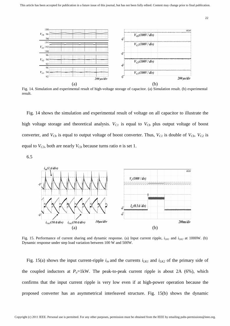
(a) (b)
Fig. 14. Simulation and experimental result of high-voltage storage of capacitor. (a) Simulation result. (b) experimental
result.
Fig. 14 shows the simulation and experimental result of voltage on all capacitor to illustrate the
high voltage storage and theoretical analysis. VC1 is equal to VCb plus output voltage of boost
converter, and VCb is equal to output voltage of boost converter. Thus, VC1 is double of VCb. VC2 is
equal to VC3, both are nearly VCb because turns ratio n is set 1.
6.5
(a) (b)
Fig. 15. Performance of current sharing and dynamic response. (a) Input current ripple, iLK1 and iLK2 at 1000W. (b)
Dynamic response under step load variation between 100 W and 500W.
Fig. 15(a) shows the input current-ripple iin and the currents iLK1 and iLK2 of the primary side of
the coupled inductors at Po=1kW. The peak-to-peak current ripple is about 2A (6%), which
confirms that the input current ripple is very low even if at high-power operation because the
proposed converter has an asymmetrical interleaved structure. Fig. 15(b) shows the dynamic

Copyright (c) 2011 IEEE. Personal use is permitted. For any other purposes, permission must be obtained from the IEEE by emailing [email protected].
This article has been accepted for publication in a future issue of this journal, but has not been fully edited. Content may change prior to final publication.
23
response due to the step load variation between 100 W and 500 W, and the output voltage is 380 V.
Fig. 16. Measured efficiency of proposed converter.
Fig. 17. Prototype photo of the proposed converter.
Fig. 16 shows the measured efficiency of the proposed converter. The maximum efficiency is
96.8% at PO = 400W. At maximum output power, the conversion efficiency is about 96.1%. Fig. 17
shows the prototype photo of the proposed converter.
V. CONCLUSION
This paper has presented the topological principles, steady-state analysis and experimental
results for a proposed converter. The proposed converter has been successfully implemented an
efficiently high step-up conversion without an extreme duty ratio and a number of turns ratios
through the voltage multiplier module and voltage clamp feature. The interleaved PWM scheme

Copyright (c) 2011 IEEE. Personal use is permitted. For any other purposes, permission must be obtained from the IEEE by emailing [email protected].
This article has been accepted for publication in a future issue of this journal, but has not been fully edited. Content may change prior to final publication.
24
reduces the currents that pass through each power switch and constrained the input current ripple by
approximately 6%. The experimental results indicate that leakage energy is recycled through
capacitor Cb to the output terminal. Meanwhile, the voltage stresses over the power switches are
restricted and are much lower than the output voltage (380 V). These switches, conducted to low
voltage rated and low on-state resistance MOSFET, can be selected. Furthermore, the full-load
efficiency is 96.1% at Po =1000 W, and the highest efficiency is 96.8% at Po = 400 W. Thus, the
proposed converter is suitable for PV systems or other renewable energy applications that need high
step-up high-power energy conversion.
References
[1] C. Hua, J. Lin, and C. Shen, “Implementation of a DSP-controlled photovoltaic system with
peak power tracking,” IEEE Trans. Ind. Electron., vol. 45, no. 1, pp. 99–107, Feb. 1998.
[2] J. M. Carrasco, L. G. Franquelo, J. T. Bialasiewicz, E. Galvan, R. C. P. Guisado, M. A. M Prats,
J. I. Leon, and N. Moreno-Alfonso, “Power-electronic systems for the grid integration of
renewable energy sources: A survey,” IEEE Trans. Ind. Electron., vol. 53, no. 4, pp. 1002–
1016, Jun. 2006.
[3] J. T. Bialasiewicz, “Renewable energy systems with photovoltaic power generators: Operation
and modeling,” IEEE Trans. Ind. Electron., vol. 55, no. 7, pp. 2752–2758, Jul. 2008.
[4] Y. Xiong, X. Cheng, Z. J. Shen, C. Mi, H. Wu, and V. K. Garg, “Prognostic and warning system
for power-electronic modules in electric, hybrid electric, and fuel-cell vehicles,” IEEE Trans.
Ind. Electron., vol. 55, no. 6, pp. 2268–2276, Jun. 2008.
[5] F. S. Pai, “An improved utility interface for micro-turbine generation system with stand-alone
operation capabilities,” IEEE Trans. Ind. Electron., vol. 53, no. 5, pp. 1529–1537, Oct. 2006.
[6] H. Tao, J. L. Duarte, and M. A.M. Hendrix, “Line-interactive UPS using a fuel cell as the
primary source,” IEEE Trans. Ind. Electron., vol. 55, no. 8, pp. 3012–3021, Aug. 2008.
Copyright (c) 2011 IEEE. Personal use is permitted. For any other purposes, permission must be obtained from the IEEE by emailing [email protected].
This article has been accepted for publication in a future issue of this journal, but has not been fully edited. Content may change prior to final publication.
25
[7] Z. Jiang and R. A. Dougal, “A compact digitally controlled fuel cell/battery hybrid power
source,” IEEE Trans. Ind. Electron., vol. 53, no. 4, pp. 1094–1104, Jun. 2006.
[8] Andersen, G.K., Klumpner, C., Kjaer, S.B., and Blaabjerg, F. “A new green power inverter for
fuel cells,” IEEE Power Electronics Specialists Conf., 2002, pp. 727–733
[9] Ghoddami, H. and Yazdani, A. “A single-stage three-phase photovoltaic system with enhanced
maximum power point tracking capability and increased power rating” IEEE Trans. Power
Del., vol. 26, no. 2, pp. 1017–1029, Apr. 2011.
[10] B. Yang, W. Li, Y. Zhao, and X. He, “Design and analysis of a grid-connected photovoltaic
power system,” IEEE Trans. Power Electron., vol. 25, no. 4, pp. 992–1000, Apr. 2010.
[11] W. Li, and X. He,“Review of Nonisolated high-step-up DC/DC converters in photovoltaic
grid-connected applications,” IEEE Trans. Ind. Electron., vol. 58, no. 4, pp. 1239–1250, Apr.
2011.
[12] A. I. Bratcu, I. Munteanu, S. Bacha, D. Picault, and B. Raison, “Cascaded dc–dc converter
photovoltaic systems: Power optimization issues,” IEEE Trans. Ind. Electron., vol. 58, no. 2,
pp. 403–411, Feb. 2011.
[13] R. J. Wai, W. H. Wang, and C. Y. Lin, “High-performance stand-alone photovoltaic generation
system,” IEEE Trans. Ind. Electron., vol. 55, no. 1, pp. 240–250, Jan. 2008.
[14] R. J. Wai and W. H. Wang, “Grid-connected photovoltaic generation system,” IEEE Trans.
Circuits Syst. I, Reg. Papers, vol. 55, no. 3, pp. 953–964, Apr. 2008.
[15] L. Gao, R. A. Dougal, S. Liu, and A. P. Iotova, “Parallel-connected solar PV system to address
partial and rapidly fluctuating shadow conditions,” IEEE Trans. Ind. Electron., vol. 56, no. 5,
pp. 1548–1556, May 2009.
[16] G. R. Walker and P. C. Sernia, “Cascaded DC–DC converter connection of photovoltaic
modules,” IEEE Trans. Power Electron., vol. 19, no. 4, pp. 1130–1139, Jul. 2004.
[17] K. Ujiie, T. Izumi, T. Yokoyama, and T. Haneyoshi, “Study on dynamic and static
Copyright (c) 2011 IEEE. Personal use is permitted. For any other purposes, permission must be obtained from the IEEE by emailing [email protected].
This article has been accepted for publication in a future issue of this journal, but has not been fully edited. Content may change prior to final publication.
26
characteristics of photovoltaic cell,” in Proc. Power Convers. Conf., Apr. 2–5, 2002, vol. 2, pp.
810–815.
[18] K. C. Tseng and T. J. Liang, “Novel high-efficiency step-up converter,” in Proc. Inst. Elect.
Eng.-Electr. Power Appl., vol. 151, no. 2, pp. 182–190, Mar. 2004.
[19] T. J. Liang and K. C. Tseng “Analysis of integrated boost-flyback step-up converter,” in Proc.
IEE-Elect. Power Applicat., vol. 152, no. 2, pp. 217–225, Mar. 2005.
[20] J. W. Baek, M. H. Ryoo, T. J. Kim, D. W. Yoo, J. S. Kim, “High boost converter using voltage
multiplier,” IEEE IECON, pp. 567-572,May. 2005.
[21] R. J. Wai and R. Y. Duan, “High step-up converter with coupled-inductor,” IEEE Trans. Power
Electron., vol. 20, no. 5, pp. 1025–1035, Sep. 2005.
[22] R. J. Wai, C. Y. Lin, R. Y. Duan, and Y. R. Chang, “High-efficiency DC–DC converter with
high voltage gain and reduced switch stress,” IEEE Trans. Ind. Electron., vol. 54, no. 1, pp.
354–364, Feb. 2007.
[23] S. K. Changchien, T. J. Liang, J. F. Chen, L. S. Yang, “Novel high step-up DC-DC converter
for fuel cell energy conversion system,” IEEE Trans. Ind. Electron., vol. 57, no. 6, pp. 2007-
2017, Jun. 2010.
[24] Y. P. Hsieh, J. F. Chen, T. J. Liang, L. S. Yang, “Novel high step-up dc–dc converter with
coupled-inductor and switched-capacitor techniques for a sustainable energy system,” IEEE
Trans. Power Electronics., vol. 26, no. 12, pp. 3481-3490, Dec. 2011.
[25] S. M. Chen, T. J. Liang; L. S. Yang; J. F. Chen, “A safety enhanced, high step-up dc-dc
converter for ac photovoltaic module application,” IEEE Trans. Power Electron., vol. 27, no. 4,
pp.1809-1817, Apr. 2012.
[26] W. Li, and X. He,“An interleaved winding-coupled boost converter with passive lossless
clamp circuits, ” IEEE Trans. Power Electron., vol. 22, no. 4, pp. 1499–1507, Jul. 2007.
[27] W. Li, and X. He,“A family of isolated interleaved boost and buck converters with winding-
Copyright (c) 2011 IEEE. Personal use is permitted. For any other purposes, permission must be obtained from the IEEE by emailing [email protected].
This article has been accepted for publication in a future issue of this journal, but has not been fully edited. Content may change prior to final publication.
27
cross-coupled inductors,” IEEE Trans. Power Electron., vol. 23, no. 6, pp. 3164–3173, Nov.
2008.
[28] D. Wang, X. He and J. Shi, “Design and analysis of an interleaved flyback–forward boost
converter with the current autobalance characteristic,” IEEE Trans. Power Electron., vol. 25,
no. 2, pp. 489–498, Feb. 2010.
[29] W. Li, Y. Zhao, Y. Deng, and X. He, “Interleaved converter with voltage multiplier cell for
high step-up and high-efficiency conversion,” IEEE Trans. Power Electron., vol. 25, no. 9, pp.
2397–2408, Sep. 2010.
[30] W. Li, Y. Zhao, J. Wu, and X. He, “Interleaved high step-up converter with winding-cross-
coupled inductors and voltage multiplier cells,” IEEE Trans. Power Electron., vol. 27, no. 1,
pp. 133–143, Jan. 2012.
[31] W. Li, W. Li, X. He, D. Xu, and B. Wu, “General derivation law of nonisolated high-step-up
interleaved converters with built-in transformer,” IEEE Trans. Ind. Electron., vol. 59, no. 3, pp.
1650–1661, Mar. 2012.
[32] C. T. Pan, C. M. Lai, “A high-efficiency high step-up converter with low switch voltage stress
for fuel-cell system applications,” IEEE Trans. Ind. Electron., vol. 57, no. 6, pp. 1998–2006,
Jun. 2010.
[33] C. M. Lai, C. T. Pan, M. C. Cheng, “High-efficiency modular high step-up interleaved boost
converter for DC-microgrid applications,” IEEE Trans. Ind. Electron., vol. 48, no. 1, pp. 161–
171, Jan/Feb. 2012.
[34] Y. T. Jang and M. M. Jovanovic, “Interleaved boost converter with intrinsic voltage-doubler
characteristic for universal-line PFC front end,” IEEE Trans. Power Electron., vol. 22, no. 4,
pp. 1394-1401, Jul. 2007.
[35] N. Femia, G. Petrone, G. Spagnuolo, and M. Vitelli, “Optimization of perturb and observe
maximum power point tracking method,” IEEE Trans. Power Electron., vol. 20, no. 4, pp.

Copyright (c) 2011 IEEE. Personal use is permitted. For any other purposes, permission must be obtained from the IEEE by emailing [email protected].
This article has been accepted for publication in a future issue of this journal, but has not been fully edited. Content may change prior to final publication.
28
963-973, Jul. 2005.
Recommended