A Flexible, Technology Adaptive
Memory Generation Tool
Adam C. Cabe, Zhenyu Qi, Wei Huang, Yan Zhang, Mircea R. Stan
(acc9x, zq7w, wh6p, yz3w, mircea)@virginia.edu
University of Virginia
Garrett S. Rose
Polytechnic University
Abstract
Memories are by far the most dominating circuit structure found in modern day application specific
integrated circuits (ASIC) and system-on-chips (SoC). When considering efficiency, it is not deemed good
practice to create different memories from scratch for every unique ASIC. In an era where technology is
ever improving and constantly changing, there is a need for versatile and technology adaptive memory
generators. There are innumerable types of memory designs; in industry, large teams are often devoted to
elaborate custom memory designs. This is generally not possible in academia, as resources and funds are
limited, and tight deadlines push for simpler, scalable and customizable memory architectures.
This session discusses a design flow methodology for developing a memory generator capable of handling
different memory designs and scaling across technology nodes. A highly automated flow, utilizing the
power of Cadence SKILL scripting, allows for smaller teams to generate dense and efficient memory
designs, as would be useful in academia. A generator is introduced for an IBM .18um technology,
developed in 4 to 6 weeks, and is capable of being ported to different technologies by simply changing
some technology specific parameters in the scripting. Participants will learn how to incorporate their
custom tailored circuits into this automated design flow, making this tool highly customizable. Additionally
they will learn to use Cadence Abstract Generator and RTL Compiler to incorporate this memory into a
synthesized design flow using Cadence Encounter. This methodology elicits a fast time-to-fabrication,
customizable, reproducible and affordable solution for memory generation.

I. Introduction
In modern day VLSI designs, memories are often the most dominating circuit structure found on the die.
This largely results from designs like systems on a chip (SoC), networks on a chip (NoC), and ultra-high
performance processors, which require large amounts of onboard memory. It is not deemed good practice
to design each memory from scratch for every unique application specific integrated circuit (ASIC). In an
era where technology is ever improving and constantly changing, there is a need for versatile and
technology adaptive memory generators. There are innumerable types of memory designs; in industry,
large teams are devoted to elaborate custom memory designs. This is difficult in academia, as resources
and funds are limited, and tight deadlines push for simpler, scalable and customizable memory
architectures.
Memory generators are often employed for custom SRAM and DRAM design. In simple terms, a memory
generator is a set of scripts or codes that, when compiled and ran, will create a specified memory layout
defined by the user. When using the Cadence design environment, SKILL is the scripting language
employed to build the generator. Memory generators are essential for RAM design, even for small memory
layouts. Generators have been employed for quite a long time in both academia and industry. Companies
such as Synopsys, Texas Instruments, Motorola, and Samsung are just a handful that have or are currently
producing commercial memory compilers for various technologies.
This paper describes a memory generator capable of handling different memory designs, and introduces a
methodology for migrating this memory between technology kits. A highly automated flow, utilizing the
power of Cadence SKILL scripting, allows for smaller teams to generate dense and efficient memory
designs, as would be useful in academia. A generator is introduced for an IBM .18um technology,
developed in 4 to 6 weeks, and is capable of being ported to different technologies by utilizing specific
technology migration techniques. An example of technology migration is given by transporting an existing
design to the ST90 nm design kit. Memory optimization techniques are discussed, and participants will
learn to use Cadence Abstract Generator and RTL Compiler to incorporate this memory into a synthesized
design flow using Cadence Encounter. This methodology elicits a fast time-to-fabrication, customizable,
reproducible and affordable solution for memory generation.
II. Memory Generation
A. Background
Imagine creating a 1 kB memory array by pushing polygons in a layout; sounds like a daunting task. Now
imagine making a mistake somewhere in the layout, and having to delete everything and start from scratch,
again creating everything by hand. Sounds like quite a headache eliciting experience. Memory generators,
sometimes referred to as compilers, allow the user to create the basic leaf cells of the memory, and let the
computer “glue” the cells together in a memory array. They are typically parameterized, so the user can
define the size and shape of the memory array. They often allow the user to define the number of banks
and ports as well.
Texas Instruments produced the first published SRAM compiler, known as RAMGEN, in 1986, which
could take a set of predefined cells and generate a very basic layout and set of datasheets for the design [1].
Since then, companies have developed compilers for dual-port RAM, GaAs RAM, DRAM, ROM, and
various other memory architectures. Many groups in academia have also published work on various styles
of memory compilers [2], [3], [4]. However, individuals in academia often face a distinct problem when
designing memory. For one, they may not have access to the intellectual property (IP) or the tools
previously developed by these other companies. Also, it is common to have many projects underway at
one time, where each may require different memories of different technologies. Turnover rates are fast,
which does not leave a lot of time to develop thorough and technology adaptive memory generators. Many
times, a unique generator is developed for each particular project, which is prodigal in terms of time and
effort.
The goal of this work is to create a customizable memory generator, and to develop a methodology for
migrating a given memory design from one technology to another. The approach presented in this work is
not intended as a panacea for technology migration, it is however intended to greatly reduce the redesign
time necessary when porting from one technology kit to another. The example introduced in this session
will begin with a memory design in the IBM .18-micron cmrf7sf technology kit, and will be ported to the
ST90 nm design kit. This work was motivated by a recent SoC design requiring a number of different on-
chip memory blocks, each of different size and specification. It was deemed impractical to design a
number of individual memories by hand, which elicited the need for a memory generator. In addition, it
was likely that the IBM technology kit would be unusable after this chip was finished, for various reasons
not to be discussed here, so this elicited the need to port the memory design from the IBM technology kit to
the ST90 nm kit once completed.
B. Leaf Cells
Ideally this generator will take in the group of basic memory cells, i.e. the 6T SRAM cell, the row decoder,
the write buffer, etc., and create the memory from specifications given by the user. These specifications are
things like the word length, the number of rows and columns, and the number of ports. In order to meet
this ideal case, the “standard cells” and the generator should be completely generic. Generic simply means
that there is nothing particular to any part of the cells that must be dealt with uniquely. For example, it is
not desirable to create the entire memory, and then have to go back and add some small wire in every
memory cell to create a certain connection. This would be an idiosyncrasy that would defeat the purpose of
the memory generator. Additionally, this generator should function across different technology
specifications.
A group of the generic cells layouts used for this particular design are shown below in Fig. 1.

Figure 1: Generic memory cells - Upper Left : 6T SRAM cell, Upper Right : precharge cell, Middle :
decoder driver, Bottom : write driver.
The upper left corner of Fig. 1 shows the layout of a generic 6T SRAM cell. The Vdd and Gnd wires are
running horizontally across the cell, with Vdd at the top and Gnd at the bottom. The word line also runs
horizontally through the center of the cell, while the bit lines run vertical through the cell. The upper right
corner shows a typical precharge cell, again with bit lines running vertical out of the cell, and Vdd and Gnd
running horizontally across the cell. Just below these two cells is the word line driver, which is basically a
very large, fingered inverter. The source of this cell would be the row decoder, which will be discussed in
a later section. Lastly, the bottom-most layout is the write driver, which is used to drive the bit lines to
either a one or zero when writing into the memory. These are just a few of the leaf cells in the generator.
Other cells might include the sense amps, column decoder transistors, sleep mode cells, via blocks, and any
other regular block necessary for the memory layout.
C. SRAM Design Methodology
The goal of this session is to use these generic memory cells to generate the memory specified by the user.
Our basic generation methodology and flow is as follows:
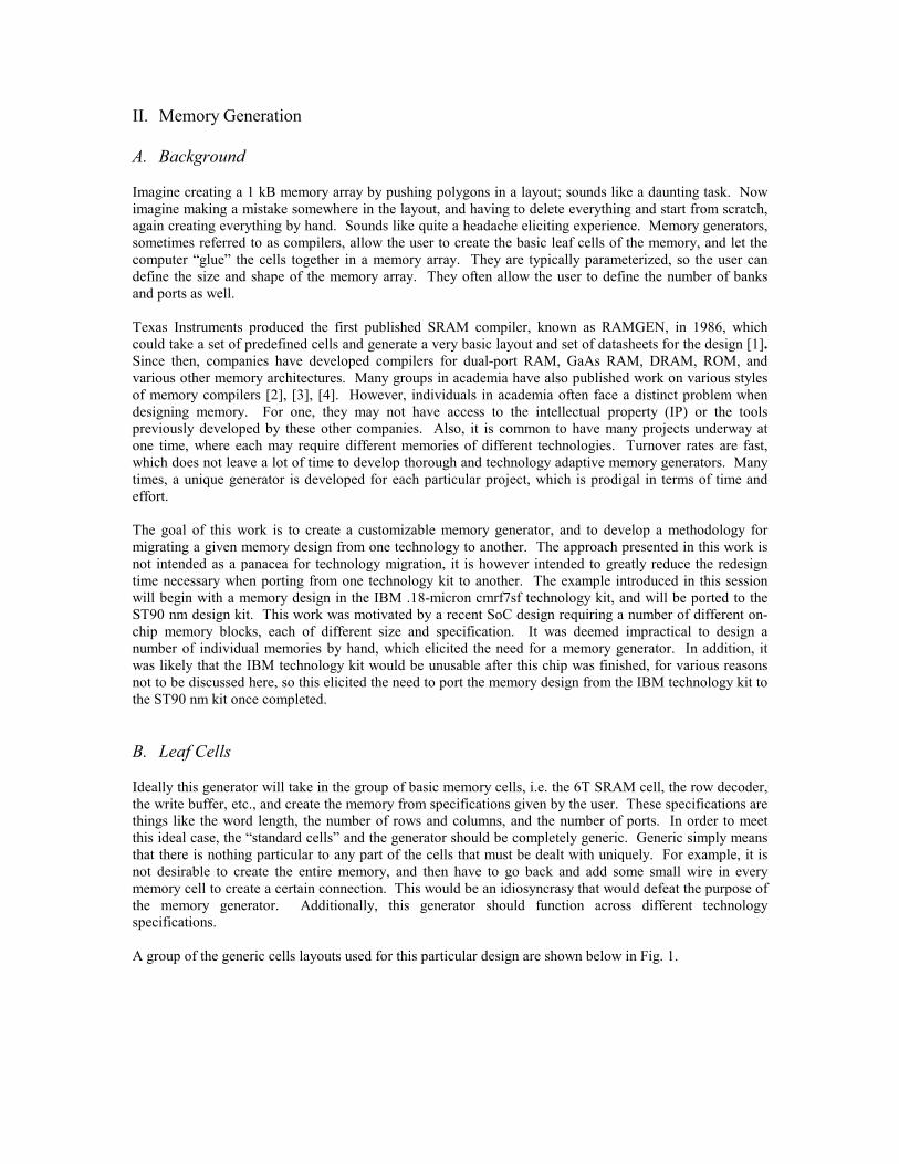
Figure 2: Block diagram of the memory design flow.
The first step is to define the specific working technology. Again, for the starting design, the specified
technology is the IBM .18 cmrf7sf design kit. In Fig. 2, under process information, it states to define the
design rule file and the interlayer capacitances and resistances. These capacitances and resistances are
important for optimization and for creating an accurate memory model in order to perform timing and
power simulations.
The next step is to define the specific characteristics of the desired memory. These characteristics include
the total size of the memory, e.g. 1, 4, or 16 kB. Additional features include how many ports the memory
needs, the type of sense amps, and possibly the types of row and column decoders. Also, it is important to
define the constraints facing the memory in this step. This means to determine what, if any, energy, delay,
area, or SNR constraints must be met for the memory to perform as expected in a given application.
Once these preliminary steps are completed, it is possible to move to the optimization block. The details of
the optimization will be lightly explored throughout the remainder of this session, however the main idea
remains that it is important to optimize the memory before laying out the final product. This optimization
can mean any number of things. The first, and most obvious step could be optimizing for performance. In
other words, using transistor sizing algorithms and detailed memory models to find the optimum memory
size and arrangement to meet a particular performance criteria. Other optimizations could include, but
aren’t limited to, power, area, and static noise margin.
The last two blocks deal with the actual memory generation. These blocks include creating the finished
layout, schematic, and model files, along with all of the timing analyses and simulated power and energy
data. The details of these two blocks are more thoroughly discussed in the next section.
D. SRAM Generation Methodology
This section states our methodology of how to create a layout generator. First, a basic flow for this task is
given.

1) Design Your Generic Memory Cells
2) Design a Small Functional Memory – Both Layout and Schematic
a. Test and Verify this Memory
b. Be Sure that the Row and Column Decoders can be Automated
3) Dump the Generic Memory Cells into SKILL Files
4) Manipulate Files to be Placed at Arbitrary X and Y Coordinates
5) Develop Memory Generator Incorporating the Generic Cells
a. Include Technology Parameter File
i. DRC File – All Inclusive
ii. User Defined File – For Quicker Implementation
b. Include Power Grid
c. Include both Layout and Model
6) Verify Memory Using the Model
The generic memory cell properties have been discussed, however there are few more important things to
note when creating these cells. First, be sure to pitch match any cells that will lie adjacent to each other in
the layout. For example, if the row decoder will attach to the left side of the memory cell array, it is
imperative to line up the power and ground lines coming from the row decoder into the memory cells. If
these wires are not pitch matched, the connection between these blocks will be awkward and will not be
conducive to automating.
The next step in building the memory generator is to design and test a small memory block. This block will
act as a template when instantiating the final memory generator. A sample memory block is shown here in
Fig. 3. This layout was created by hand, and then extracted and verified against this schematic version of
the memory block. There are a number of important ideas to note when creating this initial memory block.
First, be sure to lay out the memory in as regular a manner as possible. The more regular this initial block
is, the easier it will be to script into a generator. It is desirable to simply “glue” the individual leaf cells
together, rather than having to place small wires in between blocks to instantiate connections. Another
important thing to consider is the idea of resizing as an optimization technique. Optimization schemes
often employ transistor size adjusting in order to increase overall memory performance. It is important to
also leave some space in the design for adjustments, especially in driver cells and cells on the periphery of
the memory. Ideally, when creating memory, it is imperative to make things as small and compact as
possible, merely to save room for other circuitry in the final layout. However, most of the area of a
memory is occupied by the bit cell array itself, not the peripheral decoding and driver circuitry. This is
why it is deemed ok in this work to leave some extra room in the driver circuitry for changing transistor
sizes to meet performance and power requirements. This additional room can also help when migrating
from one technology to another, in case drastic DRC rule changes necessitate slight layout rearrangements.
E. SKILL for Layouts
Once this initial memory is designed and thoroughly tested, the next step is to start constructing the
generator. In order to do this, each leaf cell needs to be written into a script so they can be placed at
arbitrary X and Y coordinates in the layout. All Cadence layouts are defined by an underlying SKILL code
description, and this description can be obtained by “dumping” the layout into a SKILL description.
Shown below is the code to dump a Cadence layout into a SKILL script.
procedure( dumplayout(srclib cell filename)
srccellview = dbOpenCellViewByType(srclib cell "layout")
dbWriteSkill(srccellview filename "w" "5.0")
dbClose(srccellview)
)
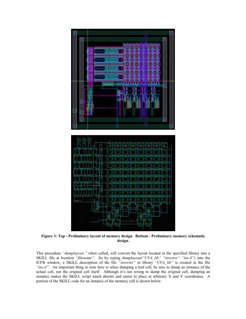
Figure 3: Top - Preliminary layout of memory design. Bottom - Preliminary memory schematic
design.
This procedure “dumplayout,” when called, will convert the layout located in the specified library into a
SKILL file at location “filename”. So by typing dumplayout(“UVA_lib” “inverter” “inv.il”) into the
ICFB window, a SKILL description of the file “inverter” in library “UVA_lib” is created in the file
“inv.il”. An important thing to note here is when dumping a leaf cell, be sure to dump an instance of the
actual cell, not the original cell itself. Although it’s not wrong to dump the original cell, dumping an
instance makes the SKILL script much shorter and easier to place at arbitrary X and Y coordinates. A
portion of the SKILL code for an instance of the memory cell is shown below.

procedure( draw_memory_cell()
dbD_312942c = dbOpenCellViewByType("UVA_MemGen_cmrf7sf"
"SRAM6T_COMP_1PORT_INST" "layout"
"maskLayout" "w")
dbD_312942c~>DBUPerUU = 1000.000000
dbD_312942c~>userUnits = "micron"
dbD_312842c = dbOpenCellViewByType("UVA_MemGen_cmrf7sf"
"SRAM6T_COMP_1PORT" "layout")
dbD_3129464 = dbCreateInst(dbD_312942c dbD_312842c "I1"
0.000000e+00:0.000000e+00 "R0" 1)
)
This code, when called, will draw an instance of the memory cell located in the file
“SRAM6T_COMP_1PORT” at the points (0,0). In order to change this code so the memory cell can be
placed at arbitrary coordinates, the code highlighted in yellow must be modified. The first highlighted code
should be replaced with “procedure( draw_memory_cell(X Y)”, and in the second highlighted section, the
0’s should be changed to the variables x and y. The final product would read something like this.
procedure( draw_memory_cell(X Y)
dbD_312942c = dbOpenCellViewByType("UVA_MemGen_cmrf7sf"
"SRAM6T_COMP_1PORT_INST" "layout"
"maskLayout" "w")
dbD_312942c~>DBUPerUU = 1000.000000
dbD_312942c~>userUnits = "micron"
dbD_312842c = dbOpenCellViewByType("UVA_MemGen_cmrf7sf"
"SRAM6T_COMP_1PORT" "layout")
dbD_3129464 = dbCreateInst(dbD_312942c dbD_312842c "I1"
X:Y "R0" 1)
)
It is possible to modify this code either by hand or by using Perl scripting, however since the number of
leaf cells is fairly small, these modifications were performed by hand.
F. Row Decoder Design
The next step is to create a script, which will use the newly created SKILL files of these leaf cells to create
the entire memory layout. The idea here is to write a script, or set of scripts, that will create the small
memory that was designed and tested in a previous step. The basic memory cell array, coupled with the
precharge cells and decoder drivers, will not be discussed in great detail here, mainly because scripting the
placement of these cells is fairly straightforward. It is possible to use simple nested for loops to position
the memory cells at the necessary X and Y coordinates to create the array. A small example of this is
shown later in this section, however the majority of this section will focus on designing and scripting the
row and column decoders. Lastly this section will discuss the power grid.
Since a large portion of this session is devoted to technology adaptation, it is important to design the row
and column decoders with portability in mind. What this means is to again, leave enough space in the
design to adapt to different technology specifications, and to also design with as much regularity as
possible. The main reason for leaving space is for porting to a different technology of the same or larger
size. Regularity becomes very important when scaling down in size. If there are lots of parallel wires in a
given block, it is easy to take advantage of the size scaling because decreasing the wire width does not
affect any other wires in the block. However, when there are lots of odd, non-parallel wire runs, decreasing
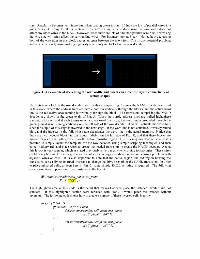
the wire size will often affect the surrounding wires. For instance, look at Fig. 4. Notice how decreasing
both of the wire sizes in this block causes an open between the two wires. This is one potential problem,
and others can easily arise, making regularity a necessity in blocks like the row decoder.
Figure 4: An example of decreasing the wire width, and how it can affect the layout connectivity of
certain shapes.
Next lets take a look at the row decoder used for this example. Fig. 5 shows the NAND row decoder used
in this work, where the address lines are purple and run vertically through the blocks, and the actual word
line is the red active area running horizontally through the block. The transistors comprising the NAND
decoder are shown in the green ovals of Fig. 5. When the purple address lines are pulled high, these
transistors turn on, and if each transistor on a given word line is on, the word line is grounded through the
green ground wire running vertically on the left side of the row decoder. This will activate the word line,
since the output of this stage is inverted in the next stage. If the word line is not activated, it weakly pulled
high, and the inverter in the following stage deactivates the word line in the actual memory. Notice that
there are two decoder blocks in this figure (labeled on the left side of Fig. 5), and that these blocks are
mirror images of each other, except for the active transistor region. This is a very nice feature because it is
possible to simply layout the template for the row decoder, using simple scripting techniques, and then
come in afterwards and place wires to create the needed transistors to create the NAND decoder. Again,
this layout is very regular, which as stated previously is very nice when crossing technologies. These wires
could easily be shrank or enlarged to meet another technology specification, without causing problems with
adjacent wires or cells. It is also important to note that the active region, the red region housing the
transistors, can easily be enlarged or shrank to change the drive strength of the NAND transistors. In order
to place mirrored cells, as seen here in Fig. 5, some simple SKILL scripting is required. The following
code shows how to place a mirrored instance in the layout.
dbCreateInst(window cell_name inst_name
X : Y “MX” 1)
The highlighted area in this code is the detail that makes Cadence place the instance inverted and not
standard. If this highlighted section were replaced with “R0”, it would place the instance without
inversion. The following code shows how to create a number of these inverted cells in a row.
for( j 0 (2**n)– 1)
if( modulo( j 2 ) == 1 then
dbCreateInst(window cell_name inst_name
X : Y_pitch*j “R0” 1)
else
dbCreateInst(window cell_name inst_name
X : Y_pitch*j “MX” 1)
)
)

When this script is ran, 2n cells will be created stacked vertically on top of each other, where every other
cell is inverted from the previous one. These same scripting techniques can be used to generate the basic
memory cell array as well, since most memory cells are capable of being mirrored to save space.
Figure 5: A portion of the NAND row decoder. Sections A and B are mirror images of each other
over the horizontal axis, except for the transistor placement (green ovals).
G. Column Decoder and Power Ring Design
Next lets examine the column decoder. Again, notice the regularity in Fig. 6, where the address lines all
run horizontally through the binary tree column decoder. A few sets of address lines are circled in green,
and these wires run through the entire decoder tree, whereas the red circles denote simple interconnects
between various levels of the tree. Even from looking at the layout, it is easy to see the different levels of
NFET pass transistors, of which a few are circled in white. The scripting to generate this column decoder
can be created using the same basic techniques as discussed with the row decoder, using basic nested for
loops to place instances of NFETs, and join them with interconnect. One main point to note here is to
design the decoders with as much regularity as possible. This design regularity will save the user many
hours of tedious scripting.
Figure 6: Portion of the tree column decoder. A few address lines are circled in green, some
interconnect wires are circled in red, and a few decoder NFETs are circled in white.

The last thing to discuss in this section is the power grid. This grid can be seen in Fig. 3 presented earlier
in this paper. The grid consists of the power ring surrounding the entire memory area, and the vertical
power and ground lines that run vertically through the memory array. Again, notice how the regularity of
the memory cell array elicits easy connections from the power grid to the interior of the SRAM, since all of
the Vdd and ground lines run horizontally through the entire memory block. Another important idea to
note about creating the power grid is to simply make sure the wires are very wide, as to provide as little
resistance to current flow as possible. For this design, the wires are approximately 3 microns wide,
however ideally this power grid width should be parameterized in the memory generator so the user can
size the grid appropriately. Also, it is beneficial to add lots of power grid connections into the memory cell
array. Fig. 3 only shows one vertical power and ground connection to the interior of the cell array, but this
is because the memory array is fairly small. As the array grows larger, it is beneficial to at least have
connections once every 25 to 50 microns. Multiple grid connections can be seen later in this work in Fig.
20.

III. Crossing Technologies
A. Importance of Technology Migration
The main goal of this work is to develop a memory generator that can easily span across technologies. This
compiler is called technology “adaptive” for a specific reason. Ideally the generator could be totally
technology independent, where the user could build a generic memory block, and have a set of scripts
convert the entire layout into different design kits. Although this sounds appealing, it does not make a lot
of sense in reality, for two main reasons. First, a nice feature of technology scaling is that the engineer can
really take advantage of decreasing feature sizes in order to compact overall cell sizes. This is often easier
to do manually then it is to do through automation. Take for instance the 6T memory cell. More often then
not, when a new, smaller feature size design kit arrives, engineers will totally rework the memory cell to
make it smaller and to increase the density of the memory array. Technology “adaptive” simply means the
user can redesign certain cells, while using the compiler to migrate certain portions of the layout, such as
the row and column decoders, to a new design kit. The second trouble in creating a perfectly technology
independent generator is that there are often very large and unexpected DRC rule changes from one design
kit to another. While some DRC rule changes can be handled simply through scripting, other drastic DRC
rule changes could mandate manual redesign of certain portions of a layout. On top of this, some
technology kits have layers that others may not have. For instance some kits have a P-well layer,
contributing to a triple well technology, while others do not have this feature. These things must be
manually taken care of after the technology crossing. Technology migration is meant as a tool to cut down
on redesign time when converting between two design kits, not as a total panacea to convert between
technologies.
Although not perfect, this product is a very valuable tool in academia, and could also prove valuable in
industry. Performing academic research in circuits often involves exploring designs in numerous
technologies in order to fully characterize and evaluate certain performance characteristics. It is therefore
necessary to have some tool capable of aiding in transporting designs from one technology to another in a
timely manner. In industry, companies do not change toolkits as often as in academia, however it is not
uncommon for a company to utilize more than one technology kit, especially for work amongst different
projects. The main goal of this work is to develop a tool that elicits a fast time-to-market response when
converting memory from one technology to another. These techniques could be very useful for a small
company, with limited resources, looking for a fast time-to-market response when developing new products
in new design kits.
B. Back-End Technology Migration
There are two ways to think about bridging designs across technologies. The first is a back end process,
where the design is completely finished, and scripting techniques are used to simply modify layer
assignments in the design to port the layout into a different technology. The second is to incorporate the
adaptation into the compiler itself. Both methods require similar amounts of work to implement, and each
method is utilized for unique tasks within the technology migration process. Both techniques are discussed
in this section, starting with the back end, modification style process.
First let’s list a generic flow for the back end modification process.
1) Dump the finished layout into a SKILL file
2) Perform a layer conversion using a scripting method
3) Import the SKILL code into the new technology kit with the modified layer information
A 6T SRAM cell is used to demonstrate this flow by converting it from the .18 um IBM7SF kit to the 90
nm ST90 design kit. The scripting used to dump a layout into a SKILL description was demonstrated in
Section II-C, so it will not be revisited here, however a partial SKILL description of a layout is shown
below in Fig. 7. When these layouts are dumped into SKILL descriptions, it is apparent that a few

instructions are repeatedly used to draw blocks and figures in the layouts. Two of these commands are
dbCreateRect and dbCreatePath, one of which is shown in Fig. 7. Fig. 7 shows a command that looks
similar to this:
dbD_3a2d434 = dbCreateRect(dbD_39f582c list(12 252)
list( x1:y1 x2:y2))
This instruction will draw a rectangle from the corners of (x1, y1) to (x2, y2) using the layer specified in
the highlighted region. This layer happens to the first metal layer, which can be found in the
documentation accompanying the design kit. Each layer, i.e. metal, active, n-well, etc, is associated with a
particular number, which is referred to as the “layer index” in this work.
Figure 7: Portion of SKILL code from an inverter layout.
If this SKILL script were directly imported into a different technology kit, Cadence would display blocks in
the layout according to the positions specified in the scripting, however the layer indices would not likely
coincide with the proper layers of the new technology kit. The result would be a non-functioning layout,
that somewhat resembled the original design. In order to correctly import this SKILL file across
technologies, it is imperative to update these layer indices to match the new design kit without changing
any other code in the SKILL scripts. This feat is easily accomplished through Perl scripting methods.
Perl is a very common scripting language, and is regularly used for searching and replacing text lines
within files. Below is an excerpt from a script to replace layer indices in a SKILL file. For example, in
Fig. 8, the command s/$M1/$M1ST/g will locate the string variable $M1 in the current line of text and replace it with the variable $M1ST. The small g simply makes this function act globally, so this function
will act on all lines of text. Fig 8 shows the result of transforming the 6T memory cell shown in the
IBM7SF kit into the ST90 nm library using the script shown on the left side of Fig. 8.
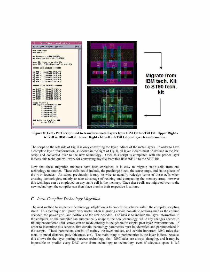
Figure 8: Left - Perl Script used to transform metal layers from IBM kit to ST90 kit. Upper Right -
6T cell in IBM toolkit. Lower Right - 6T cell in ST90 kit post layer transformation.
The script on the left side of Fig. 8 is only converting the layer indices of the metal layers. In order to have
a complete layer transformation, as shown in the right of Fig. 8, all layer indices must be defined in the Perl
script and converted over to the new technology. Once this script is completed with the proper layer
indices, this technique will work for converting any file from this IBM7SF kit to the ST90 kit.
Now that these migration methods have been explained, it is easy to migrate static cells from one
technology to another. These cells could include, the precharge block, the sense amps, and static pieces of
the row decoder. As stated previously, it may be wise to actually redesign some of these cells when
crossing technologies, mainly to take advantage of resizing and compacting the memory array, however
this technique can be employed on any static cell in the memory. Once these cells are migrated over to the
new technology, the compiler can then place them in their respective locations.
C. Intra-Compiler Technology Migration
The next method to implement technology adaptation is to embed this scheme within the compiler scripting
itself. This technique will prove very useful when migrating certain non-static sections such as the column
decoder, the power grid, and portions of the row decoder. The idea is to include the layer information in
the compiler, so the compiler can automatically adapt to the new technology, while any changes needed to
fix any encountered DRC errors can be made directly to the generator scripts, post layer transformation. In
order to instantiate this scheme, first certain technology parameters must be identified and parameterized in
the scripts. These parameters consist of mainly the layer indices, and certain important DRC rules (i.e.
metal to metal distance, poly thickness, etc). The main thing to parameterize is the layer indices, because
this allows for the layer porting between technology kits. DRC rules are always changing, and it may be
impossible to predict every DRC error from technology to technology, even if adequate space is left
between all blocks in the layout. These DRC errors can easily be corrected in the event that they do arise
by manually tweaking the scripts.
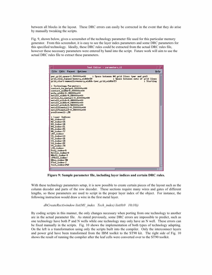
Fig. 9, shown below, gives a screenshot of the technology parameter file used for this particular memory
generator. From this screenshot, it is easy to see the layer index parameters and some DRC parameters for
this specified technology. Ideally, these DRC rules could be extracted from the actual DRC rules file,
however these necessary parameters were entered by hand into the script. Future work will aim to use the
actual DRC rules file to extract these parameters.
Figure 9: Sample parameter file, including layer indices and certain DRC rules.
With these technology parameters setup, it is now possible to create certain pieces of the layout such as the
column decoder and parts of the row decoder. These sections require many wires and gates of different
lengths, so these parameters are used to script in the proper layer index of the object. For instance, the
following instruction would draw a wire in the first metal layer.
dbCreateRect(window list(M1_index Tech_index) list(0:0 10:10))
By coding scripts in this manner, the only changes necessary when porting from one technology to another
are in the actual parameter file. As stated previously, some DRC errors are impossible to predict, such as
one technology have both P and N wells while one technology may only have an N well. These errors can
be fixed manually in the scripts. Fig. 10 shows the implementation of both types of technology adapting.
On the left is a transformation using only the scripts built into the compiler. Only the interconnect layers
and power grid have been transformed from the IBM toolkit to the ST90 kit. The right side of Fig. 10
shows the result of running the compiler after the leaf cells were converted over to the ST90 toolkit.
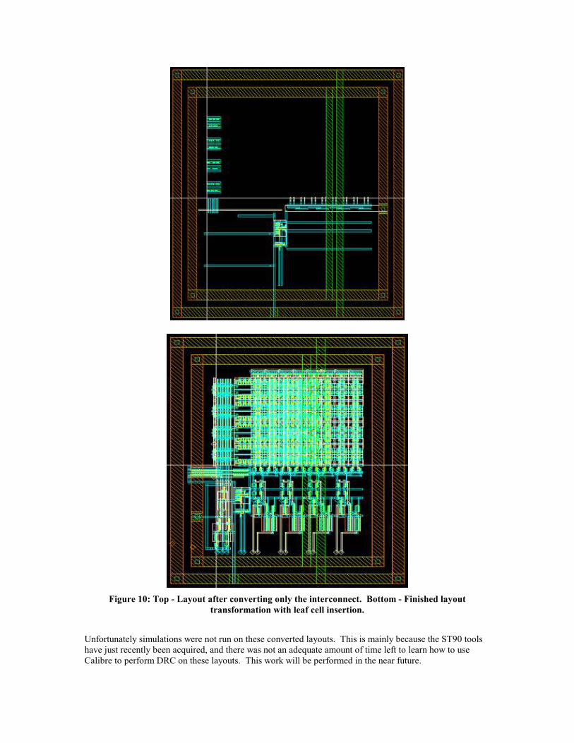
Figure 10: Top - Layout after converting only the interconnect. Bottom - Finished layout
transformation with leaf cell insertion.
Unfortunately simulations were not run on these converted layouts. This is mainly because the ST90 tools
have just recently been acquired, and there was not an adequate amount of time left to learn how to use
Calibre to perform DRC on these layouts. This work will be performed in the near future.

IV. Simulating and Optimizing
A. Automating Simulations
When developing a memory, it is imperative to simulate the final product in order to verify the timing
features and the power consumption. It would be terrible to have to manually simulate the memory after
every generation. In order to prevent this, this section introduces a method to automatically simulate
blocks using Ocean scripting combined with Cadence SKILL. These same methods are also utilized in the
optimization process. The focus of this work is not optimization, but this section will introduce some
methods to optimize in an automated fashion.
In order to automate the simulations, the first step is to implement the desired simulations in the Analog
Environment. This means to set up all of the stimuli, variables, model files, and anything else necessary to
perform the required simulations. The underlying scripting used to instantiate simulations in the Analog
Environment is Ocean. Once these simulations are setup, they can be transferred into Ocean scripts for
manual modification or to be called from outside of the Analog Environment. Fig.11 shows the Analog
Environment window and highlights the proper objects to select to convert simulations into Ocean scripts.
Figure 11: The Cadence Analog Environment window. In the upper left, the Save Script command is
highlighted, denoting how to transfer simulations into Ocean scripts.
The “Save Script” command highlighted will convert these simulations into Ocean scripts. Fig. 12 shows
an example of a created Ocean script. It is fairly straightforward to understand this script. Basically, it
defines certain necessary files such as the model files and stimuli files, then it defines certain circuit
variables, and then it runs and plots the simulated results. In order to automate the simulations for the
memory, several things need to be updated in this script. The first thing to change is to parameterize the
variables in the scripts. This is in case the user wants to change some of the internal simulation variables
when simulating the memory. Also it is imperative to parameterize the file inputs into the scripts, such as
the stimuli, model, and design files. This is so the user can change the files to simulate and model files if
need be. Fig. 13 highlights these changes to the original Ocean script.
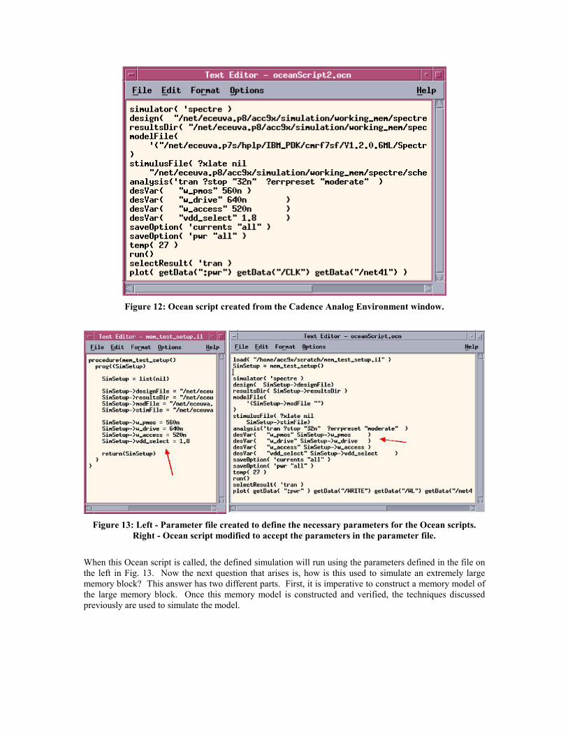
Figure 12: Ocean script created from the Cadence Analog Environment window.
Figure 13: Left - Parameter file created to define the necessary parameters for the Ocean scripts.
Right - Ocean script modified to accept the parameters in the parameter file.
When this Ocean script is called, the defined simulation will run using the parameters defined in the file on
the left in Fig. 13. Now the next question that arises is, how is this used to simulate an extremely large
memory block? This answer has two different parts. First, it is imperative to construct a memory model of
the large memory block. Once this memory model is constructed and verified, the techniques discussed
previously are used to simulate the model.

B. Memory Modeling and Final Simulations
Memory models can be very extensive and tedious to accurately create. This work will not discuss the
details of creating the memory model, it will simply introduce the model used for this work and why it is
conducive to both automated simulations and technology adaptation. Fig. 14 shows the basic structure for
the memory model used in this work.
Figure 14: Basic structure of the memory model used for this memory generator.
There are basically three blocks in this memory model. The first are the normal bit cells used in the
generated memory, represented by the blue squares. The next are the dummy bit cells, represented by the
red pentagons. This cell is sized to account for the load and leakage generated by all of the memory cells
except for the four normal bit cells on the corners. Lastly, the green circles represent the RC delays of the
interconnect in the memory. For purposes of this discussion, the most important feature of this model is
that it is fully parameterized. The reason for this is that only one model is needed for each technology kit,
as long as the model is fully parameterized. Each time a new memory is generated, the schematic
parameters in this model can simply be updated to represent the new layout. For instance, the bit cell
should have all of the 6T cell transistor widths and Vdd potentials as variables. The dummy bit cells
should also have the transistor widths and Vdd potentials as variables, except the widths of the transistors
should vary with the size of the memory. For example, if there are 256 cells on a row, each dummy bit cell
should represent the load and leakage of 127 cells (since there are two dummy bit cells per row and
column), which would equate to sizing the transistors widths 127 times larger than their original values.
Additionally, the RC delays should vary in a similar matter, as they will increase proportionally with the
memory size. This model, as constructed in Cadence is shown in Fig. 15.

Figure 15: Cadence schematic of the memory model introduced in Fig. 14.
The next step is to use this model to construct automated simulations of the entire memory. The techniques
discussed in the previous section are used in order to instantiate this step. First, it would be imperative to
create the necessary simulations (timing analysis, power, etc) in the analog environment, and write these
simulations out to Ocean files as discussed previously. Then the parameter file should be created, as shown
in Fig. 13. Now every time a new memory is generated, the compiler should feed the transistor size,
memory size, and Vdd potential information to this parameter file. Once this is completed, the
parameterized Ocean script is ready for operation. Running these scripts will yield results that look
something like what is shown in Fig. 16.
Figure 16: Simulated memory model. Simulation shows two read and write cycles, all of which are
writing to the upper right corner of the memory.
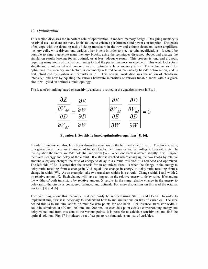
C. Optimization
This section discusses the important role of optimization in modern memory design. Designing memory is
no trivial task, as there are many knobs to tune to enhance performance and power consumption. Designers
often cope with the daunting task of sizing transistors in the row and column decoders, sense amplifiers,
memory cells, write drivers, and various other blocks in order to meet certain specifications. It would be
possible to simply generate many memory blocks, using the techniques discussed above, and analyze the
simulation results looking for an optimal, or at least adequate result. This process is long and arduous,
requiring many hours of manual cell tuning to find the perfect memory arrangement. This work looks for a
slightly more automated and concrete way to optimize a large memory array. The technique used for
optimizing this memory architecture is commonly referred to as “sensitivity based” optimization, and is
first introduced by Zyuban and Strenski in [5]. This original work discusses the notion of “hardware
intensity,” and how by equating the various hardware intensities of various tunable knobs within a given
circuit will yield an optimal circuit topology.
The idea of optimizing based on sensitivity analysis is rooted in the equation shown in Eq. 1.
Equation 1: Sensitivity based optimization equations [5], [6].
In order to understand this, let’s break down the equation on the left hand side of Eq. 1. The basic idea is,
in a given circuit there are a number of tunable knobs, i.e. transistor widths, voltages, thresholds, etc. In
this equation the knobs are Vdd potential and width (W). When one knob is altered slightly, it will impact
the overall energy and delay of the circuit. If a state is reached where changing the two knobs by relative
amount X equally changes the ratio of energy to delay in a circuit, this circuit is balanced and optimized.
The left side of Eq. 1 states that the criteria for an optimized circuit is when the change in the energy to
delay ratio resulting from a change in Vdd equals the change in energy to delay ratio resulting from a
change in width (W). As an example, take two transistor widths in a circuit. Change width 1 and width 2
by relative amount X. Each change will have an impact on the relative energy to delay ratio. If changing
the widths of both transistors by relative amount X results in the same relative change in the energy to
delay ratio, the circuit is considered balanced and optimal. For more discussions on this read the original
works in [5] and [6].
The nice thing about this technique is it can easily be scripted using SKILL and Ocean. In order to
implement this, first it is necessary to understand how to run simulations on lists of variables. The idea
behind this is to run simulations on multiple data points for one knob. For instance, transistor width 1
could be simulated at 500 nm, 700 nm, and 900 nm. At each data point exists a corresponding energy and
delay value, and from this data at the various points, it is possible to calculate sensitivities and find the
optimal solution. Fig. 17 introduces a set of scripts to run simulations on lists of variables.
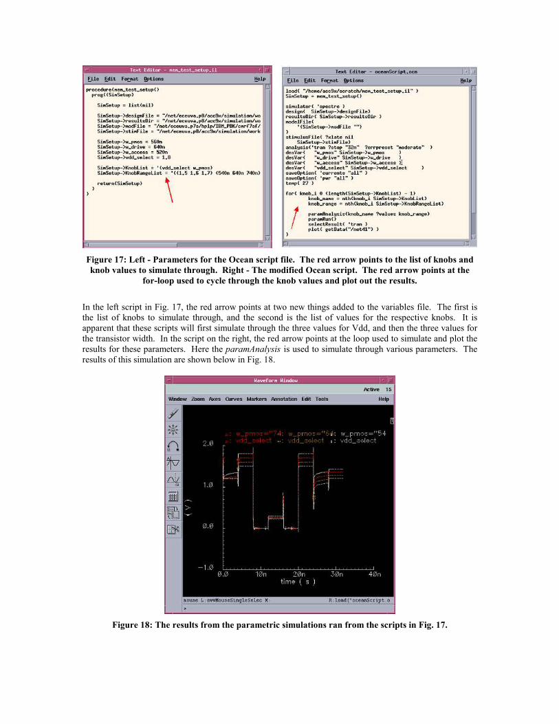
Figure 17: Left - Parameters for the Ocean script file. The red arrow points to the list of knobs and
knob values to simulate through. Right - The modified Ocean script. The red arrow points at the
for-loop used to cycle through the knob values and plot out the results.
In the left script in Fig. 17, the red arrow points at two new things added to the variables file. The first is
the list of knobs to simulate through, and the second is the list of values for the respective knobs. It is
apparent that these scripts will first simulate through the three values for Vdd, and then the three values for
the transistor width. In the script on the right, the red arrow points at the loop used to simulate and plot the
results for these parameters. Here the paramAnalysis is used to simulate through various parameters. The results of this simulation are shown below in Fig. 18.
Figure 18: The results from the parametric simulations ran from the scripts in Fig. 17.

Now that schematics can be simulated with multiple variables and multiple parameters per variable, it is
possible to optimize the circuit using the previously discussed techniques. As an example, let’s discuss
how to equate the sensitivities of two transistor widths in a circuit. First, as shown previously, set the
scripts up with the proper lists of variables and variable values. For this example, let’s say that both
transistors will be simulated at 500 and 600 nm. Using the scripts, run through the simulations for the first
transistor. For each width, observe the average circuit energy and the critical delay. Using the equations
shown in Eq. 1, it is possible to calculate the sensitivity for this first width. Divide the change in energy by
the change in width, and then divide this total by the ratio of the change in delay to the change in width.
Now repeat this step for the second transistor width, and if these calculated sensitivities are equal, then the
circuit is balanced and optimized. All of this math can be scripted using basic Ocean scripting techniques,
which are not shown here. It is not likely that the sensitivities will be equal on the first run, so this often
yields a number of various energy and delay curves for different transistor widths. Fig. 19 shows the
results of optimizing a bit cell based on this technique. One thing to notice is that there are multiple
optimal solutions, according to what voltage the cell operates at. This technique can be extended to
optimizing the entire memory, i.e. number of banks, driver strengths, types of sense amps, etc. Right now,
this work is still in progress, but as stated previously, Fig. 19 does show some preliminary results from the
optimization sequence.
Figure 19: Optimization results from optimizing one bit cell in the memory array.
V. RTL Compiler, Abstract Generator and Encounter Flow
A. RTL Compiler
Now that it has been shown how to generate, simulate and optimize memories, this session will conclude
with a discussion of the incorporating the final layout into an automated design flow. With the onset of
designs such as SoCs and NoCs, typically incorporating millions of transistors onto one die, it is often
useful to utilize a top-down design methodology. This way, users can develop verilog / VHDL descriptions
of their projects, implement and verify them on an FPGA, and use software, such as Cadence’s RTL
Compiler, to transfer these high level descriptions down to a silicon layout. RTL Compiler is specifically
used to translate a HDL description down into a netlist that can be processed further down into a layout.
This section will specifically discuss how to incorporate custom circuits, such as the large memory blocks
discussed in the previous sections, into this top-down design flow.
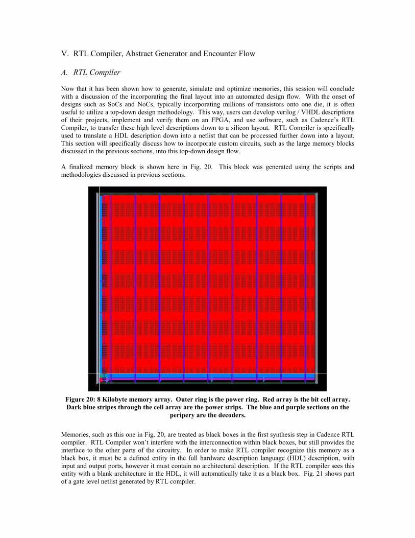
A finalized memory block is shown here in Fig. 20. This block was generated using the scripts and
methodologies discussed in previous sections.
Figure 20: 8 Kilobyte memory array. Outer ring is the power ring. Red array is the bit cell array.
Dark blue stripes through the cell array are the power strips. The blue and purple sections on the
peripery are the decoders.
Memories, such as this one in Fig. 20, are treated as black boxes in the first synthesis step in Cadence RTL
compiler. RTL Compiler won’t interfere with the interconnection within black boxes, but still provides the
interface to the other parts of the circuitry. In order to make RTL compiler recognize this memory as a
black box, it must be a defined entity in the full hardware description language (HDL) description, with
input and output ports, however it must contain no architectural description. If the RTL compiler sees this
entity with a blank architecture in the HDL, it will automatically take it as a black box. Fig. 21 shows part
of a gate level netlist generated by RTL compiler.
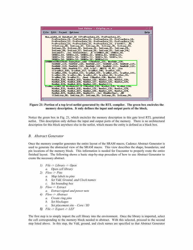
Figure 21: Portion of a top level netlist generated by the RTL compiler. The green box encircles the
memory description. It only defines the input and output ports of the block.
Notice the green box in Fig. 21, which encircles the memory description in this gate level RTL generated
netlist. This description only defines the input and output ports of the memory. There is no architectural
description for this block anywhere else in the netlist, which means the entity is defined as a black box.
B. Abstract Generator
Once the memory compiler generates the entire layout of the SRAM macro, Cadence Abstract Generator is
used to generate the abstracted view of the SRAM macro. This view describes the shape, boundaries, and
pin locations of the memory block. This information is needed for Encounter to properly route the entire
finished layout. The following shows a basic step-by-step procedure of how to use Abstract Generator to
create the necessary abstract.
1) File -> Library -> Open
a. Open cell library
2) Flow -> Pins
a. Map labels to pins
b. Set Vdd, Ground, and Clock names
c. Set bounding box
3) Flow -> Extract
a. Extract signal and power nets
4) Flow -> Abstract
a. Create ring pins
b. Set blockages
c. Set placement site – Core / IO
5) File -> Export -> LEF
The first step is to simply import the cell library into the environment. Once the library is imported, select
the cell corresponding to the memory block needed to abstract. With this selected, proceed to the second
step listed above. In this step, the Vdd, ground, and clock names are specified so that Abstract Generator
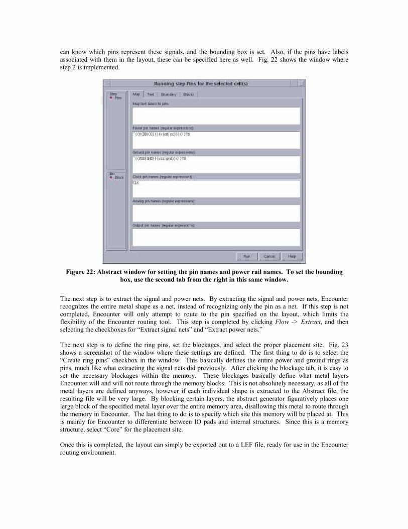
can know which pins represent these signals, and the bounding box is set. Also, if the pins have labels
associated with them in the layout, these can be specified here as well. Fig. 22 shows the window where
step 2 is implemented.
Figure 22: Abstract window for setting the pin names and power rail names. To set the bounding
box, use the second tab from the right in this same window.
The next step is to extract the signal and power nets. By extracting the signal and power nets, Encounter
recognizes the entire metal shape as a net, instead of recognizing only the pin as a net. If this step is not
completed, Encounter will only attempt to route to the pin specified on the layout, which limits the
flexibility of the Encounter routing tool. This step is completed by clicking Flow -> Extract, and then
selecting the checkboxes for “Extract signal nets” and “Extract power nets.”
The next step is to define the ring pins, set the blockages, and select the proper placement site. Fig. 23
shows a screenshot of the window where these settings are defined. The first thing to do is to select the
“Create ring pins” checkbox in the window. This basically defines the entire power and ground rings as
pins, much like what extracting the signal nets did previously. After clicking the blockage tab, it is easy to
set the necessary blockages within the memory. These blockages basically define what metal layers
Encounter will and will not route through the memory blocks. This is not absolutely necessary, as all of the
metal layers are defined anyways, however if each individual shape is extracted to the Abstract file, the
resulting file will be very large. By blocking certain layers, the abstract generator figuratively places one
large block of the specified metal layer over the entire memory area, disallowing this metal to route through
the memory in Encounter. The last thing to do is to specify which site this memory will be placed at. This
is mainly for Encounter to differentiate between IO pads and internal structures. Since this is a memory
structure, select “Core” for the placement site.
Once this is completed, the layout can simply be exported out to a LEF file, ready for use in the Encounter
routing environment.

Figure 23: Screenshot of the window to create the ring pins, set the blockages,
and select the proper placement site.
C. Encounter
The last step needed to incorporate these custom memory blocks into the top-down design flow is to use
Encounter to route the blocks. This step is fairly straightforward, so long as the previous steps were
completed correctly. Once the entire RTL netlist is created, and all of the abstracts are generated, loading
the entire netlist into Encounter will look something like what is shown in Fig. 24. The medium sized
squares on the lower right hand side of the figure are the custom memory blocks. In this example there are
eight total blocks although only seven are actually shown in this figure.
Once the netlist is imported, these blocks can simply be placed anywhere in the die area. As long as the
nets and power grids were extracted properly in the abstract generator, Encounter should have no problem
routing to the proper nets once the routing starts. A final layout in Encounter is shown in Fig. 25, and a
section of the final layout in shown in Fig. 26. Notice in Fig. 26 how the power grid lines are routed
directly to memory power ring at the point in which they happen to land. This is possible since the whole
power ring in the memory is considered a pin, making it easy for Encounter to route the power wires.
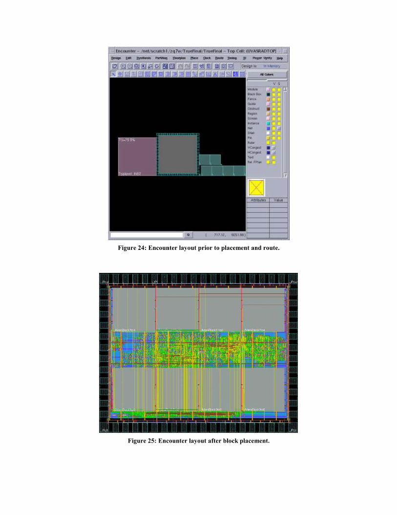
Figure 24: Encounter layout prior to placement and route.
Figure 25: Encounter layout after block placement.

Figure 26: Encounter photo taken after placement and routing. Notice how the power grid wires
route directly to the power rings of the memory blocks.
VI. Conclusion
This work has introduced the design methodology for a technology adaptive memory generator. The entire
design flow was presented, including scripting methods for creating the compiler, techniques for migrating
layouts between two design kits, and some preliminary approaches for overall memory optimization.
Examples were given to show how to transport layouts from on technology to another, and to show the
flexibility of the memory generator. Simulations verify that the memory works as expected.
Future work may consist of exploring more technologies in which to port this memory. Additionally,
optimization techniques will be further developed, aiming to create an optimal memory design for any set
design specifications. The finished product hopes to optimize the design up front, i.e. determine the correct
number of banks, optimal transistor sizing, etc, and layout and simulate the memory according to these
derived specifications.
VII. References
[1] W. Swartz, C. Giuffre, W. Banzhaf, M. deWit, H. Khan, C. McIntosh, T. Pavey, and D. Thomas,
"CMOS RAM, ROM, and PLA Generators for ASIC Applications," Proceedings of the 1986 IEEE Custom
Integrated Circuits Conference, pp. 334 - 338.
[2] H. Shinohara, N. Matsumoto, K. Fujimori, Y. Tsujihashi, H. Nakao, S. Kato, Y. Horiba, A. Tada, “A
Flexible Multiport RAM Compiler for Datapath,” IEEE Journal of Solid-State Circuits, Vol. 26, No. 3,
March 1991.
[3] K. Chakraborty, S. Kulkarni, M. Bhattacharya, P. Mazumder, A. Gupta, “A Physical Design Tool for
Built-In Self-Repairable RAMs,” IEEE Transactions on VLSI, Vol. 9, No. 2, April 2001.
[4] A. Chandna, C. D. Kibler, R. B. Brown, M. Roberts, K. A. Sakallah, “The Aurora RAM Compiler,”
Proceedings of the 32nd ACM/IEEE Design Automation Conference, pp. 261-266, 1995.
[5] V. Zyuban, P. Strenski, “Unified Methodology for Resolving Power-Performance Tradeoffs at the
Microarchitectural and Circuit Levels,” Proceedings of the 2002 International Symposium on Low Power
Electronics and Design, pp. 166 – 171, 2002.
[6] D. Markovic, V. Stojanovic, B. Nikolic, M. A. Horowitz, R. W. Brodersen, “Methods for True Energy-
Performance Optimization,” IEEE Journal of Solid-State Circuits, Vol. 39, No. 8, August 2004.
Recommended