A BASIC, FOUR LOGIC CLUSTER, DISJOINT
SWITCH CONNECTED FPGA ARCHITECTURE
A SENIOR PROJECT REPORT
Submitted in partial fulfillment of the requirements for the award of the degree of
BACHELOR OF SCIENCE
IN
COMPUTER ENGINEERING
by
JOSEPH PRACHAR
Under the guidance of
Dr. Tina Smilkstein
Department of Computer Engineering
California Polytechnic State University, San Luis Obispo
June 2018

Abstract
This paper seeks to describe the process of developing a new FPGA architecture
from nothing, both in terms of knowledge about FPGAs and in initial design material.
Specifically, this project set out to design an FPGA architecture which can implement
a simple state machine type design with 10 inputs, 10 outputs and 10 states. The
open source Verilog-to-Routing FPGA CAD flow tool was used in order to synthesize,
place, and route HDL files onto the architecture. This project was completed in terms
of the spirit of the original goals of implementing an FPGA from scratch. Although,
the project resulted in an architecture which slightly underperformed in its ability to
route 100% of 10 input, 10 output, 10 state designs due to the general place and route
algorithm used and the lack of non-contrived 10 input 10 output 10 state FSM designs.
1

Contents
1 Introduction 5
1.1 Overview . . . . . . . . . . . . . . . . . . . . . . . . . . . . . . . . . . . . . . 5
1.2 Basic Logic Element . . . . . . . . . . . . . . . . . . . . . . . . . . . . . . . 6
1.3 Connection Box . . . . . . . . . . . . . . . . . . . . . . . . . . . . . . . . . . 7
1.4 Logic Cluster . . . . . . . . . . . . . . . . . . . . . . . . . . . . . . . . . . . 8
1.5 Switch Block . . . . . . . . . . . . . . . . . . . . . . . . . . . . . . . . . . . 9
1.6 Input/Output Block . . . . . . . . . . . . . . . . . . . . . . . . . . . . . . . 10
1.7 Architecture . . . . . . . . . . . . . . . . . . . . . . . . . . . . . . . . . . . . 11
1.8 Design Approach . . . . . . . . . . . . . . . . . . . . . . . . . . . . . . . . . 12
1.9 Report Organization . . . . . . . . . . . . . . . . . . . . . . . . . . . . . . . 13
2 Circuit Design 14
2.1 Architecture . . . . . . . . . . . . . . . . . . . . . . . . . . . . . . . . . . . . 14
2.2 Programming Circuit . . . . . . . . . . . . . . . . . . . . . . . . . . . . . . . 16
2.3 Basic Logic Element . . . . . . . . . . . . . . . . . . . . . . . . . . . . . . . 17
2.4 Connection Box . . . . . . . . . . . . . . . . . . . . . . . . . . . . . . . . . . 18
2.5 Logic Cluster . . . . . . . . . . . . . . . . . . . . . . . . . . . . . . . . . . . 19
2.6 Switch Block . . . . . . . . . . . . . . . . . . . . . . . . . . . . . . . . . . . 20
2.7 Input/Output Block . . . . . . . . . . . . . . . . . . . . . . . . . . . . . . . 20
3 Verilog-to-Routing 21
3.1 Introduction . . . . . . . . . . . . . . . . . . . . . . . . . . . . . . . . . . . . 21
3.2 Architecture Description . . . . . . . . . . . . . . . . . . . . . . . . . . . . . 22
3.3 Example . . . . . . . . . . . . . . . . . . . . . . . . . . . . . . . . . . . . . . 23
4 Bitstream Generation 25
5 Circuit Verification 27
5.1 Adder . . . . . . . . . . . . . . . . . . . . . . . . . . . . . . . . . . . . . . . 27
2
5.2 Register . . . . . . . . . . . . . . . . . . . . . . . . . . . . . . . . . . . . . . 28
5.3 Sequence Detector . . . . . . . . . . . . . . . . . . . . . . . . . . . . . . . . 28
6 Conclusion 32
References 34
7 Appendix 35
7.1 Github . . . . . . . . . . . . . . . . . . . . . . . . . . . . . . . . . . . . . . . 35
3

List of Figures
1 Comparison of BLE design . . . . . . . . . . . . . . . . . . . . . . . . . . . . 6
2 3 input 3 output connection box . . . . . . . . . . . . . . . . . . . . . . . . . 7
3 General logic cluster diagram (Figure from [6]) . . . . . . . . . . . . . . . . . 8
4 Comparison of connection patterns of modern switch blocks (Figure from [4]) 9
5 Xilinx XC4000 IO block (Figure from [1]) . . . . . . . . . . . . . . . . . . . . 10
6 General island-style FPGA architecture (Figure from [3]) . . . . . . . . . . . 11
7 Basic finite state machine block diagram (Figure from [7]) . . . . . . . . . . 13
8 Block diagram for new architecture . . . . . . . . . . . . . . . . . . . . . . . 14
9 Block diagram for new architecture with programming order . . . . . . . . . 16
10 Basic logic element circuit diagram . . . . . . . . . . . . . . . . . . . . . . . 17
11 Circuit diagram of a programmable multiplexer . . . . . . . . . . . . . . . . 18
12 Logic cluster diagram (including output connection box) . . . . . . . . . . . 19
13 VTR parse and stylized rendering of new architecture (programming signals
omitted) . . . . . . . . . . . . . . . . . . . . . . . . . . . . . . . . . . . . . . 22
14 VTR rendering of sequence detector implementation . . . . . . . . . . . . . . 24
15 Output of 4-bit adder testbench . . . . . . . . . . . . . . . . . . . . . . . . . 28
16 Output of register testbench . . . . . . . . . . . . . . . . . . . . . . . . . . . 28
17 Programming the sequence detector testbench . . . . . . . . . . . . . . . . . 29
18 Output of sequence detector testbench . . . . . . . . . . . . . . . . . . . . . 29
19 Output of sequence detector testbench . . . . . . . . . . . . . . . . . . . . . 30
20 Output of sequence detector testbench . . . . . . . . . . . . . . . . . . . . . 30
21 Output of sequence detector testbench . . . . . . . . . . . . . . . . . . . . . 31
4

1 Introduction
1.1 Overview
FPGAs are some of the most complicated digital circuits on the market today. They can
help companies build a custom digital circuit with years less development time compared to
an ASIC design process. This project aims to be an exploratory exercise into the implemen-
tation details of the FPGA through the creation of a basic FPGA architecture. This new
architecture will be simple in nature yet still achieve all of the major hallmarks of an FPGA,
most importantly being in-circuit reconfigurable.
This project will focus on pulling together the many basic overviews provided by the
research sources listed in the bibliography. The main technical overview that will be used to
guide the development of this new architecture is Muhammad Imran Masuds master’s thesis
(FPGA Routing Structures: A Novel Switch Block and Depopulated Interconnect Matrix
Architectures) [6]. Masud provides a wealth of general overview details of both switch block
and interconnect matrix designs before presenting his own variations on them. As the target
of this project is just to develop a basic working FPGA design, the focus will be on using
the general overview of these complicated blocks rather than Masuds experimental versions
to increase simplicity of the design.
While this project will not create any ripples in the electrical and computer engineering
field, it will be an extremely useful exercise in digital circuit design, verification, and tool
production. Designing the new architecture is only a slice of the overall time requirement
of this project. A large amount of time must also be spent verifying this design, which will
provide much practice with simulation/verification software due to the complicated nature
of this circuit. The individual blocks of this circuit should be straightforward to test, but
when performing system level testing, a design must first be created and loaded into the
FPGA which presents an interesting challenge. This challenge leads into the last part of this
project, tool development. As this is a completely new FPGA architecture, completely new
place, route, and bitstream generation tools must be created in order to implement designs
5
and actually use this project. Fortunately, early on in the development of this project,
the open source Verilog-to-Routing [5] CAD flow tool was discovered. This mean that the
exceptionally complicated place and route component of this project did not need to be
created from scratch. Together, the three separate components of this project (design, test,
and software tools) come together to provide an exercise encompassing a large breadth of
the computing field.
The following sections of the Introduction section will consist of a brief overview of the
basics of the different blocks of FPGA’s as well as how they fit together in an architecture.
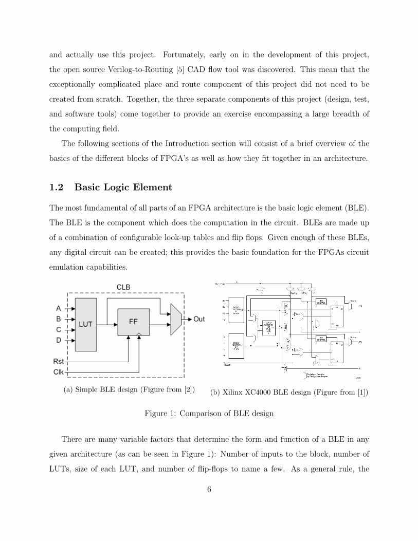
1.2 Basic Logic Element
The most fundamental of all parts of an FPGA architecture is the basic logic element (BLE).
The BLE is the component which does the computation in the circuit. BLEs are made up
of a combination of configurable look-up tables and flip flops. Given enough of these BLEs,
any digital circuit can be created; this provides the basic foundation for the FPGAs circuit
emulation capabilities.
(a) Simple BLE design (Figure from [2]) (b) Xilinx XC4000 BLE design (Figure from [1])
Figure 1: Comparison of BLE design
There are many variable factors that determine the form and function of a BLE in any
given architecture (as can be seen in Figure 1): Number of inputs to the block, number of
LUTs, size of each LUT, and number of flip-flops to name a few. As a general rule, the
6

more complicated the BLE, the less signals need to be routed by the global interconnect.
This makes logical sense seeing as when a circuit is broken into more sub-circuits (as needed
with a few input BLE) there are more nets connecting BLEs together. This increases the
minimum bus width of the interconnect fabric in order to achieve the same route-ability as
an architecture featuring a more complicated BLE design.
In opposition, a large BLE design with many LUTs and flip flops may reduce congestion
on the interconnect fabric but makes the architecture more prone to inefficient use of its logic
resources, since there may be a significant unused portion of each LUT in each complicated
BLE. Ultimately, the most efficient BLE design is dependant on the use case for the final
hardware, with general purpose FPGAs often using a combination of 2 4-LUTs paired with
a smaller 3-LUT and 2 flip flops, as in the Xilinx XC4000EX architecture (Figure 1b) [1].
This allows the routing software to use this BLE as 2 separate 4-LUT BLEs or one larger
5-LUT BLE, thereby partially circumventing the inefficiency problem.
1.3 Connection Box
Figure 2: 3 input 3 output connection box
7

The Connection Box (CB) is a unidirectional switching block allowing signals to enter
and exit the general fabric bus of the FPGA. A simple (fully-connected) CB design would
consist of each output pin from the module being connected to a mux which could select
from any of the inputs (or none of them). Another of way to implement this module would
be to have two buses of wires running perpendicular to each other on different layers of
silicon. These two buses would be connected at each crossing with a transistor which can
short the circuit between the two different bus domains as can be seen in Figure 2. Both
of these simple Connection Box designs allow any of the input pins to be directed to any
number of the output pins.
1.4 Logic Cluster
Figure 3: General logic cluster diagram (Figure from [6])
A strategy to put less stress on the fabric of the FPGA while also retaining a simple
BLE design is to use the concept of a Logic Cluster to introduce a separation in global
routing resources and local routing resources. A Logic Cluster is simply a group of BLEs
combined with a connection box (now referred to as an interconnect matrix) so that a more
8

complex operation can be performed without being routed through the general interconnect.
Usually, there are 4 to 16 BLEs per Logic Cluster [6] which all have their outputs connected
as inputs into the main interconnect matrix as well as out of the module (into the general
interconnect). This enables other BLEs in the same logic cluster to use those outputs,
enabling more complicated designs to be created without using global routing resources at
all (for the intermediate signals).
1.5 Switch Block
The switch block is fundamentally just as important as the BLE is to the basic FPGA
architecture. Combinations of this block create the entire FPGA routing scheme and allow
signals to be dynamically routed throughout the design so that any digital circuit can be
implemented. A switch block is generally designed as a bidirectional switch that acts as the
interchange for the intersection of 4 buses of the FPGA fabric. There are also unidirectional
switch blocks, although these designs require larger bus widths to achieve the same route-
ability in exchange for the simpler switch design.
Figure 4: Comparison of connection patterns of modern switch blocks (Figure from [4])
There are many different strategies to determine which bus wires are able to be connected
to each other as seen in Figure 4. The simplest of these is the disjoint connection pattern.
9

As the name suggests, this strategy creates separate routing domains from each wire in each
bus and once a signal is in one domain it is not able to be routed through any other domain.
For example, if 4 10-bit buses are using a disjoint switch block as an interchange, the first
wire in the top bus can only be connected to the first wire in the other 3 buses, not any of
the other wires. This does decrease route-ability due to having separate domains but is also
a very predictable and easily understandable strategy. Other strategies (such as the Wilson
or universal patterns) create several orders of magnitudes greater number of possible routes
to get from point to point and thus require much more complicated routing algorithms. The
main example of this point is that with a disjoint switch block based fabric, once a signal is
in the fabric it will always remain on the same track. This is not true for the other switch
patterns and allows for less assumptions to be made about track use throughout the fabric.
1.6 Input/Output Block
Figure 5: Xilinx XC4000 IO block (Figure from [1])
The IO block is another of the essential components of an FPGA, although its function
10
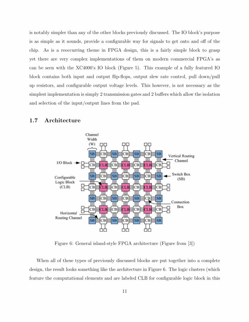
is notably simpler than any of the other blocks previously discussed. The IO block’s purpose
is as simple as it sounds, provide a configurable way for signals to get onto and off of the
chip. As is a reoccurring theme in FPGA design, this is a fairly simple block to grasp
yet there are very complex implementations of them on modern commercial FPGA’s as
can be seen with the XC4000’s IO block (Figure 5). This example of a fully featured IO
block contains both input and output flip-flops, output slew rate control, pull down/pull
up resistors, and configurable output voltage levels. This however, is not necessary as the
simplest implementation is simply 2 transmission gates and 2 buffers which allow the isolation
and selection of the input/output lines from the pad.
1.7 Architecture
Figure 6: General island-style FPGA architecture (Figure from [3])
When all of these types of previously discussed blocks are put together into a complete
design, the result looks something like the architecture in Figure 6. The logic clusters (which
feature the computational elements and are labeled CLB for configurable logic block in this
11
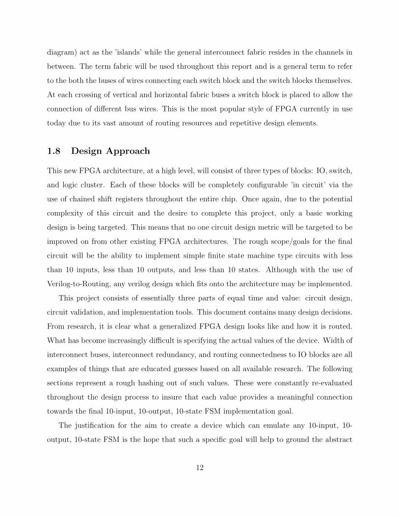
diagram) act as the ’islands’ while the general interconnect fabric resides in the channels in
between. The term fabric will be used throughout this report and is a general term to refer
to the both the buses of wires connecting each switch block and the switch blocks themselves.
At each crossing of vertical and horizontal fabric buses a switch block is placed to allow the
connection of different bus wires. This is the most popular style of FPGA currently in use
today due to its vast amount of routing resources and repetitive design elements.
1.8 Design Approach
This new FPGA architecture, at a high level, will consist of three types of blocks: IO, switch,
and logic cluster. Each of these blocks will be completely configurable ’in circuit’ via the
use of chained shift registers throughout the entire chip. Once again, due to the potential
complexity of this circuit and the desire to complete this project, only a basic working
design is being targeted. This means that no one circuit design metric will be targeted to be
improved on from other existing FPGA architectures. The rough scope/goals for the final
circuit will be the ability to implement simple finite state machine type circuits with less
than 10 inputs, less than 10 outputs, and less than 10 states. Although with the use of
Verilog-to-Routing, any verilog design which fits onto the architecture may be implemented.
This project consists of essentially three parts of equal time and value: circuit design,
circuit validation, and implementation tools. This document contains many design decisions.
From research, it is clear what a generalized FPGA design looks like and how it is routed.
What has become increasingly difficult is specifying the actual values of the device. Width of
interconnect buses, interconnect redundancy, and routing connectedness to IO blocks are all
examples of things that are educated guesses based on all available research. The following
sections represent a rough hashing out of such values. These were constantly re-evaluated
throughout the design process to insure that each value provides a meaningful connection
towards the final 10-input, 10-output, 10-state FSM implementation goal.
The justification for the aim to create a device which can emulate any 10-input, 10-
output, 10-state FSM is the hope that such a specific goal will help to ground the abstract
12

Figure 7: Basic finite state machine block diagram (Figure from [7])
nature of FPGA’s. With this goal in mind, design decision ’tiebreakers’ can be handled
more easily because the answer to the difficult question of deciding on important variables
is always ”Which value will give better results to the goal FSM circut?”. The basic setup
of this FSM type design can be seen in Figure 7 above. The FSM structure also provides
the use of storage elements without muddying the division between clock signals and data
signals. On real FPGA’s data signals can be used as global clock signals and fed into flip
flops where multiple clocks can be selected from. This would create additional complexity
vs a FSM targeted system where the next state is updated on each clock rising edge.
1.9 Report Organization
The following pages of the report will consist of the design sections followed by verification
and finally the conclusion. The design section will begin with the low level hardware specifi-
cation of the FPGA itself (Section 2) and move towards the software tools with each section
thereafter. The design section will be followed by Section 3 which will cover the integration
of the open source Verilog-to-Routing place and route tool into this project. The bitstream
generation tool will be discussed next in Section 4. After the three design sections, the
verification section (Section 5) will show the FPGA and toolset in action with a select set of
Verilog designs. Lastly, the conclusion will review the final results of the project, highlighting
some important points brought up in the design and verification sections.
13

2 Circuit Design
2.1 Architecture
Figure 8: Block diagram for new architecture
The design of this architecture attempts to mimic the well established island FPGA
architecture from Section 1.7. The specific internal block diagram for this project can be
seen in Figure 8, made up of 20 IO blocks, 5 switch blocks, 12 connection boxes, and 4 logic
clusters. The fabric of the FPGA is 10 wires wide represented by the thicker lines connecting
14

the switch blocks and connection boxes.
The general size of this architecture was decided based on the need for an architecture
which could be routed by hand if enough progress was not made on the place/route/bitstream
software tool set. This size is definitely limiting when attempting to implement general
verilog designs but is actually very helpful when working out and planning a configuration
for a gate-level diagram by hand which was done many times during the development process
to get a better understanding of how each block works together. In alignment with the
overarching goal for this circuit to implement the medium sized FSM, this design provides
the correct amount of IO’s and provides more than 5 times the required amount of state
storage. This gives much lenience to the HDL programmer to design state storage in less
efficient (but more logical) ways and leaves plenty of room to implement next state and
output conversion logic (Figure 7).
The design has 4 Banks of 5 IO blocks. The north and south blocks are biased towards
inputs as they can be routed to the input pins of a logic cluster by going through only a
single switch block. The east and west blocks are biased towards outputs as they can be
routed to from a logic cluster in one or less switch block connections. This decision attempts
to remove the necessity of the use of global routing resources by allowing a number of signals
in well designed circuits to avoid going through the center switch block (where each signal
can consume a maximum of 10% of the total global wires).
On an implementation note, the use of tri-state buses is prevalent throughout this Verilog
design as the entire FPGA fabric is based on the idea of configurable bidirectional buses
between each of the switches. From this use of tri-state comes additional complexity in
terms of creating the bitstream with defaults that ensure when a programmable multiplexer
is not configured from its default state (zero’s) that it does not drive the wire it is connected
to. This was accomplished with the creation of a high z line which is connected to each
non-interconnect matrix connection box’s zero bit input. This ensures that the hardware
design supports the idea of a default zero state. This idea is also carried over to the switch
block where any wire being driven with the default select bits (”00”) is connected to a high
15

z line.
Through debugging many undefined signal simulation errors it was found that this strat-
egy would not prove to be successful with the interconnect matrix. The problem was that
any high z wire which was an input into a look up table would cause the lut output to be
undefined (yes, even though the result would have been the same had that line been either
a 1 or a 0!). This default high z wire was replaced with a constant ground for intercon-
nect matrices. It is not clear whether this precaution would actually be necessary for a real
chip design since the wire would be forced to either a 1 or 0, although it was required for
simulation.
2.2 Programming Circuit
Figure 9: Block diagram for new architecture with programming order
As is required to achieve the design goals for this circuit, all of the settings for each
block are completely configurable through a snake of shift registers that runs throughout the
16

circuit (Figure 9). The programming order chosen was based on connecting spatially close
blocks. Originally, this was done with only clock and data wires. An additional enable wire
was added to both decrease the probability of the circuit being changed by noise during use,
and to more easily internally detect when the in-circuit programming was complete. Overall
there are 1480 configuration bits in one bitstream to specify an implemented design for this
architecture.
2.3 Basic Logic Element
Figure 10: Basic logic element circuit diagram
The basic logic element, as discussed in Section 1.2, is the computational center of the
FPGA, it contains the look up tables and the memory storage elements. The design of the
BLE block used in this project is very basic. The block design can be seen in Figure 10 and
the verilog code can be found here. The BLE contains 3 2-bit muxes, 1 16-bit mux, and 2 19-
bit shift registers, 16-bits of which are used in the 4-LUT. The remaining 3 bits are used to:
enable the feedback path from the flip flop to input A of the 4-LUT, enable the use of input
D as the enable input to the flip flop, and lastly to select the flip flop as output or the 4-LUT
as the output. This design will aid in simplicity of circuit verification and in implementation
routing. The addition of two sets of shift registers was discovered to be required during
simulation as the circuit would enter into invalid states while being programmed and cease
to continue simulating. To combat this problem, there are two banks of shift registers. The
first is used only while the device is being programmed (as told by the prog enable signal).
The second is only filled when the final control signals are in the programming shift registers
17

(falling edge of prog enable signal). In total, there are 19 configuration bits to fully specify
BLE functionality.
2.4 Connection Box
Figure 11: Circuit diagram of a programmable multiplexer
The connection box, as discussed in Section 1.3, is the way in which signals get onto
and out of the fabric buses of the FPGA. The connection box implementation is based on
the combination of many less complicated logic blocks called programmable multiplexers
(prog mux). A prog mux is simply a mux combined with a shift register which is in the
configuration chain of the FPGA. This enables the logic block to be connected to a number
of inputs in hardware but have the ultimate selection of which wire to drive to the output
done at programming time as part of the bitstream. A graphical representation of this block
can be seen in Figure 11.
Once the prog mux block is created, the design for a connection box is relatively simple
as described in Section 1.3. A prog mux is created for each output pin. The size (number
of select bits) of the prog mux is determined by taking the ceiling of the log base 2 of the
number of inputs. The use of Verilog parameters (as seen here and here) makes both the
connection box and the prog mux reusable throughout the rest of the HDL design.
There are 4 locations where the connection box block is used: getting inputs from the IO
blocks to the fabric, getting outputs from the fabric to the IO blocks, getting logic cluster
18

outputs into the fabric, and as an interconnect matrix inside of a logic cluster. Respectively
these implementations require 30 bits, 20 bits, 30 bits, and 80 bits to configure.
2.5 Logic Cluster
Figure 12: Logic cluster diagram (including output connection box)
The logic cluster is a combination of a connection box and multiple basic logic elements as
discussed in Section 1.4. The number of BLE’s was chosen to be 5. This was a value that
seemed reasonable in regards to how much total memory and logic resources it produced.
It also allowed the use of 16 input prog muxes (instead of 32 input) with a 10-bit fabric
bus. The choice of 6 BLE’s also would have allowed the use of 16 input prog muxes but
5 BLE’s times 4 logic clusters already provided more than enough resources to achieve the
FSM goal. A complete logic cluster takes 175 bits to program (this number is the sum of all
configuration bits of the sub blocks as the logic cluster itself has no additional configuration
capabilities).
19

The graphic in Figure 12 is a good way to represent the entire view of a logic cluster.
This diagram was printed out and used to walk though the place and route problem in
complete detail. Lines can be drawn in both connection boxes to show connections to and
from BLE’s while gate level diagrams can be drawn in each BLE block and then translated
into the look up table equivalent. This process was done many times during development to
ensure understanding of how everything fit together.
2.6 Switch Block
The switch block design uses the disjoint connection pattern to create the simplest possible
fabric structure to connect each of the individual buses in the FPGA fabric. The block has
4 10-bit wide bus connections which are all bidirectional. The internal makeup of the switch
block is (like the connection box) just made up of many prog muxes driving the output
pins of each pin of the bus connections with an additional connection for not driving the
output (High Z). To fully specify the configuration of a switch block 80 bits of information
are required.
2.7 Input/Output Block
The IO block was influenced by the complicated Xilinx model referenced in Figure 5 but
reduced significantly. It consists of the minimum setup (a few tri-state drivers) plus pull
up/down resistors with pass transistor enables, and the shift registers required to program
it. The pull-up and pull-down resistors however, are not applicable when dealing with this
Verilog implementation and static digital simulation. Due to the simplicity of this block,
only 3 bits are required to program the IO block.
20

3 Verilog-to-Routing
3.1 Introduction
Verilog-to-Routing (VTR) [5] is the premiere open source FPGA CAD flow for FPGA aca-
demic research. This tool allows any FPGA architecture to be worked on with the use of
its architecture description language to specify every detail about the architecture. The
fact that this tool was discovered (through extensive background research) aided the project
tremendously due to how many complex algorithms could be left to VTR to handle. VTR
is comprised of 3 separate tools: Odin, ABC, and VPR. Odin is used to synthesize and
elaborate Verilog files into BLIF netlist files which can be implemented on the specified ar-
chitecture. The next tool executed is ABC which optimizes the netlist. Versatile Place and
Route (VPR) is the final step in the flow which takes the netlist produced in the previous
step and places the individual groups of logic and routes the nets on the architecture. VPR
also provides a graphical representation to view how the circuit is implemented on the device.
While the original goal of this project was to create an FPGA from scratch (including
the software tools) the use of VTR was deemed to be a good decision for two main reasons.
First, VTR is a sort of academic standard and provides all sorts of additional features (not
used in this project) to help benchmark and compare FPGA architectures. Therefore, this
was seen as a good opportunity to learn a new toolset in a hands-on manor for possible
future projects in this area of study. Second, the algorithms that VTR handles are complex
(NP-Hard) and also creates the opportunity to implement Verilog designs instead of hand
produced netlists and logic. Specifically the VPR tool provides a way to avoid writing a new
place and route algorithm which would have been passable with this size of architecture but
would have struggled with any increase in size (as a good place and route algorithm could
be a whole senior project on its own).
21

3.2 Architecture Description
Figure 13: VTR parse and stylized rendering of new architecture (programming signals
omitted)
In order to integrate with the VTR CAD flow both a Verilog file and an architecture descrip-
tion file must be provided. The Verilog is straightforward and marks a huge improvement
over hand drawing circuits and feeding them into a hand-written tool, but the architecture
description language is a whole other concept to grasp. This language uses an XML format
to specify every possible variable within an architecture including: setup-hold times, switch
block connection strategy, block locations, BLE size, and much more. For this project, all
timing information was deemed to be out of scope so there are placeholder times, resistances,
22

and capacitances where real values should be (VTR did not accept the concept of an ’ideal’
FPGA and refused to route it). This file can be found here and it produces the graphical
representation found in Figure 13.
As can be seen in Figure 13, there are slight differences in how VTR perceives this
architecture vs how it was designed (Figure 8). These differences are mainly present in the
fabric and switch block layout and are due to the lack of granularity control in specifying
the location of the fabric and switch blocks. The VTR tool makes the assumption that the
architecture being specified is a regular island type architecture (which has a very regular
fabric structure) and spends much more effort in understanding the various clb’s (complex
logic blocks: IO, logic cluster, BLE). This difference is entirely cosmetic as there is still a
strict equivalence between the channels from the designed to the interpreted architectures
which is important for generating the bitstream.
Another notable diversion from the design specified is that many of the auxiliary control
signals for the BLE implementation are missing from the architecture specification file (in-
ternal feedback and flip flop enable) due to being unable specify them in the architecture
file. These features are still in the HDL implementation of the device and still accessible via
hand programming although they will be unknown (and unusable) to the VTR flow.
3.3 Example
The main example that will be used in this report is a simple sequence detector circuit
with an output bus that drives a seven-segment display with the current state. This is a
classic example of a FSM type of design although it only has 3 inputs (including clock) and
7 outputs. The design recognizes the 9-bit long sequence ”101100100” which takes 9 states
(one for each bit of the sequence) and one additional state for an initial zero. This can be
seen in more detail in the code listing for this example (found here). Figure 14 showcases this
example circuit implemented on the new architecture. Some notable observations include
how the concept of input and output biased IO banks are not taken into account. Also it
is surprising to see 100% BLE utilization within the architecture with this design. Usually,
23

routing resources are the main obstacle in the implementation onto an FPGA. Anywhere
from 85%-90% logic utilization is usually where commercial place and route algorithms begin
to struggle to successfully route designs.
Figure 14: VTR rendering of sequence detector implementation
24

4 Bitstream Generation
The main software tool which was produced for this project was the bitstream generation
tool. The 2 objectives for this piece of software are: parse and make sense of the VTR output
files, and output this virtual representation of the implemented design into a bitstream which
will program the device. The first of these objectives proved to be a rigorous exercise in
reading sparse documentation.
The first of these output files is the Berkeley Logic Interchange Format (BLIF). This
file describes (at a high level) what the inputs, outputs, and how each of the outputs are
calculated. This file is created with the overall architecture LUT size in mind so the logic
descriptions can be directly parsed as LUT settings. It also specifies which of the BLE’s flip
flops are used.
The next file to be parsed is the place file (.place). This file is the simplest to be parsed
and only contains a description of what internal names (used in the net file) correspond
to which coordinates within the architecture. Once the coordinates are known the type of
block can be determined. This file also allows a quick way to see where each of the IO’s were
placed (bank [NESW], subblock[0-4]) for easy reading off for testbench setup.
After the place file, the route file (.route) is parsed. For each net that uses global routing
resources an entry is created in this file to describe what the source, sink and the switch
path which is taken to connect those points together (switches, tracks used, etc).
The final and most extensive output file that is parsed is the .net file. This is a XML
based file which enumerates every non-switch block in the architecture and maps the im-
plementation details of each of them. The net file provides the glue which allows all of the
previously parsed information to be combined and put into a virtual representation of the
architecture, like which IO’s are inputs or outputs, which logic cluster each net’s LUT is
placed, and which signals to send to which BLE’s.
During the parsing of the net file, an ’FPGA’ object is created and filled out with the
various settings described in the VTR output files. Once the parsing is complete, the FPGA
object is prompted to print out all of the settings it contains in a valid bitstream.
25

This software was written using Java. This decision was made due to it being somewhat
similar to C but also providing much more extensive library support for all of the string
and XML parsing tasks required. This decision kept the line count reasonable while still
providing a lot of functionality.
26

5 Circuit Verification
Verification/bug fixing this circuit was a very difficult task due to the sheer number of signals
as well as the overall complexity of the circuit. Debugging and verifying this circuit consisted
in the repetition of (1) identifying there was an error (2) identifying where the incorrect signal
originated (2) identifying the source of the incorrect signal (3) figuring out why an incorrect
configuration was produced and fixing the parsing tool to handle it in the future. This
process was made time consuming because of the difficulty in tracking signals through the
architecture and comparing that to where they were supposed to be. This required the
simultaneous use of Vivado (testbench simulation), IntelliJ (Bitstream Java development),
and the interactive VTR graphical tool (to see what the correct settings should be) in order
to identify and fix bugs.
The next three subsections will provide simulation results for three different Verilog
designs implemented on the new FPGA architecture. In order to run these simulations,
first, a Verilog design was created (Example here). Then, this Verilog file was run through
the VTR toolset which outputs the files discussed in the previous section (.net, .place, .blif,
.route). These output files are then used as inputs for the bitstream generation tool which
then outputs a 1480-bit long bitstream. This bitstream is then copied into a testbench
that instantiates the Verilog FPGA architecture and connects the inputs and outputs to the
design as seen in the next 3 sections.
5.1 Adder
This adder circuit is one of the simplest designs that an FPGA can implement which still
requires a moderate amount of intermediate nets to route. As seen in Figure 15 there is
an ’out’ signal as well as a ’correct’ signal. The out signal comes directly from the Verilog
FPGA while the ’correct’ signal is computed by the simulator. The programming signals are
omitted due to length and lack of clarity added (a zoomed out screenshot of a design being
programmed can be seen in Section 5.3). Notice all test cases showing equal results between
the computed output and the correct output.
27

Figure 15: Output of 4-bit adder testbench
5.2 Register
The next example circuit is a simple set-clear register to demonstrate the use of memory
elements in the architecture. As with the previous adder example, both output and correct
signals are provided for easy verification.
Figure 16: Output of register testbench
5.3 Sequence Detector
The testbench for this circuit uses the same FSM design from Section 3.3. As can be seen
in the testbench code (found here) the actual FSM Verilog file was, in addition to being
implemented on the FPGA, also instantiated in the simulator so that the correct output
could be known easily. In addition, a logic block is included in the test bench to convert the
28

seven segment display formatted output into a regular number representation.
Figure 17: Programming the sequence detector testbench
The following timing diagrams were generated from the Vivado simulator, the program-
ming signals are shown in Figure 17 at a very high level. Figure 18 shows the state machine
advance through all of its internal states as the desired sequence is passed into the design
(”101100100”) one by one. The ”led out” signal is the output from the FPGA while the
”correct” signal is the simulation software’s interpretation of the FSM design. The ”state”
signal is the converted ”led out” value into a regular number. It can be seen clearly that the
FPGA output is always consistent with the correct output.
Figure 18: Output of sequence detector testbench
Next an incorrect sequence will be fed into the state machine in Figure 19. ”100” are the
first three bits fed into the FSM. This will cause the design to advance to state 2 (on the
2nd bit) but then fall to state zero after reading the 3rd bit due to it being incorrect.
29

Figure 19: Output of sequence detector testbench
The next simulation shows the bits ”1011011001000” being fed into the FSM. This causes
the behavior of advancing from state 1 to 5 and then falling back to 3 before advancing to
state 9. This happens due to the error in state 5. The next bit should be a 0, but a 1 is
given. Instead of going back to state 1 however, the last 3 bits entered match with state
3 (which represents the pattern ”101”). The next bits are then entered correctly until the
sequence is matched.
Figure 20: Output of sequence detector testbench
The final simulation shows the use of the reset input. The correct sequence is fed into
the FSM and before it can advance to the 6th state the reset pin is set to 1. Notice that the
correct output and the FPGA output diverge from the reset going high until the next rising
edge of the clock. This is due to the reset being specified as asynchronous in the Verilog
design, while the FPGA architecture is unable to implement such constructs. All flip flops
in any implemented designs are tied to the same global clock line.
30

Figure 21: Output of sequence detector testbench
31

6 Conclusion
Overall, this project was a success in spirit but slightly missed the stated goal of creating a
10-input 10-output 10-state capable FPGA architecture. The main reason that this project
fell slightly short is that the FSM target really needed a contrived example design to meet
the 10 input, 10 output requirements as FSM designs typically rely on smaller amounts of
inputs and outputs. This was partially overcome through the sequence detector example
due to the internal state being converted to a seven segment display format which occupied
more output pins. Still this design fell short of being able to implement an FSM with the
10-inputs and 10-outputs originally desired.
This small failure however, does not truly impact the usability of the design as the
majority of 10-state FSM’s will not require that many IO’s. This points to a small design
flaw in which the ratio of logic resources to IO’s is not optimal, however future designers
should be weary of decreasing the number IO’s too much as it could have the impact of
reducing the routeability of the architecture due to decreasing the number of IO pins in
desirable areas and therefore increasing the need for global routing resources.
The next reason that this project fell slightly short of it’s goals is that the FSM design
hoping to be implemented onto this architecture needs to be manipulated and ”worked”
in order to fit in the architecture. This can be seen by the fact that the sequence decoder
example utilized 100% of available logic resources and two fabric buses above 80% of available
track resources. In fact, just switching the desired pattern from ”101100100” to ”101100101”
caused the design to be unroutable. This means that the desired FSM design size has a
possibility of fitting onto this architecture, but there is a large subset of designs which have
10 states which will not fit on this architecture.
This utilization difficulty is caused to a substantial degree by the VTR place and route
algorithm. As pointed out in the VTR section, upon inspection of the implemented sequence
detector design, many of the IO blocks have not been placed in ideal locations. Inputs/Out-
puts seem to be placed in a somewhat random fashion, with little regard to the design’s IO
biases. It was not uncommon to see an output from the NE logic cluster be routed all the
32

way across the chip to the west IO bank. This is likely due to the general purpose nature of
the algorithm where a more specific place and route algorithm would have performed better
on this architecture.
Aside from these two slight failures, the rest of the project went successfully. The ability
to implement a select group of medium sized FSM designs onto a completely new FPGA
architecture designed in Verilog with the ability to program the device ’in-circuit’ with a
custom bitstream generation tool integrated with the academic standard of place route tools
should not be understated.
33

References
[1] The xilinx field programmable gate array series. Available at http://mazsola.iit.
uni-miskolc.hu/cae/docs/pld1.en.html.
[2] Programmable logic/fpgas, Nov 2007.
[3] Umer Farooq, Zied Marrakchi, and Habib Mehrez. Tree-based heterogeneous FPGA ar-
chitectures: application specific exploration and optimization. Springer, 2012.
[4] Guy Lemieux and David Lewis. Checkerboard switch block topologies for routing diver-
sity, 2002.
[5] Jason Luu, Jeff Goeders, Michael Wainberg, Andrew Somerville, Thien Yu, Konstantin
Nasartschuk, Miad Nasr, Sen Wang, Tim Liu, Norrudin Ahmed, Kenneth B. Kent, Jason
Anderson, Jonathan Rose, and Vaughn Betz. VTR 7.0: Next Generation Architecture
and CAD System for FPGAs. ACM Trans. Reconfigurable Technol. Syst., 7(2):6:1–6:30,
June 2014.
[6] Muhammad Imran. Masud. Fpga routing structures: a novel switch block and de-
populated interconnect matrix architectures. Master’s thesis, The University of British
Columbia, 1999.
[7] David Williams. Implementing a finite state machine in vhdl, Dec 2015.
34

7 Appendix
7.1 Github
The github project can be found at this URL: https://github.com/JosephPrachar/fpga
35
Recommended