Power Integrations
5245 Hellyer Avenue, San Jose, CA 95138 USA. Tel: +1 408 414 9200 Fax: +1 408 414 9201
www.powerint.com
Title Reference Design Report for a 6 W Constant Voltage (CV) Adapter Using LNK625PG
Specification 90 – 265 VAC Input; 5 V, 1.2 A Output
Application Low-Cost Charger or Adapter
Author Applications Engineering Department
Document Number
RDR-201
Date November 11, 2008
Revision 1.5
Summary and Features
• Eliminates optocoupler and all secondary side control circuitry
• EcoSmart® – Easily meets all existing and proposed international energy efficiency standards – China (CECP) / EISA / Energy STAR / European Commission
• ON/OFF control provides constant efficiency event at very light loads
• No-load consumption <100 mW at 265 VAC
• Meets ENERGY STAR 2.0 active mode efficiency
• 76 % vs 70 % requirement at board
• 73 % vs 70 % requirement at end of 6 ft, 315 mΩ output cable
• Ultra-low leakage current: <5 µA at 265 VAC input (no Y capacitor required)
• Over-temperature protection – tight tolerance (±5%) with hysteretic recovery for safe PCB temperatures under all conditions
• Auto-restart output short circuit and open-loop protection
• Easy compliance to EN550022 and CISPR-22 Class B EMI standards
• Green package: halogen free and RoHS compliant PATENT INFORMATION
The products and applications illustrated herein (including transformer construction and circuits external to the products) may be covered
by one or more U.S. and foreign patents, or potentially by pending U.S. and foreign patent applications assigned to Power Integrations. A
complete list of Power Integrations' patents may be found at www.powerint.com. Power Integrations grants its customers a license under
certain patent rights as set forth at <http://www.powerint.com/ip.htm>. .

RDR-201 6 W LinkSwitch-CV Adapter 11-Nov-08
Page 2 of 32
Power Integrations Tel: +1 408 414 9200 Fax: +1 408 414 9201 www.powerint.com
Table of Contents 1 Introduction.................................................................................................................3
2 Power Supply Specification ........................................................................................4
3 Schematic...................................................................................................................5
4 Circuit Description ......................................................................................................6
4.1 Input and EMI Filtering ........................................................................................6
4.2 LinkSwitch-CV Device .........................................................................................6
4.3 Primary Circuit .....................................................................................................6
4.4 Output Rectification .............................................................................................7
4.5 Feedback Winding...............................................................................................7
5 PCB Layout ................................................................................................................8
6 Bill of Materials ...........................................................................................................9
7 Transformer Specification.........................................................................................10
7.1 Electrical Diagram .............................................................................................10
7.2 Electrical Specifications.....................................................................................10
7.3 Materials............................................................................................................10
7.4 Transformer Build Diagram ...............................................................................11
7.5 Transformer Construction..................................................................................11
8 Transformer Spreadsheets.......................................................................................12
9 Performance Data ....................................................................................................15
9.1 Active Mode Efficiency ......................................................................................15
9.2 Energy Efficiency Requirements .......................................................................16
9.2.1 USA Energy Independence and Security Act 2007....................................17
9.2.2 ENERGY STAR EPS Version 2.0 ..............................................................18
9.3 No-load Input Power..........................................................................................19
9.4 Regulation .........................................................................................................19
9.4.1 Load ...........................................................................................................19
9.4.2 Line ............................................................................................................20
10 Thermal Performance ...........................................................................................21
11 Waveforms............................................................................................................22
11.1 Drain Voltage and Current, Normal Operation...................................................22
11.2 Output Voltage Start-up Profile..........................................................................23
11.3 Drain Voltage and Current Start-up Profile ........................................................23
11.4 Load Transient Response (75% to 100% Load Step) .......................................23
11.5 Output Ripple Measurements............................................................................25
11.5.1 Ripple Measurement Technique ................................................................25
11.5.2 Measurement Results ................................................................................26
12 Line Surge.............................................................................................................27
13 Conducted EMI .....................................................................................................28
14 Revision History ....................................................................................................29
Important Note: Although this board is designed to satisfy safety isolation requirements, the engineering prototype has not been agency approved. Therefore, all testing should be performed using an isolation transformer to provide the AC input to the prototype board.
11-Nov-08 RDR-201 6 W LinkSwitch-CV Adapter
Page 3 of 32
Power Integrations Tel: +1 408 414 9200 Fax: +1 408 414 9201
www.powerint.com
1 Introduction
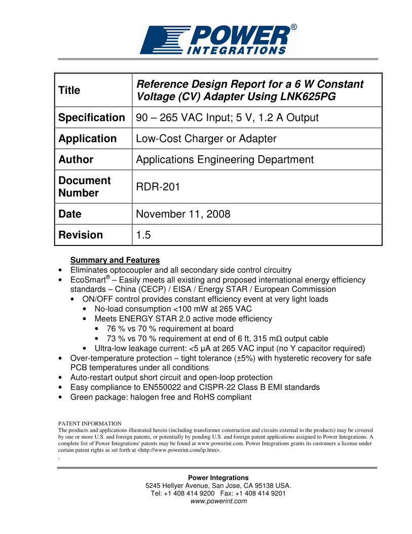
This document is an engineering report describing a universal input, 5 V, 6 W output Flyback power supply. This reference design is based on the LinkSwitch-CV family of devices and utilizes the LNK625PG. The document contains the power supply specification, schematic, bill of materials, transformer documentation, printed circuit layout, and performance data.
Figure 1 – Populated Circuit Board Photograph.
RDR-201 6 W LinkSwitch-CV Adapter 11-Nov-08
Page 4 of 32
Power Integrations Tel: +1 408 414 9200 Fax: +1 408 414 9201 www.powerint.com
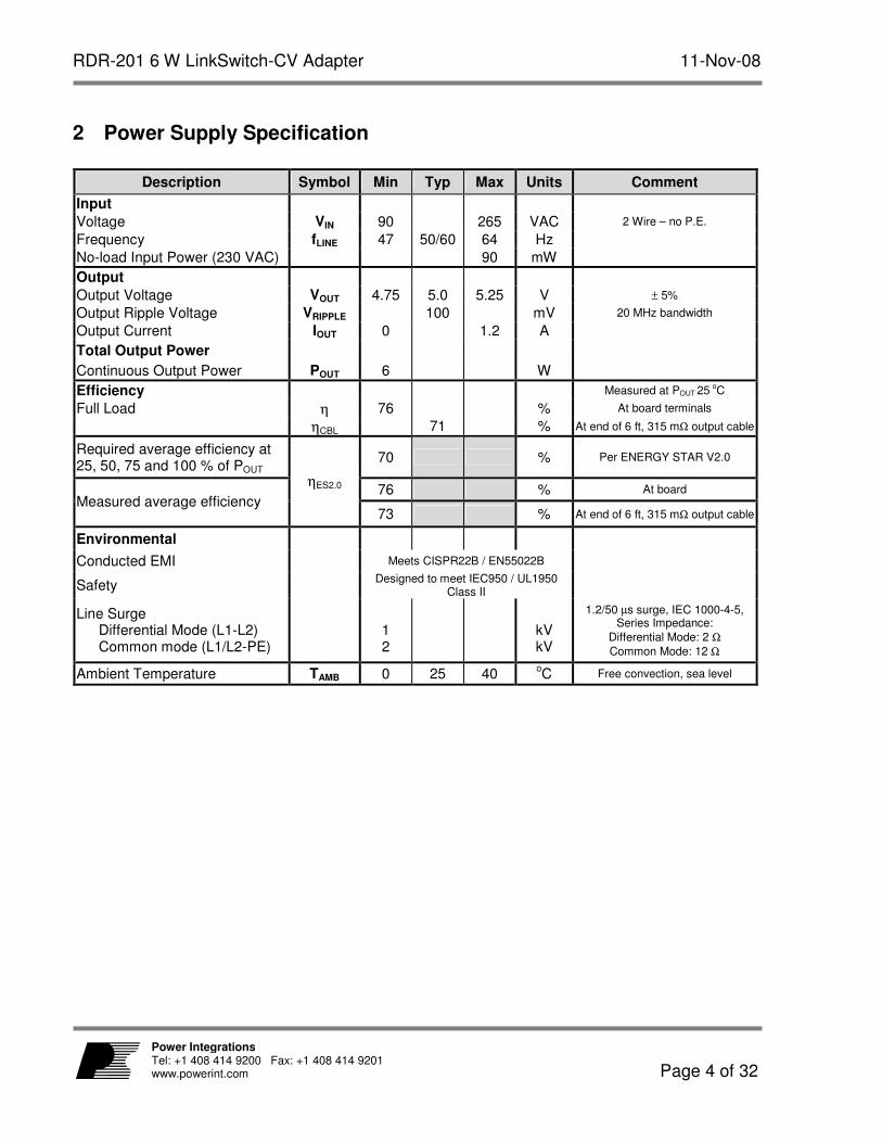
2 Power Supply Specification
Description Symbol Min Typ Max Units Comment
Input
Voltage VIN 90 265 VAC 2 Wire – no P.E.
Frequency fLINE 47 50/60 64 Hz
No-load Input Power (230 VAC) 90 mW
Output
Output Voltage VOUT 4.75 5.0 5.25 V ± 5%
Output Ripple Voltage VRIPPLE 100 mV 20 MHz bandwidth
Output Current IOUT 0 1.2 A
Total Output Power
Continuous Output Power POUT 6 W
Efficiency Measured at POUT 25 o
C
Full Load η 76 % At board terminals
ηCBL 71 % At end of 6 ft, 315 mΩ output cable
Required average efficiency at 25, 50, 75 and 100 % of POUT
70 % Per ENERGY STAR V2.0
76 % At board Measured average efficiency
ηES2.0
73 % At end of 6 ft, 315 mΩ output cable
Environmental
Conducted EMI Meets CISPR22B / EN55022B
Safety Designed to meet IEC950 / UL1950
Class II
Line Surge Differential Mode (L1-L2) Common mode (L1/L2-PE)
1 2
kV kV
1.2/50 µs surge, IEC 1000-4-5, Series Impedance:
Differential Mode: 2 Ω
Common Mode: 12 Ω
Ambient Temperature TAMB 0 25 40 oC Free convection, sea level
11-Nov-08 RDR-201 6 W LinkSwitch-CV Adapter
Page 5 of 32
Power Integrations Tel: +1 408 414 9200 Fax: +1 408 414 9201
www.powerint.com
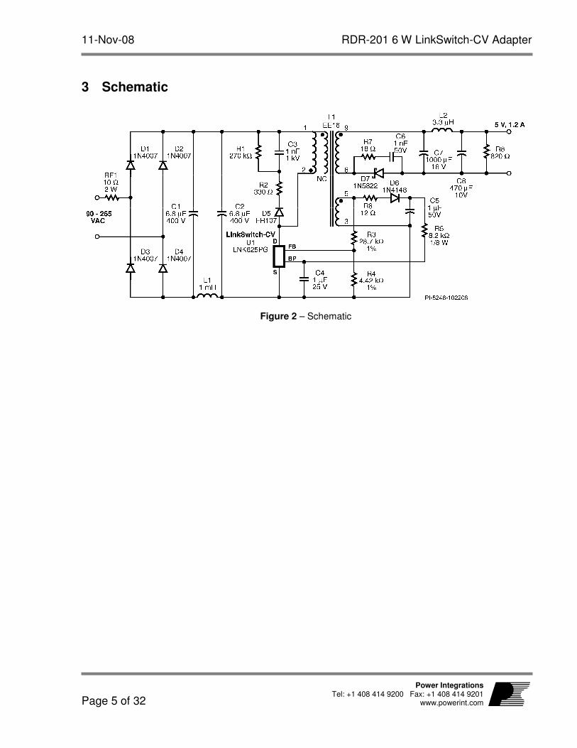
3 Schematic
Figure 2 – Schematic
RDR-201 6 W LinkSwitch-CV Adapter 11-Nov-08
Page 6 of 32
Power Integrations Tel: +1 408 414 9200 Fax: +1 408 414 9201 www.powerint.com
4 Circuit Description
The schematic in Figure 2 shows an adapter design using the LNK625PG that provides very tight constant voltage (CV) performance. The circuit is designed to operate from 90 VAC to 265 VAC input, with an output voltage of 5 V providing a maximum load current of 1.2 A. It consumes very little standby power and uses no Y-Capacitor to meet stringent EMI requirements. The adapter also meets and exceeds both CEC and Energy Star 2.0 regulations.
4.1 Input and EMI Filtering
Diodes D1 through D4 form a full wave rectifier. The rectified DC is then filtered by capacitors C1 and C2. Inductor L1 forms a pi (π) filter with capacitors C1 and C2 which helps to reduce differential EMI noise. This filtering, together with the integrated switching frequency jitter provided in U1 and transformer E-Shield techniques, provide a generous EMI margin without the need for a Y capacitor across the primary and secondary windings of transformer T1.
4.2 LinkSwitch-CV Device
The LinkSwitch-CV family of devices has been developed to cost effectively replace all existing solutions in low power adapter applications. It is optimized for constant voltage (CV) adapter applications while using minimal external parts including the complete elimination of the optocoupler and shunt regulator. The LNK625PG monolithically integrates the 700 V power MOSFET switch and controller, which consists of an oscillator, feedback (sense and logic) circuit, 6 V regulator, BYPASS pin programming functions, over-temperature protection, frequency jittering, current limit circuit and leading-edge blanking. The LNK625PG also provides a sophisticated range of protection features including auto-restart for control loop component open/short circuit faults and output short circuit conditions. The use of a low auto-restart on time reduces the power delivered by more than 95 % for output short circuits and control loop faults. Accurate hysteretic thermal shutdown ensures safe average PCB temperatures under all conditions. Extended creepage distance between high and low voltage pins prevent arcing and helps meet safety requirements. LinkSwitch-CV also can be used without a bias winding as the IC is completely self biased.
4.3 Primary Circuit
During U1’s on time current flows through the primary winding of transformer T1 and stores energy in its magnetic field. During U1’s off time, the energy stored in the transformer is transferred to the secondary side, delivering current to both the output capacitors and the load.
11-Nov-08 RDR-201 6 W LinkSwitch-CV Adapter
Page 7 of 32
Power Integrations Tel: +1 408 414 9200 Fax: +1 408 414 9201
www.powerint.com
The clamp circuit formed by resistors R1 and R2 along with blocking diode D5 and capacitor C3 ensures that the drain node voltage is well below the 700 V rating of the internal MOSFET of U1. The clamp circuit is also carefully designed to reduce and dampen any oscillation present in the voltage spike caused by the transformer’s leakage inductance.
4.4 Output Rectification
The secondary output is rectified by diode D7 which is placed in the return leg to help reduce EMI and simplify the transformer construction. An RC snubber circuit composed of resistor R7 and capacitor C6 is placed across the output diode to also reduce high frequency EMI. A stable output voltage is maintained by capacitor C7. Inductor L2 and capacitor C8 form an LC post filter which helps to attenuate switching noise and reduces output ripple. Resistor R8 is a preload resistor whose value has been empirically chosen to provide the best possible regulation at light loads without significantly affecting no-load input power or efficiency.
4.5 Feedback Winding
LinkSwitch-CV eliminates the need for an optocoupler for tight output voltage regulation, as good as ±5 %, through the use of a feedback winding. The feedback (FB) pin voltage, which is derived from the voltage divider formed by resistors R3 and R4, is sampled approximately 2.5 µs after U1’s internal MOSFET turns off. Based upon this information the device regulates the output voltage. The feedback winding was also designed with more turns than necessary so that it may act as a bias winding. The winding provides bias current to U1 through the bypass pin (BP) and reduces the input power consumption during light loads and no-load conditions. Resistor R6 helps to dampen out any ringing present on the feedback winding and ensures that the waveform at the FB pin at 2.5 us is free from any ringing. Capacitor C5 provides a stable bias voltage while resistor R5 is chosen to supply the necessary BP pin current. Capacitor C4 is the BP pin capacitor and should be placed as close as possible to the BP pin and source pins of the device.
RDR-201 6 W LinkSwitch-CV Adapter 11-Nov-08
Page 8 of 32
Power Integrations Tel: +1 408 414 9200 Fax: +1 408 414 9201 www.powerint.com
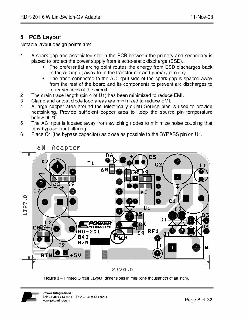
5 PCB Layout
Notable layout design points are: 1 A spark gap and associated slot in the PCB between the primary and secondary is
placed to protect the power supply from electro-static discharge (ESD).
• The preferential arcing point routes the energy from ESD discharges back to the AC input, away from the transformer and primary circuitry.
• The trace connected to the AC input side of the spark gap is spaced away from the rest of the board and its components to prevent arc discharges to other sections of the circuit.
2 The drain trace length (pin 4 of U1) has been minimized to reduce EMI. 3 Clamp and output diode loop areas are minimized to reduce EMI. 4 A large copper area around the (electrically quiet) Source pins is used to provide
heatsinking. Provide sufficient copper area to keep the source pin temperature below 90 ºC.
5 The AC input is located away from switching nodes to minimize noise coupling that may bypass input filtering.
6 Place C4 (the bypass capacitor) as close as possible to the BYPASS pin on U1.
Figure 3 – Printed Circuit Layout, dimensions in mils (one thousandth of an inch).
11-Nov-08 RDR-201 6 W LinkSwitch-CV Adapter
Page 9 of 32
Power Integrations Tel: +1 408 414 9200 Fax: +1 408 414 9201
www.powerint.com
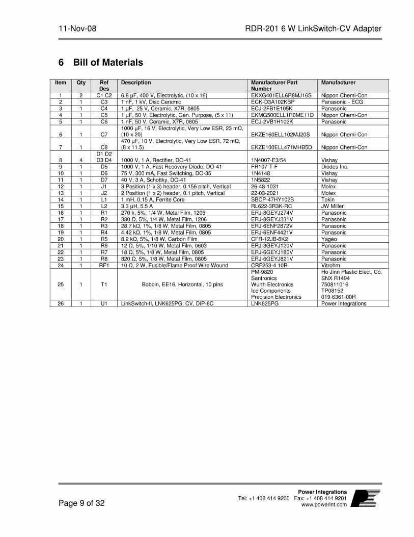
6 Bill of Materials
Item Qty Ref
Des Description Manufacturer Part
Number Manufacturer
1 2 C1 C2 6.8 µF, 400 V, Electrolytic, (10 x 16) EKXG401ELL6R8MJ16S Nippon Chemi-Con 2 1 C3 1 nF, 1 kV, Disc Ceramic ECK-D3A102KBP Panasonic - ECG
3 1 C4 1 µF, 25 V, Ceramic, X7R, 0805 ECJ-2FB1E105K Panasonic
4 1 C5 1 µF, 50 V, Electrolytic, Gen. Purpose, (5 x 11) EKMG500ELL1R0ME11D Nippon Chemi-Con
5 1 C6 1 nF, 50 V, Ceramic, X7R, 0805 ECJ-2VB1H102K Panasonic
6 1 C7 1000 µF, 16 V, Electrolytic, Very Low ESR, 23 mΩ, (10 x 20) EKZE160ELL102MJ20S Nippon Chemi-Con
7 1 C8 470 µF, 10 V, Electrolytic, Very Low ESR, 72 mΩ, (8 x 11.5) EKZE100ELL471MHB5D Nippon Chemi-Con
8 4 D1 D2 D3 D4 1000 V, 1 A, Rectifier, DO-41 1N4007-E3/54 Vishay
9 1 D5 1000 V, 1 A, Fast Recovery Diode, DO-41 FR107-T-F Diodes Inc.
10 1 D6 75 V, 300 mA, Fast Switching, DO-35 1N4148 Vishay
11 1 D7 40 V, 3 A, Schottky, DO-41 1N5822 Vishay
12 1 J1 3 Position (1 x 3) header, 0.156 pitch, Vertical 26-48-1031 Molex
13 1 J2 2 Position (1 x 2) header, 0.1 pitch, Vertical 22-03-2021 Molex 14 1 L1 1 mH, 0.15 A, Ferrite Core SBCP-47HY102B Tokin
15 1 L2 3.3 µH, 5.5 A RL622-3R3K-RC JW Miller
16 1 R1 270 k, 5%, 1/4 W, Metal Film, 1206 ERJ-8GEYJ274V Panasonic
17 1 R2 330 Ω, 5%, 1/4 W, Metal Film, 1206 ERJ-8GEYJ331V Panasonic
18 1 R3 28.7 kΩ, 1%, 1/8 W, Metal Film, 0805 ERJ-6ENF2872V Panasonic 19 1 R4 4.42 kΩ, 1%, 1/8 W, Metal Film, 0805 ERJ-6ENF4421V Panasonic
20 1 R5 8.2 kΩ, 5%, 1/8 W, Carbon Film CFR-12JB-8K2 Yageo
21 1 R6 12 Ω, 5%, 1/10 W, Metal Film, 0603 ERJ-3GEYJ120V Panasonic
22 1 R7 18 Ω, 5%, 1/8 W, Metal Film, 0805 ERJ-6GEYJ180V Panasonic
23 1 R8 820 Ω, 5%, 1/8 W, Metal Film, 0805 ERJ-6GEYJ821V Panasonic
24 1 RF1 10 Ω, 2 W, Fusible/Flame Proof Wire Wound CRF253-4 10R Vitrohm
25 1 T1 Bobbin, EE16, Horizontal, 10 pins
PM-9820 Santronics Wurth Electronics Ice Components Precision Electronics
Ho Jinn Plastic Elect. Co. SNX R1494 750811016 TP08152 019-6361-00R
26 1 U1 LinkSwitch-II, LNK625PG, CV, DIP-8C LNK625PG Power Integrations
RDR-201 6 W LinkSwitch-CV Adapter 11-Nov-08
Page 10 of 32
Power Integrations Tel: +1 408 414 9200 Fax: +1 408 414 9201 www.powerint.com
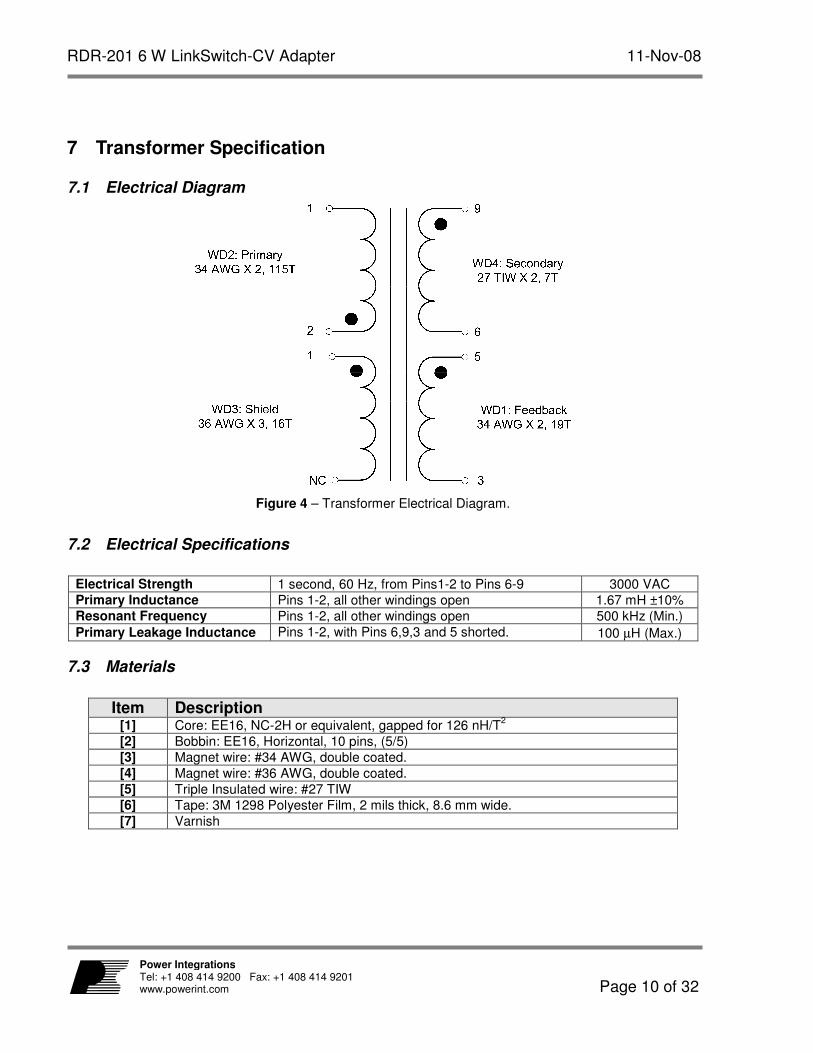
7 Transformer Specification
7.1 Electrical Diagram
Figure 4 – Transformer Electrical Diagram.
7.2 Electrical Specifications
Electrical Strength 1 second, 60 Hz, from Pins1-2 to Pins 6-9 3000 VAC Primary Inductance Pins 1-2, all other windings open 1.67 mH ±10% Resonant Frequency Pins 1-2, all other windings open 500 kHz (Min.)
Primary Leakage Inductance Pins 1-2, with Pins 6,9,3 and 5 shorted. 100 µH (Max.)
7.3 Materials
Item Description
[1] Core: EE16, NC-2H or equivalent, gapped for 126 nH/T2
[2] Bobbin: EE16, Horizontal, 10 pins, (5/5) [3] Magnet wire: #34 AWG, double coated. [4] Magnet wire: #36 AWG, double coated. [5] Triple Insulated wire: #27 TIW [6] Tape: 3M 1298 Polyester Film, 2 mils thick, 8.6 mm wide. [7] Varnish
11-Nov-08 RDR-201 6 W LinkSwitch-CV Adapter
Page 11 of 32
Power Integrations Tel: +1 408 414 9200 Fax: +1 408 414 9201
www.powerint.com
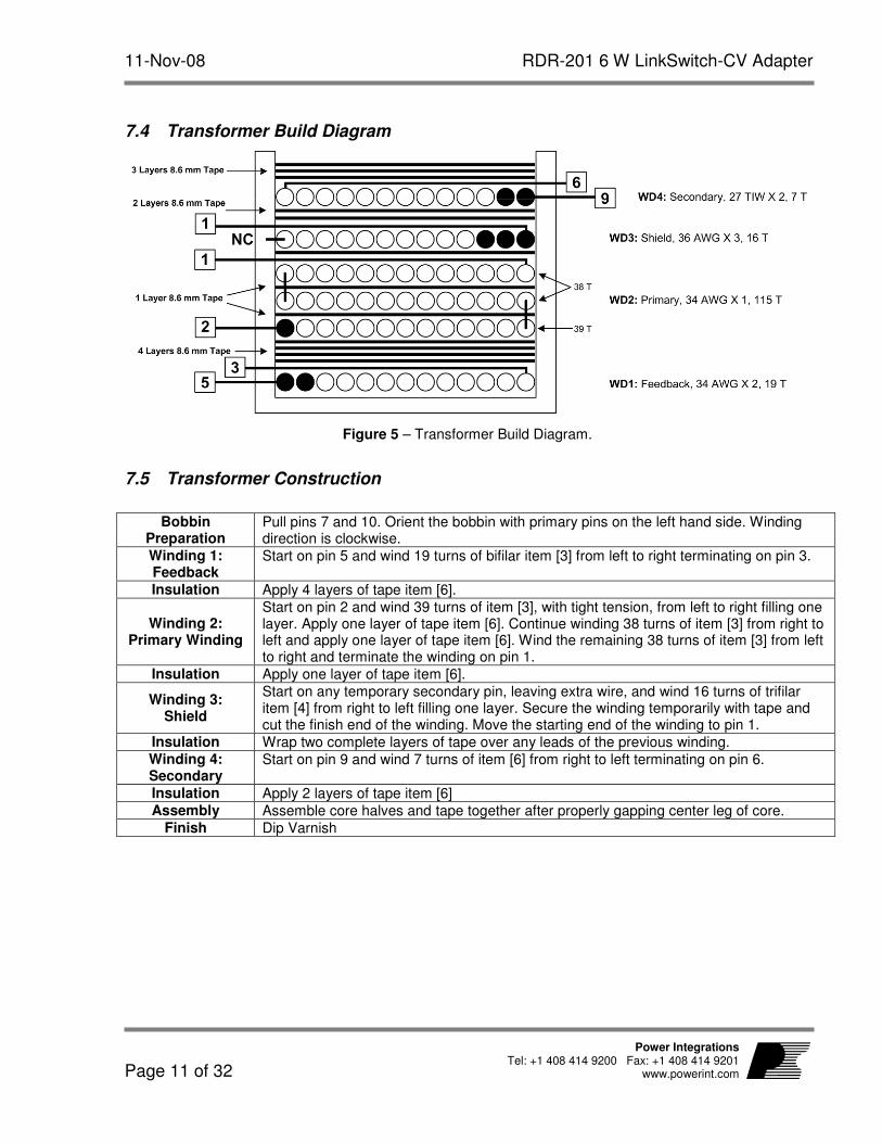
7.4 Transformer Build Diagram
Figure 5 – Transformer Build Diagram.
7.5 Transformer Construction
Bobbin
Preparation Pull pins 7 and 10. Orient the bobbin with primary pins on the left hand side. Winding direction is clockwise.
Winding 1: Feedback
Start on pin 5 and wind 19 turns of bifilar item [3] from left to right terminating on pin 3.
Insulation Apply 4 layers of tape item [6].
Winding 2: Primary Winding
Start on pin 2 and wind 39 turns of item [3], with tight tension, from left to right filling one layer. Apply one layer of tape item [6]. Continue winding 38 turns of item [3] from right to left and apply one layer of tape item [6]. Wind the remaining 38 turns of item [3] from left to right and terminate the winding on pin 1.
Insulation Apply one layer of tape item [6].
Winding 3: Shield
Start on any temporary secondary pin, leaving extra wire, and wind 16 turns of trifilar item [4] from right to left filling one layer. Secure the winding temporarily with tape and cut the finish end of the winding. Move the starting end of the winding to pin 1.
Insulation Wrap two complete layers of tape over any leads of the previous winding. Winding 4: Secondary
Start on pin 9 and wind 7 turns of item [6] from right to left terminating on pin 6.
Insulation Apply 2 layers of tape item [6] Assembly Assemble core halves and tape together after properly gapping center leg of core.
Finish Dip Varnish
RDR-201 6 W LinkSwitch-CV Adapter 11-Nov-08
Page 12 of 32
Power Integrations Tel: +1 408 414 9200 Fax: +1 408 414 9201 www.powerint.com
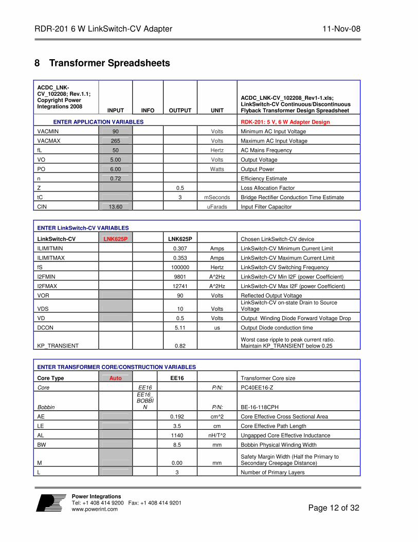
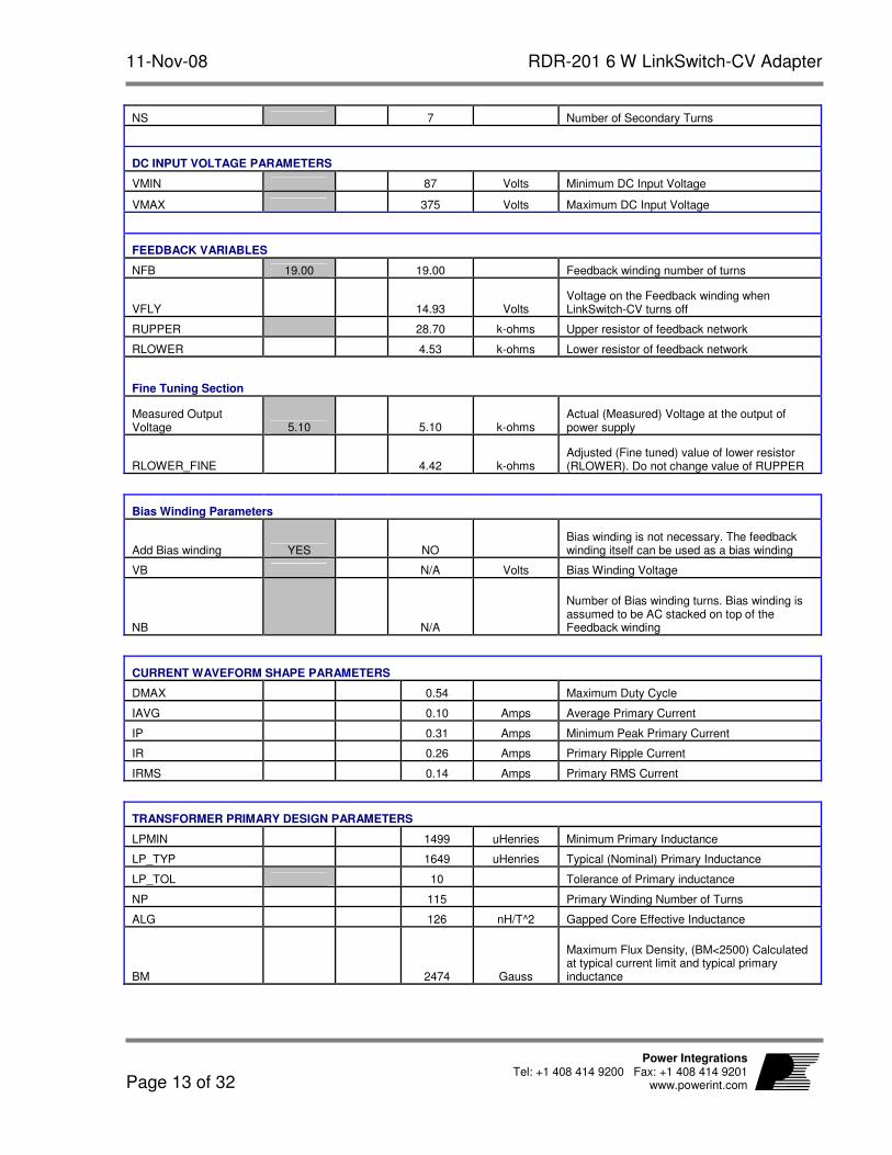
8 Transformer Spreadsheets
ACDC_LNK-CV_102208; Rev.1.1; Copyright Power Integrations 2008
INPUT INFO OUTPUT UNIT
ACDC_LNK-CV_102208_Rev1-1.xls; LinkSwitch-CV Continuous/Discontinuous Flyback Transformer Design Spreadsheet
ENTER APPLICATION VARIABLES RDK-201: 5 V, 6 W Adapter Design
VACMIN 90 Volts Minimum AC Input Voltage
VACMAX 265 Volts Maximum AC Input Voltage
fL 50 Hertz AC Mains Frequency
VO 5.00 Volts Output Voltage
PO 6.00 Watts Output Power
n 0.72 Efficiency Estimate
Z 0.5 Loss Allocation Factor
tC 3 mSeconds Bridge Rectifier Conduction Time Estimate
CIN 13.60 uFarads Input Filter Capacitor
ENTER LinkSwitch-CV VARIABLES
LinkSwitch-CV LNK625P LNK625P Chosen LinkSwitch-CV device
ILIMITMIN 0.307 Amps LinkSwitch-CV Minimum Current Limit
ILIMITMAX 0.353 Amps LinkSwitch-CV Maximum Current Limit
fS 100000 Hertz LinkSwitch-CV Switching Frequency
I2FMIN 9801 A^2Hz LinkSwitch-CV Min I2F (power Coefficient)
I2FMAX 12741 A^2Hz LinkSwitch-CV Max I2F (power Coefficient)
VOR 90 Volts Reflected Output Voltage
VDS 10 Volts LinkSwitch-CV on-state Drain to Source Voltage
VD 0.5 Volts Output Winding Diode Forward Voltage Drop
DCON 5.11 us Output Diode conduction time
KP_TRANSIENT 0.82 Worst case ripple to peak current ratio. Maintain KP_TRANSIENT below 0.25
ENTER TRANSFORMER CORE/CONSTRUCTION VARIABLES
Core Type Auto EE16 Transformer Core size
Core EE16 P/N: PC40EE16-Z
Bobbin
EE16_BOBBI
N P/N: BE-16-118CPH
AE 0.192 cm^2 Core Effective Cross Sectional Area
LE 3.5 cm Core Effective Path Length
AL 1140 nH/T^2 Ungapped Core Effective Inductance
BW 8.5 mm Bobbin Physical Winding Width
M 0.00 mm Safety Margin Width (Half the Primary to Secondary Creepage Distance)
L 3 Number of Primary Layers
11-Nov-08 RDR-201 6 W LinkSwitch-CV Adapter
Page 13 of 32
Power Integrations Tel: +1 408 414 9200 Fax: +1 408 414 9201
www.powerint.com
NS 7 Number of Secondary Turns
DC INPUT VOLTAGE PARAMETERS
VMIN 87 Volts Minimum DC Input Voltage
VMAX 375 Volts Maximum DC Input Voltage
FEEDBACK VARIABLES
NFB 19.00 19.00 Feedback winding number of turns
VFLY 14.93 Volts Voltage on the Feedback winding when LinkSwitch-CV turns off
RUPPER 28.70 k-ohms Upper resistor of feedback network
RLOWER 4.53 k-ohms Lower resistor of feedback network
Fine Tuning Section
Measured Output Voltage 5.10 5.10 k-ohms
Actual (Measured) Voltage at the output of power supply
RLOWER_FINE 4.42 k-ohms Adjusted (Fine tuned) value of lower resistor (RLOWER). Do not change value of RUPPER
Bias Winding Parameters
Add Bias winding YES NO Bias winding is not necessary. The feedback winding itself can be used as a bias winding
VB N/A Volts Bias Winding Voltage
NB N/A
Number of Bias winding turns. Bias winding is assumed to be AC stacked on top of the Feedback winding
CURRENT WAVEFORM SHAPE PARAMETERS
DMAX 0.54 Maximum Duty Cycle
IAVG 0.10 Amps Average Primary Current
IP 0.31 Amps Minimum Peak Primary Current
IR 0.26 Amps Primary Ripple Current
IRMS 0.14 Amps Primary RMS Current
TRANSFORMER PRIMARY DESIGN PARAMETERS
LPMIN 1499 uHenries Minimum Primary Inductance
LP_TYP 1649 uHenries Typical (Nominal) Primary Inductance
LP_TOL 10 Tolerance of Primary inductance
NP 115 Primary Winding Number of Turns
ALG 126 nH/T^2 Gapped Core Effective Inductance
BM 2474 Gauss
Maximum Flux Density, (BM<2500) Calculated at typical current limit and typical primary inductance
RDR-201 6 W LinkSwitch-CV Adapter 11-Nov-08
Page 14 of 32
Power Integrations Tel: +1 408 414 9200 Fax: +1 408 414 9201 www.powerint.com
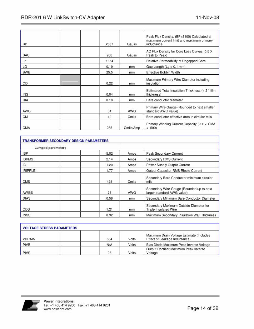
BP 2887 Gauss
Peak Flux Density, (BP<3100) Calculated at maximum current limit and maximum primary inductance
BAC 908 Gauss AC Flux Density for Core Loss Curves (0.5 X Peak to Peak)
ur 1654 Relative Permeability of Ungapped Core
LG 0.19 mm Gap Length (Lg > 0.1 mm)
BWE 25.5 mm Effective Bobbin Width
OD 0.22 mm Maximum Primary Wire Diameter including insulation
INS 0.04 mm Estimated Total Insulation Thickness (= 2 * film thickness)
DIA 0.18 mm Bare conductor diameter
AWG 34 AWG Primary Wire Gauge (Rounded to next smaller standard AWG value)
CM 40 Cmils Bare conductor effective area in circular mils
CMA 285 Cmils/Amp Primary Winding Current Capacity (200 < CMA < 500)
TRANSFORMER SECONDARY DESIGN PARAMETERS
Lumped parameters
ISP 5.02 Amps Peak Secondary Current
ISRMS 2.14 Amps Secondary RMS Current
IO 1.20 Amps Power Supply Output Current
IRIPPLE 1.77 Amps Output Capacitor RMS Ripple Current
CMS 428 Cmils Secondary Bare Conductor minimum circular mils
AWGS 23 AWG Secondary Wire Gauge (Rounded up to next larger standard AWG value)
DIAS 0.58 mm Secondary Minimum Bare Conductor Diameter
ODS 1.21 mm Secondary Maximum Outside Diameter for Triple Insulated Wire
INSS 0.32 mm Maximum Secondary Insulation Wall Thickness
VOLTAGE STRESS PARAMETERS
VDRAIN 584 Volts Maximum Drain Voltage Estimate (Includes Effect of Leakage Inductance)
PIVB N/A Volts Bias Diode Maximum Peak Inverse Voltage
PIVS 28 Volts Output Rectifier Maximum Peak Inverse Voltage
11-Nov-08 RDR-201 6 W LinkSwitch-CV Adapter
Page 15 of 32
Power Integrations Tel: +1 408 414 9200 Fax: +1 408 414 9201
www.powerint.com
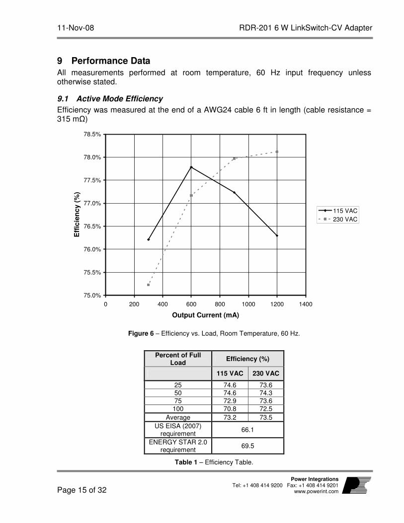
9 Performance Data
All measurements performed at room temperature, 60 Hz input frequency unless otherwise stated.
9.1 Active Mode Efficiency
Efficiency was measured at the end of a AWG24 cable 6 ft in length (cable resistance = 315 mΩ)
75.0%
75.5%
76.0%
76.5%
77.0%
77.5%
78.0%
78.5%
0 200 400 600 800 1000 1200 1400
Output Current (mA)
Eff
icie
ncy (
%)
115 VAC
230 VAC
Figure 6 – Efficiency vs. Load, Room Temperature, 60 Hz.
Percent of Full
Load Efficiency (%)
115 VAC 230 VAC
25 74.6 73.6 50 74.6 74.3
75 72.9 73.6
100 70.8 72.5
Average 73.2 73.5
US EISA (2007) requirement
66.1
ENERGY STAR 2.0 requirement
69.5
Table 1 – Efficiency Table.

RDR-201 6 W LinkSwitch-CV Adapter 11-Nov-08
Page 16 of 32
Power Integrations Tel: +1 408 414 9200 Fax: +1 408 414 9201 www.powerint.com
9.2 Energy Efficiency Requirements
The external power supply requirements below all require meeting active mode efficiency and no-load input power limits. Minimum active mode efficiency is defined as the average efficiency of 25, 50, 75 and 100% of output current (based on the nameplate output current rating). For adapters that are single input voltage only then the measurement is made at the rated single nominal input voltage (115 VAC or 230 VAC), for universal input adapters the measurement is made at both nominal input voltages (115 VAC and 230 VAC). To meet the standard the measured average efficiency (or efficiencies for universal input supplies) must be greater than or equal to the efficiency specified by the standard. The test method can be found here: http://www.energystar.gov/ia/partners/prod_development/downloads/power_supplies/EPSupplyEffic_TestMethod_0804.pdf For the latest up to date information please visit the PI Green Room: http://www.powerint.com/greenroom/regulations.htm
11-Nov-08 RDR-201 6 W LinkSwitch-CV Adapter
Page 17 of 32
Power Integrations Tel: +1 408 414 9200 Fax: +1 408 414 9201
www.powerint.com
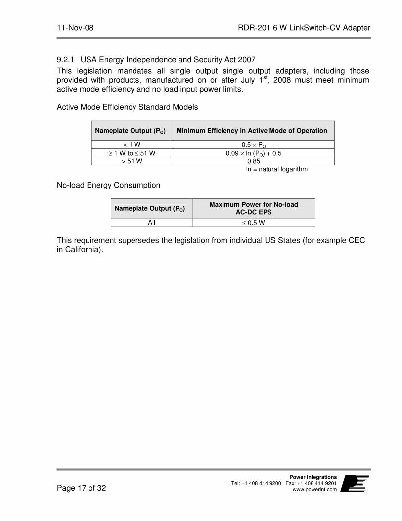
9.2.1 USA Energy Independence and Security Act 2007
This legislation mandates all single output single output adapters, including those provided with products, manufactured on or after July 1st, 2008 must meet minimum active mode efficiency and no load input power limits. Active Mode Efficiency Standard Models
Nameplate Output (PO) Minimum Efficiency in Active Mode of Operation
< 1 W 0.5 × PO
≥ 1 W to ≤ 51 W 0.09 × ln (PO) + 0.5 > 51 W 0.85
ln = natural logarithm
No-load Energy Consumption
Nameplate Output (PO) Maximum Power for No-load
AC-DC EPS
All ≤ 0.5 W
This requirement supersedes the legislation from individual US States (for example CEC in California).
RDR-201 6 W LinkSwitch-CV Adapter 11-Nov-08
Page 18 of 32
Power Integrations Tel: +1 408 414 9200 Fax: +1 408 414 9201 www.powerint.com
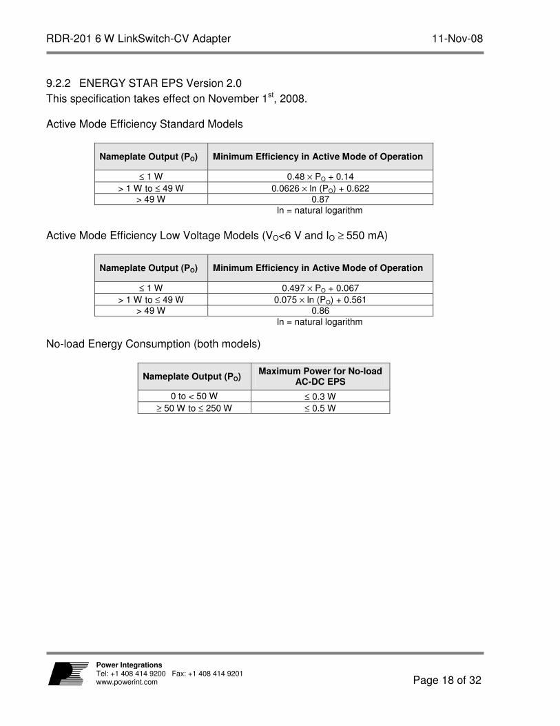
9.2.2 ENERGY STAR EPS Version 2.0
This specification takes effect on November 1st, 2008. Active Mode Efficiency Standard Models
Nameplate Output (PO) Minimum Efficiency in Active Mode of Operation
≤ 1 W 0.48 × PO + 0.14
> 1 W to ≤ 49 W 0.0626 × ln (PO) + 0.622 > 49 W 0.87
ln = natural logarithm
Active Mode Efficiency Low Voltage Models (VO<6 V and IO ≥ 550 mA)
Nameplate Output (PO) Minimum Efficiency in Active Mode of Operation
≤ 1 W 0.497 × PO + 0.067
> 1 W to ≤ 49 W 0.075 × ln (PO) + 0.561 > 49 W 0.86
ln = natural logarithm
No-load Energy Consumption (both models)
Nameplate Output (PO) Maximum Power for No-load
AC-DC EPS
0 to < 50 W ≤ 0.3 W
≥ 50 W to ≤ 250 W ≤ 0.5 W
11-Nov-08 RDR-201 6 W LinkSwitch-CV Adapter
Page 19 of 32
Power Integrations Tel: +1 408 414 9200 Fax: +1 408 414 9201
www.powerint.com
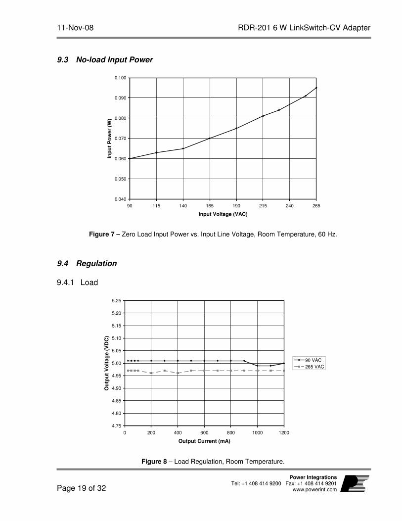
9.3 No-load Input Power
0.040
0.050
0.060
0.070
0.080
0.090
0.100
90 115 140 165 190 215 240 265
Input Voltage (VAC)
Inp
ut
Po
we
r (W
)
Figure 7 – Zero Load Input Power vs. Input Line Voltage, Room Temperature, 60 Hz.
9.4 Regulation
9.4.1 Load
4.75
4.80
4.85
4.90
4.95
5.00
5.05
5.10
5.15
5.20
5.25
0 200 400 600 800 1000 1200
Output Current (mA)
Ou
tpu
t V
olt
ag
e (
VD
C)
90 VAC
265 VAC
Figure 8 – Load Regulation, Room Temperature.
RDR-201 6 W LinkSwitch-CV Adapter 11-Nov-08
Page 20 of 32
Power Integrations Tel: +1 408 414 9200 Fax: +1 408 414 9201 www.powerint.com
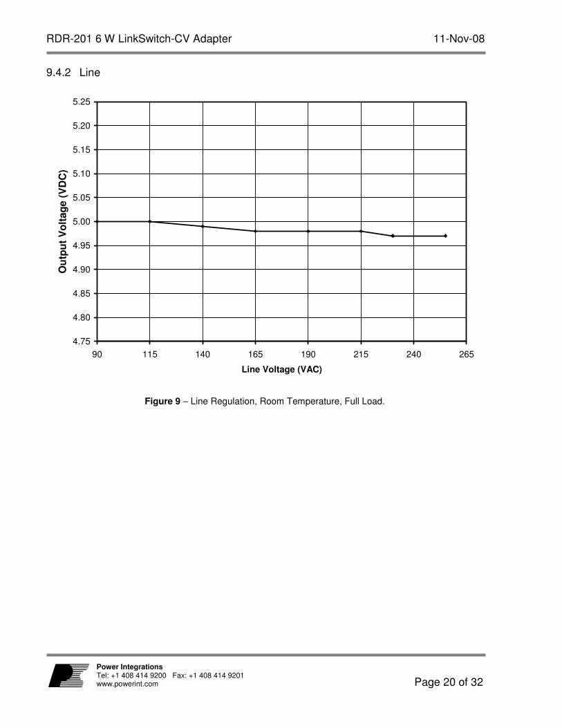
9.4.2 Line
4.75
4.80
4.85
4.90
4.95
5.00
5.05
5.10
5.15
5.20
5.25
90 115 140 165 190 215 240 265
Line Voltage (VAC)
Ou
tpu
t V
olt
ag
e (
VD
C)
Figure 9 – Line Regulation, Room Temperature, Full Load.
11-Nov-08 RDR-201 6 W LinkSwitch-CV Adapter
Page 21 of 32
Power Integrations Tel: +1 408 414 9200 Fax: +1 408 414 9201
www.powerint.com
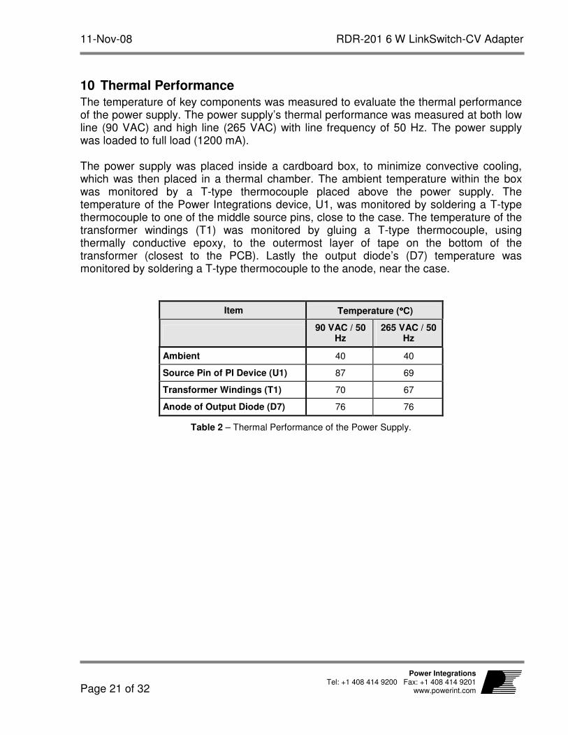
10 Thermal Performance
The temperature of key components was measured to evaluate the thermal performance of the power supply. The power supply’s thermal performance was measured at both low line (90 VAC) and high line (265 VAC) with line frequency of 50 Hz. The power supply was loaded to full load (1200 mA). The power supply was placed inside a cardboard box, to minimize convective cooling, which was then placed in a thermal chamber. The ambient temperature within the box was monitored by a T-type thermocouple placed above the power supply. The temperature of the Power Integrations device, U1, was monitored by soldering a T-type thermocouple to one of the middle source pins, close to the case. The temperature of the transformer windings (T1) was monitored by gluing a T-type thermocouple, using thermally conductive epoxy, to the outermost layer of tape on the bottom of the transformer (closest to the PCB). Lastly the output diode’s (D7) temperature was monitored by soldering a T-type thermocouple to the anode, near the case.
Item Temperature (°°°°C)
90 VAC / 50
Hz 265 VAC / 50
Hz
Ambient 40 40
Source Pin of PI Device (U1) 87 69
Transformer Windings (T1) 70 67
Anode of Output Diode (D7) 76 76
Table 2 – Thermal Performance of the Power Supply.
RDR-201 6 W LinkSwitch-CV Adapter 11-Nov-08
Page 22 of 32
Power Integrations Tel: +1 408 414 9200 Fax: +1 408 414 9201 www.powerint.com
11 Waveforms
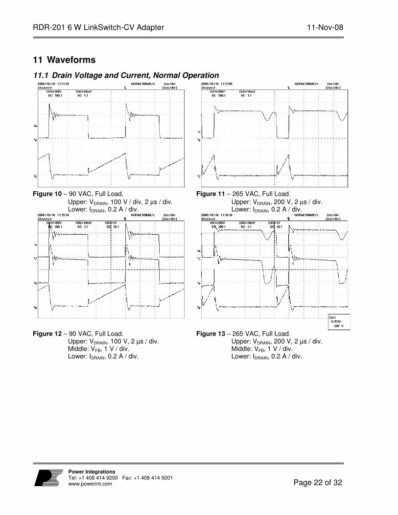
11.1 Drain Voltage and Current, Normal Operation
Figure 10 – 90 VAC, Full Load.
Upper: VDRAIN, 100 V / div, 2 µs / div. Lower: IDRAIN, 0.2 A / div.
Figure 11 – 265 VAC, Full Load.
Upper: VDRAIN, 200 V, 2 µs / div. Lower: IDRAIN, 0.2 A / div.
Figure 12 – 90 VAC, Full Load.
Upper: VDRAIN, 100 V, 2 µs / div. Middle: VFB, 1 V / div. Lower: IDRAIN, 0.2 A / div.
Figure 13 – 265 VAC, Full Load. Upper: VDRAIN, 200 V, 2 µs / div. Middle: VFB, 1 V / div. Lower: IDRAIN, 0.2 A / div.
11-Nov-08 RDR-201 6 W LinkSwitch-CV Adapter
Page 23 of 32
Power Integrations Tel: +1 408 414 9200 Fax: +1 408 414 9201
www.powerint.com
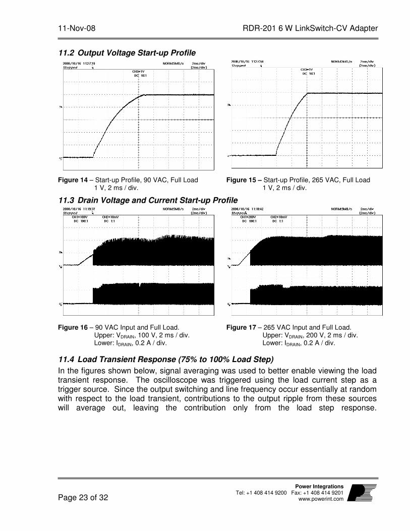
11.2 Output Voltage Start-up Profile
Figure 14 – Start-up Profile, 90 VAC, Full Load 1 V, 2 ms / div.
Figure 15 – Start-up Profile, 265 VAC, Full Load 1 V, 2 ms / div.
11.3 Drain Voltage and Current Start-up Profile
Figure 16 – 90 VAC Input and Full Load. Upper: VDRAIN, 100 V, 2 ms / div. Lower: IDRAIN, 0.2 A / div.
Figure 17 – 265 VAC Input and Full Load. Upper: VDRAIN, 200 V, 2 ms / div. Lower: IDRAIN, 0.2 A / div.
11.4 Load Transient Response (75% to 100% Load Step)
In the figures shown below, signal averaging was used to better enable viewing the load transient response. The oscilloscope was triggered using the load current step as a trigger source. Since the output switching and line frequency occur essentially at random with respect to the load transient, contributions to the output ripple from these sources will average out, leaving the contribution only from the load step response.
RDR-201 6 W LinkSwitch-CV Adapter 11-Nov-08
Page 24 of 32
Power Integrations Tel: +1 408 414 9200 Fax: +1 408 414 9201 www.powerint.com
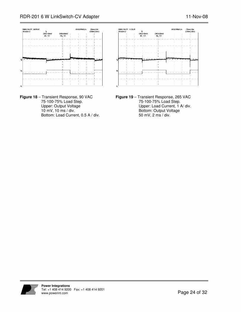
Figure 18 – Transient Response, 90 VAC 75-100-75% Load Step. Upper: Output Voltage 10 mV, 10 ms / div. Bottom: Load Current, 0.5 A / div.
Figure 19 – Transient Response, 265 VAC 75-100-75% Load Step. Upper: Load Current, 1 A/ div. Bottom: Output Voltage 50 mV, 2 ms / div.

11-Nov-08 RDR-201 6 W LinkSwitch-CV Adapter
Page 25 of 32
Power Integrations Tel: +1 408 414 9200 Fax: +1 408 414 9201
www.powerint.com
11.5 Output Ripple Measurements
11.5.1 Ripple Measurement Technique
For DC output ripple measurements, use a modified oscilloscope test probe to reduce spurious signals. Details of the probe modification are provided in figures below. Tie two capacitors in parallel across the probe tip of the 4987BA probe adapter. Use a
0.1 µF/50 V ceramic capacitor and a 1.0 µF/50 V aluminum-electrolytic capacitor. The aluminum-electrolytic capacitor is polarized, so always maintain proper polarity across DC outputs.
Figure 20 – Oscilloscope Probe Prepared for Ripple Measurement. (End Cap and Ground Lead Removed)
Figure 21 – Oscilloscope Probe with Probe Master (www.probemaster.com) 4987A BNC Adapter. (Modified with wires for ripple measurement, and two parallel decoupling capacitors added)
Probe Ground
Probe Tip
RDR-201 6 W LinkSwitch-CV Adapter 11-Nov-08
Page 26 of 32
Power Integrations Tel: +1 408 414 9200 Fax: +1 408 414 9201 www.powerint.com
11.5.2 Measurement Results
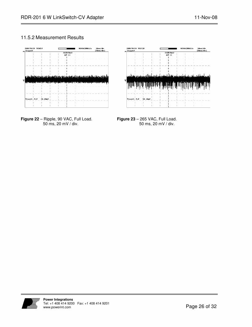
Figure 22 – Ripple, 90 VAC, Full Load. 50 ms, 20 mV / div.
Figure 23 – 265 VAC, Full Load. 50 ms, 20 mV / div.
11-Nov-08 RDR-201 6 W LinkSwitch-CV Adapter
Page 27 of 32
Power Integrations Tel: +1 408 414 9200 Fax: +1 408 414 9201
www.powerint.com
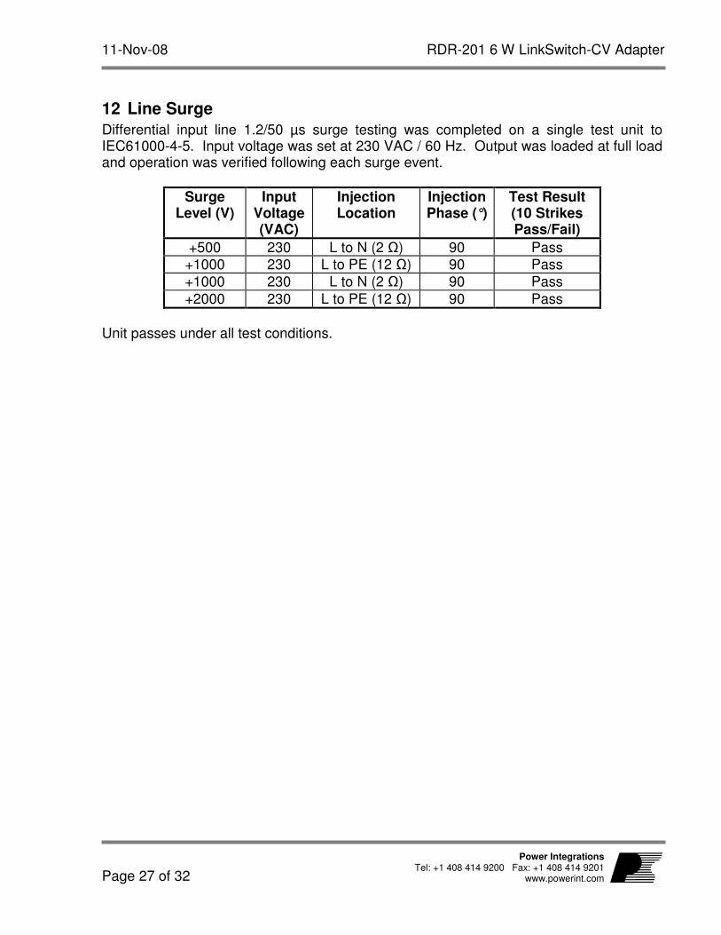
12 Line Surge
Differential input line 1.2/50 µs surge testing was completed on a single test unit to IEC61000-4-5. Input voltage was set at 230 VAC / 60 Hz. Output was loaded at full load and operation was verified following each surge event.
Surge Level (V)
Input Voltage (VAC)
Injection Location
Injection Phase (°)
Test Result (10 Strikes Pass/Fail)
+500 230 L to N (2 Ω) 90 Pass +1000 230 L to PE (12 Ω) 90 Pass
+1000 230 L to N (2 Ω) 90 Pass
+2000 230 L to PE (12 Ω) 90 Pass
Unit passes under all test conditions.
RDR-201 6 W LinkSwitch-CV Adapter 11-Nov-08
Page 28 of 32
Power Integrations Tel: +1 408 414 9200 Fax: +1 408 414 9201 www.powerint.com
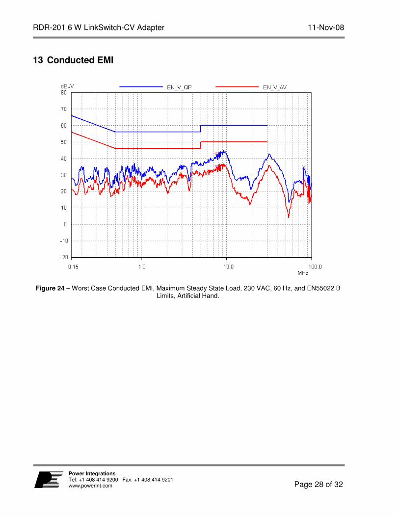
13 Conducted EMI
Figure 24 – Worst Case Conducted EMI, Maximum Steady State Load, 230 VAC, 60 Hz, and EN55022 B Limits, Artificial Hand.
11-Nov-08 RDR-201 6 W LinkSwitch-CV Adapter
Page 29 of 32
Power Integrations Tel: +1 408 414 9200 Fax: +1 408 414 9201
www.powerint.com
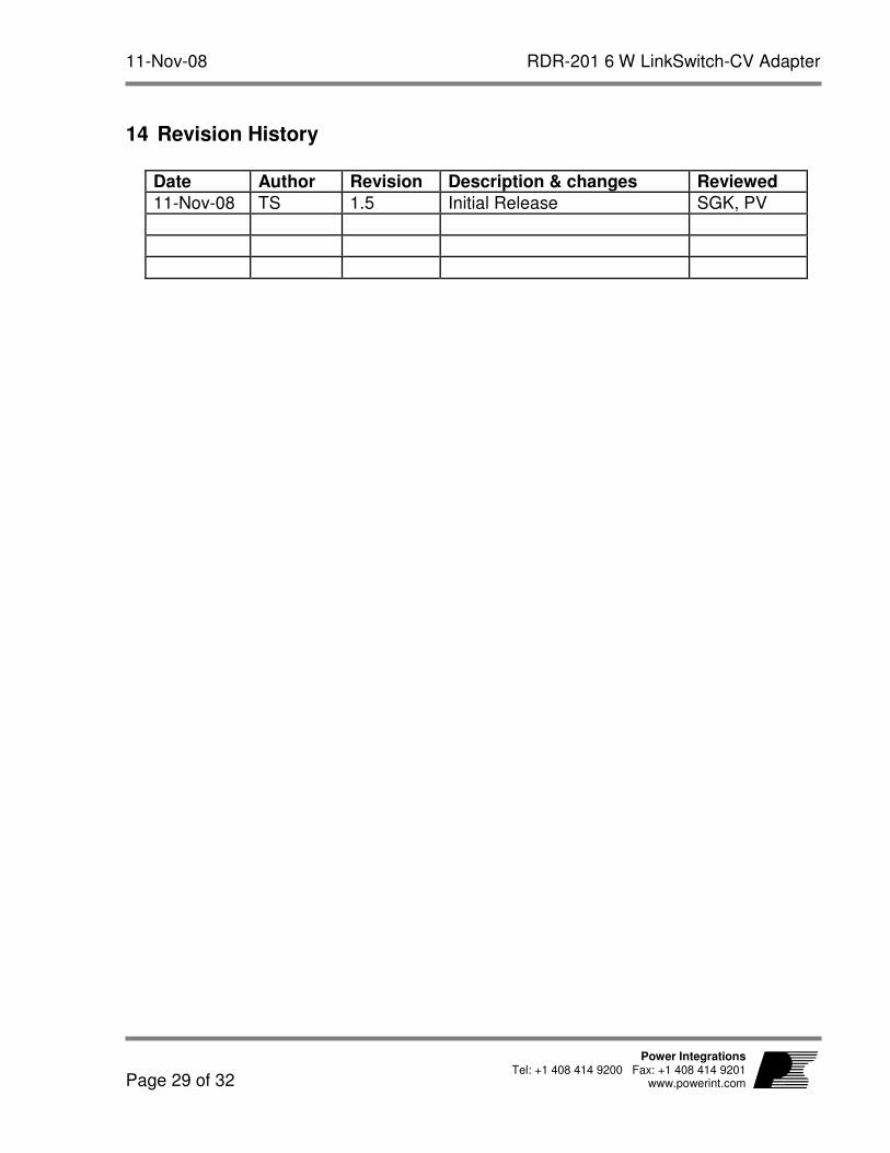
14 Revision History
Date Author Revision Description & changes Reviewed
11-Nov-08 TS 1.5 Initial Release SGK, PV

RDR-201 6 W LinkSwitch-CV Adapter 11-Nov-08
Page 30 of 32
Power Integrations Tel: +1 408 414 9200 Fax: +1 408 414 9201 www.powerint.com
Notes

11-Nov-08 RDR-201 6 W LinkSwitch-CV Adapter
Page 31 of 32
Power Integrations Tel: +1 408 414 9200 Fax: +1 408 414 9201
www.powerint.com
Notes

RDR-201 6 W LinkSwitch-CV Adapter 11-Nov-08
Page 32 of 32
Power Integrations Tel: +1 408 414 9200 Fax: +1 408 414 9201 www.powerint.com
For the latest updates, visit our website: www.powerint.com
Power Integrations reserves the right to make changes to its products at any time to improve reliability or
manufacturability. Power Integrations does not assume any liability arising from the use of any device or circuit
described herein. POWER INTEGRATIONS MAKES NO WARRANTY HEREIN AND SPECIFICALLY DISCLAIMS ALL
WARRANTIES INCLUDING, WITHOUT LIMITATION, THE IMPLIED WARRANTIES OF MERCHANTABILITY,
FITNESS FOR A PARTICULAR PURPOSE, AND NON-INFRINGEMENT OF THIRD PARTY RIGHTS.
PATENT INFORMATION
The products and applications illustrated herein (including transformer construction and circuits external to the products)
may be covered by one or more U.S. and foreign patents, or potentially by pending U.S. and foreign patent applications
assigned to Power Integrations. A complete list of Power Integrations’ patents may be found at www.powerint.com.
Power Integrations grants its customers a license under certain patent rights as set forth at
http://www.powerint.com/ip.htm.
The PI Logo, TOPSwitch, TinySwitch, LinkSwitch, DPA-Switch, PeakSwitch, EcoSmart, Clampless, E-Shield, Filterfuse, StackFET,
PI Expert and PI FACTS are trademarks of Power Integrations, Inc. Other trademarks are property of their respective
companies. ©Copyright 2008 Power Integrations, Inc.
Power Integrations Worldwide Sales Support Locations
WORLD HEADQUARTERS 5245 Hellyer Avenue San Jose, CA 95138, USA. Main: +1-408-414-9200 Customer Service: Phone: +1-408-414-9665 Fax: +1-408-414-9765 e-mail: [email protected]
GERMANY Rueckertstrasse 3 D-80336, Munich Germany Phone: +49-89-5527-3911 Fax: +49-89-5527-3920 e-mail: [email protected]
JAPAN Kosei Dai-3 Bldg., 2-12-11, Shin-Yokohama, Kohoku-ku, Yokohama-shi, Kanagawa 222-0033 Phone: +81-45-471-1021 Fax: +81-45-471-3717 e-mail: [email protected]
TAIWAN 5F, No. 318, Nei Hu Rd., Sec. 1 Nei Hu Dist. Taipei, Taiwan 114, R.O.C. Phone: +886-2-2659-4570 Fax: +886-2-2659-4550 e-mail: [email protected]
CHINA (SHANGHAI) Rm 1601/1610, Tower 1, Kerry Everbright City No. 218 Tianmu Road West, Shanghai, P.R.C. 200070 Phone: +86-21-6354-6323 Fax: +86-21-6354-6325 e-mail: [email protected]
INDIA #1, 14
th Main Road
Vasanthanagar Bangalore-560052 India Phone: +91-80-41138020 Fax: +91-80-41138023 e-mail: [email protected]
KOREA RM 602, 6FL Korea City Air Terminal B/D, 159-6 Samsung-Dong, Kangnam-Gu, Seoul, 135-728, Korea Phone: +82-2-2016-6610 Fax: +82-2-2016-6630 e-mail: [email protected]
UNITED KINGDOM 1st Floor, St. James’s House East Street, Farnham Surrey, GU9 7TJ United Kingdom Phone: +44 (0) 1252-730-141 Fax: +44 (0) 1252-727-689 e-mail: [email protected]
CHINA (SHENZHEN) Rm A, B & C 4
th Floor, Block C,
Electronics Science and Technology Building, 2070 Shennan Zhong Rd, Shenzhen, Guangdong, China, 518031 Phone: +86-755-8379-3243 Fax: +86-755-8379-5828 e-mail: [email protected]
ITALY Via De Amicis 2 20091 Bresso MI – Italy Phone: +39-028-928-6000 Fax: +39-028-928-6009 e-mail: [email protected]
SINGAPORE 51 Newton Road, #15-08/10 Goldhill Plaza, Singapore, 308900 Phone: +65-6358-2160 Fax: +65-6358-2015 e-mail: [email protected]
APPLICATIONS HOTLINE World Wide +1-408-414-9660 APPLICATIONS FAX World Wide +1-408-414-9760
Recommended