9. ELECTRONIC DEVICES
GIST
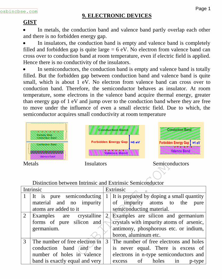
In metals, the conduction band and valence band partly overlap each other
and there is no forbidden energy gap.
In insulators, the conduction band is empty and valence band is completely
filled and forbidden gap is quite large = 6 eV. No electron from valence band can
cross over to conduction band at room temperature, even if electric field is applied.
Hence there is no conductivity of the insulators.
In semiconductors, the conduction band is empty and valence band is totally
filled. But the forbidden gap between conduction band and valence band is quite
small, which is about 1 eV. No electron from valence band can cross over to
conduction band. Therefore, the semiconductor behaves as insulator. At room
temperature, some electrons in the valence band acquire thermal energy, greater
than energy gap of 1 eV and jump over to the conduction band where they are free
to move under the influence of even a small electric field. Due to which, the
semiconductor acquires small conductivity at room temperature
Metals Insulators Semiconductors
Distinction between Intrinsic and Extrinsic Semiconductor
Intrinsic Extrinsic
1 It is pure semiconducting
material and no impurity
atoms are added to it
1 It is prepared by doping a small quantity
of impurity atoms to the pure
semiconducting material.
2 Examples are crystalline
forms of pure silicon and
germanium.
2 Examples are silicon and germanium
crystals with impurity atoms of arsenic,
antimony, phosphorous etc. or indium,
boron, aluminum etc.
3 The number of free electron in
conduction band and the
number of holes in valence
band is exactly equal and very
3 The number of free electrons and holes
is never equal. There is excess of
electrons in n-type semiconductors and
excess of holes in p-type
Downloaded from www.studiestoday.com
Downloaded from www.studiestoday.com
osbincbse.com
OSBINCBSE.COM
OSBINCBSE.COM
OSBINCBSE.COM
Page 1
small indeed. semiconductors.
4 Its electrical conductivity is
low
4 Its electrical conductivity is high.
5 Its electrical conductivity is a
function of temperature alone.
5 Its electrical conductivity depends upon
the temperature as well as on the
quantity of impurity atoms doped in the
structure.
Distinction between n-type and p-type semiconductors
n-type semiconductors p-type semiconductors
1 It is an extrinsic
semiconductors which is
obtained by doping the
impurity atoms of Vth group
of periodic table to the pure
germanium or silicon
semiconductor.
1 It is an intrinsic semiconductors which
is obtained by doping the impurity
atoms of III group of periodic table to
the pure germanium or silicon
semiconductor.
2 The impurity atoms added,
provide extra electrons in the
structure, and are called donor
atoms.
2 The impurity atoms added, create
vacancies of electrons (i.e. holes) in the
structure and are called acceptor atoms.
3 The electrons are majority
carriers and holes are minority
carriers.
3 The holes are majority carriers and
electrons are minority carriers.
4 The electron density (ne) is
much greater than the hole
density (nh)i.e. ne>>(nh)
4 The hole density (ne) is much greater
than the electron density (nh)i.e. nh>> ne
5 The donor energy level is
close to the conduction band
and far away from valence
band.
5 The acceptor energy level is close to
valence band and is far away from the
conduction band.
6 The Fermi energy level lies in
between the donor energy
level and conduction band.
6 The Fermi energy level lies in between
the acceptor energy level and valence
band.
P-n junction diode
Two important processes occur during the formation of p-n junction diffusion and
drift. The motion of majority charge carriers give rise to diffusion current.
Due to the space charge on n-side junction and negative space charge region on p-
side the electric field is set up and potential barrier develops at the junction Due to
Downloaded from www.studiestoday.com
Downloaded from www.studiestoday.com
osbincbse.com
OSBINCBSE.COM
OSBINCBSE.COM
OSBINCBSE.COM
Page 2
electric field e- on p-side moves to n and holes from n-side to p-side which is
called drift current.
In equilibrium state, there is no current across p-n junction and potential barrier
across p-n junction has maximum value.
The width of the depletion region and magnitude of barrier potential depends on
the nature of semiconductor and doping concentration on two sides of p-n junction.
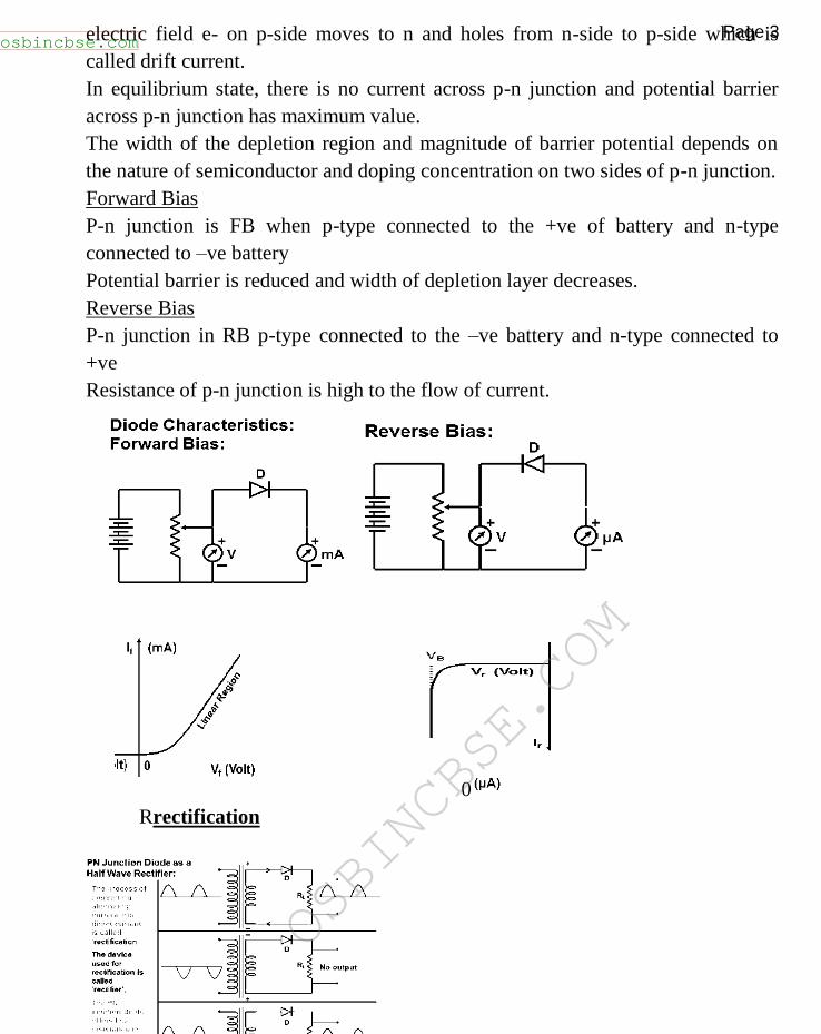
Forward Bias
P-n junction is FB when p-type connected to the +ve of battery and n-type
connected to –ve battery
Potential barrier is reduced and width of depletion layer decreases.
Reverse Bias
P-n junction in RB p-type connected to the –ve battery and n-type connected to
+ve
Resistance of p-n junction is high to the flow of current.
0
Rrectification
Downloaded from www.studiestoday.com
Downloaded from www.studiestoday.com
osbincbse.com
OSBINCBSE.COM
OSBINCBSE.COM
OSBINCBSE.COM
Page 3
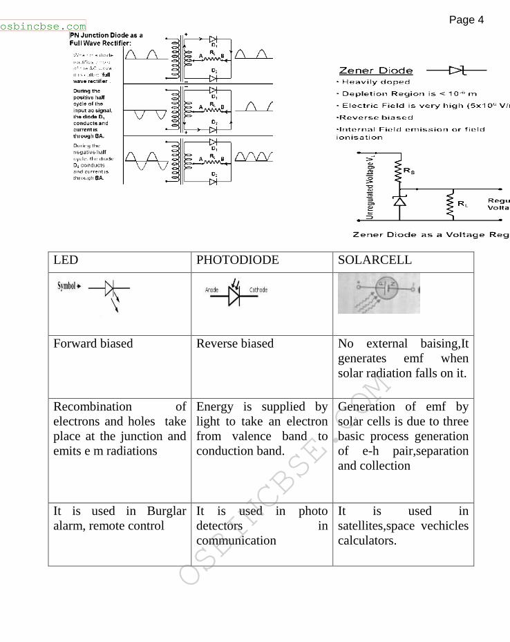
LED PHOTODIODE SOLARCELL
Forward biased Reverse biased No external baising,It
generates emf when
solar radiation falls on it.
Recombination of
electrons and holes take
place at the junction and
emits e m radiations
Energy is supplied by
light to take an electron
from valence band to
conduction band.
Generation of emf by
solar cells is due to three
basic process generation
of e-h pair,separation
and collection
It is used in Burglar
alarm, remote control
It is used in photo
detectors in
communication
It is used in
satellites,space vechicles
calculators.
Downloaded from www.studiestoday.com
Downloaded from www.studiestoday.com
osbincbse.com
OSBINCBSE.COM
OSBINCBSE.COM
OSBINCBSE.COM
Page 4
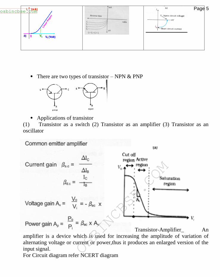
• There are two types of transistor – NPN & PNP
• Applications of transistor
(1) Transistor as a switch (2) Transistor as an amplifier (3) Transistor as an
oscillator
Transistor-Amplifier_ An
amplifier is a device which is used for increasing the amplitude of variation of
alternating voltage or current or power,thus it produces an enlarged version of the
input signal.
For Circuit diagram refer NCERT diagram
Downloaded from www.studiestoday.com
Downloaded from www.studiestoday.com
osbincbse.com
OSBINCBSE.COM
OSBINCBSE.COM
OSBINCBSE.COM
Page 5
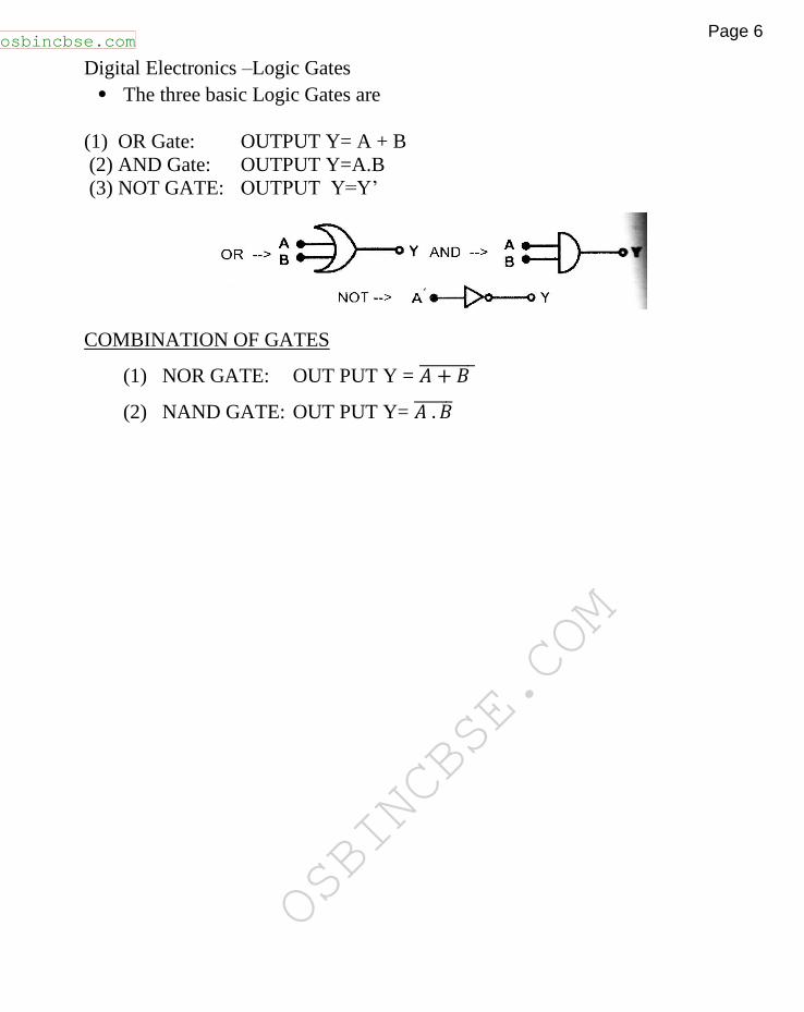
Digital Electronics –Logic Gates
• The three basic Logic Gates are
(1) OR Gate: OUTPUT Y= A + B
(2) AND Gate: OUTPUT Y=A.B
(3) NOT GATE: OUTPUT Y=Y’
COMBINATION OF GATES
(1) NOR GATE: OUT PUT Y = 𝐴 + 𝐵 ̅̅ ̅̅ ̅̅ ̅̅
(2) NAND GATE: OUT PUT Y= 𝐴 . 𝐵̅̅ ̅̅ ̅̅
Downloaded from www.studiestoday.com
Downloaded from www.studiestoday.com
osbincbse.com
OSBINCBSE.COM
OSBINCBSE.COM
OSBINCBSE.COM
Page 6
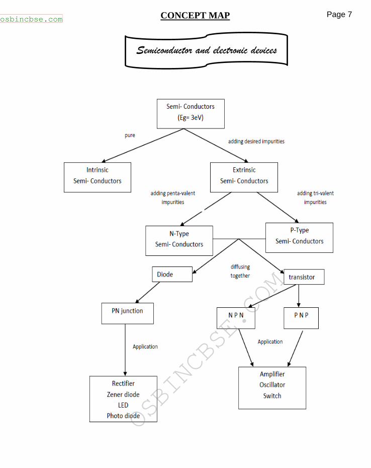
CONCEPT MAP
Semiconductor and electronic devices
Downloaded from www.studiestoday.com
Downloaded from www.studiestoday.com
osbincbse.com
OSBINCBSE.COM
OSBINCBSE.COM
OSBINCBSE.COM
Page 7
QUESTIONS
SEMICONDUCTORS
1. What is the order of energy gap in an intrinsic semiconductor? (1)
2. How does the energy gap vary in a semiconductor when doped with penta -
valent element? (1)
3. How does the conductivity change with temperature in semiconductor?(1)
4. What type of semiconductor we get when: Ge is doped with Indium? Si is doped
with Bismuth? (1)
5. In a semiconductor concentration of electron is 8 x 1013cm-3 and holes 5 x 10¹²
cm-2 : is it P or N type semiconductor? (1)
6. Draw energy gap diagram of a P Type semiconductor? (1)
7. What is Fermi energy level? (1)
8. Energy gap of a conductor, semiconductor, insulator are E1, E2, E3 respectively.
Arrange them in increasing order. (1)
9. Name the factor that determines the element as a conductor or semiconductor?
(1)
10. Why semiconductors are opaque to visible light but transparent to infrared
radiations? (2)
Ans: The photons of infrared radiation have smaller energies, so they fail to excite
the electrons in the valence band. Hence infrared radiations pass through the
semiconductors as such; i.e. a semiconductor is transparent to infrared radiation
11. The ratio of number of free electrons to holes ne/nh for two different materials
A and B are 1 and <1 respectively. Name the type of semiconductor to which A
and B belongs. (2)
Ans: If ne/nh =1 . Hence A is intrinsic semiconductor. If ne/nh<1 , ne<nh hence B is
P-type.
12. Differentiate the electrical conductivity of both types of extrinsic
semiconductors in terms of the energy band picture. (2)
P-N JUNCTION DIODE
1. How does the width of depletion layer change, in reverse bias of a p-n junction
diode? (1)
Downloaded from www.studiestoday.com
Downloaded from www.studiestoday.com
osbincbse.com
OSBINCBSE.COM
OSBINCBSE.COM
OSBINCBSE.COM
Page 8
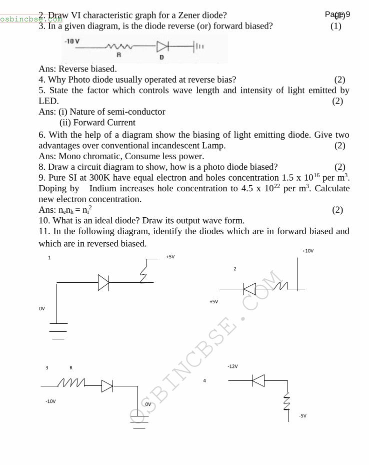
2. Draw VI characteristic graph for a Zener diode? (1)
3. In a given diagram, is the diode reverse (or) forward biased? (1)
Ans: Reverse biased.
4. Why Photo diode usually operated at reverse bias? (2)
5. State the factor which controls wave length and intensity of light emitted by
LED. (2)
Ans: (i) Nature of semi-conductor
(ii) Forward Current
6. With the help of a diagram show the biasing of light emitting diode. Give two
advantages over conventional incandescent Lamp. (2)
Ans: Mono chromatic, Consume less power.
8. Draw a circuit diagram to show, how is a photo diode biased? (2)
9. Pure SI at 300K have equal electron and holes concentration 1.5 x 10¹⁶ per m3.
Doping by Indium increases hole concentration to 4.5 x 10²² per m3. Calculate
new electron concentration.
Ans: nenh = ni2 (2)
10. What is an ideal diode? Draw its output wave form.
11. In the following diagram, identify the diodes which are in forward biased and
which are in reversed biased.
+10V
2
-10V
R
0V
3
-5V
-12V
4
1 +5V
0V
+5V
Downloaded from www.studiestoday.com
Downloaded from www.studiestoday.com
osbincbse.com
OSBINCBSE.COM
OSBINCBSE.COM
OSBINCBSE.COM
Page 9
12. A semiconductor has equal electron and hole concentrations of 6x10⁸/m3. On
doping with a certain impurity, the electron concentration increases to 9x10¹²/ m3.
(2)
(i) Identify the new semiconductor obtained after doping.
(ii) Calculate the new hole concentrations.
Ans: (i) n-type semiconductor.
(ii) nenh=ni 2 => nh=6x108 x6x108 = 4x10⁴ perm2
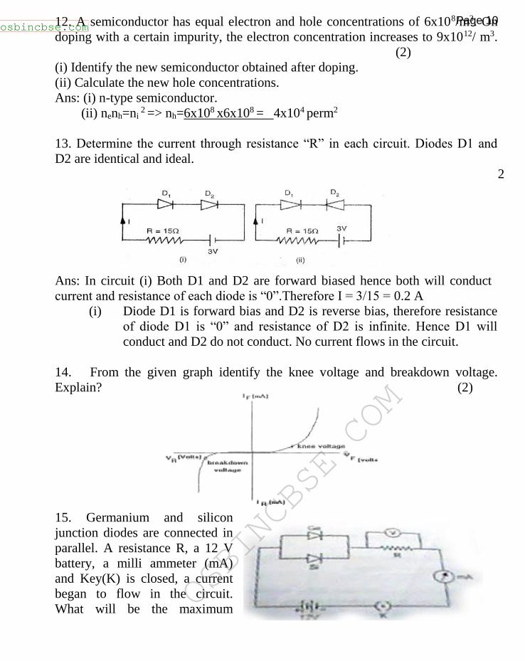
13. Determine the current through resistance “R” in each circuit. Diodes D1 and
D2 are identical and ideal.
2
Ans: In circuit (i) Both D1 and D2 are forward biased hence both will conduct
current and resistance of each diode is “0”.Therefore I = 3/15 = 0.2 A
(i) Diode D1 is forward bias and D2 is reverse bias, therefore resistance
of diode D1 is “0” and resistance of D2 is infinite. Hence D1 will
conduct and D2 do not conduct. No current flows in the circuit.
14. From the given graph identify the knee voltage and breakdown voltage.
Explain? (2)
15. Germanium and silicon
junction diodes are connected in
parallel. A resistance R, a 12 V
battery, a milli ammeter (mA)
and Key(K) is closed, a current
began to flow in the circuit.
What will be the maximum
Downloaded from www.studiestoday.com
Downloaded from www.studiestoday.com
osbincbse.com
OSBINCBSE.COM
OSBINCBSE.COM
OSBINCBSE.COM
Page 10
reading of voltmeter connected across the resistance R? (2)
Ans: The potential barrier of germanium junction diode is 0.3v and silicon is 0.7V,
both are forward biased. Therefore for conduction the minimum potential
difference across junction diode is 0.3V.Max.reading of voltmeter connected
across R=12-0.3=11.7V.
16. A Zener diode has a contact potential of .8Vin the absence of biasing .It
undergoes breakdown for an electricfield of 10V/m at the depletion region of p-n
junction.If the width of the depletion region is 2.4µm?What should be the reverse
biased potential for the Zener breakdown to occur? 2
*18. A germanium diode is preferred to a silicon one for rectifying small voltages.
Explain why? (2)
Ans: Because the energy gap for Ge (Eg = 0.7 ev) is smaller than the energy gap
for Si (Eg = 1.1eV) or barrier potential for Ge<Si.
19. On the basis of energy band diagrams, distinguish between metals, insulators
and semiconductors. (3)
SPECIAL DEVICES
*1. A photodiode is fabricated from a semiconductor with a band gap of 2.8eV.can
it Can it detect a wavelength of 600nm?Justify? (2)
Ans: Energy corresponding to wavelength 600 nm is
E=hc/ = 6.6x10-34 x 3x108 joule = 0.2eV.
600x10-9
It cannot detect because E<Eg
2. Which special type of diode acts as voltage regulator? Give the symbol. Draw
its V-I characteristics. (3)
TRANSISTORS
1. How does the dc current gain of a transistor change, when the width of the base
region is increased? (1)
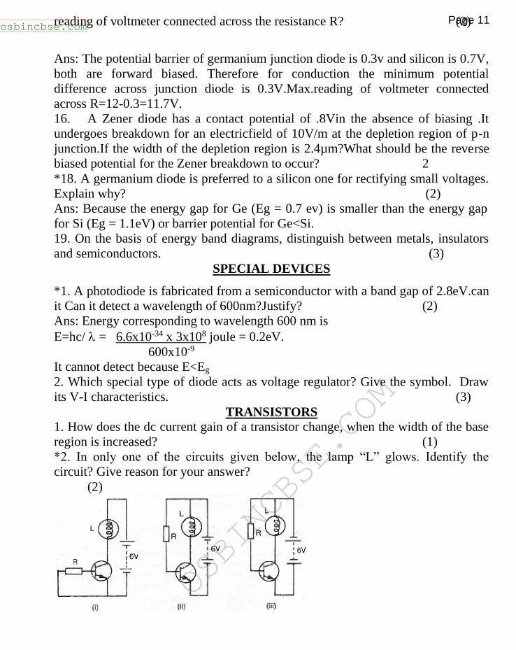
*2. In only one of the circuits given below, the lamp “L” glows. Identify the
circuit? Give reason for your answer?
(2)
Downloaded from www.studiestoday.com
Downloaded from www.studiestoday.com
osbincbse.com
OSBINCBSE.COM
OSBINCBSE.COM
OSBINCBSE.COM
Page 11
Ans: In fig (i) emitter –base junction has no source of emf. Therefore Ic =0, bulb
will not glow. In fig (ii) emitter – base junction is forward biased; therefore lamp
“L” will glow.
(iii) emitter – base junction is received biased so the bulb will not glow.
*3. Why do we prefer NPN transistor to PNP for faster action? (2)
Ans: For faster action NPN Transistor is used. In an NPN transistor, current
conduction is mainly by free electron, whereas in PNP type transistor, it is mainly
holes. Mobility of electrons is greater than that of holes.
4. In which mode, the cut off, active or saturation, the transistor is used as a
switch? Why? (2)
Ans: Cut off & saturation (deleted for March 2015)
5. In NPN transistor circuit, the collector current is 5mA. If 95% of the electrons
emitted reach the collector region, what is the base current? (2)
Here,
Ic=95% of Ie = (95 / 100 ) Ie
Ie = (100 / 95) × 5 mA = 5.26mA,
Ie=Ic+ Ib
Ib = 0.25 mA
6. A student has to study the input and output characteristics of a n-p-n silicon
transistor in the common emitter configuration. What kind of a circuit arrangement
should she use for this purpose? Draw the typical shape of input characteristics
likely to be obtained by that student.
(Ans: Fig 14.29, pg 493 & 494 NCERT-Part-2 physics
7. Which of input and output circuits of a transistor has a higher resistance and
why? (3)
Ans: The output circuit of a transistor has a higher resistance. Hint: The ratio of
resistance of output circuit (r0) is 104 times that of input circuit ie ro =104ri;
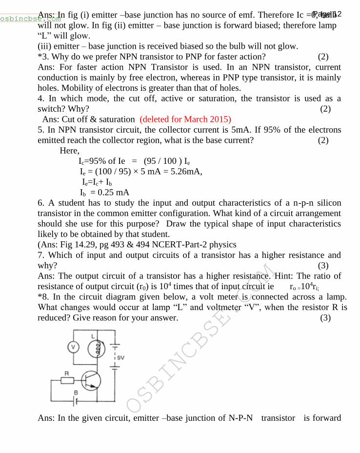
*8. In the circuit diagram given below, a volt meter is connected across a lamp.
What changes would occur at lamp “L” and voltmeter “V”, when the resistor R is
reduced? Give reason for your answer. (3)
Ans: In the given circuit, emitter –base junction of N-P-N transistor is forward
Downloaded from www.studiestoday.com
Downloaded from www.studiestoday.com
osbincbse.com
OSBINCBSE.COM
OSBINCBSE.COM
OSBINCBSE.COM
Page 12
biased.
When “R” decreases, IE increases. Because IC = IE – I B. Therefore IC will also
increase. Hence bulb will glow with more brightness and voltmeter reading will
increase.
9. The base current of a transistor is 105 µA and collector current is 2.05 mA. (3)
a) Determine the value of , Ie , and α
b) A change of 27 µA in the base current produces a change of 0.65 mA in the
collector current. Find a.c. Ib = 105 × 10 -
6A
Ic = 2.05 × 10 -
3A
= Ic / Ib
= 19.5
Also,
= 2.155 × 10 -
3
Ie = Ib +
Ic A
α = Ic / Ie = 0.95
Ib = 27µA = 27 × 10 -6 A
ac = Ic / Ib = 24.1
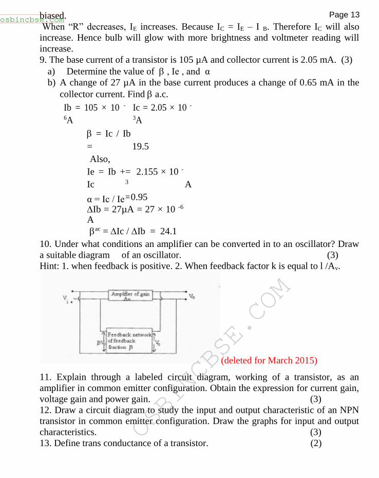
10. Under what conditions an amplifier can be converted in to an oscillator? Draw
a suitable diagram of an oscillator. (3)
Hint: 1. when feedback is positive. 2. When feedback factor k is equal to l /Av.
(deleted for March 2015)
11. Explain through a labeled circuit diagram, working of a transistor, as an
amplifier in common emitter configuration. Obtain the expression for current gain,
voltage gain and power gain. (3)
12. Draw a circuit diagram to study the input and output characteristic of an NPN
transistor in common emitter configuration. Draw the graphs for input and output
characteristics. (3)
13. Define trans conductance of a transistor. (2)
Downloaded from www.studiestoday.com
Downloaded from www.studiestoday.com
osbincbse.com
OSBINCBSE.COM
OSBINCBSE.COM
OSBINCBSE.COM
Page 13
Ans: gm = ∆IC/∆VB
14. How does the collector current change in junction transistor if the base region
has larger width?
Ans: Current decreases. (2)
15. The input of common emitter amplifier is 2KΏ. Current gain is 20. If the load
resistances is
5KΏ. Calculate voltage gain trans conductance.
(3)
Ans: gm = β / RI, Av = β RL/RI
16. Define input, output resistance, current amplification factor, voltage
amplification factor, for common emitter configuration of transistor. (3)
17. A change 0.2 mA in base current, causes a change of 5mA in collector current
in a common emitter amplifier.
(i) Find A.C current gain of Transistor.
(ii) If input resistance 2KΏ and voltage gain is 75. Calculate load resistance used in
circuit.
β AC current gain = β ∆Ic / ∆ Ib (3)
19. In a transistor the base current is changed by 20μA. This results in a change of
0.02V in base emitter voltage and a change of 2mA in collector current.
(i) Find input resistance, (3)
(ii) Trans conductance.
20. With the help of circuit diagram explain the action of a transistor. (3)
21. Draw the circuit diagram to study the characteristic of N-P-N transistor in
common emitter configuration. Sketch input – output characteristic for the
configuration. Explain current gain, voltage gain. (3)
22. Draw the transfer characteristics of a transistor in common emitter
configuration. Explain briefly the meaning of the term active region and cut off
region in this characteristic. (3)
23. Explain with the help of a circuit diagram the working of N-P-N transistor as a
common emitter amplifier. Draw input and output wave form. (3)
24. Draw a labeled circuit diagram of common emitter amplifier using P-N-P
transistor. Define voltage gain and write expression. Explain how the input and
output voltage are out of phase 180o for common emitter transistor amplifier.
(3)
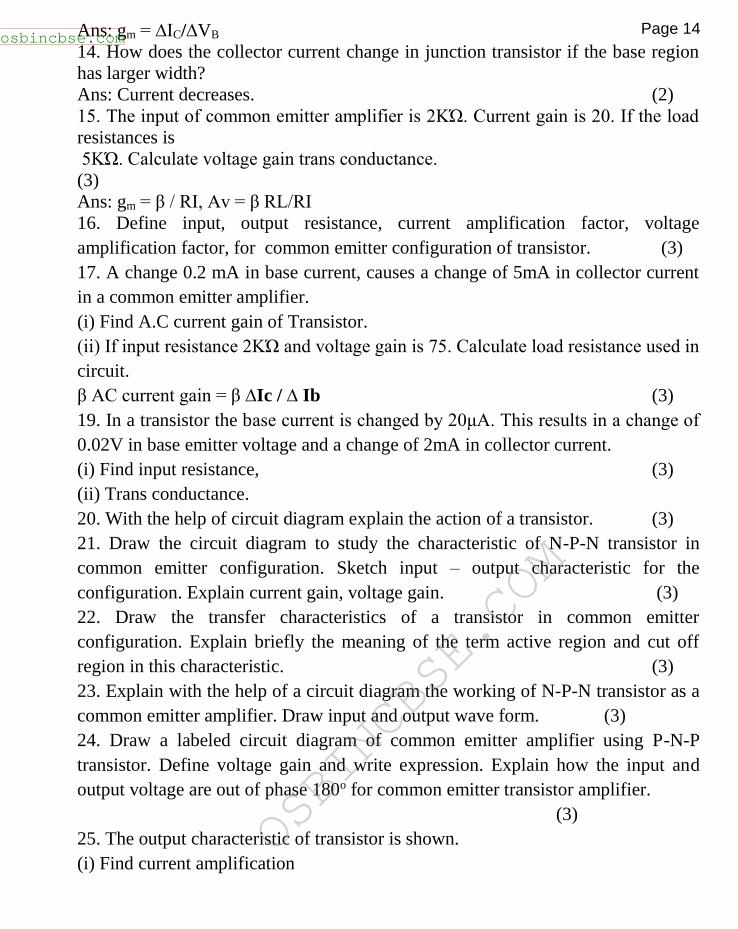
25. The output characteristic of transistor is shown.
(i) Find current amplification
Downloaded from www.studiestoday.com
Downloaded from www.studiestoday.com
osbincbse.com
OSBINCBSE.COM
OSBINCBSE.COM
OSBINCBSE.COM
Page 14
(ii) Output Resistance
Ic (mA)
0.5 1.0 1.5 2.0 2.5 3.0 3.5 4.0 VCE (V)
LOGIC GATES
*1. Modern technology use poly silicon instead of metal to form the gate. Why?
(1)
Ans: Poly silicon has high conductivity compared to metal.
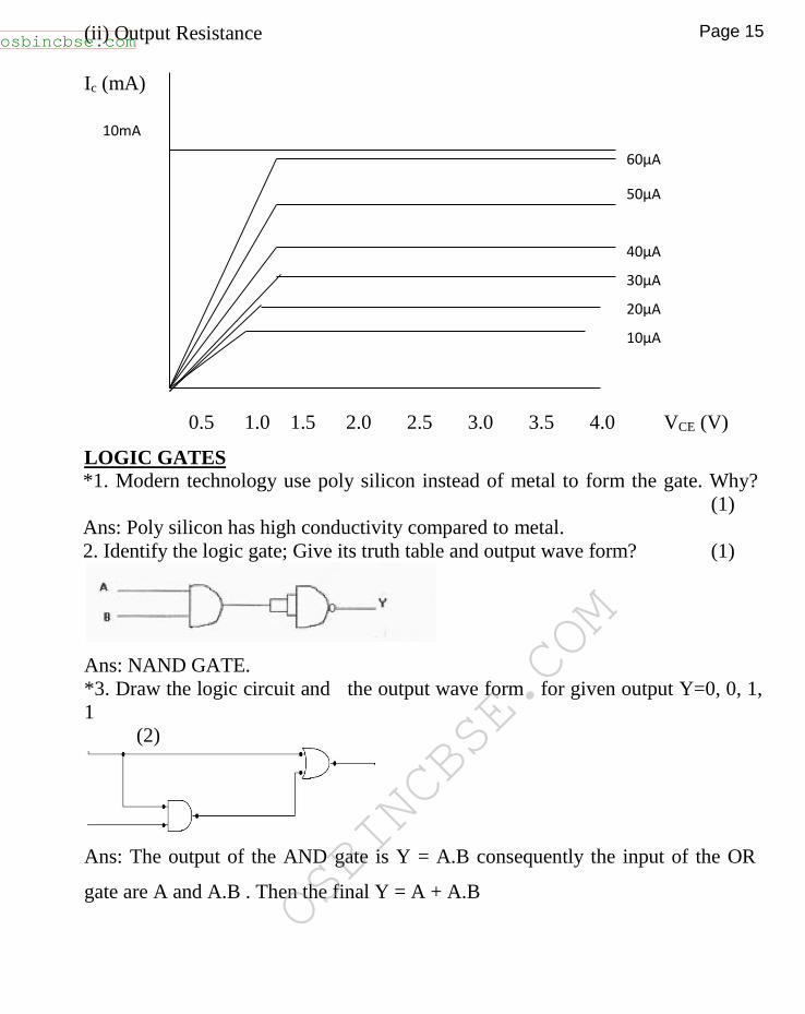
2. Identify the logic gate; Give its truth table and output wave form? (1)
Ans: NAND GATE.
*3. Draw the logic circuit and the output wave form for given output Y=0, 0, 1,
1
(2)
Ans: The output of the AND gate is Y = A.B consequently the input of the OR
gate are A and A.B . Then the final Y = A + A.B
10μA
20μA
30μA
40μA
50μA
60μA
10mA
Downloaded from www.studiestoday.com
Downloaded from www.studiestoday.com
osbincbse.com
OSBINCBSE.COM
OSBINCBSE.COM
OSBINCBSE.COM
Page 15
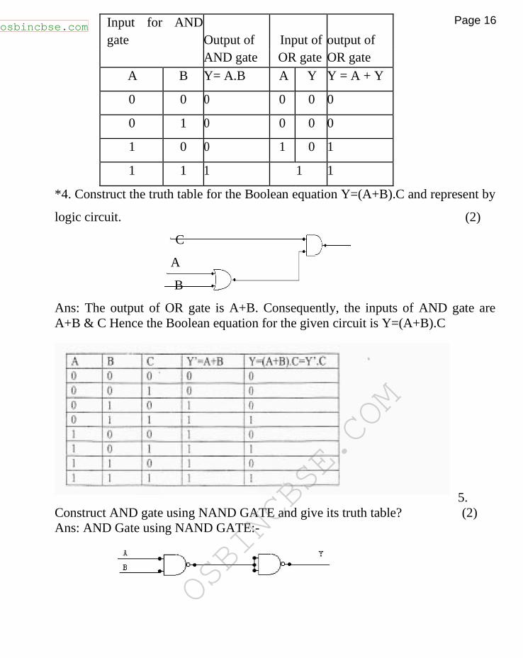
Input for AND
gate Output of Input of output of
AND gate OR gate OR gate
A B Y= A.B A Y Y = A + Y
0 0 0 0 0 0
0 1 0 0 0 0
1 0 0 1 0 1
1 1 1 1 1
*4. Construct the truth table for the Boolean equation Y=(A+B).C and represent by
logic circuit. (2)
C
Y
A
B
Ans: The output of OR gate is A+B. Consequently, the inputs of AND gate are
A+B & C Hence the Boolean equation for the given circuit is Y=(A+B).C
5.
Construct AND gate using NAND GATE and give its truth table? (2)
Ans: AND Gate using NAND GATE:-
Downloaded from www.studiestoday.com
Downloaded from www.studiestoday.com
osbincbse.com
OSBINCBSE.COM
OSBINCBSE.COM
OSBINCBSE.COM
Page 16
A B Y= A.B
0 0 0
0 1 0
1 0 0
1 1 1
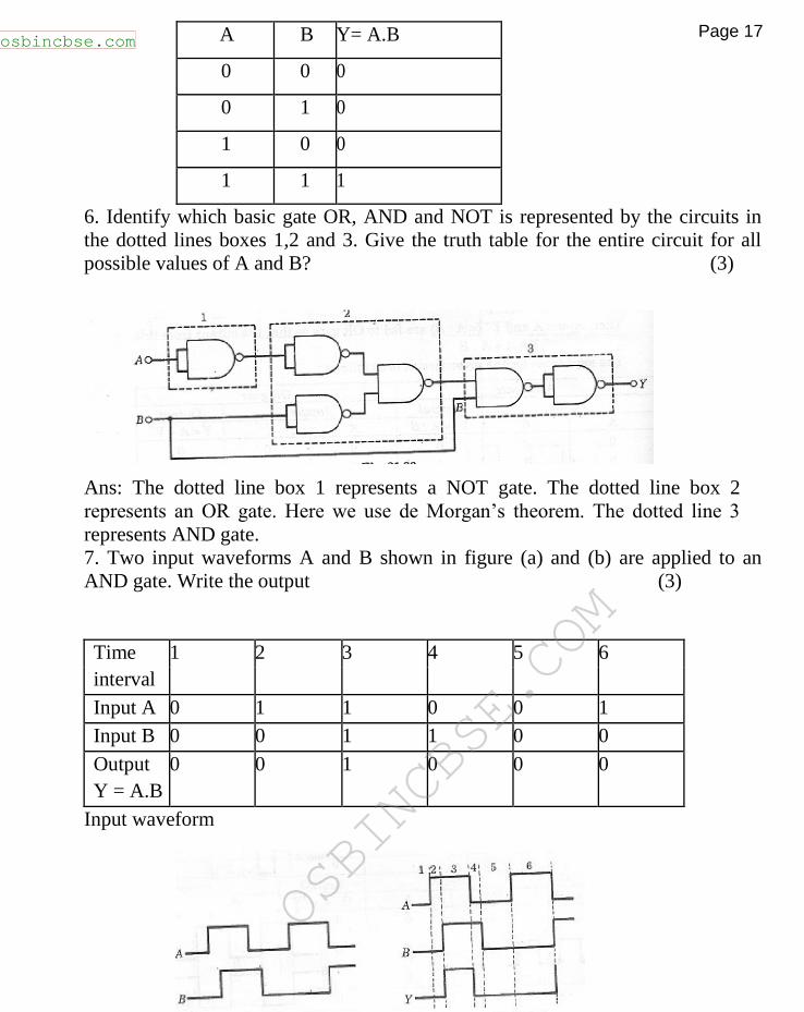
6. Identify which basic gate OR, AND and NOT is represented by the circuits in
the dotted lines boxes 1,2 and 3. Give the truth table for the entire circuit for all
possible values of A and B? (3)
Ans: The dotted line box 1 represents a NOT gate. The dotted line box 2
represents an OR gate. Here we use de Morgan’s theorem. The dotted line 3
represents AND gate.
7. Two input waveforms A and B shown in figure (a) and (b) are applied to an
AND gate. Write the output (3)
Time 1 2 3 4 5 6
interval
Input A 0 1 1 0 0 1
Input B 0 0 1 1 0 0
Output 0 0 1 0 0 0
Y = A.B
Input waveform
Downloaded from www.studiestoday.com
Downloaded from www.studiestoday.com
osbincbse.com
OSBINCBSE.COM
OSBINCBSE.COM
OSBINCBSE.COM
Page 17
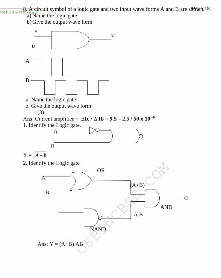
8. A circuit symbol of a logic gate and two input wave forms A and B are shown.
a) Name the logic gate
b) Give the output wave form
A
B
a. Name the logic gate
b. Give the output wave form
(3)
Ans: Current amplifier = ∆Ic / ∆ Ib = 9.5 – 2.5 / 50 x 10 -6
1. Identify the Logic gate.
A
B
Y = A B
2. Identify the Logic gate
OR
A
(A+B)
B
AND
A.B
NAND
Ans: Y = (A+B) AB
Downloaded from www.studiestoday.com
Downloaded from www.studiestoday.com
osbincbse.com
OSBINCBSE.COM
OSBINCBSE.COM
OSBINCBSE.COM
Page 18
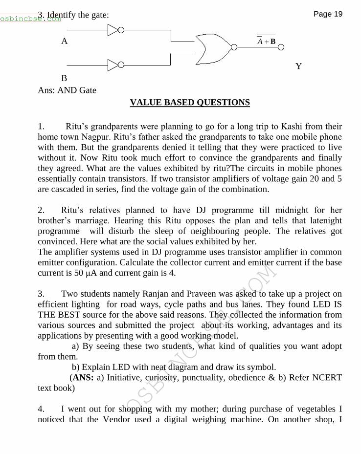
3. Identify the gate:
A A B
Y
B
Ans: AND Gate
VALUE BASED QUESTIONS
1. Ritu’s grandparents were planning to go for a long trip to Kashi from their
home town Nagpur. Ritu’s father asked the grandparents to take one mobile phone
with them. But the grandparents denied it telling that they were practiced to live
without it. Now Ritu took much effort to convince the grandparents and finally
they agreed. What are the values exhibited by ritu?The circuits in mobile phones
essentially contain transistors. If two transistor amplifiers of voltage gain 20 and 5
are cascaded in series, find the voltage gain of the combination.
2. Ritu’s relatives planned to have DJ programme till midnight for her
brother’s marriage. Hearing this Ritu opposes the plan and tells that latenight
programme will disturb the sleep of neighbouring people. The relatives got
convinced. Here what are the social values exhibited by her.
The amplifier systems used in DJ programme uses transistor amplifier in common
emitter configuration. Calculate the collector current and emitter current if the base
current is 50 μA and current gain is 4.
3. Two students namely Ranjan and Praveen was asked to take up a project on
efficient lighting for road ways, cycle paths and bus lanes. They found LED IS
THE BEST source for the above said reasons. They collected the information from
various sources and submitted the project about its working, advantages and its
applications by presenting with a good working model.
a) By seeing these two students, what kind of qualities you want adopt
from them.
b) Explain LED with neat diagram and draw its symbol.
(ANS: a) Initiative, curiosity, punctuality, obedience & b) Refer NCERT
text book)
4. I went out for shopping with my mother; during purchase of vegetables I
noticed that the Vendor used a digital weighing machine. On another shop, I
Downloaded from www.studiestoday.com
Downloaded from www.studiestoday.com
osbincbse.com
OSBINCBSE.COM
OSBINCBSE.COM
OSBINCBSE.COM
Page 19
noticed the vendor was using an ordinary weighing machine. So I used to go to the
shop with digital machine. I remembered having studied about Logic Gates where,
digital codes are used.
a) What do you mean by Logic Gate? Mention the basic universal gates.
b) What is the value, in your opinion, that I created by the above incident.
(ANS: a) –Refer NCERT Text book;
c) concentration and observation in the class room, retaining capacity, co-
relating of what was taught with the real life incident)
5. Arun and Naveen studying in KENDRIYA VIDYALAYA watched the
film “Swadesh” together getting inspiration from the film,they realized the need of
the hour for the conservation of energy. Together they decided to do something for
the nation. With the help of their school teachers and principal they arranged an
exhibition to depict the various renewable sources of energy and the applications
of it.
a) What values must have highlighted so that the youngsters are motivated?
b) Explain the working of a solar cell with a neat diagram.
(ANS: a) Need to conserve energy with the motto of sustainable development in
fulfilling the needs of the present generation without compromising the need of the
future generation, taking an initiative, bringing awareness among the students and
the society. (b) Refer NCERT text book)
6.Suraj was aware of the government policy regarding the supply of solar panels at
subsidised rates.During summer vacations ,when he reached his village to stay with
his grandparents for a fortnight,this idea struck him and persuaded his grandfather
to apply for solar panels. a. ) What are the values observed in Suraj? B.) Expain the
principle of working of solar cells
ANS: a.)progressive mentality,well versed with current affairs. B.)Refer the
NCERT text book.
7.Biju was learning about LED in his electronic class.He decided to make an LED
torch as a project. His instructor appreciated his efforts .He gifted this torch to his
grandmother. A.)What are the values observed in Biju? B.)Why is LED better
than normal torch bulb?
ANS: a.)Sharp,enthusiastic,applies the newly learnt knowledge for a beneficial
cause,care for elders. B.)Refer the NCERT text book.
Downloaded from www.studiestoday.com
Downloaded from www.studiestoday.com
osbincbse.com
OSBINCBSE.COM
OSBINCBSE.COM
OSBINCBSE.COM
Page 20
Recommended