8/19/2019 3. Arif Wahya Handoko_The Crystalline Structure, Conductivity and Optical Properties of Co-doped ZnO Thin Films
http://slidepdf.com/reader/full/3-arif-wahya-handokothe-crystalline-structure-conductivity-and-optical-properties 1/5
8/19/2019 3. Arif Wahya Handoko_The Crystalline Structure, Conductivity and Optical Properties of Co-doped ZnO Thin Films
http://slidepdf.com/reader/full/3-arif-wahya-handokothe-crystalline-structure-conductivity-and-optical-properties 2/5

8/19/2019 3. Arif Wahya Handoko_The Crystalline Structure, Conductivity and Optical Properties of Co-doped ZnO Thin Films
http://slidepdf.com/reader/full/3-arif-wahya-handokothe-crystalline-structure-conductivity-and-optical-properties 3/5
5866 S. Benramache et al. / Optik 125 (2014) 5864–5868
Fig.3. Thevariationof crystallitesize,the FWHMand theresidualstressof undoped
and Co-doped ZnOthin films with doping level.
tures [19,20]. The average crystallite sizeof the films fromthe XRD
was calculated using the Scherer’s equation [21]:
D =0.9
ˇ cos . (2)
where D is the crystallite size, is the X-ray wavelength
(=1.5406 A), ˇ is the full width at half-maximum (FWHM), and
is Bragg angle of (002) peak.According to thehexagonal symmetry of the ZnOstructure, the
lattice constant can be calculated by the following formula [22]:
dhk l =
4
3
h2+ hk+ k2
a2 +
l2
c 2
−1/2
. (3)
wherea, c arethelatticeparameters,(h,k, l) aretheMiller indices
of the planes and dhk l is the interplanar spacing.
Additional informationon structural properties canbe obtained
from the residual stressmeasurementscalculated by the following
formula [23].
= 450×c 0 − c
c . (4)
where in (GPa) is the mean stress, c and c 0 are the latticesconstant of the ZnO thin film and the bulk material (standard
c 0 = 0.5206nm). The calculated data of average mean stress issummarized in Table 1.
In Fig. 3 we have reported the variation of the crystallite size,
the full width-at-half-maximum (FWHM) and the residual stress
asa functionof dopinglevel. As itcan beseen, the variation of crys-
tallite size is opposite to the fullwidth-at-half-maximum(FWHM).
From 0 to 1wt%Co dopinglevels the crystallite size decreases from
63.99 to 29.61 nm (see Table 1) then increases to reach 59.42nm
as maximum value of 2 wt% and decreases further than the doping
level increase. Thevaluesof residual stressdecreaseswith increas-
ing of cobalt concentration from 0 to 1wt% then increases with
3wt% whereas the lattice parameter of the films decreases indi-
cating that the stress is done along the c -axis. The increase in thecrystallite size reveals the enhancement of the crystallinity under
c -axis orientation of ZnO thin films.
3.2. The optical properties of Co-doped ZnO thin films
Fig.4 showstheoptical transmissionspectraofundopedandCo-
doped ZnO as a function of doping level. As can be seen, a region
of strong transparency is located between 400–800nm; the value
of the average transmission is about 70–95%, then decreases in
the region of the absorption edge, in the layers (360–400nm) the
decrease is dueto thetransition between the valence band andthe
conduction band revealing the onset fundamental absorption. At
nakedeye,we arenotingthat thedopingeffectwasclearlyobserved
in the layer quality; hence the smoothness and homogeneityof the
Fig. 4. Transmission spectra of Co-doped ZnO thin films as a function of cobalt
concentration Co/Zn:(a) 0, (b) 1, (c) 2 and (d) 3wt%.
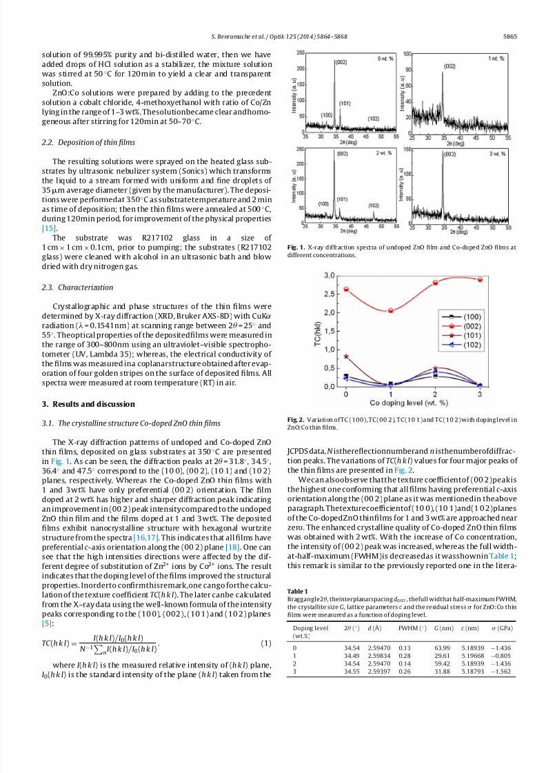
Fig. 5. The typical variation of ( Ahv)2 vs. photon energy hv for undoped ZnO thin
film. The inset shows the drawn of ln A as a function of photon energy (hv) for
deducing Urbachenergy.
layers reached an optimal state for theelaborated doped filmwith
2 wt%.
In order to investigate theeffectof Co concentration on ZnO:Cofilms further, the optical band gap energy (E g ) was measured from
the transmission spectra using the following relations [24]:
A = ˛d = − lnT, (5)
( Ah)2 = C (h − E g ), (6)
where A is theabsorbance,d is the filmthickness;T is the transmis-
sion spectra of thin films; ˛ is the absorption coefficient values; C
is a constant, h is the photon energy and E g the band gap energy
of the semiconductor. As it was shown in (Fig. 5) a typical varia-
tion of( Ah)2 as a function of photon energy (h) of undoped ZnO
thin film, the optical band gap was determined by extrapolation
of the linear region to (Ah)2 =0 [25]. Besides, we have used the
Urbachenergy (Table 2), which is related to the disorder in the filmnetwork and expressed as [15]:
A = A0 exp
h
E u
, (7)
Table 2
The band gap energy E g , the Urbach energy E u and electrical conductivity for
ZnO:Co thin films were measured as a function of doping level.
Doping level (wt%) E g (eV) E u (meV) ( cm)
0 3.367 085 7.71
1 3.278 267 7.19
2 3.319 040 8.33
3 3.295 166 7.86
8/19/2019 3. Arif Wahya Handoko_The Crystalline Structure, Conductivity and Optical Properties of Co-doped ZnO Thin Films
http://slidepdf.com/reader/full/3-arif-wahya-handokothe-crystalline-structure-conductivity-and-optical-properties 4/5
S. Benramache et al. / Optik 125 (2014) 5864–5868 5867
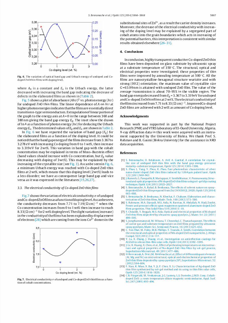
Fig. 6. The variation of optical band gap and Urbach energy of undoped and Co-
doped ZnOthin films with doping level.
where A0 is a constant and E u is the Urbach energy, the latter
decreased with increasing the band gap indicating the decrease of
defects in the elaborated films as shown in (Table 2).
Fig. 5 showsa plot of absorbance ( Ah)2 vs.photonenergy (h)
for undoped ZnO thin films. The linear dependence of A on h at
higherphotonenergiesindicates thatthefilmsareessentiallydirect
transitionn-type semiconductors. Extrapolationof linearportionof the graph to the energy axis at A= 0 in the range between 360 and
380 nm giving the band gap energy E g . The inset show the drawn
of ln A as a function of photon energy (hv) fordeducing the Urbach
energyE u. Thedetermined values of E g and E u are showninTable2.
In Fig. 6 we have reported the variation of band gap (E g ) for
the elaborated films as a function of the doping level. It could be
noticedthatthebandgapenergyof the filmsdecreasefrom 3.367to
3.278 eV with increasing Co doping from 0 to 1 wt%, then increase
to 3.319eV for 2wt%. This variation in band gap with the cobalt
concentration may be explained in terms of Moss–Burstein effect
(band values should increase with Co concentration, but E g value
decreasing with doping of 3wt%). This may be explained by the
increasing of thecrystallite size (see Fig. 3). Ascanbe seenin Fig. 6,
a minimum Urbach energy was reached with Co-doped ZnO thin
films at 2wt%, which means that this doping level (2wt%) leads to
a less disorder; we have as consequence large band gap and vice
versa as it was expressed in the literatures [15,26,27].
3.3. The electrical conductivity of Co-doped ZnO thin films
Fig.7 shows thevariationofelectricalconductivity ofundoped
andCo-dopedZnOfilmsasafunctionofdopinglevel.Ascanbeseen,
the conductivity decreases from 7.71 to 7.19( cm)−1 when the
Co concentration increases from 0 to 1wt% then increase to reach
8.33( cm)−1 for2 wt% dopinglevel. Theslight variation(increase)
in the conductivityof thefilmshas been explainedby displacement
of electrons[28] which arecoming from the ions Co2+ donorsin the
Fig. 7. Electrical conductivity ofundoped and Co-dopedZnO thinfilmsas a func-
tion of cobalt concentrations.
substitutional sites of Zn2+, as a result thecarrier density increases.
Moreover, thedecrease of the electrical conductivity with increas-
ing of the doping level may be explained by a segregated part of
cobalt atoms into the grain boundaries which acts in increasing of
the potential barriers, this interpretation is consistent with similar
results obtained elsewhere [26–31].
4. Conclusions
Inconclusion,highly transparentconductiveCo-dopedZnOthin
films have been deposited on glass substrate by ultrasonic spray
at a substrate temperature of 350 ◦C. The structural, optical and
electrical properties were investigated; these properties of thin
films were improved by annealing temperature at 500 ◦C. All the
films are nanocrystalline-hexagonal structure wurtzite and with
strong (00 2) orientation; the maximum value of crystallite size
G=63.99nm is attained with undoped ZnO film. The value of the
average transmission is about 70–95% in the visible region. The
band gap energydecreased from E g = 3.367 to3.319eV forundoped
andCo-doped ZnOthinfilmsat2wt%. Theelectrical conductivityof
thefilmsincreased from 7.71 to8.33 ( cm)−1. ImprovedCo-doped
ZnO films are achieved with 2wt% as amount of Co doping level.
Acknowledgments
This work was supported in part by the National Project
Research (PNR) andVTRS laboratory of El-OuedUniversity, Algeria.
X-ray diffraction data in this work were acquired with an instru-
ment supported by the University of Biskra. We thank Prof. S.
Rahman and B. Gasmi (Biskra Universty) for the assistance in XRD
data acquisition.
References
[1] S. Benramache, O. Belahssen, A. Arif, A. Guettaf, A correlation for crystal-l ite size of undoped ZnO thin film with the band gap energy–precursormolarity–substrate temperature, Optik 125 (2014)1303–1306.
[2] S. Zhao, L. Yang, Y. Zhou, K. Zhao, Fast photovoltaic characteristic of silvernano-cluster doped ZnO thin films induced by 1.064m pulsed laser, Optik122 (2011) 960–962.
[3] J. Ramesh,G. Pasupathi,R. Mariappan,V. SenthilKumar, V. Ponnuswamy,Struc-turaland optical properties ofNi dopedZnOthin films usingsol–geldipcoatingtechnique, Optik 124 (2013) 2023–2027.
[4] S. Benramache, A. Rahal, B. Benhaoua, The effects of solvent nature on spray-depositedZnO thin filmprepared from Zn(CH3COO)2, 2H2O, Optik 125(2014)663–666.
[5] S. Benramache, B. Benhaoua, N. Khechai, F. Chabane, Elaboration and charac-terization of ZnO thin films, Matér. Tech. 100 (2012) 573–580.
[6] S. Rahmane, M.A. Djouadi, M.S. Aida, N. Barreau, B. Abdallah, N. Hadj Zoubir,Power and pressure effects upon magnetron sputtered aluminum-doped ZnOfilms properties, Thin Solid Films 519 (2010) 5–10.
[7] F. Chouikh, Y. Beggah, M.S. Aida, Optical and electrical properties of Bi-dopedZnO thin films deposited by ultrasonic spray pyrolysis, J. Mater. Sci. 22 (2011)499–505.
[8] S. Jongthammanurak, M. Witana, T. Cheawkul, C. Thanachayanont, The effectsof carrier gas and substrate temperature on ZnO films prepared by ultrasonic
spray pyrolysis, Mater.Sci. Semicond. Process. 16 (2013) 625–632.[9] C. Ton-That, M. Foley, M.R. Phillips, T. Tsuzuki, Z. Smith, Correlation between
the structural and optical properties of Mn-doped ZnOnanoparticles, J. AlloysCompd. 522 (2012) 114–117.
[10] Y. Lu, X. Zhang, J. Huang, et al. , Investigation on antireflection coatings forAl:ZnO in silicon thin-film solar cells, Optik 124 (2013) 3392–3395.
[11] J. Lv, K. Huang, X. Chen, et al., Effect of preheating temperatureson microstruc-ture and optical properties of Na-doped ZnO thin films by sol–gel process,Superlattices Microstruct. 49 (2011)477–486.
[12] H.Benzarouk,A. Drici,M. Mekhnache,et al.,Effect of differentdopantelements(Al, Mg and Ni) on microstructural, optical and electrochemical properties of ZnO thin films depositedby spray pyrolysis(SP),Superlattices Microstruct. 52(2012) 594–604.
[13] F. Xian, K. Miao, X. Bai, Y. Ji, F. Chen, X. Li, Characteriaction of Ag-doped ZnOthin film synthesized by sol–gel method and its using in thin film solar cells,Optik 125 (2014) 1816–1820.
[14] C.B. Fitzgerald, M. Venkatesan, J.G. Lunney, L.S. Dorneles, J.M.D. Coey, Cobalt-doped ZnO: a room temperature dilute magnetic semiconductor, Appl. Surf.Sci. 247 (2005) 493–496.
8/19/2019 3. Arif Wahya Handoko_The Crystalline Structure, Conductivity and Optical Properties of Co-doped ZnO Thin Films
http://slidepdf.com/reader/full/3-arif-wahya-handokothe-crystalline-structure-conductivity-and-optical-properties 5/5
5868 S. Benramache et al. / Optik 125 (2014) 5864–5868
[15] S. Benramache, B. Benhaoua, Influence of annealing temperature on structuraland optical properties of ZnO: in thin films prepared by ultrasonic spray tech-nique, Superlattices Microstruct. 52 (2012)1062–1070.
[16] S. Benramache, B. Benhaoua, F. Chabane, A. Guettaf, A comparative study onthe nanocrystalline ZnO thin films prepared by ultrasonic spray and sol–gelmethod, Optik 124 (2013) 3221–3224.
[17] S. Benramache, B. Benhaoua, F. Chabane, F.Z. Lemadi, Influence of growth timeon crystalline structure, conductivity and optical properties of ZnO thin films, J. Semicond. 34 (2013) 023001–23004.
[18] A. Mhamdi, A. Boukhachem, M. Madani, H. Lachheb, K. Boubaker, A. Amlouk,M. Amlouk, Study of vanadium dopingeffects on structural, opto-thermal and
optical properties of sprayed ZnO semiconductor layers, Optik 124 (2013)3764–3770.
[19] L. Xu, X. Li, Y. Chena, F. Xu, Structural and optical properties of ZnO thin filmspreparedby sol–gelmethodwithdifferent thickness, Appl.Surf. Sci.257 (2011)4031–4037.
[20] A. Kalaivanan, S. Perumal, N.N. Pillai, K.R. Murali, Characteristics of GZO thinfilmsdeposited by sol–gel dipcoating, Mater. Sci. Semicond.Process. 14 (2011)94–96.
[21] P.Lv,L. Lin,W. Zheng, M. Zheng, F. Lai, Photosensitivity of ZnO/Cu2O thin filmheterojunction, Optik 124 (2013)2654–2657.
[22] M. Mazhdi, J. Saydi, M. Karimi, J. Seidi, F. Mazhdi, A study on optical, photolu-minescence and thermoluminescence properties of ZnO- and Mn-doped ZnOnanocrystalline particles, Optik 124 (2013)4128–4133.
[23] A.J.Hashim,M.S.Jaafar, J. Alaa,N.M. Ghazai, Ahmed, Fabrication and character-ization of ZnO thin film using sol–gel method, Optik 124 (2013) 491–492.
[24] S. Benramache, B. Benhaoua, Influence of substrate temperature and cobaltconcentration on structural and optical properties of ZnO thin films preparedby ultrasonicspray technique, Superlattices Microstruct. 52 (2012) 807–815.
[25] N. Karak, P.K. Samanta, T.K. Kundu, Green photoluminescence fromhighly ori-entedZnO thin filmfor photovoltaicapplication, Optik 124(2014) 6227–6230.
[26] S. Benramache, B.Benhaoua,F. Chabane,Effect of substratetemperatureon thestability of transparent conducting cobalt-doped ZnO thin films, J. Semicond.33 (2012)093001–93004.
[27] A. Hafdallah, F. Yanineb, M.S. Aida, N. Attaf, In doped ZnO thin films, J. Alloys
Compd. 509 (2011) 7267–7270.[28] H. Gomez, A. Maldonado, M. de la, L. Olvera, D.R. Acosta, Gallium-doped ZnO
thin films deposited by chemical spray, Sol. Energy Mater. Sol. Cells 87 (2005)107–116.
[29] A.Mosbah,M.S.Aida, Influenceof depositiontemperatureon structural, opticalandelectricalproperties of sputteredAl-dopedZnOthinfilms, J. AlloysCompd.515 (2012) 149–153.
[30] M.A.Lucio-López,M.A. Luna-Arias,A. Maldonado,M. dela, L.Olvera,D.R. Acosta,Preparation of conducting and transparent indium-doped ZnO thin films bychemical spray, Sol. Energy Mater.Sol. Cells 90 (2006) 733–741.
[31] A. Rahal, S. Benramache, B. Benhaoua, Preparation of n-type semiconductorSnO2 thin films, J. Semicond. 34 (2013) 083001–83011.
Recommended
![Optical and structural properties of Si-doped ZnO thin films...Si-doped ZnO nanocomposites [8–10] and nanorods [11]. In the present work we examine Si-doped ZnO thin films pro-](https://img.pdfslide.us/doc/110x75/610af404b2c50b3ec432d369/optical-and-structural-properties-of-si-doped-zno-thin-films-si-doped-zno-nanocomposites.jpg)
![The effect of SrTiO3 ZnO as cathodic buffer layer for ... · electron collecting ability, such as Al-doped ZnO (AZO), Ga-doped ZnO (GZO), and zinc tin oxide (ZTO) [43–45]. In this](https://img.pdfslide.us/doc/110x75/5f59c001a733ed7d5254d530/the-effect-of-srtio3-zno-as-cathodic-buffer-layer-for-electron-collecting-ability.jpg)