Datasheet 1.8" ZIF Solid State Drive WxZFxxxG1TC-E22xx Version 1.0
2/18/2014 www.wintecind.com
Page 1
1.8" ZIF PATA Solid State Drive EWS800
WxZFxxxG1TC-E22xx Series
INFORMATION IN THIS DOCUMENT IS PROVIDED IN RELATION TO WINTEC INDUSTRIES PRODUCTS, AND IS SUBJECT TO CHANGE WITHOUT NOTICE. NOTHING IN THIS DOCUMENT SHALL BE CONSTRUED AS GRANTING ANY LICENSE, EXPRESS OR IMPLIED. ALL INFORMATION IN THIS DOCUMENT IS PROVIDED ON AN “AS-IS” BASIS WITHOUT GUARANTEE OR WARRANTY OF ANY KIND.
Please contact your nearest Wintec representative for the latest updates or additional product information.
Datasheet 1.8" ZIF Solid State Drive WxZFxxxG1TC-E22xx Version 1.0
2/18/2014 www.wintecind.com
Page 2
Product Introduction Wintec 1.8" ZIF PATA Solid State Drive EWS800 Series W2ZFxxxG1TC-E22x The Wintec Industries EWS800 Series of RoHS compliant Solid State Drives are constructed with NAND-type flash memory devices paired to EWS800 SSD controller for virtual-to-physical address mapping and other sophisticated flash management functions. The Wintec Flash Solid State Drive (SSD) provides major advantages over the traditional magnetic hard disk drive (HDD). Faster access time and transfer rate, silent operation and low power consumption, better shock and vibration resistance, and lower total cost of ownership make the Wintec SSD’s and attractive choice as the next generation mass storage device. The EWS800 controller has the optimized hardware architecture to develop the efficient FTL (Flash Transition Layer) software and to provide the highest read/write performance. Also, the controller is compatible with the latest NAND Flash Interface (Asynchronous, Synchronous, and Toggle). The EWS800 series SSD provide high-speed data transfer and reliability utilizing SLC and MLC NAND Flash in storage capacities ranging from 32GB* - 512GB, in a small 1.8” ZIF form factor. Its robust design enables the SSD to achieve outstanding reliability and performance. Sequential reads at up to 120MB/s and sequential writes at up to 80MB/s are best in its class.
The EWS800 controller implements static and dynamic wear-leveling techniques and minimizes data write amplification to ensure that the NAND flash memory is not worn out prematurely. The controller utilizes up to 40-bit/1Kbyte sector BCH ECC per sector algorithms to ensure storage-data integrity between controller and NAND Flash device. Combining effective wear leveling management, and industrial temperature support, the Wintec EWS800 series SSD guarantees maximum reliability and longevity of the SSD.
*
Available capacities vary based on the Flash Type and drive configuration
General Features
Available densities of 32GB, 64GB, 128GB, 256GB
and 512GB ZIF IDE/ATA 40 pin interface
Slim form factor (71mm x 54mm x 5mm) High-speed ULTRA DMA
High-Performance SLC/MLC NAND Flash
8 to 10 channel internal parallelism
Disturbance Protection
Static and dynamic wear-leveling
Reliability
Hardware ECC Engine: Up to 40-bit BCH ECC per 1Kbyte and On-the-fly operation
MTTF: 2,000,000 operating hours
Performance (MLC)
Host transfer rate 150MB/s
Sequential Read 120MB/s
Sequential Write 80MB/s
Random Read: 5,000 IOPS at 4KB transfer
Random Write: 3,500 IOPS at 4KB transfer Compatibility
ATA-7 Stand Compliant:
- ATA/IDE 8-bit/16-bit parallel interface - Supports PIO Modes 0-4, Multiword DMA Modes 0-2 and Ultra DMA Modes 0-6 - Supports SMART feature set and 48-bit Address feature set
Pb free and RoHS compliant
Note:
1. See section 5.0 for configuration and Ordering Guide
Datasheet 1.8" ZIF Solid State Drive WxZFxxxG1TC-E22xx Version 1.0
2/18/2014 www.wintecind.com
Page 3
Revision History
Revision
Month
Year
History
1.0 February 2014 Initial release
Datasheet 1.8" ZIF Solid State Drive WxZFxxxG1TC-E22xx Version 1.0
2/18/2014 www.wintecind.com
Page 4
Table of Contents
1.0 General Product Specifications 5
1.1 Block Diagram 6
1.2 Architecture 7
1.3 Data compression and write amplification 7
1.4 Flash cell wear leveling 7
1.5 Error correction and data integrity 7
1.6 Block recycling and Garbage collection 7
1.7 TRIM Support 7
2.0 Electrical Specifications 8
2.1 DC Characteristics 8
2.2 PATA P in Assignment and Description 9
2.3 ATA - Register Transfer 10
2.4 ATA - PIO data transfer 12
2.5 ATA – Multiword DMA data Transfer 15
2.6 Initiating a Multiword DMA data burst 15
2.7 Sustaining a Multiword DMA data transfer 16
2.8 Device terminating a Multiword DMA data burst 16
2.9 Host terminating a Multiword DMA data burst 17
2.10 ATA – Ultra DMA data transfer 17
3.0 Software Interface 20
3.1 Supporting ATA Command Set of EWS800 20
3.2 ATA I/O Register Descriptions 20
4.0 Physical Specifications 21
4.1 Physical Specifications 21
5.0 Product Guide & Ordering Information 22
Datasheet 1.8" ZIF Solid State Drive WxZFxxxG1TC-E22xx Version 1.0
2/18/2014 www.wintecind.com
Page 5
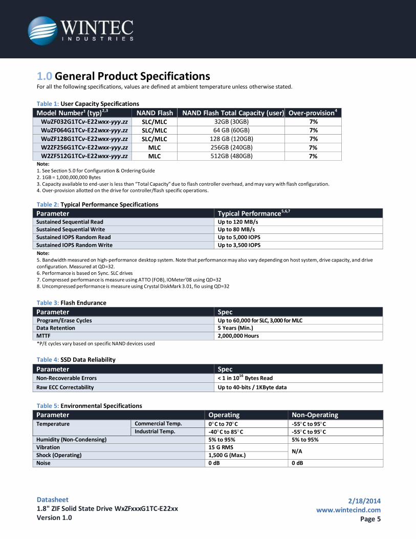
1.0 General Product Specifications For all the following specifications, values are defined at ambient temperature unless otherwise stated.
Table 1: User Capacity Specifications
Model Number¹ (typ)2,3 NAND Flash Type
NAND Flash Total Capacity (user) Over-provision4 WuZF032G1TCv-E22wxx-yyy.zz SLC/MLC 32GB (30GB) 7%
WuZF064G1TCv-E22wxx-yyy.zz SLC/MLC 64 GB (60GB) 7% WuZF128G1TCv-E22wxx-yyy.zz SLC/MLC 128 GB (120GB) 7% W2ZF256G1TCv-E22wxx-yyy.zz MLC 256GB (240GB) 7% W2ZF512G1TCv-E22wxx-yyy.zz MLC 512GB (480GB) 7%
Note: 1. See Section 5.0 for Configuration & Ordering Guide 2. 1GB = 1,000,000,000 Bytes 3. Capacity available to end-user is less than “Total Capacity” due to flash controller overhead, and may vary with flash configuration. 4. Over-provision allotted on the drive for controller/flash specific operations.
Table 2: Typical Performance Specifications
Parameter Typical Performance5,6,7 Sustained Sequential Read Up to 120 MB/s Sustained Sequential Write Up to 80 MB/s Sustained IOPS Random Read Up to 5,000 IOPS Sustained IOPS Random Write Up to 3,500 IOPS Note: 5. Bandwidth measured on high-performance desktop system. Note that performance may also vary depending on host system, drive capacity, and drive configuration. Measured at QD=32. 6. Performance is based on Sync. SLC drives 7. Compressed performance is measure using ATTO (FOB), IOMeter’08 using QD=32 8. Uncompressed performance is measure using Crystal DiskMark 3.01, fio using QD=32
Table 3: Flash Endurance
Parameter Spec Program/Erase Cycles Up to 60,000 for SLC, 3,000 for MLC Data Retention 5 Years (Min.) MTTF 2,000,000 Hours *P/E cycles vary based on specific NAND devices used
Table 4: SSD Data Reliability
Parameter Spec Non-Recoverable Errors < 1 in 10
16 Bytes Read
Raw ECC Correctability Up to 40-bits / 1KByte data
Table 5: Environmental Specifications
Parameter Operating Non-Operating Temperature Commercial Temp. 0C to 70C -55C to 95C
Industrial Temp. -40C to 85C -55C to 95C
Humidity (Non-Condensing) 5% to 95% 5% to 95% Vibration 15 G RMS
N/A Shock (Operating) 1,500 G (Max.) Noise 0 dB 0 dB
Datasheet 1.8" ZIF Solid State Drive WxZFxxxG1TC-E22xx Version 1.0
2/18/2014 www.wintecind.com
Page 6
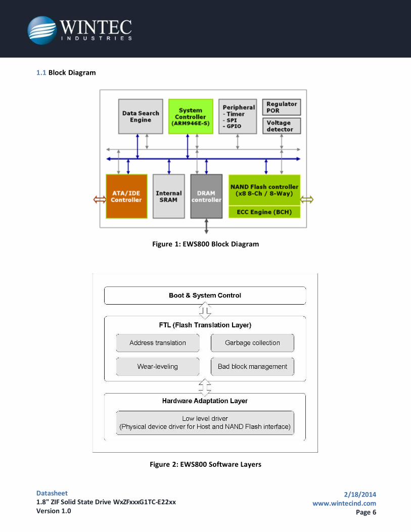
1.1 Block Diagram
Figure 1: EWS800 Block Diagram
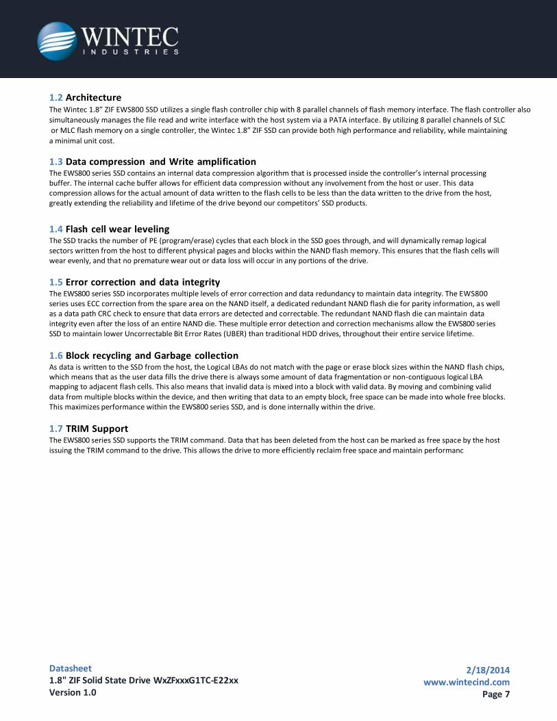
Figure 2: EWS800 Software Layers
Datasheet 1.8" ZIF Solid State Drive WxZFxxxG1TC-E22xx Version 1.0
2/18/2014 www.wintecind.com
Page 7
1.2 Architecture The Wintec 1.8” ZIF EWS800 SSD utilizes a single flash controller chip with 8 parallel channels of flash memory interface. The flash controller also
simultaneously manages the file read and write interface with the host system via a PATA interface. By utilizing 8 parallel channels of SLC
or MLC flash memory on a single controller, the Wintec 1.8” ZIF SSD can provide both high performance and reliability, while maintaining
a minimal unit cost.
1.3 Data compression and Write amplification The EWS800 series SSD contains an internal data compression algorithm that is processed inside the controller’s internal processing buffer. The internal cache buffer allows for efficient data compression without any involvement from the host or user. This data compression allows for the actual amount of data written to the flash cells to be less than the data written to the drive from the host, greatly extending the reliability and lifetime of the drive beyond our competitors’ SSD products.
1.4 Flash cell wear leveling The SSD tracks the number of PE (program/erase) cycles that each block in the SSD goes through, and will dynamically remap logical sectors written from the host to different physical pages and blocks within the NAND flash memory. This ensures that the flash cells will wear evenly, and that no premature wear out or data loss will occur in any portions of the drive.
1.5 Error correction and data integrity The EWS800 series SSD incorporates multiple levels of error correction and data redundancy to maintain data integrity. The EWS800 series uses ECC correction from the spare area on the NAND itself, a dedicated redundant NAND flash die for parity information, a s well as a data path CRC check to ensure that data errors are detected and correctable. The redundant NAND flash die can maintain data integrity even after the loss of an entire NAND die. These multiple error detection and correction mechanisms allow the EWS800 series SSD to maintain lower Uncorrectable Bit Error Rates (UBER) than traditional HDD drives, throughout their entire service lifetime.
1.6 Block recycling and Garbage collection As data is written to the SSD from the host, the Logical LBAs do not match with the page or erase block sizes within the NAND flash chips, which means that as the user data fills the drive there is always some amount of data fragmentation or non-contiguous logical LBA mapping to adjacent flash cells. This also means that invalid data is mixed into a block with valid data. By moving and combining valid data from multiple blocks within the device, and then writing that data to an empty block, free space can be made into whole free blocks. This maximizes performance within the EWS800 series SSD, and is done internally within the drive.
1.7 TRIM Support The EWS800 series SSD supports the TRIM command. Data that has been deleted from the host can be marked as free space by the host issuing the TRIM command to the drive. This allows the drive to more efficiently reclaim free space and maintain performanc
Datasheet 1.8" ZIF Solid State Drive WxZFxxxG1TC-E22xx Version 1.0
2/18/2014 www.wintecind.com
Page 8
2.0 Electrical Specifications
2.1 DC Characteristics
2.1.1 Absolute Maximum Ratings The absolute maximum ratings describe the conditions under which EWS800 will not be destroyed or suffer permanent damage.
Table 6: Absolute Maximum Ratings 3.0
Parameter Description Min Max Units Vcc - Vss VCC with respect to GND -0.5 4.8 V
2.1.2 Typical Operating Conditions
Table 7: Typical Operating Conditions 4.0
Parameter Description Min Max Units
VCC VCC with respect to GND 3.15 3.45 V
PI Idle Power Consumption 0.03 W
PA Active Power Consumption 0.5 W
PR Read Power Consumption 1.5 W
Pw Write Power Consumption 1.75 W
Datasheet 1.8" ZIF Solid State Drive WxZFxxxG1TC-E22xx Version 1.0
2/18/2014 www.wintecind.com
Page 9
2.2 PATA Pin Assignment and Description The PATA connectors are compliant with standard PATA power specifications.
Table 8: PATA connector specification compliant
Pin No Signal Name Pin No Signal Name 1 Reserved 2 Reserved
3 RESET- 4 GND
5 DD7 6 DD8
7 DD6 8 DD9
9 DD5 10 DD10
11 DD4 12 DD11
13 DD3 14 DD12
15 DD2 16 DD13
17 DD1 18 DD14
19 DD0 20 DD15
21 GND 22 DMARQ
23 GND 24 DIOW-:STOP
25 DIOR-:HDMARDY-:HSTROBE 26 GND
27 IOPRDY:DDMARDY-:DSTROBE 28 GND
29 DMACK- 30 INTR
31 DA 1 32 PDIAG-:CBLID-
33 DA 0 34 DA 2
35 CS0- 36 CS1-
37 DASP- 38 +3.3v
39 +3.3v 40 Reserved
2.3.1 Pin Locations
Figure 3: Pin Layout of ZIF Connectors - 40 pins
Datasheet 1.8" ZIF Solid State Drive WxZFxxxG1TC-E22xx Version 1.0
2/18/2014 www.wintecind.com
Page 10
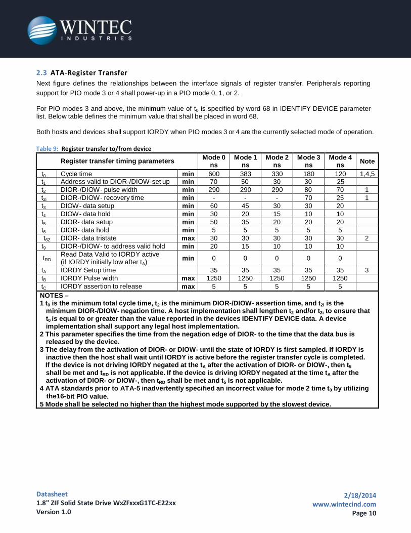
2.3 ATA-Register Transfer
Next figure defines the relationships between the interface signals of register transfer. Peripherals reporting
support for PIO mode 3 or 4 shall power-up in a PIO mode 0, 1, or 2.
For PIO modes 3 and above, the minimum value of t0 is specified by word 68 in IDENTIFY DEVICE parameter list. Below table defines the minimum value that shall be placed in word 68. Both hosts and devices shall support IORDY when PIO modes 3 or 4 are the currently selected mode of operation.
Table 9: Register transfer to/from device
Register transfer timing parameters Mode 0 ns
Mode 1 ns
Mode 2 ns
Mode 3 ns
Mode 4 ns
Note
t0 Cycle time min 600 383 330 180 120 1,4,5 t1 Address valid to DIOR-/DIOW-set up min 70 50 30 30 25 t2 DIOR-/DIOW- pulse width min 290 290 290 80 70 1 t2i DIOR-/DIOW- recovery time min - - - 70 25 1 t3 DIOW- data setup min 60 45 30 30 20 t4 DIOW- data hold min 30 20 15 10 10 t5 DIOR- data setup min 50 35 20 20 20 t6 DIOR- data hold min 5 5 5 5 5 t6Z DIOR- data tristate max 30 30 30 30 30 2
t9 DIOR-/DIOW- to address valid hold min 20 15 10 10 10
tRD Read Data Valid to IORDY active (if IORDY initially low after tA)
min 0 0 0 0 0
tA IORDY Setup time 35 35 35 35 35 3 tB IORDY Pulse width max 1250 1250 1250 1250 1250 tC IORDY assertion to release max 5 5 5 5 5 NOTES – 1 t0 is the minimum total cycle time, t2 is the minimum DIOR-/DIOW- assertion time, and t2i is the
minimum DIOR-/DIOW- negation time. A host implementation shall lengthen t2 and/or t2i to ensure that t0 is equal to or greater than the value reported in the devices IDENTIFY DEVICE data. A device implementation shall support any legal host implementation.
2 This parameter specifies the time from the negation edge of DIOR- to the time that the data bus is released by the device.
3 The delay from the activation of DIOR- or DIOW- until the state of IORDY is first sampled. If IORDY is inactive then the host shall wait until IORDY is active before the register transfer cycle is completed.
If the device is not driving IORDY negated at the tA after the activation of DIOR- or DIOW-, then t5
shall be met and tRD is not applicable. If the device is driving IORDY negated at the time tA after the activation of DIOR- or DIOW-, then tRD shall be met and t5 is not applicable.
4 ATA standards prior to ATA-5 inadvertently specified an incorrect value for mode 2 time t0 by utilizing the16-bit PIO value. 5 Mode shall be selected no higher than the highest mode supported by the slowest device.
Datasheet 1.8" ZIF Solid State Drive WxZFxxxG1TC-E22xx Version 1.0
2/18/2014 www.wintecind.com
Page 11
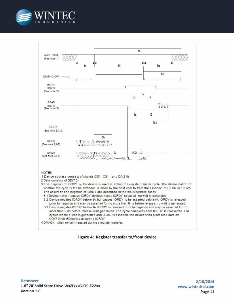
Figure 4: Register transfer to/from device
Datasheet 1.8" ZIF Solid State Drive WxZFxxxG1TC-E22xx Version 1.0
2/18/2014 www.wintecind.com
Page 12
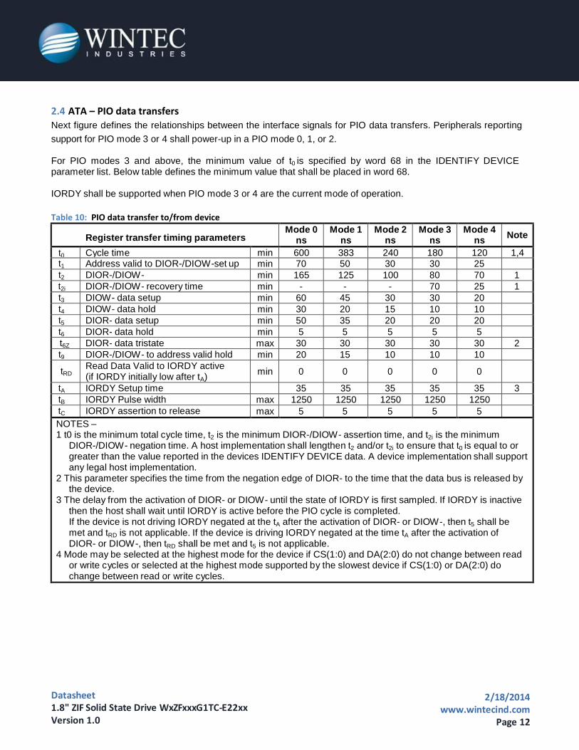
2.4 ATA – PIO data transfers
Next figure defines the relationships between the interface signals for PIO data transfers. Peripherals reporting
support for PIO mode 3 or 4 shall power-up in a PIO mode 0, 1, or 2. For PIO modes 3 and above, the minimum value of t0 is specified by word 68 in the IDENTIFY DEVICE parameter list. Below table defines the minimum value that shall be placed in word 68. IORDY shall be supported when PIO mode 3 or 4 are the current mode of operation.
Table 10: PIO data transfer to/from device
Register transfer timing parameters Mode 0
ns Mode 1
ns Mode 2
ns Mode 3
ns Mode 4
ns Note
t0 Cycle time min 600 383 240 180 120 1,4 t1 Address valid to DIOR-/DIOW-set up min 70 50 30 30 25 t2 DIOR-/DIOW- min 165 125 100 80 70 1 t2i DIOR-/DIOW- recovery time min - - - 70 25 1 t3 DIOW- data setup min 60 45 30 30 20 t4 DIOW- data hold min 30 20 15 10 10 t5 DIOR- data setup min 50 35 20 20 20 t6 DIOR- data hold min 5 5 5 5 5
t6Z DIOR- data tristate max 30 30 30 30 30 2 t9 DIOR-/DIOW- to address valid hold min 20 15 10 10 10
tRD Read Data Valid to IORDY active (if IORDY initially low after tA)
min 0 0 0 0 0
tA IORDY Setup time 35 35 35 35 35 3 tB IORDY Pulse width max 1250 1250 1250 1250 1250 tC IORDY assertion to release max 5 5 5 5 5 NOTES – 1 t0 is the minimum total cycle time, t2 is the minimum DIOR-/DIOW- assertion time, and t2i is the minimum
DIOR-/DIOW- negation time. A host implementation shall lengthen t2 and/or t2i to ensure that t0 is equal to or greater than the value reported in the devices IDENTIFY DEVICE data. A device implementation shall support any legal host implementation.
2 This parameter specifies the time from the negation edge of DIOR- to the time that the data bus is released by the device.
3 The delay from the activation of DIOR- or DIOW- until the state of IORDY is first sampled. If IORDY is inactive then the host shall wait until IORDY is active before the PIO cycle is completed. If the device is not driving IORDY negated at the tA after the activation of DIOR- or DIOW-, then t5 shall be met and tRD is not applicable. If the device is driving IORDY negated at the time tA after the activation of DIOR- or DIOW-, then tRD shall be met and t5 is not applicable.
4 Mode may be selected at the highest mode for the device if CS(1:0) and DA(2:0) do not change between read or write cycles or selected at the highest mode supported by the slowest device if CS(1:0) or DA(2:0) do change between read or write cycles.
Datasheet 1.8" ZIF Solid State Drive WxZFxxxG1TC-E22xx Version 1.0
2/18/2014 www.wintecind.com
Page 13
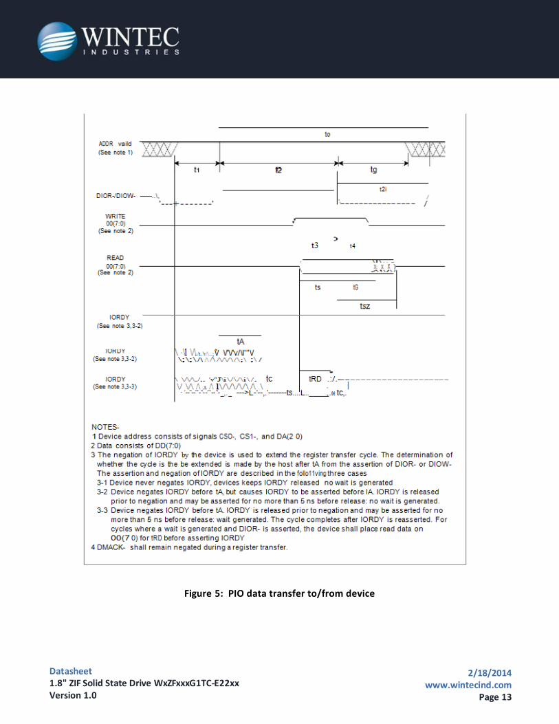
Figure 5: PIO data transfer to/from device
Datasheet 1.8" ZIF Solid State Drive WxZFxxxG1TC-E22xx Version 1.0
2/18/2014 www.wintecind.com
Page 14
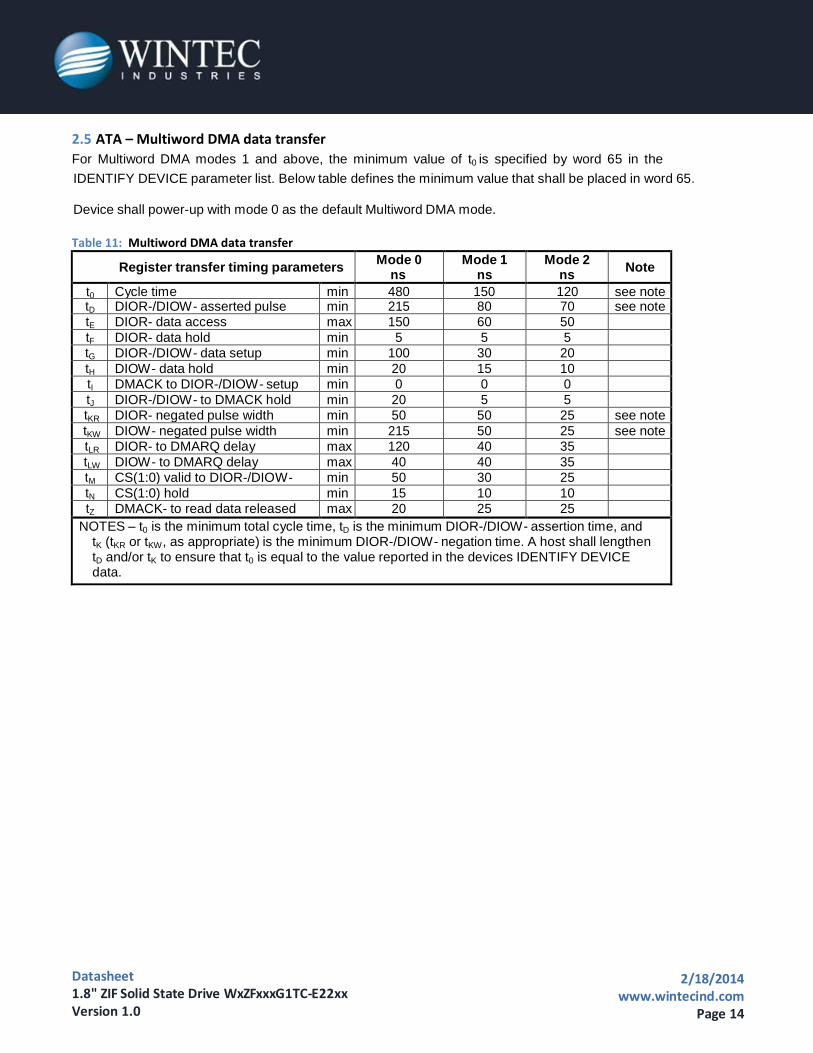
2.5 ATA – Multiword DMA data transfer
For Multiword DMA modes 1 and above, the minimum value of t0 is specified by word 65 in the
IDENTIFY DEVICE parameter list. Below table defines the minimum value that shall be placed in word 65.
Device shall power-up with mode 0 as the default Multiword DMA mode.
Table 11: Multiword DMA data transfer
Register transfer timing parameters Mode 0
ns Mode 1
ns Mode 2
ns Note
t0 Cycle time min 480 150 120 see note tD DIOR-/DIOW- asserted pulse
width min 215 80 70 see note
tE DIOR- data access max 150 60 50 tF DIOR- data hold min 5 5 5 tG DIOR-/DIOW- data setup min 100 30 20 tH DIOW- data hold min 20 15 10 tI DMACK to DIOR-/DIOW- setup min 0 0 0 tJ DIOR-/DIOW- to DMACK hold min 20 5 5 tKR DIOR- negated pulse width min 50 50 25 see note tKW DIOW- negated pulse width min 215 50 25 see note tLR DIOR- to DMARQ delay max 120 40 35 tLW DIOW- to DMARQ delay max 40 40 35 tM CS(1:0) valid to DIOR-/DIOW- min 50 30 25 tN CS(1:0) hold min 15 10 10 tZ DMACK- to read data released max 20 25 25
NOTES – t0 is the minimum total cycle time, tD is the minimum DIOR-/DIOW- assertion time, and tK (tKR or tKW, as appropriate) is the minimum DIOR-/DIOW- negation time. A host shall lengthen tD and/or tK to ensure that t0 is equal to the value reported in the devices IDENTIFY DEVICE data.
Datasheet 1.8" ZIF Solid State Drive WxZFxxxG1TC-E22xx Version 1.0
2/18/2014 www.wintecind.com
Page 15
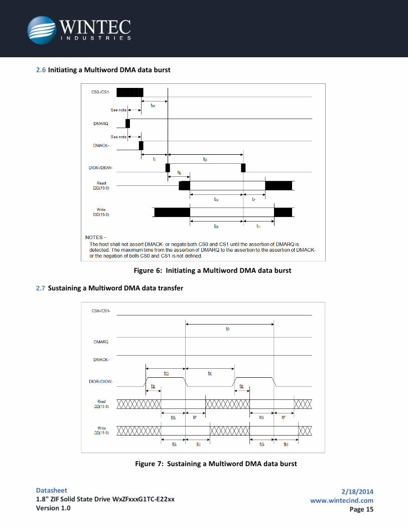
2.6 Initiating a Multiword DMA data burst
Figure 6: Initiating a Multiword DMA data burst
2.7 Sustaining a Multiword DMA data transfer
Figure 7: Sustaining a Multiword DMA data burst
Datasheet 1.8" ZIF Solid State Drive WxZFxxxG1TC-E22xx Version 1.0
2/18/2014 www.wintecind.com
Page 16
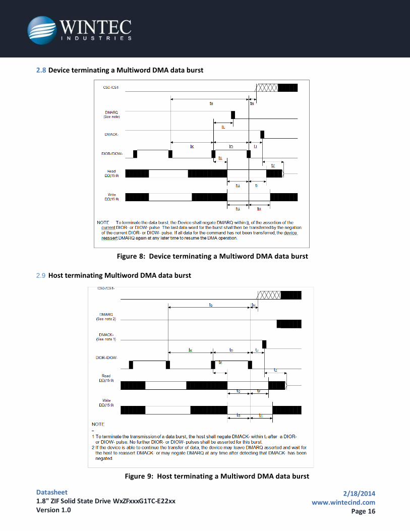
2.8 Device terminating a Multiword DMA data burst
Figure 8: Device terminating a Multiword DMA data burst
2.9 Host terminating Multiword DMA data burst
Figure 9: Host terminating a Multiword DMA data burst
Datasheet 1.8" ZIF Solid State Drive WxZFxxxG1TC-E22xx Version 1.0
2/18/2014 www.wintecind.com
Page 17
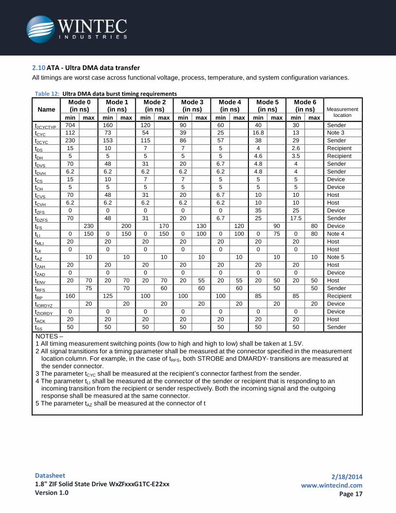
2.10 ATA - Ultra DMA data transfer
All timings are worst case across functional voltage, process, temperature, and system configuration variances.
Table 12: Ultra DMA data burst timing requirements
Name
Mode 0 (in ns)
Mode 1 (in ns)
Mode 2 (in ns)
Mode 3 (in ns)
Mode 4 (in ns)
Mode 5 (in ns)
Mode 6 (in ns)
Measurement location min max min max min max min max min max min max min max
t2CYCTYP 704 160 120 90 60 40 30 Sender tCYC 112 73 54 39 25 16.8 13 Note 3 t2CYC 230 153 115 86 57 38 29 Sender tDS 15 10 7 7 5 4 2.6 Recipient tDH 5 5 5 5 5 4.6 3.5 Recipient tDVS 70 48 31 20 6.7 4.8 4 Sender tDVH 6.2 6.2 6.2 6.2 6.2 4.8 4 Sender tCS 15 10 7 7 5 5 5 Device tCH 5 5 5 5 5 5 5 Device tCVS 70 48 31 20 6.7 10 10 Host tCVH 6.2 6.2 6.2 6.2 6.2 10 10 Host tZFS 0 0 0 0 0 35 25 Device tDZFS 70 48 31 20 6.7 25 17.5 Sender tFS 230 200 170 130 120 90 80 Device tLI 0 150 0 150 0 150 0 100 0 100 0 75 0 80 Note 4 tMLI 20 20 20 20 20 20 20 Host tUI 0 0 0 0 0 0 0 Host tAZ 10 10 10 10 10 10 10 Note 5 tZAH 20 20 20 20 20 20 20 Host tZAD 0 0 0 0 0 0 0 Device tENV 20 70 20 70 20 70 20 55 20 55 20 50 20 50 Host tRFS 75 70 60 60 60 50 50 Sender tRP 160 125 100 100 100 85 85 Recipient tIORDYZ 20 20 20 20 20 20 20 Device tZIORDY 0 0 0 0 0 0 0 Device tACK 20 20 20 20 20 20 20 Host tSS 50 50 50 50 50 50 50 Sender
NOTES – 1 All timing measurement switching points (low to high and high to low) shall be taken at 1.5V.
2 All signal transitions for a timing parameter shall be measured at the connector specified in the measurement location column. For example, in the case of tRFS, both STROBE and DMARDY- transitions are measured at the sender connector.
3 The parameter tCYC shall be measured at the recipient’s connector farthest from the sender. 4 The parameter tLI shall be measured at the connector of the sender or recipient that is responding to an
incoming transition from the recipient or sender respectively. Both the incoming signal and the outgoing response shall be measured at the same connector.
5 The parameter tAZ shall be measured at the connector of t
he sender or recipient that is driving the bus but must release the bus to allow for a bus turnaround.
Datasheet 1.8" ZIF Solid State Drive WxZFxxxG1TC-E22xx Version 1.0
2/18/2014 www.wintecind.com
Page 18
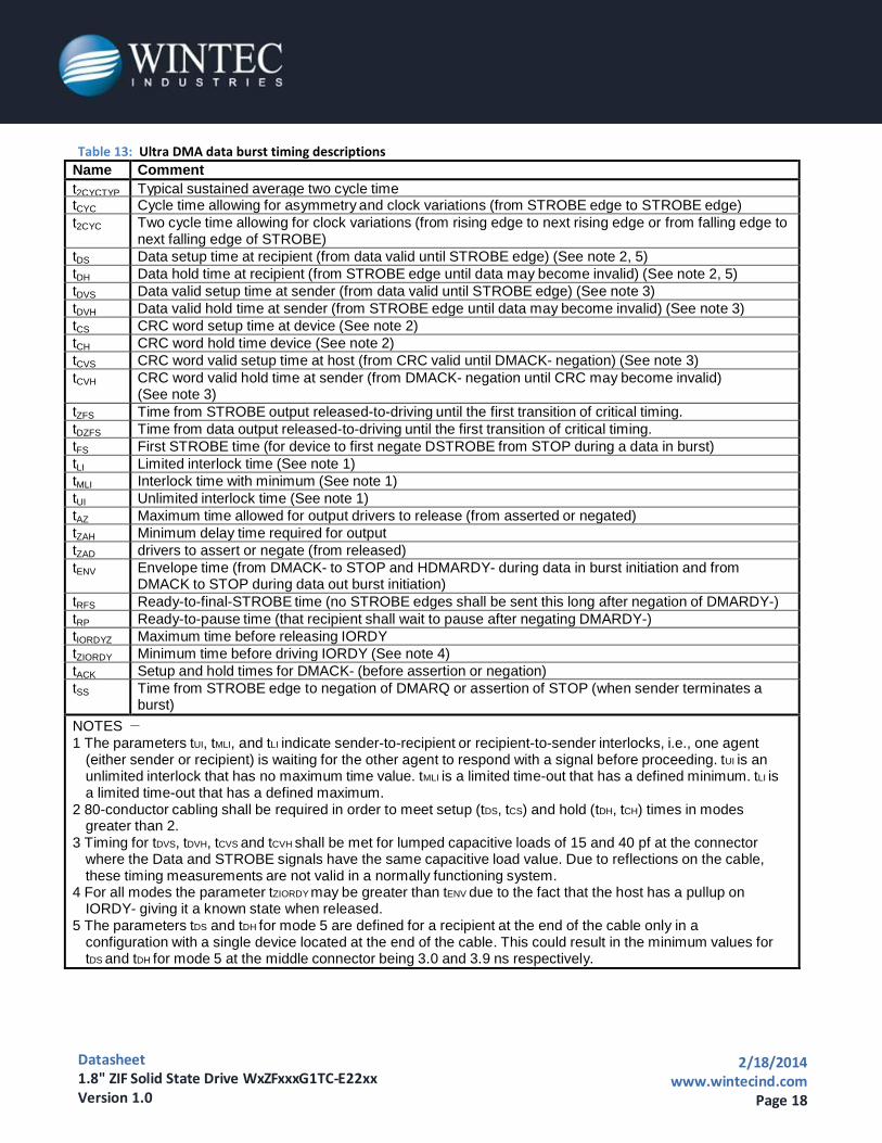
Table 13: Ultra DMA data burst timing descriptions
Name Comment t2CYCTYP Typical sustained average two cycle time tCYC Cycle time allowing for asymmetry and clock variations (from STROBE edge to STROBE edge) t2CYC Two cycle time allowing for clock variations (from rising edge to next rising edge or from falling edge to
next falling edge of STROBE) tDS Data setup time at recipient (from data valid until STROBE edge) (See note 2, 5) tDH Data hold time at recipient (from STROBE edge until data may become invalid) (See note 2, 5) tDVS Data valid setup time at sender (from data valid until STROBE edge) (See note 3) tDVH Data valid hold time at sender (from STROBE edge until data may become invalid) (See note 3) tCS CRC word setup time at device (See note 2) tCH CRC word hold time device (See note 2) tCVS CRC word valid setup time at host (from CRC valid until DMACK- negation) (See note 3) tCVH CRC word valid hold time at sender (from DMACK- negation until CRC may become invalid)
(See note 3) tZFS Time from STROBE output released-to-driving until the first transition of critical timing. tDZFS Time from data output released-to-driving until the first transition of critical timing. tFS First STROBE time (for device to first negate DSTROBE from STOP during a data in burst) tLI Limited interlock time (See note 1) tMLI Interlock time with minimum (See note 1) tUI Unlimited interlock time (See note 1) tAZ Maximum time allowed for output drivers to release (from asserted or negated) tZAH Minimum delay time required for output tZAD drivers to assert or negate (from released) tENV Envelope time (from DMACK- to STOP and HDMARDY- during data in burst initiation and from
DMACK to STOP during data out burst initiation) tRFS Ready-to-final-STROBE time (no STROBE edges shall be sent this long after negation of DMARDY-) tRP Ready-to-pause time (that recipient shall wait to pause after negating DMARDY-) tIORDYZ Maximum time before releasing IORDY tZIORDY Minimum time before driving IORDY (See note 4) tACK Setup and hold times for DMACK- (before assertion or negation) tSS Time from STROBE edge to negation of DMARQ or assertion of STOP (when sender terminates a
burst)
NOTES − 1 The parameters tUI, tMLI, and tLI indicate sender-to-recipient or recipient-to-sender interlocks, i.e., one agent
(either sender or recipient) is waiting for the other agent to respond with a signal before proceeding. tUI is an unlimited interlock that has no maximum time value. tMLI is a limited time-out that has a defined minimum. tLI is a limited time-out that has a defined maximum.
2 80-conductor cabling shall be required in order to meet setup (tDS, tCS) and hold (tDH, tCH) times in modes greater than 2.
3 Timing for tDVS, tDVH, tCVS and tCVH shall be met for lumped capacitive loads of 15 and 40 pf at the connector where the Data and STROBE signals have the same capacitive load value. Due to reflections on the cable, these timing measurements are not valid in a normally functioning system.
4 For all modes the parameter tZIORDY may be greater than tENV due to the fact that the host has a pullup on IORDY- giving it a known state when released.
5 The parameters tDS and tDH for mode 5 are defined for a recipient at the end of the cable only in a configuration with a single device located at the end of the cable. This could result in the minimum values for tDS and tDH for mode 5 at the middle connector being 3.0 and 3.9 ns respectively.
Datasheet 1.8" ZIF Solid State Drive WxZFxxxG1TC-E22xx Version 1.0
2/18/2014 www.wintecind.com
Page 19
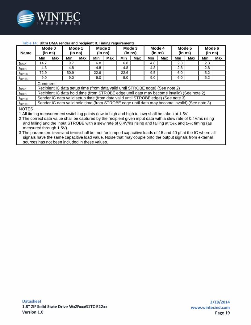
Table 14: Ultra DMA sender and recipient IC Timing requirements
Name
Mode 0 (in ns)
Mode 1 (in ns)
Mode 2 (in ns)
Mode 3 (in ns)
Mode 4 (in ns)
Mode 5 (in ns)
Mode 6 (in ns)
Min Max Min Max Min Max Min Max Min Max Min Max Min Max tDSIC 14.7 9.7 6.8 6.8 4.8 2.3 2.3 tDHIC 4.8 4.8 4.8 4.8 4.8 2.8 2.8 tDVSIC 72.9 50.9 22.6 22.6 9.5 6.0 5.2 tDVHIC 9.0 9.0 9.0 9.0 9.0 6.0 5.2
Comment tDSIC Recipient IC data setup time (from data valid until STROBE edge) (See note 2) tDHIC Recipient IC data hold time (from STROBE edge until data may become invalid) (See note 2) tDVSIC Sender IC data valid setup time (from data valid until STROBE edge) (See note 3) tDVHIC Sender IC data valid hold time (from STROBE edge until data may become invalid) (See note 3)
NOTES − 1 All timing measurement switching points (low to high and high to low) shall be taken at 1.5V. 2 The correct data value shall be captured by the recipient given input data with a slew rate of 0.4V/ns rising
and falling and the input STROBE with a slew rate of 0.4V/ns rising and falling at tDSIC and tDHIC timing (as measured through 1.5V).
3 The parameters tDVSIC and tDVHIC shall be met for lumped capacitive loads of 15 and 40 pf at the IC where all signals have the same capacitive load value. Noise that may couple onto the output signals from external sources has not been included in these values.
Datasheet 1.8" ZIF Solid State Drive WxZFxxxG1TC-E22xx Version 1.0
2/18/2014 www.wintecind.com
Page 20
3.0 Software Interface
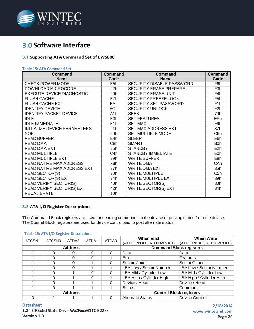
3.1 Supporting ATA Command Set of EWS800
Table 15: ATA Command Set
Command Name
Command Code
Command Name
Command Code
CHECK POWER MODE E5h SECURITY DISABLE PASSWORD F6h DOWNLOAD MICROCODE 92h SECURITY ERASE PREPARE F3h EXECUTE DEVICE DIAGNOSTIC 90h SECURITY ERASE UNIT F4h FLUSH CACHE E7h SECURITY FREEZE LOCK F5h FLUSH CACHE EXT EAh SECURITY SET PASSWORD F1h IDENTIFY DEVICE ECh SECURITY UNLOCK F2h IDENTIFY PACKET DEVICE A1h SEEK 70h IDLE E3h SET FEATURES EFh IDLE IMMEDIATE E1h SET MAX F9h INITIALIZE DEVICE PARAMETERS 91h SET MAX ADDRESS EXT 37h NOP 00h SET MULTIPLE MODE C6h READ BUFFER E4h SLEEP E6h READ DMA C8h SMART B0h READ DMA EXT 25h STANDBY E2h READ MULTIPLE C4h STANDBY IMMEDIATE E0h READ MULTIPLE EXT 29h WRITE BUFFER E8h READ NATIVE MAX ADDRESS F8h WRITE DMA CAh READ NATIVE MAX ADDRESS EXT 27h WRITE DMA EXT 35h READ SECTOR(S) 20h WRITE MULTIPLE C5h READ SECTOR(S) EXT 24h WRITE MULTIPLE EXT 39h READ VERIFY SECTOR(S) 40h WRITE SECTOR(S) 30h READ VERIFY SECTOR(S) EXT 42h WRITE SECTOR(S) EXT 34h RECALIBRATE 10h
3.2 ATA I/O Register Descriptions
The Command Block registers are used for sending commands to the device or posting status from the device. The Control Block registers are used for device control and to post alternate status.
Table 16: ATA I/O Register Descriptions
ATCSN1
ATCSN0
ATDA2
ATDA1
ATDA0 When read (ATDIORN = 0, ATDIOWN = 1)
When Write (ATDIORN = 1, ATDIOWN = 0)
Address Command Block registers 1 0 0 0 0 Data Data 1 0 0 0 1 Error Features 1 0 0 1 0 Sector Count Sector Count 1 0 0 1 1 LBA Low / Sector Number LBA Low / Sector Number 1 0 1 0 0 LBA Mid / Cylinder Low LBA Mid / Cylinder Low 1 0 1 0 1 LBA High / Cylinder High LBA High / Cylinder High 1 0 1 1 0 Device / Head Device / Head 1 0 1 1 1 Status Command
Address Control Block registers 0 1 1 1 0 Alternate Status Device Control
Datasheet 1.8" ZIF Solid State Drive WxZFxxxG1TC-E22xx Version 1.0
2/18/2014 www.wintecind.com
Page 21
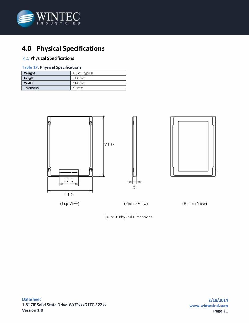
4.0 Physical Specifications 4.1 Physical Specifications
Table 17: Physical Specifications
Weight 4.0 oz. typical Length 71.0mm Width 54.0mm Thickness 5.0mm
(Top View) (Profile View) (Bottom View)
Figure 9: Physical Dimensions
Datasheet 1.8" ZIF Solid State Drive WxZFxxxG1TC-E22xx Version 1.0
2/18/2014 www.wintecind.com
Page 22
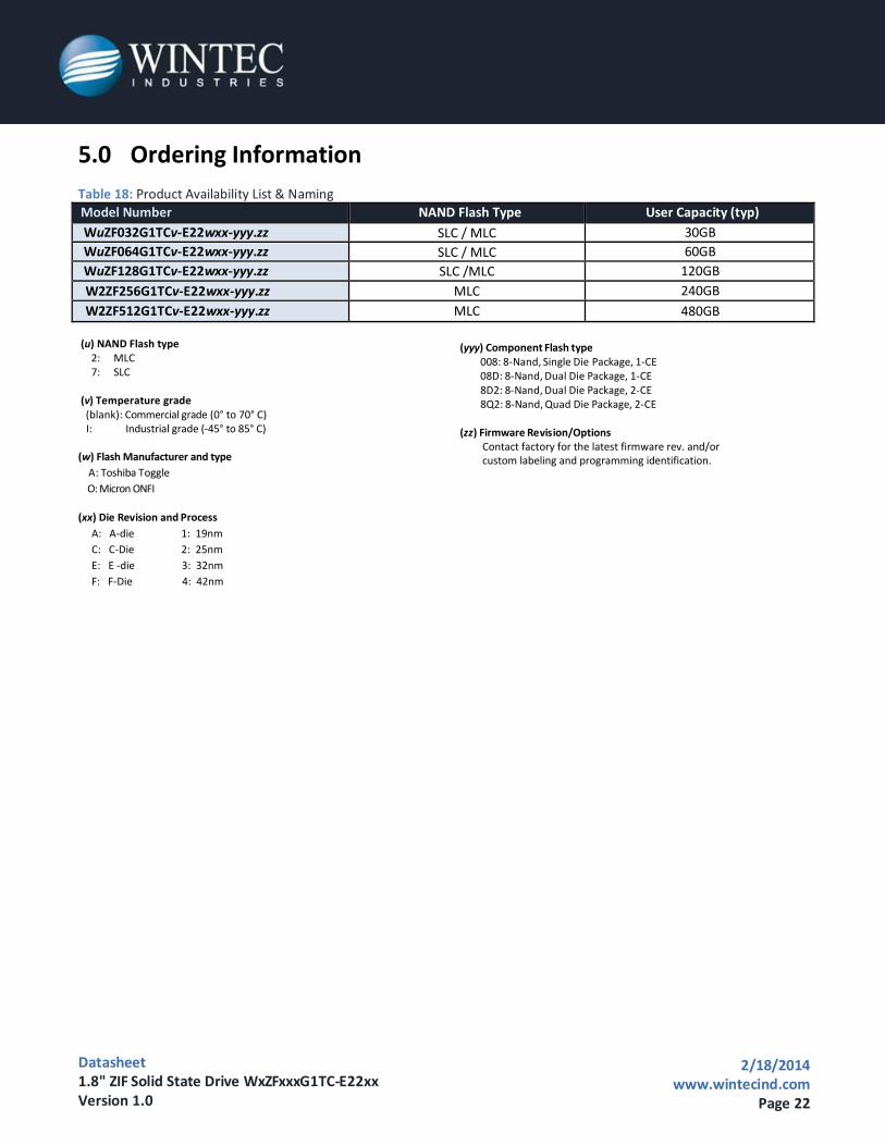
5.0 Ordering Information
Table 18: Product Availability List & Naming
Model Number NAND Flash Type User Capacity (typ) WuZF032G1TCv-E22wxx-yyy.zz SLC / MLC 30GB WuZF064G1TCv-E22wxx-yyy.zz SLC / MLC 60GB WuZF128G1TCv-E22wxx-yyy.zz SLC /MLC 120GB W2ZF256G1TCv-E22wxx-yyy.zz MLC 240GB
W2ZF512G1TCv-E22wxx-yyy.zz MLC 480GB
(u) NAND Flash type 2: MLC 7: SLC
(v) Temperature grade
(blank): Commercial grade (0° to 70° C) I: Industrial grade (-45° to 85° C)
(w) Flash Manufacturer and type
A: Toshiba Toggle
O: Micron ONFI
(xx) Die Revision and Process
A: A-die 1: 19nm
C: C-Die 2: 25nm
E: E -die 3: 32nm
F: F-Die 4: 42nm
(yyy) Component Flash type 008: 8-Nand, Single Die Package, 1-CE 08D: 8-Nand, Dual Die Package, 1-CE 8D2: 8-Nand, Dual Die Package, 2-CE 8Q2: 8-Nand, Quad Die Package, 2-CE
(zz) Firmware Revision/Options
Contact factory for the latest firmware rev. and/or custom labeling and programming identification.
Datasheet 1.8" ZIF Solid State Drive WxZFxxxG1TC-E22xx Version 1.0
2/18/2014 www.wintecind.com
Page 23
Contact Us (US & Int’l) Wintec Industries OEM Sales 675 Sycamore Drive Milpitas, CA 95035 Ph: 408-856-0500 Fax: 408-856-0501 [email protected] http://www.wintecind.com/oem
About Wintec Industries, Inc.: Wintec Industries, founded in 1988, is headquartered in Milpitas, California. Wintec, an ODM/OEM solution provider, specializes in product designs and manufacturing, including Flash modules (CF, SD, USB, embedded Flash, SSD, etc), DRAM modules (RDIMM, SODIMM, UDIMM), wireless products, modem products (embedded and USB), Advanced Digital Display products (ADD2 DVI, HDMI, digital signage), and so on. With experienced engineering team in Silicon Valley, Wintec provides a wide range of services and solutions for customers. Wintec is ISO9001-2000 certified.
Important Notice:
Wintec Industries makes no representations or warranties with respect to the contents of this datasheet and specifically disclaims any implied warranties of any product design for any particular purpose. Wintec Industries reserves the rights to revise this publication and to make changes from time to time in the content hereof without obligation of Wintec Industries to notify any person or organization of such revisions or changes.
Recommended