15EE209L-ANALOG AND DIGITAL CIRCUITS LAB
1
15EE209L-ANALOG AND DIGITAL CIRCUITS LAB
RECORD
ACADEMIC YEAR: 2017-18
NAME :
REG.NO. :
DEPARTMENT OF ELECTRICAL & ELECTRONICS ENGINEERING
FACULTY OF ENGINEERING & TECHNOLOGY SRM UNIVERSITY
(Under section 3 of UGC Act, 1956) S.R.M. NAGAR, KATTANKULATHUR – 603 203
KANCHEEPURAM DISTRICT
15EE209L-ANALOG AND DIGITAL CIRCUITS LAB
2
SRM UNIVERSITY (under Section 3 of UGC Act, 1956)
S.R.M. NAGAR, KATTANKULATHUR -603 203 KANCHEEPURAM DISTRICT
BONAFIDE CERTIFICATE
Register No__________________
Certified to be the bonafide record of work done by
________________________ of EEE, B.Tech Degree course in the
Practical 15EE209L Analog and Digital Circuits Lab in SRM
UNIVERSITY, Kattankulathur during the academic year 2017-2018
Lab In charge
Date: Year Coordinator
Submitted for University Examination held in …. ………………………………, SRM UNIVERSITY, Kattankulathur.
Date: Examiner-1 Examiner-2
15EE209L-ANALOG AND DIGITAL CIRCUITS LAB
3
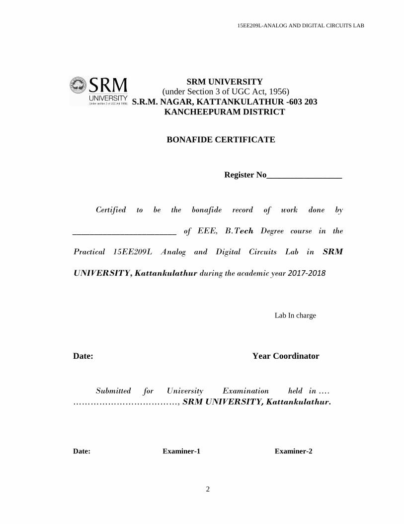
INDEX
Sl.NO D.O.E Title of Experiment D.O.S Marks Signature
1 Characteristics of BJT and FET
2 Half wave Rectifier and Full Wave rectifier
3 Clippers and Clampers
4 Design of RC Phase Shift Oscillator
5 Frequency response of voltage series feedback amplifier
6 Adders, Subtractors and Flip-Flops
7 Design of Multiplexer and De-multiplexer
8 Design of Counters
9 PSpice simulation of BJT and FET characteristics
10 Design of Digital logic circuits using VHDL
15EE209L-ANALOG AND DIGITAL CIRCUITS LAB
4
DEPT. OF ELECTRICAL & ELECTRONICS ENGINEERING SRM UNIVERSITY, Kattankulathur – 603203.
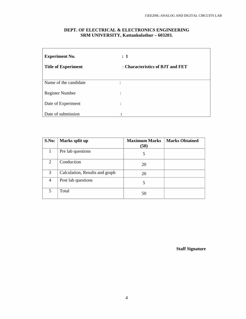
Experiment No. : 1 Title of Experiment : Characteristics of BJT and FET Name of the candidate : Register Number : Date of Experiment : Date of submission : S.No: Marks split up Maximum Marks
(50) Marks Obtained
1 Pre lab questions 5
2 Conduction 20
3 Calculation, Results and graph 20
4 Post lab questions 5
5 Total 50
Staff Signature

15EE209L-ANALOG AND DIGITAL CIRCUITS LAB
5
1. Characteristics of BJT and FET
Pre Lab Questions
1. When does a transistor act as an amplifier?
2. What are the types of configuration in a transistor?
3. Why h-parameters are called as hybrid parameters?
4. What is mutual conductance?
5. Define current gain and voltage gain
6. Why FET is called a Unipolar device?
15EE209L-ANALOG AND DIGITAL CIRCUITS LAB
6
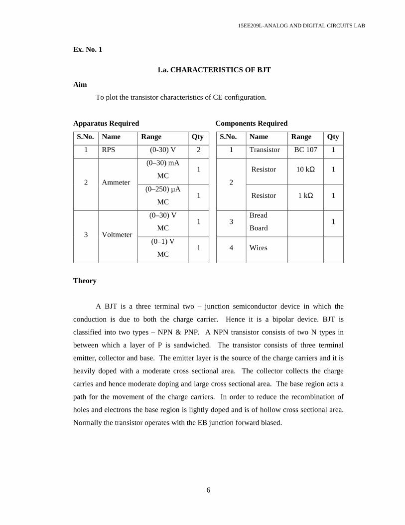
Ex. No. 1
1.a. CHARACTERISTICS OF BJT
Aim
To plot the transistor characteristics of CE configuration.
Apparatus Required Components Required
S.No. Name Range Qty
S.No. Name Range Qty
1 RPS (0-30) V 2 1 Transistor BC 107 1
2 Ammeter
(0–30) mA
MC 1
2
Resistor 10 kΩ 1
(0–250) µA
MC 1 Resistor 1 kΩ 1
3 Voltmeter
(0–30) V
MC 1 3
Bread
Board 1
(0–1) V
MC 1 4 Wires
Theory
A BJT is a three terminal two – junction semiconductor device in which the
conduction is due to both the charge carrier. Hence it is a bipolar device. BJT is
classified into two types – NPN & PNP. A NPN transistor consists of two N types in
between which a layer of P is sandwiched. The transistor consists of three terminal
emitter, collector and base. The emitter layer is the source of the charge carriers and it is
heavily doped with a moderate cross sectional area. The collector collects the charge
carries and hence moderate doping and large cross sectional area. The base region acts a
path for the movement of the charge carriers. In order to reduce the recombination of
holes and electrons the base region is lightly doped and is of hollow cross sectional area.
Normally the transistor operates with the EB junction forward biased.
15EE209L-ANALOG AND DIGITAL CIRCUITS LAB
7
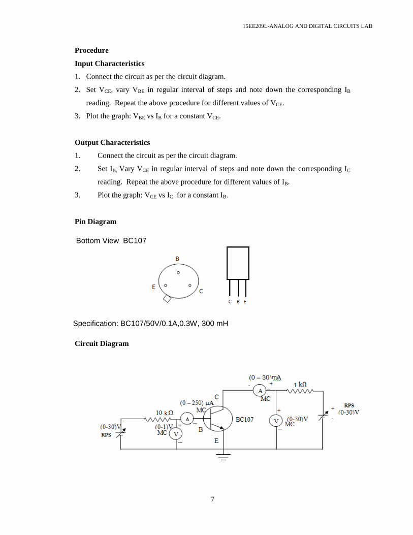
Bottom View BC107
Specification: BC107/50V/0.1A,0.3W, 300 mH
Procedure
Input Characteristics
1. Connect the circuit as per the circuit diagram.
2. Set VCE, vary VBE in regular interval of steps and note down the corresponding IB
reading. Repeat the above procedure for different values of VCE.
3. Plot the graph: VBE vs IB for a constant VCE.
Output Characteristics
1. Connect the circuit as per the circuit diagram.
2. Set IB, Vary VCE in regular interval of steps and note down the corresponding IC
reading. Repeat the above procedure for different values of IB.
3. Plot the graph: VCE vs IC for a constant IB.
Pin Diagram
Circuit Diagram
15EE209L-ANALOG AND DIGITAL CIRCUITS LAB
8
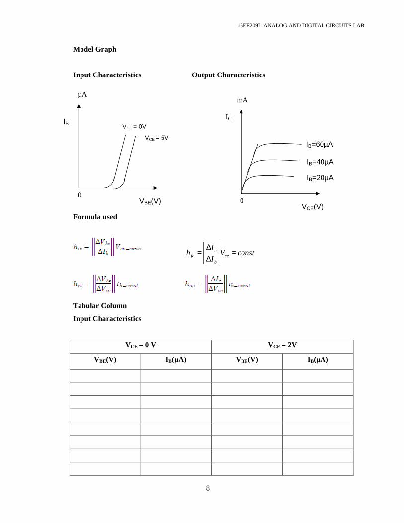
Model Graph
Input Characteristics Output Characteristics
Formula used
constVI
Ih ce
b
cfe =
∆∆
=
Tabular Column
Input Characteristics
VCE = 0 V VCE = 2V
VBE(V) I B(µA) VBE(V) I B(µA)
VCE = 0V
VCE = 5V
IB
µA mA
VBE(V) VCE(V)
0 0
IB=60µA
IB=40µA
IB=20µA
IC

15EE209L-ANALOG AND DIGITAL CIRCUITS LAB
9
Output Characteristics
IB=20µµµµA I B=40µµµµA
VCE(V) I C(mA) VCE(V) I C(mA)
15EE209L-ANALOG AND DIGITAL CIRCUITS LAB
10
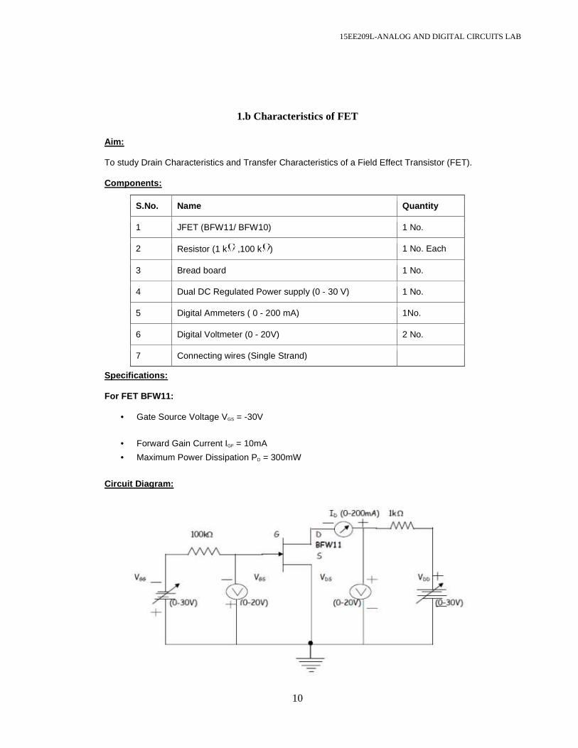
1.b Characteristics of FET
Aim:
To study Drain Characteristics and Transfer Characteristics of a Field Effect Transistor (FET).
Components:
S.No. Name Quantity
1 JFET (BFW11/ BFW10) 1 No.
2 Resistor (1 k ,100 k ) 1 No. Each
3 Bread board 1 No.
4 Dual DC Regulated Power supply (0 - 30 V) 1 No.
5 Digital Ammeters ( 0 - 200 mA) 1No.
6 Digital Voltmeter (0 - 20V) 2 No.
7 Connecting wires (Single Strand)
Specifications:
For FET BFW11:
• Gate Source Voltage VGS = -30V
• Forward Gain Current IGF = 10mA
• Maximum Power Dissipation PD = 300mW
Circuit Diagram:
15EE209L-ANALOG AND DIGITAL CIRCUITS LAB
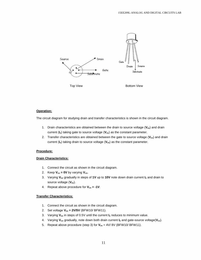
11
Top View Bottom View
Operation:
The circuit diagram for studying drain and transfer characteristics is shown in the circuit diagram.
1. Drain characteristics are obtained between the drain to source voltage (VDS) and drain
current (ID) taking gate to source voltage (VGS) as the constant parameter.
2. Transfer characteristics are obtained between the gate to source voltage (VGS) and drain
current (ID) taking drain to source voltage (VDS) as the constant parameter.
Procedure:
Drain Characteristics:
1. Connect the circuit as shown in the circuit diagram.
2. Keep VGS = 0V by varying VGG.
3. Varying VDD gradually in steps of 1V up to 10V note down drain current ID and drain to
source voltage (VDS).
4. Repeat above procedure for VGS = -1V.
Transfer Characteristics:
1. Connect the circuit as shown in the circuit diagram.
2. Set voltage VDS = 2V/5V (BFW10/ BFW11).
3. Varying VDD in steps of 0.5V until the current ID reduces to minimum value.
4. Varying VGG gradually, note down both drain current ID and gate-source voltage(VGS).
5. Repeat above procedure (step 3) for VDS = 4V/ 8V (BFW10/ BFW11).
15EE209L-ANALOG AND DIGITAL CIRCUITS LAB
12
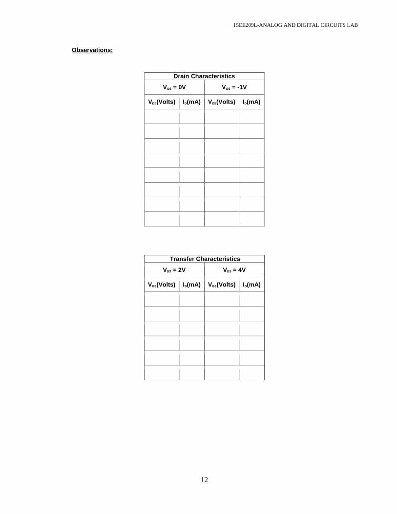
Observations:
Drain Characteristics
VGS = 0V VGS = -1V
VDS(Volts) ID(mA) VDS(Volts) ID(mA)
Transfer Characteristics
VDS = 2V VDS = 4V
VGS(Volts) ID(mA) VGS(Volts) ID(mA)
15EE209L-ANALOG AND DIGITAL CIRCUITS LAB
13
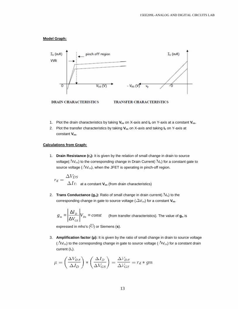
Model Graph:
1. Plot the drain characteristics by taking VDS on X-axis and ID on Y-axis at a constant VGS.
2. Plot the transfer characteristics by taking VGS on X-axis and taking ID on Y-axis at
constant VDS.
Calculations from Graph:
1. Drain Resistance (r d): It is given by the relation of small change in drain to source
voltage( VDS) to the corresponding change in Drain Current( ID) for a constant gate to
source voltage ( VGS), when the JFET is operating in pinch-off region.
at a constant VGS (from drain characteristics)
2. Trans Conductance (g m): Ratio of small change in drain current( ID) to the
corresponding change in gate to source voltage ( VGS) for a constant VDS.
constVV
Ig Ds
GS
Dm =
∆∆
= (from transfer characteristics). The value of gm is
expressed in mho’s ( ) or Siemens (s).
3. Amplification factor (µ): It is given by the ratio of small change in drain to source voltage
( VDS) to the corresponding change in gate to source voltage ( VGS) for a constant drain
current (ID).
15EE209L-ANALOG AND DIGITAL CIRCUITS LAB
14
Inference:
1. As the gate to source voltage (VGS) is increased above zero, pinch off voltage is increased
at a smaller value of drain current as compared to that when VGS = 0V.
2. The value of drain to source voltage (VDS) is decreased as compared to that when VGS =
0V.
Precautions:
1. While performing, the experiment does not exceed the ratings of the FET. This may lead
to damage of FET.
2. Connect voltmeter and ammeter with correct polarities as shown in the circuit diagram.
3. Do not switch ON the power supply unless the circuit connections are checked as per the
circuit diagram.
4. Properly identify the Source, Drain and Gate terminals of the transistor.

15EE209L-ANALOG AND DIGITAL CIRCUITS LAB
15
Result:
Thus, the input, output characteristics of BJT and Drain, transfer characteristics of a FET are
obtained.

15EE209L-ANALOG AND DIGITAL CIRCUITS LAB
16
Post Lab Questions
1 What is Punch through voltage?
2 What is early effect? 1. What is transconductance?
4. What is leakage current and mention its range? 5. What is base – width modulation?
15EE209L-ANALOG AND DIGITAL CIRCUITS LAB
17
DEPT. OF ELECTRICAL & ELECTRONICS ENGINEERING SRM UNIVERSITY, Kattankulathur – 603203.
Experiment No. : 2 Title of Experiment : Halfwave and Full wave Rectifier Name of the candidate : Register Number : Date of Experiment : Date of submission : S.No: Marks split up Maximum Marks
(50) Marks Obtained
1 Pre lab questions 5
2 Conduction 20
3 Calculation, Results and graph 20
4 Post lab questions 5
5 Total 50
Staff Signature

15EE209L-ANALOG AND DIGITAL CIRCUITS LAB
18
2.Halfwave and Full Wave Rectifier
Pre Lab Questions
1 What is the necessity of rectifier? 2 What is PIV of a diode in FWR and HWR? 3 What is ripple factor? Why it is required? 4 Why are filters connected at the output of rectifiers? 5 What are the types of filters used in rectifier? And which is better and why?
15EE209L-ANALOG AND DIGITAL CIRCUITS LAB
19
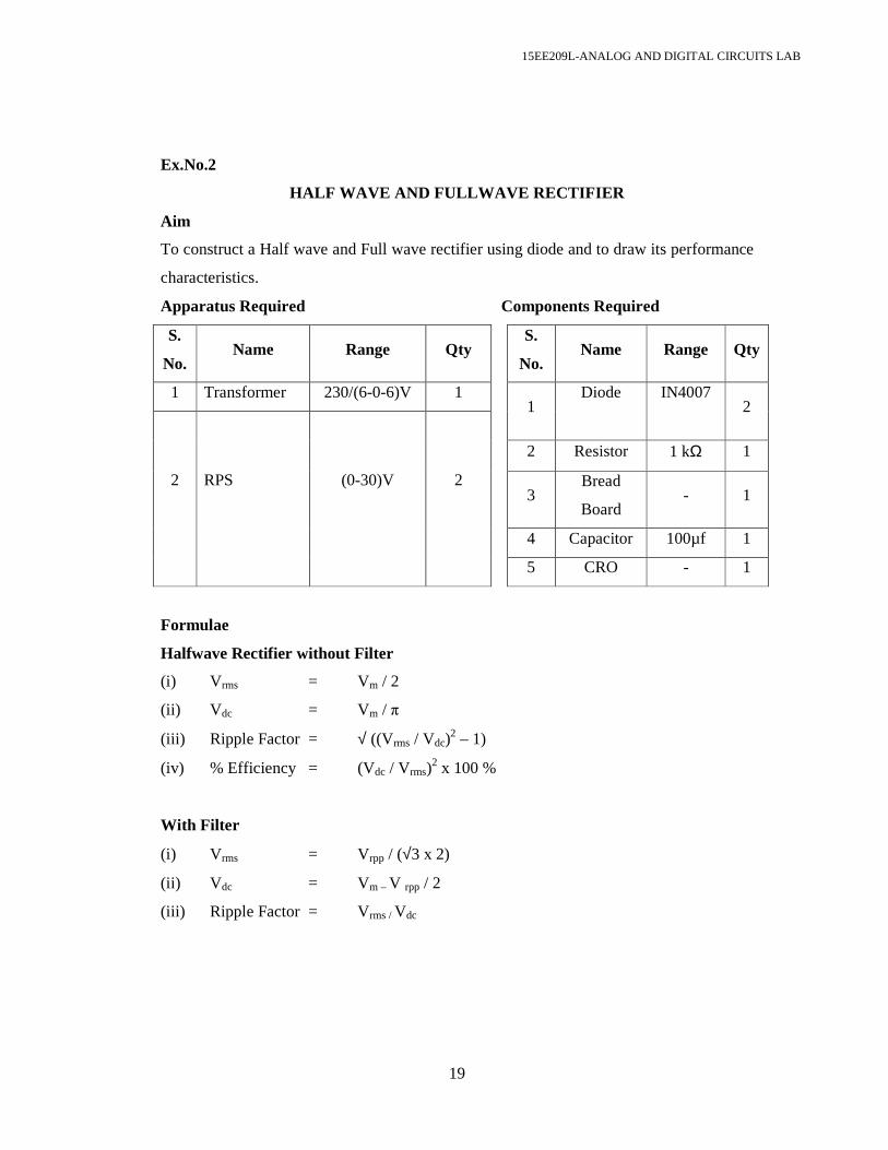
Ex.No.2
HALF WAVE AND FULLWAVE RECTIFIER
Aim
To construct a Half wave and Full wave rectifier using diode and to draw its performance
characteristics.
Apparatus Required Components Required
S.
No. Name Range Qty
S.
No. Name Range Qty
1 Transformer 230/(6-0-6)V 1 1
Diode IN4007 2
2
RPS
(0-30)V
2
2 Resistor 1 kΩ 1
3 Bread
Board - 1
4 Capacitor 100µf 1
5 CRO - 1
Formulae
Halfwave Rectifier without Filter
(i) V rms = Vm / 2
(ii) V dc = Vm / π
(iii) Ripple Factor = √ ((Vrms / Vdc)2 – 1)
(iv) % Efficiency = (Vdc / Vrms)2 x 100 %
With Filter
(i) V rms = Vrpp / (√3 x 2)
(ii) V dc = Vm – V rpp / 2
(iii) Ripple Factor = Vrms / Vdc
15EE209L-ANALOG AND DIGITAL CIRCUITS LAB
20
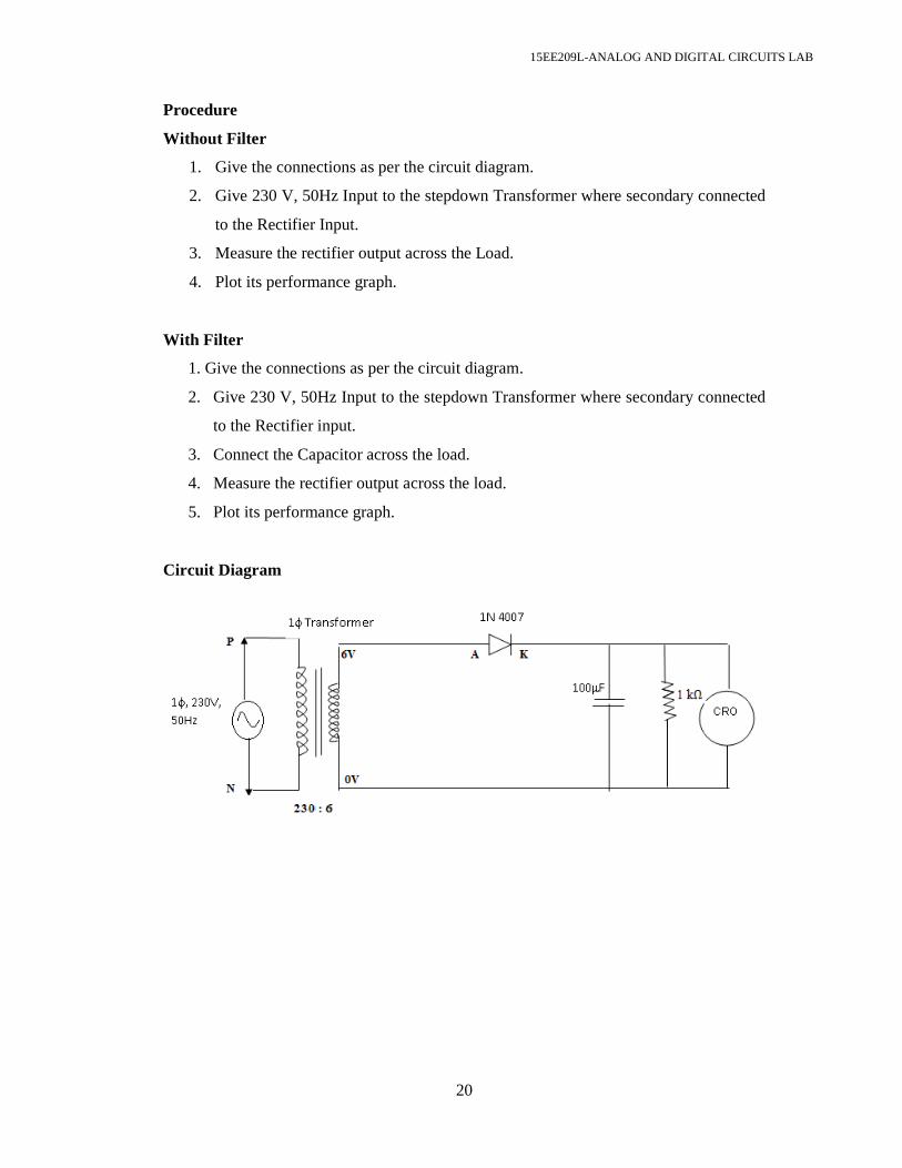
Procedure
Without Filter
1. Give the connections as per the circuit diagram.
2. Give 230 V, 50Hz Input to the stepdown Transformer where secondary connected
to the Rectifier Input.
3. Measure the rectifier output across the Load.
4. Plot its performance graph.
With Filter
1. Give the connections as per the circuit diagram.
2. Give 230 V, 50Hz Input to the stepdown Transformer where secondary connected
to the Rectifier input.
3. Connect the Capacitor across the load.
4. Measure the rectifier output across the load.
5. Plot its performance graph.
Circuit Diagram
15EE209L-ANALOG AND DIGITAL CIRCUITS LAB
21
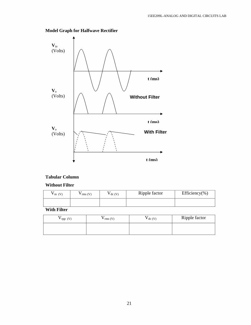
Model Graph for Halfwave Rectifier
Tabular Column
Without Filter
Vm (V) Vrms (V) Vdc (V) Ripple factor Efficiency(%)
With Filter
Vrpp (V) Vrms (V) Vdc (V) Ripple factor
V in (Volts)
t (ms)
Vo
(Volts)
t (ms)
t (ms)
Vo
(Volts)
Without Filter
With Filter
15EE209L-ANALOG AND DIGITAL CIRCUITS LAB
22
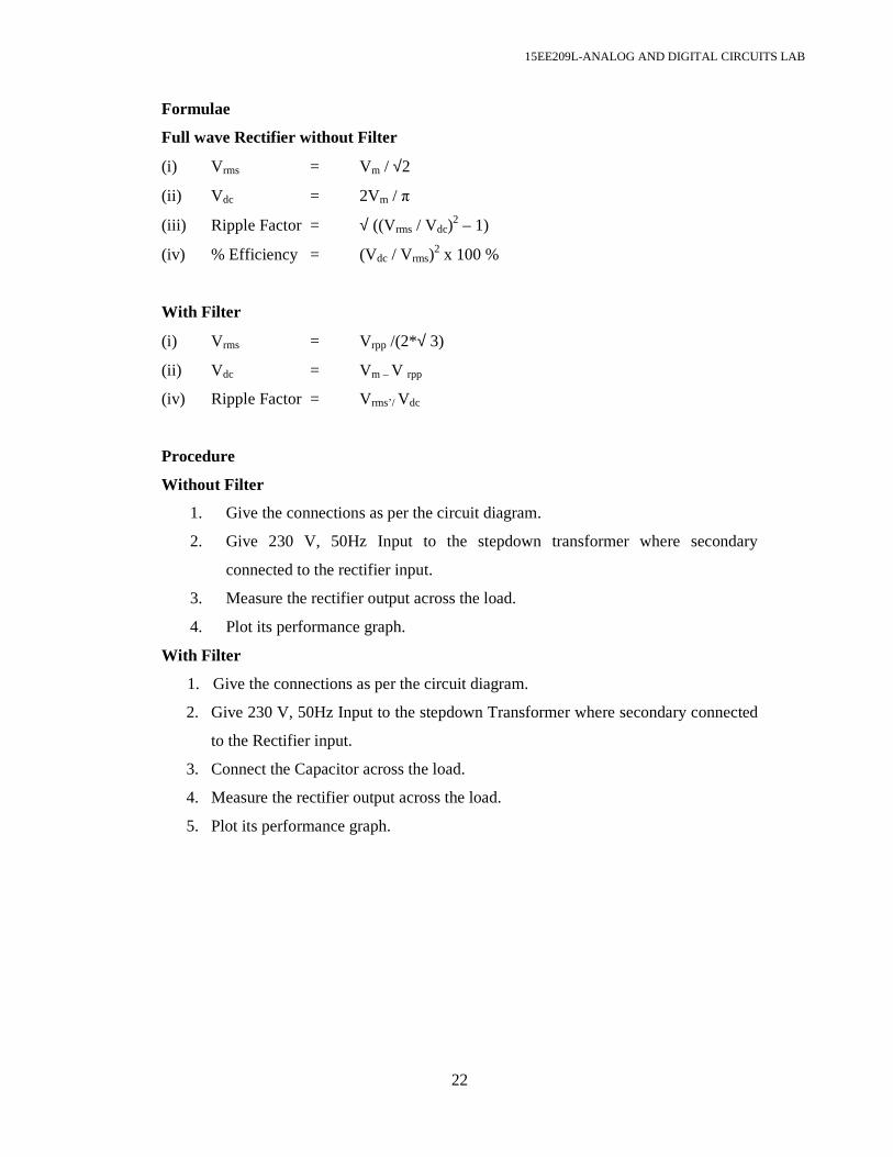
Formulae
Full wave Rectifier without Filter
(i) V rms = Vm / √2
(ii) V dc = 2Vm / π
(iii) Ripple Factor = √ ((Vrms / Vdc)2 – 1)
(iv) % Efficiency = (Vdc / Vrms)2 x 100 %
With Filter
(i) V rms = Vrpp /(2*√ 3)
(ii) V dc = Vm – V rpp
(iv) Ripple Factor = Vrms’/ Vdc
Procedure
Without Filter
1. Give the connections as per the circuit diagram.
2. Give 230 V, 50Hz Input to the stepdown transformer where secondary
connected to the rectifier input.
3. Measure the rectifier output across the load.
4. Plot its performance graph.
With Filter
1. Give the connections as per the circuit diagram.
2. Give 230 V, 50Hz Input to the stepdown Transformer where secondary connected
to the Rectifier input.
3. Connect the Capacitor across the load.
4. Measure the rectifier output across the load.
5. Plot its performance graph.
15EE209L-ANALOG AND DIGITAL CIRCUITS LAB
23
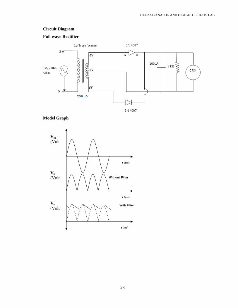
Circuit Diagram
Full wave Rectifier
Model Graph
V in (Volt
t (ms)
Vo
(Volt
t (ms)
t (ms)
Vo
(Volt
Without Filter
With Filter

15EE209L-ANALOG AND DIGITAL CIRCUITS LAB
24
Tabular Column
Without Filter
Vm Vrms Vdc Ripple factor Efficiency (%)
With Filter
Vrms Vrpp Vdc Ripple factor
Result
Thus, the performance characteristics of 1φ Half wave and Full wave rectifier
were obtained.

15EE209L-ANALOG AND DIGITAL CIRCUITS LAB
25
Post Lab Questions 1. What is TUF?
2. Mention the value of ripple factor for HWR, FWR & rectifier with centre tapped transformer.
3. What is the difference between uncontrolled rectifier and controlled rectifier?
Which is advantageous and why? 4. State the average and peak value of output voltage and current for full wave
rectifier and half wave rectifier. 5. What is PIV of a diode in half wave and full wave rectifier?

15EE209L-ANALOG AND DIGITAL CIRCUITS LAB
26
DEPT. OF ELECTRICAL & ELECTRONICS ENGINEERING SRM UNIVERSITY, Kattankulathur – 603203.
Experiment No. :3 Title of Experiment : Clippers and Clampers Name of the candidate : Register Number : Date of Experiment : Date of submission : S.No: Marks split up Maximum Marks
(50) Marks Obtained
1 Pre lab questions 5
2 Conduction 20
3 Calculation, Results and graph 20
4 Post lab questions 5
5 Total 50
Staff Signature

15EE209L-ANALOG AND DIGITAL CIRCUITS LAB
27
3.Clippers and Clampers
Pre Lab Questions 1. What are the differences between linear and nonlinear wave shaping circuit? 2. What are the applications of wave shaping circuit? 3. What is wave shaping?
4. What is the necessity of wave shaping? 5. Mention the application of clipper and clamper.
15EE209L-ANALOG AND DIGITAL CIRCUITS LAB
28
Ex. No. 3 CLIPPERS AND CLAMPERS Aim
To study the clipping and clamping circuits for different reference voltages and to verify the responses.
Apparatus Required Components Required
S.No. Name Range Qty
S.No. Name Range Qty
1 CRO 1Hz-20MHz 1
1 Resistor
Capacitor
10kΩ,
1kΩ
10µF
1
1
1
2 RPS (0–30) V 1
3 Bread
Board - 1
4 Connecting
Wires - Req
2 Diode IN4007 1
5 Function
Generator 1Hz-1MHz 1
Theory
The non-linear semiconductor diode in combination with resistor can function as
clipper circuit. Energy storage circuit components are not required in the basic process of
clipping. These circuits will select part of an arbitrary waveform which lies above or below
some particular reference voltage level and that selected part of the waveform is used for
transmission. So, they are referred as voltage limiters, current limiters, amplitude selectors
or slicers. There are three different types of clipping circuits.
1) Positive Clipping circuit.
2) Negative Clipping.
3) Positive and Negative Clipping (slicer).
In positive clipping circuit, positive cycle of Sinusoidal signal is clipped and
negative portion of sinusoidal signal is obtained in the output of reference voltage is added,
instead of complete positive cycle that portion of the positive cycle which is above the
reference voltage value is clipped. In negative clipping circuit, instead of positive portion of
sinusoidal signal, negative portion is clipped. In slicer both positive and negative portions
of the sinusoidal signal are clipped.
15EE209L-ANALOG AND DIGITAL CIRCUITS LAB
29
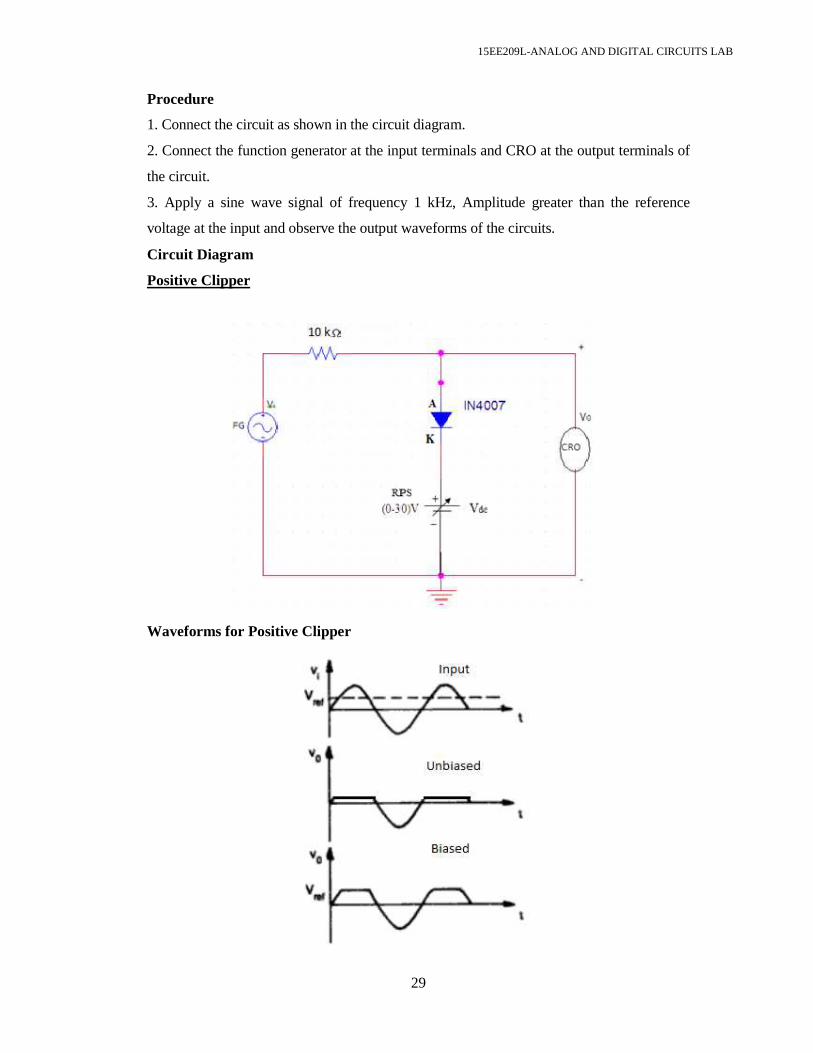
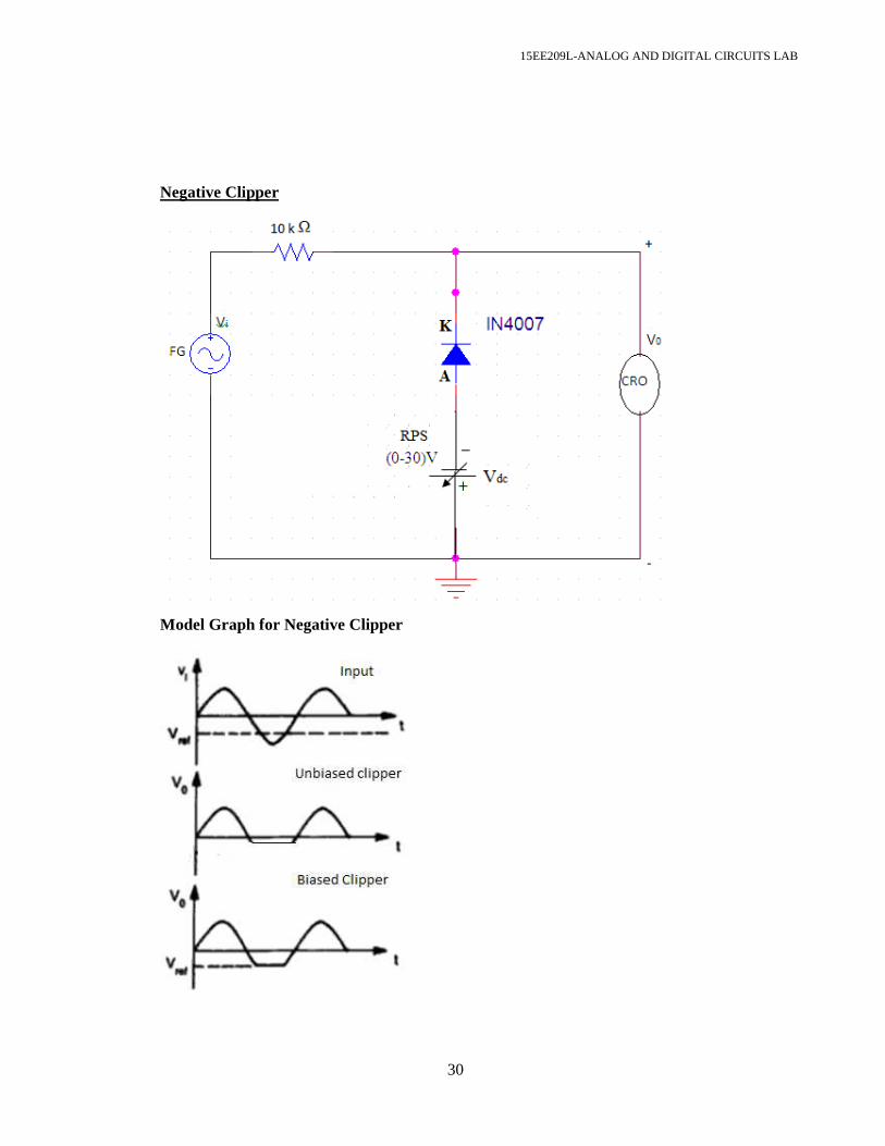
Procedure
1. Connect the circuit as shown in the circuit diagram.
2. Connect the function generator at the input terminals and CRO at the output terminals of
the circuit.
3. Apply a sine wave signal of frequency 1 kHz, Amplitude greater than the reference
voltage at the input and observe the output waveforms of the circuits.
Circuit Diagram
Positive Clipper
Waveforms for Positive Clipper
15EE209L-ANALOG AND DIGITAL CIRCUITS LAB
30
Negative Clipper
Model Graph for Negative Clipper
15EE209L-ANALOG AND DIGITAL CIRCUITS LAB
31
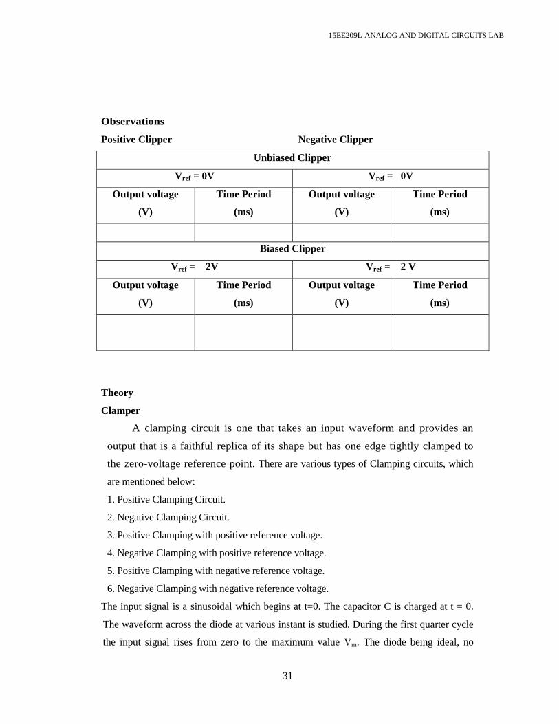
Observations
Positive Clipper Negative Clipper
Unbiased Clipper
Vref = 0V Vref = 0V
Output voltage
(V)
Time Period
(ms)
Output voltage
(V)
Time Period
(ms)
Biased Clipper
Vref = 2V Vref = 2 V
Output voltage
(V)
Time Period
(ms)
Output voltage
(V)
Time Period
(ms)
Theory
Clamper
A clamping circuit is one that takes an input waveform and provides an
output that is a faithful replica of its shape but has one edge tightly clamped to
the zero-voltage reference point. There are various types of Clamping circuits, which
are mentioned below:
1. Positive Clamping Circuit.
2. Negative Clamping Circuit.
3. Positive Clamping with positive reference voltage.
4. Negative Clamping with positive reference voltage.
5. Positive Clamping with negative reference voltage.
6. Negative Clamping with negative reference voltage.
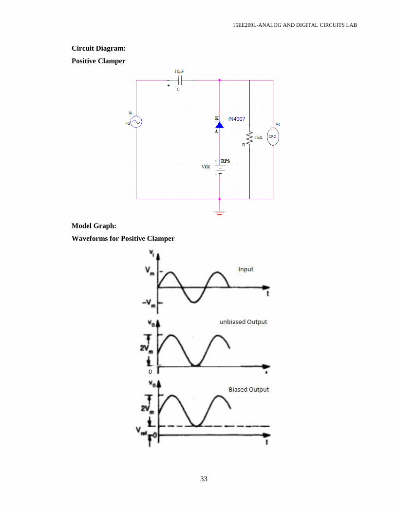
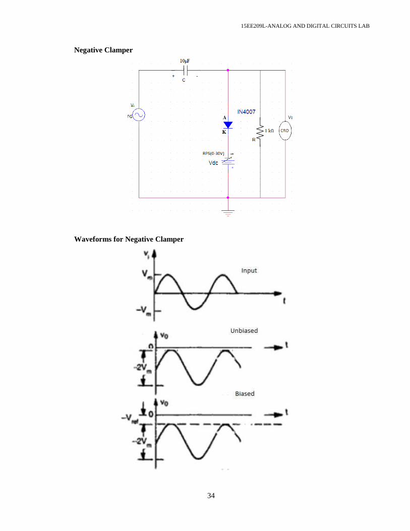
The input signal is a sinusoidal which begins at t=0. The capacitor C is charged at t = 0.
The waveform across the diode at various instant is studied. During the first quarter cycle
the input signal rises from zero to the maximum value Vm. The diode being ideal, no
15EE209L-ANALOG AND DIGITAL CIRCUITS LAB
32
forward voltage may appear across it. During this first quarter cycle the capacitor voltage
VA = Vi. The voltage across C rises sinusoidally, the capacitor is charged through the
series combination of the signal source and the diode. Throughout this first quarter cycle
the output V0 has remained zero. At the end of this quarter cycle there exists across the
capacitor a voltage VA = Vm. After the first quarter cycle, the peak has been passed and the
input signal begins to fall, the voltage VA across the capacitor is no longer able to follow the
input voltage. For in order to do so, it would be required that the capacitor discharge, and
because of the diode, such a discharge is not possible. The capacitor remains charged to the
voltage VA = Vm, and, after the first quarter cycle the output is V0 = Vi - Vm. During
succeeding cycles the positive excursion of the signal just barely reaches zero. The diode
need never again conduct, and the positive extremity of the signal has been clamped to zero.
The average value of the signal is -Vm.
Procedure
1. Connect the circuit as shown in the circuit diagram.
2. Connect the function generator at the input terminals and CRO at the output
terminals of the circuit.
3. Apply a sine wave signal of frequency 1 kHz, Amplitude greater than the reference
voltage at the input and observe the output waveforms of the circuits.
15EE209L-ANALOG AND DIGITAL CIRCUITS LAB
33
Circuit Diagram:
Positive Clamper
Model Graph:
Waveforms for Positive Clamper
15EE209L-ANALOG AND DIGITAL CIRCUITS LAB
34
Negative Clamper
Waveforms for Negative Clamper

15EE209L-ANALOG AND DIGITAL CIRCUITS LAB
35
Observations Positive Clamper Negative Clamper
Unbiased Clamper
Vref = 0V Vref = 0V
Output voltage
(V)
Time Period
(ms)
Output voltage
(V)
Time Period
(ms)
2Vm = -2Vm =
Biased Clamper
Vref = V Vref = V
Output voltage
(V)
Time Period
(ms)
Output voltage
(V)
Time Period
(ms)
2Vm+ Vref = -(2Vm+ Vref) =

15EE209L-ANALOG AND DIGITAL CIRCUITS LAB
36
Result
Thus, the clipper and clamper using diode was conducted and corresponding waveforms are obtained.
15EE209L-ANALOG AND DIGITAL CIRCUITS LAB
37
Post Lab Questions
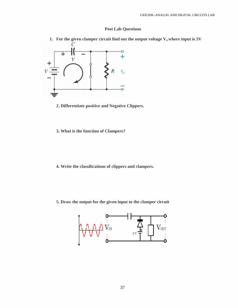
1. For the given clamper circuit find out the output voltage Vo where input is 5V
2. Differentiate positive and Negative Clippers.
3. What is the function of Clampers?
4. Write the classifications of clippers and clampers.
5. Draw the output for the given input to the clamper circuit
15EE209L-ANALOG AND DIGITAL CIRCUITS LAB
38
DEPT. OF ELECTRICAL & ELECTRONICS ENGINEERING
SRM UNIVERSITY, Kattankulathur – 603203.
Experiment No. : 4 Title of Experiment : Design of RC Phase Shift Oscillator Name of the candidate : Register Number : Date of Experiment : Date of submission : S.No: Marks split up Maximum Marks
(50) Marks Obtained
1 Pre lab questions 5
2 Conduction 20
3 Calculation, Results and graph 20
4 Post lab questions 5
5 Total 50
Staff Signature

15EE209L-ANALOG AND DIGITAL CIRCUITS LAB
39
4. Design of RC Phase Shift Oscillator Pre Lab Questions
1. What are the applications of sinusoidal oscillator and non-sinusoidal oscillators?
2. What are the factors that affect stability of an oscillators?
3. What is a phase shift oscillator?
4. What are the applications of RC phase shift oscillators?
5. Which oscillators are used to generate low frequency signals?
15EE209L-ANALOG AND DIGITAL CIRCUITS LAB
40
Ex.No. 4
DESIGN OF RC PHASE SHIFT OSCILLATOR Aim
1. To design and construct RC phase shift oscillator
2. Obtain a sinusoidal output and verify the practical frequency with calculated
theoretical frequency.
Apparatus Required
S. No. Apparatus Range Qty
1 RPS (0-30) V 1
2 CRO 1Hz-20MHz 1
3 Bread board 1 1
4 Transistor BC107 1
5 Capacitor
0.01µF 100 µF
3 1
6 Resistor
12 kΩ 68 kΩ 3.9 kΩ 1 kΩ 10 kΩ
1 1 1 1 3
7 Connecting wires
Theory
Phase Shift Oscillator
The circuit arrangement of a phase shift oscillator using NPN transistor in CE
configuration consists of voltage divider R1- R2 which provide the necessary bias, RE and
CE combinations provide temperature stability and collector resistor RC controls the
collector voltage. The oscillator output voltage is coactively coupled to the load by CC.
In case of a transistor phase shift oscillator, the output of the feedback network is
loaded appreciably by the relatively small input resistance (hie) of the transistor. Hence
instead of employing voltage series feedback, voltage shunt feedback is used for a
transistor phase shift oscillator. In this circuit, the feedback signal is coupled through the
feedback resistor R’ in series with the amplifier stage input resistance hie. The value of R’
15EE209L-ANALOG AND DIGITAL CIRCUITS LAB
41
should be such that when added with the amplifier stage input resistance hie it is equal to
R i.e., R’ + hie = R.
The circuit is set in to oscillations by any random or variation caused in the base
current, that may be due to noise inherent in the transistor or minor variation in voltage of
DC power supply. This variation in base current is amplified in collector circuit. The
output of the amplifier is supplied to an RC feedback network. The RC network produces
a phase shift of 180° between output and input voltages. Since CE amplifier produces a
phase reversal of the input signal, total phase shift becomes 360° or 0° which is essential
for regeneration or for sustained oscillations. The output of this network is same as the
originally assumed input to the amplifier and is applied to the base terminal of the
transistor. Thus, sustained variation in collector current between saturation and cutoff
values are obtained .RC phase shift network is the frequency determining network.
Design
Phase Shift Oscillator
F= 1/ (2 π RC √(6+4 (RC/R)))
R= 10 kΩ RC =3.9 kΩ F=5 kHz
5 x 10 3 = 1/ (2 π 10 x 10 3 x C x √(6+(4 x (3.9 x 10 3/ 10 x 10 3))))
C = 0.001 µ F
VCE < V CC / 2
VCE < 10 / 2
VCE = 4V
Kirchoff’s Voltage law for output circuit:
VCC - VCE = IC RC + IE RE
IC ≈ IE = 2 mA
10 – 4 - IC (RC + RE) = 0
RC + RE = 6 x 10 3 / 2
RE = 1 kΩΩΩΩ
To find R 1 and R 2:
VB = VCCR2 /(R1 + R 2) (1)
Also VB = VBE + VE
VB = 0.7 + 2 = 2.7 For Silicon Transistor VBE =0.7
From equation (1)
2.7/10 = R2 /(R1 + R 2) (2)
15EE209L-ANALOG AND DIGITAL CIRCUITS LAB
42
S= 1 + (RB / RE) (S= 20)
RB = 19 kΩ
RB = R1 R2 / (R1 + R2) (3)
Substituting (2) in (3)
19 = R1 (0.27)
R1 = 70 kΩ ≈68 kΩ R2 = 12 kΩ CE = 100 µF
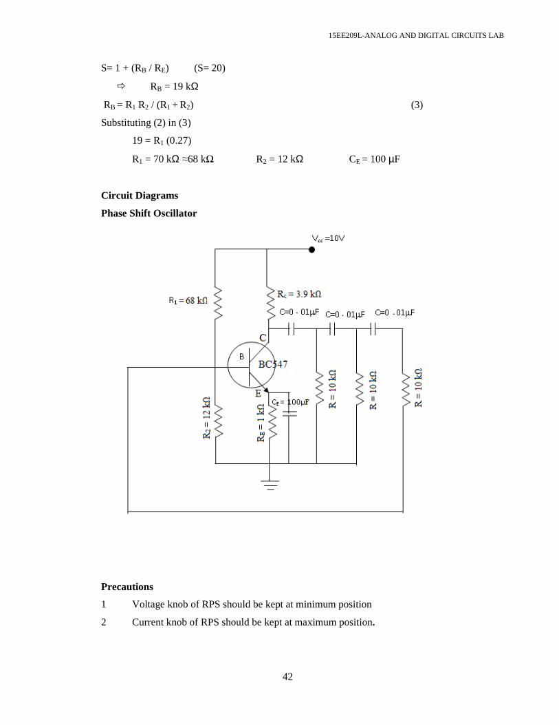
Circuit Diagrams
Phase Shift Oscillator
Precautions
1 Voltage knob of RPS should be kept at minimum position
2 Current knob of RPS should be kept at maximum position.
15EE209L-ANALOG AND DIGITAL CIRCUITS LAB
43
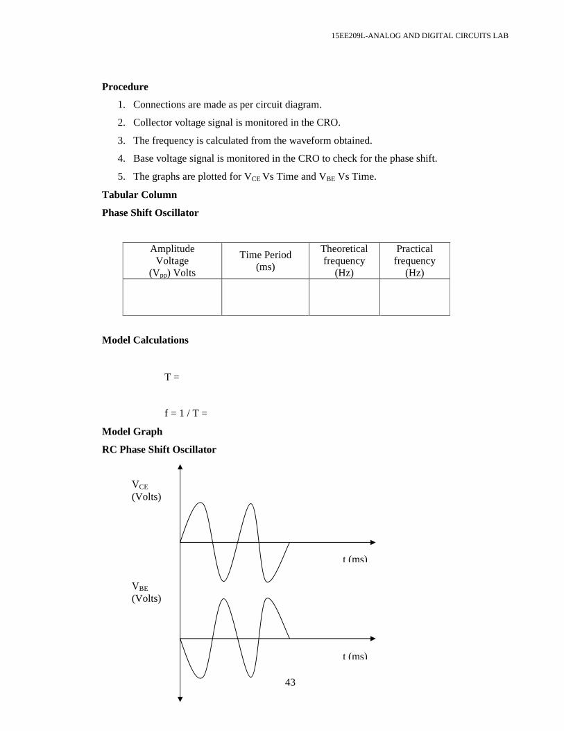
Procedure
1. Connections are made as per circuit diagram.
2. Collector voltage signal is monitored in the CRO.
3. The frequency is calculated from the waveform obtained.
4. Base voltage signal is monitored in the CRO to check for the phase shift.
5. The graphs are plotted for VCE Vs Time and VBE Vs Time.
Tabular Column
Phase Shift Oscillator
Amplitude Voltage
(Vpp) Volts
Time Period (ms)
Theoretical frequency
(Hz)
Practical frequency
(Hz)
Model Calculations
T =
f = 1 / T =
Model Graph
RC Phase Shift Oscillator
VCE (Volts)
t (ms)
VBE (Volts)
t (ms)

15EE209L-ANALOG AND DIGITAL CIRCUITS LAB
44
Result
Thus, the RC Phase shift oscillator is designed and its oscillations are
obtained.

15EE209L-ANALOG AND DIGITAL CIRCUITS LAB
45
Post Lab Questions
1. What is the basic principle of RC oscillators?
2. Why RC oscillators cannot generate high frequency oscillations?
3. Why we need a phase shift between input and output signal?
4. How is phase angle determined in RC phase shift oscillator?
5. What is the drawback of phase shift oscillators?
15EE209L-ANALOG AND DIGITAL CIRCUITS LAB
46
DEPT. OF ELECTRICAL & ELECTRONICS ENGINEERING
SRM UNIVERSITY, Kattankulathur – 603203.
Experiment No. : 5 Title of Experiment : Frequency Response of Voltage Series Feedback Amplifier Name of the candidate : Register Number : Date of Experiment : Date of submission : S.No: Marks split up Maximum Marks
(50) Marks Obtained
1 Pre lab questions 5
2 Conduction 20
3 Calculation, Results and graph 20
4 Post lab questions 5
5 Total 50
Staff Signature

15EE209L-ANALOG AND DIGITAL CIRCUITS LAB
47
5.Frequency Response of voltage Series feedback amplifier
Pre Lab Questions
1. What is the difference between voltage and current feedback?
2. How do series and shunt feedback differ from each other?
3. What is effect of negative feedback on the gain input, output impedances,
bandwidth in an amplifier?
4. What is feedback pair?
5. What happens to the frequency distortion when negative feedback is applied?
15EE209L-ANALOG AND DIGITAL CIRCUITS LAB
48
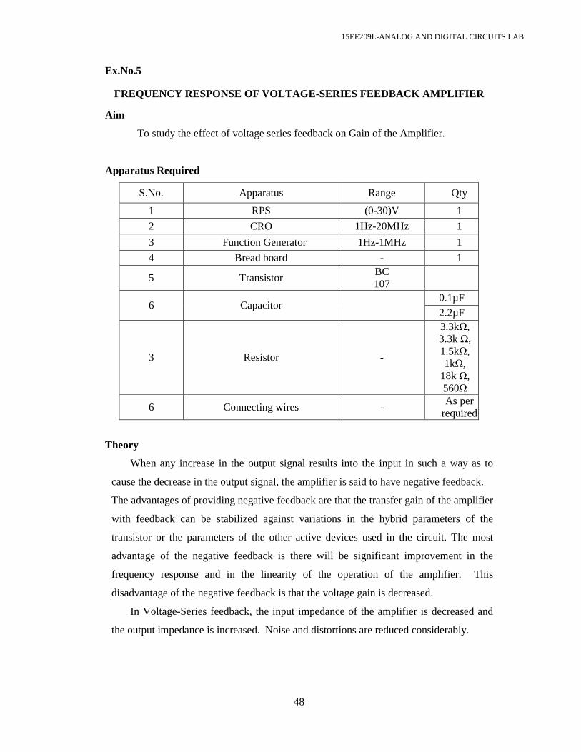
Ex.No.5
FREQUENCY RESPONSE OF VOLTAGE-SERIES FEEDBACK AMPLI FIER
Aim
To study the effect of voltage series feedback on Gain of the Amplifier.
Apparatus Required
S.No. Apparatus Range Qty
1 RPS (0-30)V 1
2 CRO 1Hz-20MHz 1
3 Function Generator 1Hz-1MHz 1
4 Bread board - 1
5 Transistor BC 107
6 Capacitor 0.1µF 2.2µF
3 Resistor -
3.3kΩ, 3.3k Ω, 1.5kΩ, 1kΩ,
18k Ω, 560Ω
6 Connecting wires - As per
required
Theory
When any increase in the output signal results into the input in such a way as to
cause the decrease in the output signal, the amplifier is said to have negative feedback.
The advantages of providing negative feedback are that the transfer gain of the amplifier
with feedback can be stabilized against variations in the hybrid parameters of the
transistor or the parameters of the other active devices used in the circuit. The most
advantage of the negative feedback is there will be significant improvement in the
frequency response and in the linearity of the operation of the amplifier. This
disadvantage of the negative feedback is that the voltage gain is decreased.
In Voltage-Series feedback, the input impedance of the amplifier is decreased and
the output impedance is increased. Noise and distortions are reduced considerably.
15EE209L-ANALOG AND DIGITAL CIRCUITS LAB
49
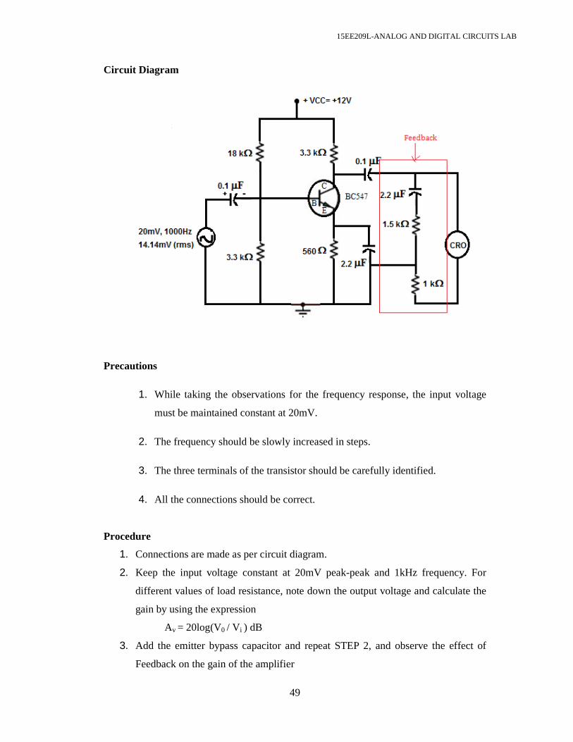
Circuit Diagram
Precautions
1. While taking the observations for the frequency response, the input voltage
must be maintained constant at 20mV.
2. The frequency should be slowly increased in steps.
3. The three terminals of the transistor should be carefully identified.
4. All the connections should be correct.
Procedure
1. Connections are made as per circuit diagram.
2. Keep the input voltage constant at 20mV peak-peak and 1kHz frequency. For
different values of load resistance, note down the output voltage and calculate the
gain by using the expression
Av = 20log(V0 / Vi ) dB
3. Add the emitter bypass capacitor and repeat STEP 2, and observe the effect of
Feedback on the gain of the amplifier
15EE209L-ANALOG AND DIGITAL CIRCUITS LAB
50
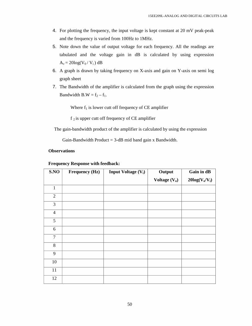
4. For plotting the frequency, the input voltage is kept constant at 20 mV peak-peak
and the frequency is varied from 100Hz to 1MHz.
5. Note down the value of output voltage for each frequency. All the readings are
tabulated and the voltage gain in dB is calculated by using expression
Av = 20log(V0 / Vi ) dB
6. A graph is drawn by taking frequency on X-axis and gain on Y-axis on semi log
graph sheet
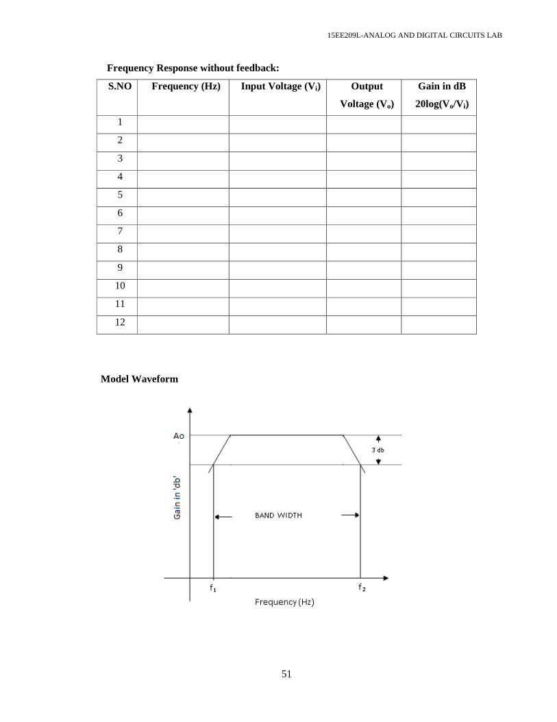
7. The Bandwidth of the amplifier is calculated from the graph using the expression
Bandwidth B.W = f2 – f1.
Where f1 is lower cutt off frequency of CE amplifier
f 2 is upper cutt off frequency of CE amplifier
The gain-bandwidth product of the amplifier is calculated by using the expression
Gain-Bandwidth Product = 3-dB mid band gain x Bandwidth.
Observations
Frequency Response with feedback:
S.NO Frequency (Hz) Input Voltage (Vi) Output
Voltage (Vo)
Gain in dB
20log(Vo/V i)
1
2
3
4
5
6
7
8
9
10
11
12
15EE209L-ANALOG AND DIGITAL CIRCUITS LAB
51
Frequency Response without feedback:
S.NO Frequency (Hz) Input Voltage (Vi) Output
Voltage (Vo)
Gain in dB
20log(Vo/V i)
1
2
3
4
5
6
7
8
9
10
11
12
Model Waveform
15EE209L-ANALOG AND DIGITAL CIRCUITS LAB
52
Result
The effect of negative feedback (Voltage -Series Feedback) on the amplifier is
observed. The voltage gain and frequency response of the amplifier are obtained. Also
gain-bandwidth product of the amplifier is calculated.

15EE209L-ANALOG AND DIGITAL CIRCUITS LAB
53
Post Lab Questions
1. What is the principle of feedback?
2. What happens to frequency distortion when negative feedback is used?
3. What is difference between current and voltage feedback?
4. How do series and shunt feedback differ from each other?
5. Why voltage series feedback is mostly used in cascade amplifier?

15EE209L-ANALOG AND DIGITAL CIRCUITS LAB
54
DEPT. OF ELECTRICAL & ELECTRONICS ENGINEERING SRM UNIVERSITY, Kattankulathur – 603203.
Experiment No. : 6 Title of Experiment : Adders, Subtractors and Flipflops Name of the candidate : Register Number : Date of Experiment : Date of submission : S.No: Marks split up Maximum Marks
(50) Marks Obtained
1 Pre lab questions 5
2 Conduction 20
3 Calculation, Results and graph 20
4 Post lab questions 5
5 Total 50
Staff Signature

15EE209L-ANALOG AND DIGITAL CIRCUITS LAB
55
6. Adders, Subtractors and Flipflops
Pre Lab Questions:
1. Derive the logical expression for full adder using K-map.
2. Derive the logical expression for half adder using K-map.
3. Derive the logical expression for half subtractor using K-map.
4. What is the difference between Latch and Flip flop?
5. How can you convert SR flip flop to JK flip flop?
15EE209L-ANALOG AND DIGITAL CIRCUITS LAB
56
EX.NO.6. ADDERS, SUBTRACTORS AND FLIP FLOPS
AIM: To construct the circuits of adder, subtractor, flipflops and verify their truth table. APPARATUS REQUIRED: S.No Name of the Apparatus Range Quantity
1. Digital IC trainer kit 1
2. Connecting wires As required
THEORY:
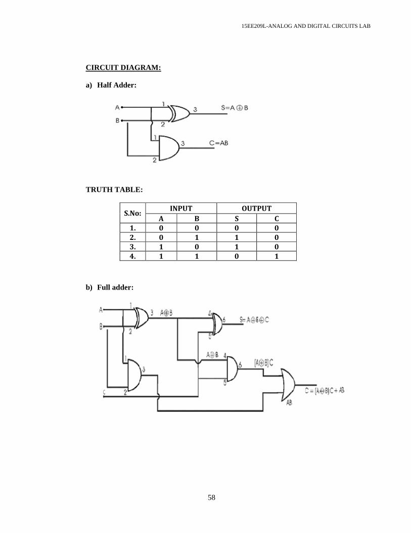
a) Half Adder:
A combinational circuit which performs the addition of two bits is called half
adder. The input variables designate the augend and the addend bit, whereas the
output variables produce the sum and carry bits.
b) Full Adder:
A combinational circuit which performs the arithmetic sum of three input bits is
called full adder. The three input bits include two significant bits and a previous
carry bit. A full adder circuit can be implemented with two half adders and one
OR gate.
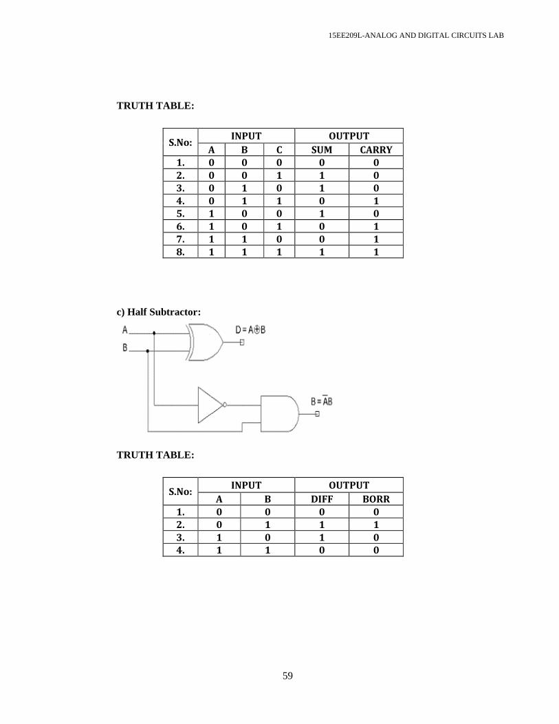
c) Half Subtractor:
A combinational circuit which performs the subtraction of two bits is called half
subtractor. The input variables designate the minuend and the subtrahend bit,
whereas the output variables produce the difference and borrow bits.
d) Full Subtractor:
A combinational circuit which performs the subtraction of three input bits is called
full subtractor. The three input bits include two significant bits and a previous
borrow bit. A full subtractor circuit can be implemented with two half subtractors
and one OR gate. THEORY: RS Flip Flop:
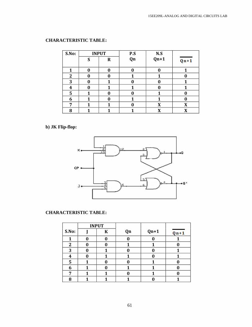
The clocked RS flip flop consists of NAND gates and the output changes its state with respect to the input on application of clock pulse. When the clock pulse is high the S and R inputs reach the second level NAND gates in their complementary form. The Flip Flop is reset when the R input is high and S input is low. The Flip Flop is set when the S input is high and R input is low. When both the inputs are high the output is in an indeterminate state.

15EE209L-ANALOG AND DIGITAL CIRCUITS LAB
57
JK Flip Flop:
The indeterminate state in the SR Flip-Flop is defined in the JK Flip Flop. JK inputs behave like S and R inputs to set and reset the Flip Flop. The output Q is ANDed with K input and the clock pulse, similarly the output Q’ is ANDed with J input and the Clock pulse. When the clock pulse is zero both the AND gates are disabled and the Q and Q’ output retain their previous values. When the clock pulse is high, the J and K inputs reach the NOR gates. When both the inputs are high the output toggles continuously. This is called Race around condition and this must be avoided.
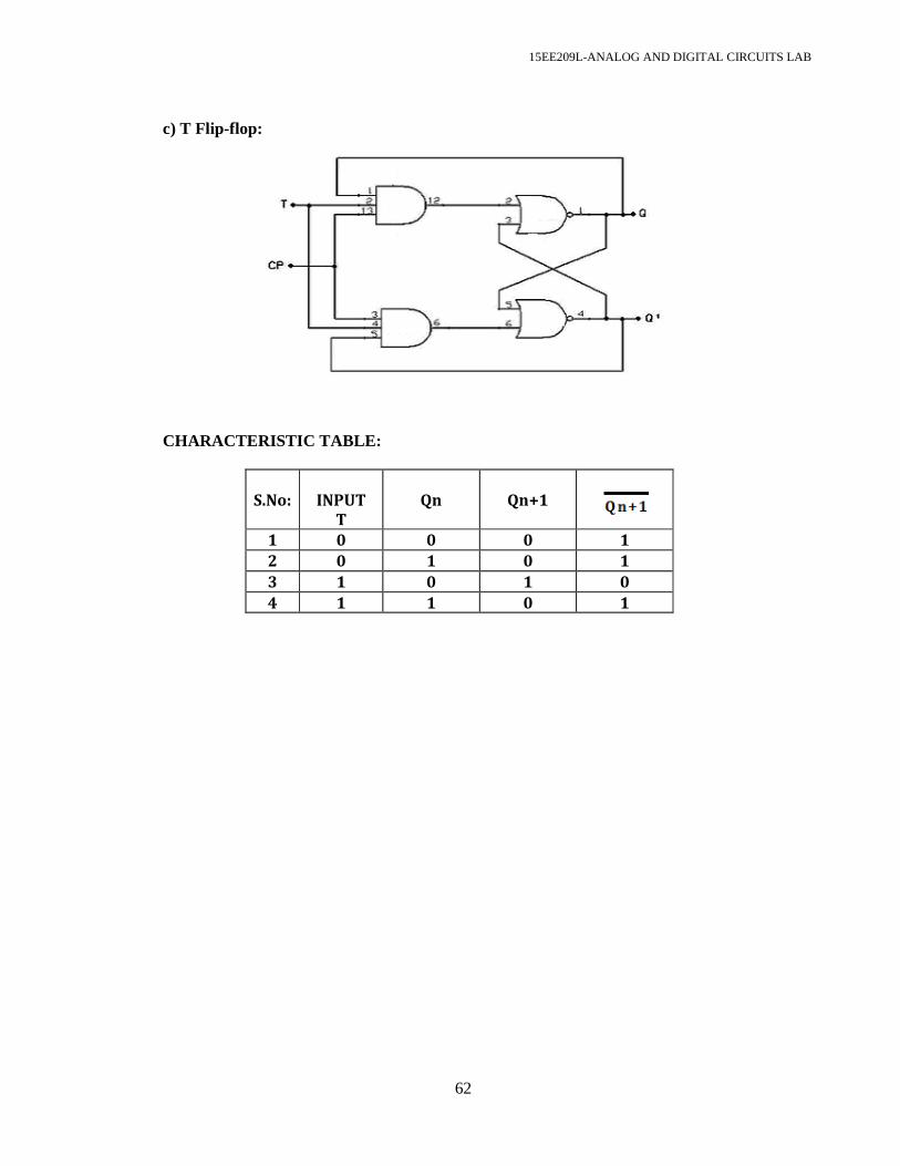
T Flip Flop: This is a modification of JK Flip Flop, obtained by connecting both inputs J and K
inputs together. T Flip Flop is also called Toggle Flip Flop. PROCEDURE: a) Half Adder:
1. Connect the circuit as per the circuit diagram 2. For various inputs, note the corresponding output. 3. Verify the truth table of half adder.
b) Full Adder:
1. Connect the circuit as per the circuit diagram. 2. For various inputs, not the corresponding output. 3. Verify the truth table of full adder.
c) Half Subtractor: 1. Connect the circuit as per the circuit diagram 2. For various inputs, note the corresponding output 3. Verify the truth table of half subtractor
d) Full Subtractor:
1. Connect the circuit as per the circuit diagram 2. For various inputs note the corresponding output 3. Verify the truth table of full subtractor
Flip-Flops:
1. Connections are given as per the circuit diagrams.
2. For all the ICs 7th pin is grounded and 14th pin is given +5 V supply.
3. Apply the inputs and observe the status of all the flip flops.
15EE209L-ANALOG AND DIGITAL CIRCUITS LAB
58
CIRCUIT DIAGRAM: a) Half Adder:
TRUTH TABLE:
S.No: INPUT OUTPUT
A B S C
1. 0 0 0 0
2. 0 1 1 0
3. 1 0 1 0
4. 1 1 0 1
b) Full adder:
15EE209L-ANALOG AND DIGITAL CIRCUITS LAB
59
TRUTH TABLE:
S.No: INPUT OUTPUT
A B C SUM CARRY
1. 0 0 0 0 0
2. 0 0 1 1 0
3. 0 1 0 1 0
4. 0 1 1 0 1
5. 1 0 0 1 0
6. 1 0 1 0 1
7. 1 1 0 0 1
8. 1 1 1 1 1
c) Half Subtractor:
TRUTH TABLE:
S.No: INPUT OUTPUT
A B DIFF BORR
1. 0 0 0 0
2. 0 1 1 1
3. 1 0 1 0
4. 1 1 0 0
15EE209L-ANALOG AND DIGITAL CIRCUITS LAB
60
d) Full Subtractor:
TRUTH TABLE:
S.No: INPUT OUTPUT
A B C DIFF BORR
1. 0 0 0 0 0
2. 0 0 1 1 1
3. 0 1 0 1 1
4. 0 1 1 0 1
5. 1 0 0 1 0
6. 1 0 1 0 0
7. 1 1 0 0 0
8. 1 1 1 1 1
CIRCUIT DIAGRAM:
a) RS Flip-flop:
15EE209L-ANALOG AND DIGITAL CIRCUITS LAB
61
CHARACTERISTIC TABLE:
S.No: INPUT P.S
Qn
N.S
Qn+1
S R
1 0 0 0 0 1
2 0 0 1 1 0
3 0 1 0 0 1
4 0 1 1 0 1
5 1 0 0 1 0
6 1 0 1 1 0
7 1 1 0 X X
8 1 1 1 X X
b) JK Flip-flop:
CHARACTERISTIC TABLE:
S.No:
INPUT
Qn
Qn+1
J K
1 0 0 0 0 1
2 0 0 1 1 0
3 0 1 0 0 1
4 0 1 1 0 1
5 1 0 0 1 0
6 1 0 1 1 0
7 1 1 0 1 0
8 1 1 1 0 1
15EE209L-ANALOG AND DIGITAL CIRCUITS LAB
62
c) T Flip-flop:
CHARACTERISTIC TABLE:
S.No:
INPUT
T
Qn
Qn+1
1 0 0 0 1
2 0 1 0 1
3 1 0 1 0
4 1 1 0 1

15EE209L-ANALOG AND DIGITAL CIRCUITS LAB
63
Result Thus, the Adders, Subtractors and flipflops were constructed and their truth tables were verified

15EE209L-ANALOG AND DIGITAL CIRCUITS LAB
64
Post Lab Questions:
1. What is half adder?
2. What is full adder?
3. What are half and full subtractor?
4. What are the characteristics of a clocked R-S flip flop? 5. Bubbled OR gate is equal to ………
15EE209L-ANALOG AND DIGITAL CIRCUITS LAB
65
DEPT. OF ELECTRICAL & ELECTRONICS ENGINEERING
SRM UNIVERSITY, Kattankulathur – 603203.
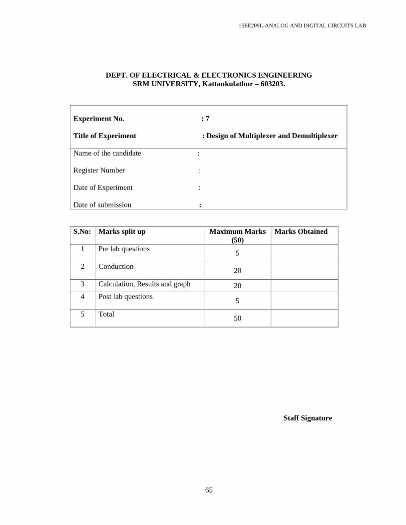
Experiment No. : 7 Title of Experiment : Design of Multiplexer and Demultiplexer Name of the candidate : Register Number : Date of Experiment : Date of submission : S.No: Marks split up Maximum Marks
(50) Marks Obtained
1 Pre lab questions 5
2 Conduction 20
3 Calculation, Results and graph 20
4 Post lab questions 5
5 Total 50
Staff Signature

15EE209L-ANALOG AND DIGITAL CIRCUITS LAB
66
7.Design of Multiplexer and Demultiplexer Pre Lab Questions: 1. What is a multiplexer? 2. What is demultiplexer? 3. Multiplexer is also called 4. Demultiplexer is also called ……. 5. What is the difference between demultiplexer and decoder?
15EE209L-ANALOG AND DIGITAL CIRCUITS LAB
67
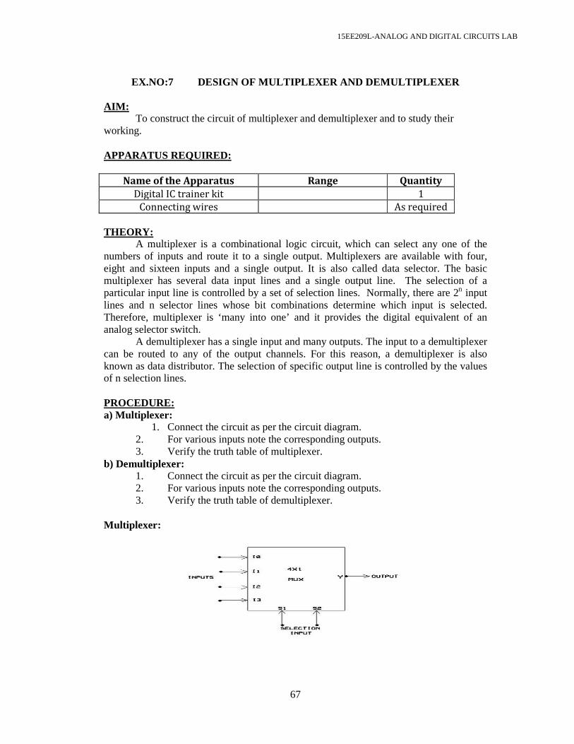
EX.NO:7 DESIGN OF MULTIPLEXER AND DEMULTIPLEXER
AIM: To construct the circuit of multiplexer and demultiplexer and to study their working. APPARATUS REQUIRED:
Name of the Apparatus Range Quantity
Digital IC trainer kit 1
Connecting wires As required
THEORY: A multiplexer is a combinational logic circuit, which can select any one of the numbers of inputs and route it to a single output. Multiplexers are available with four, eight and sixteen inputs and a single output. It is also called data selector. The basic multiplexer has several data input lines and a single output line. The selection of a particular input line is controlled by a set of selection lines. Normally, there are 2n input lines and n selector lines whose bit combinations determine which input is selected. Therefore, multiplexer is ‘many into one’ and it provides the digital equivalent of an analog selector switch. A demultiplexer has a single input and many outputs. The input to a demultiplexer can be routed to any of the output channels. For this reason, a demultiplexer is also known as data distributor. The selection of specific output line is controlled by the values of n selection lines. PROCEDURE: a) Multiplexer:
1. Connect the circuit as per the circuit diagram. 2. For various inputs note the corresponding outputs. 3. Verify the truth table of multiplexer.
b) Demultiplexer: 1. Connect the circuit as per the circuit diagram. 2. For various inputs note the corresponding outputs. 3. Verify the truth table of demultiplexer.
Multiplexer:
15EE209L-ANALOG AND DIGITAL CIRCUITS LAB
68
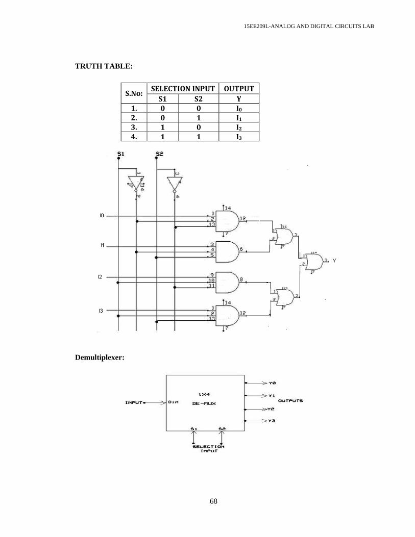
TRUTH TABLE:
S.No: SELECTION INPUT OUTPUT
S1 S2 Y
1. 0 0 I0
2. 0 1 I1
3. 1 0 I2
4. 1 1 I3
Demultiplexer:
15EE209L-ANALOG AND DIGITAL CIRCUITS LAB
69
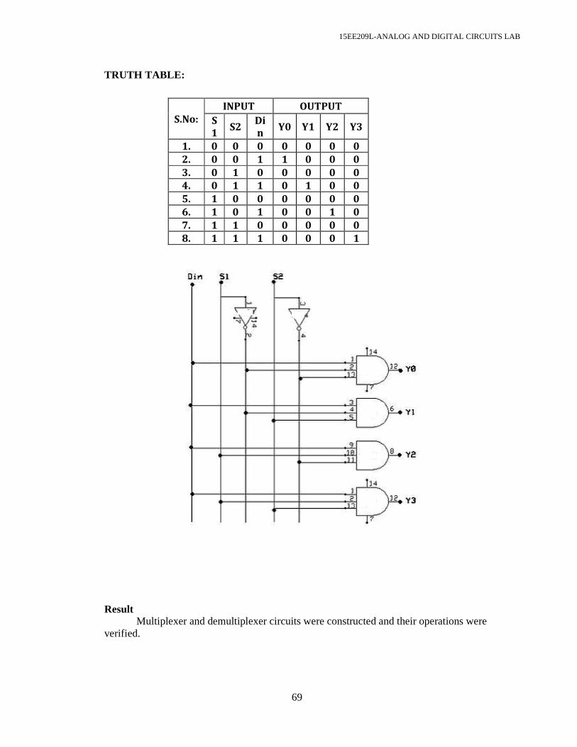
TRUTH TABLE:
S.No:
INPUT OUTPUT
S
1 S2
Di
n Y0 Y1 Y2 Y3
1. 0 0 0 0 0 0 0
2. 0 0 1 1 0 0 0
3. 0 1 0 0 0 0 0
4. 0 1 1 0 1 0 0
5. 1 0 0 0 0 0 0
6. 1 0 1 0 0 1 0
7. 1 1 0 0 0 0 0
8. 1 1 1 0 0 0 1
Result Multiplexer and demultiplexer circuits were constructed and their operations were verified.

15EE209L-ANALOG AND DIGITAL CIRCUITS LAB
70
Post Lab Questions: 1. State some applications of multiplexer and demux. 2. Build a 4:1 mux using only 2:1 mux?
3. How to implement a Master Slave flip flop using a 2 to 1 mux? `
4. How many 2 to 1 mux required to design 8 to 1 mux?
15EE209L-ANALOG AND DIGITAL CIRCUITS LAB
71
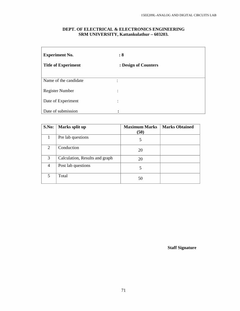
DEPT. OF ELECTRICAL & ELECTRONICS ENGINEERING SRM UNIVERSITY, Kattankulathur – 603203.
Experiment No. : 8 Title of Experiment : Design of Counters Name of the candidate : Register Number : Date of Experiment : Date of submission : S.No: Marks split up Maximum Marks
(50) Marks Obtained
1 Pre lab questions 5
2 Conduction 20
3 Calculation, Results and graph 20
4 Post lab questions 5
5 Total 50
Staff Signature

15EE209L-ANALOG AND DIGITAL CIRCUITS LAB
72
8.Design of Counters
Pre Lab Questions:
1. What are Counters and what are its types?
2. What are Ripple counters?
3. What are synchronous counters?
4. State the advantage of synchronous counter over asynchronous counters?
5. When two counters are cascaded, the overall MOD number is equal to the _________of their individual MOD numbers.
15EE209L-ANALOG AND DIGITAL CIRCUITS LAB
73
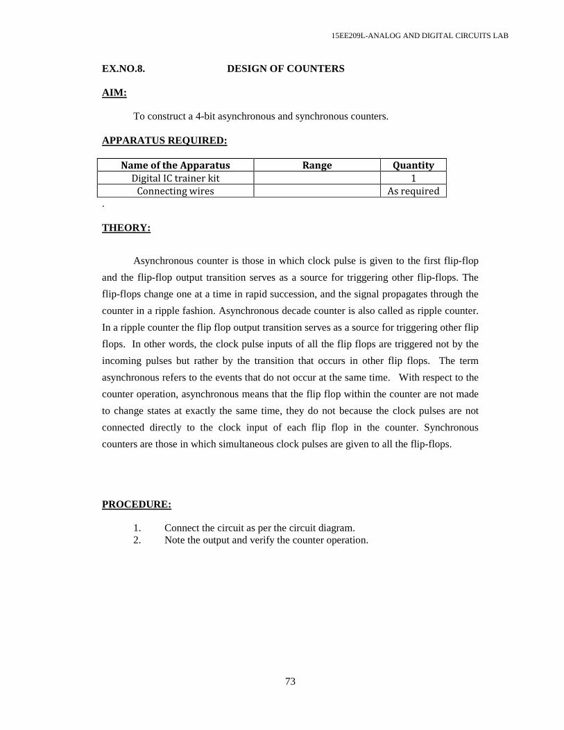
EX.NO.8. DESIGN OF COUNTERS AIM: To construct a 4-bit asynchronous and synchronous counters. APPARATUS REQUIRED:
Name of the Apparatus Range Quantity
Digital IC trainer kit 1
Connecting wires As required
. THEORY:
Asynchronous counter is those in which clock pulse is given to the first flip-flop
and the flip-flop output transition serves as a source for triggering other flip-flops. The
flip-flops change one at a time in rapid succession, and the signal propagates through the
counter in a ripple fashion. Asynchronous decade counter is also called as ripple counter.
In a ripple counter the flip flop output transition serves as a source for triggering other flip
flops. In other words, the clock pulse inputs of all the flip flops are triggered not by the
incoming pulses but rather by the transition that occurs in other flip flops. The term
asynchronous refers to the events that do not occur at the same time. With respect to the
counter operation, asynchronous means that the flip flop within the counter are not made
to change states at exactly the same time, they do not because the clock pulses are not
connected directly to the clock input of each flip flop in the counter. Synchronous
counters are those in which simultaneous clock pulses are given to all the flip-flops. PROCEDURE:
1. Connect the circuit as per the circuit diagram. 2. Note the output and verify the counter operation.
15EE209L-ANALOG AND DIGITAL CIRCUITS LAB
74
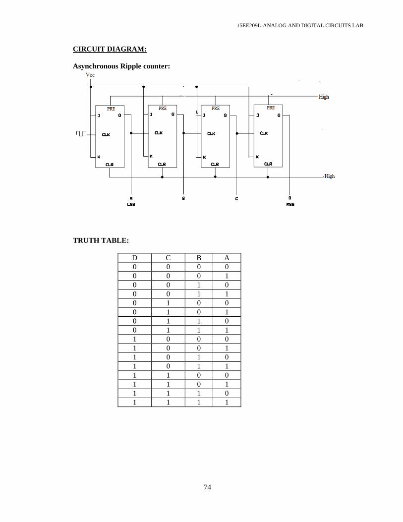
CIRCUIT DIAGRAM: Asynchronous Ripple counter:
TRUTH TABLE:
D C B A 0 0 0 0 0 0 0 1 0 0 1 0 0 0 1 1 0 1 0 0 0 1 0 1 0 1 1 0 0 1 1 1 1 0 0 0 1 0 0 1 1 0 1 0 1 0 1 1 1 1 0 0 1 1 0 1 1 1 1 0 1 1 1 1
15EE209L-ANALOG AND DIGITAL CIRCUITS LAB
75
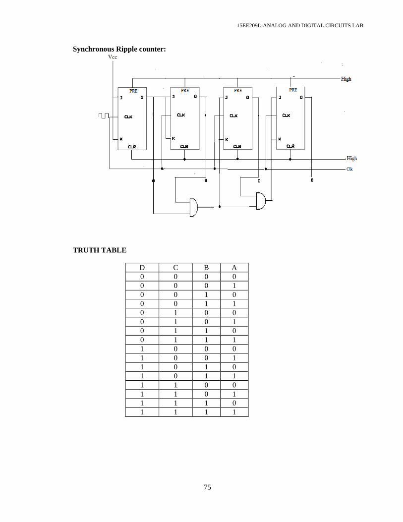
Synchronous Ripple counter:
TRUTH TABLE
D C B A 0 0 0 0 0 0 0 1 0 0 1 0 0 0 1 1 0 1 0 0 0 1 0 1 0 1 1 0 0 1 1 1 1 0 0 0 1 0 0 1 1 0 1 0 1 0 1 1 1 1 0 0 1 1 0 1 1 1 1 0 1 1 1 1

15EE209L-ANALOG AND DIGITAL CIRCUITS LAB
76
Result
Thus, the synchronous and synchronous counters were designed and truth table verified.

15EE209L-ANALOG AND DIGITAL CIRCUITS LAB
77
Post Lab Questions:
1. How many flip-flops are required to construct a decade counter?
2. What is MOD counter? 3. How many different states does a 3-bit asynchronous counter have?
4. State some applications of counters.
15EE209L-ANALOG AND DIGITAL CIRCUITS LAB
78
DEPT. OF ELECTRICAL & ELECTRONICS ENGINEERING SRM UNIVERSITY, Kattankulathur – 603203.
Experiment No. : 9 Title of Experiment : PSpice simulation of BJT and FET characteristics Name of the candidate : Register Number : Date of Experiment : Date of submission : S.No: Marks split up Maximum Marks
(50) Marks Obtained
1 Pre lab questions 5
2 Conduction 20
3 Calculation, Results and graph 20
4 Post lab questions 5
5 Total 50
Staff Signature

15EE209L-ANALOG AND DIGITAL CIRCUITS LAB
79
Pre Lab Questions:
15EE209L-ANALOG AND DIGITAL CIRCUITS LAB
80
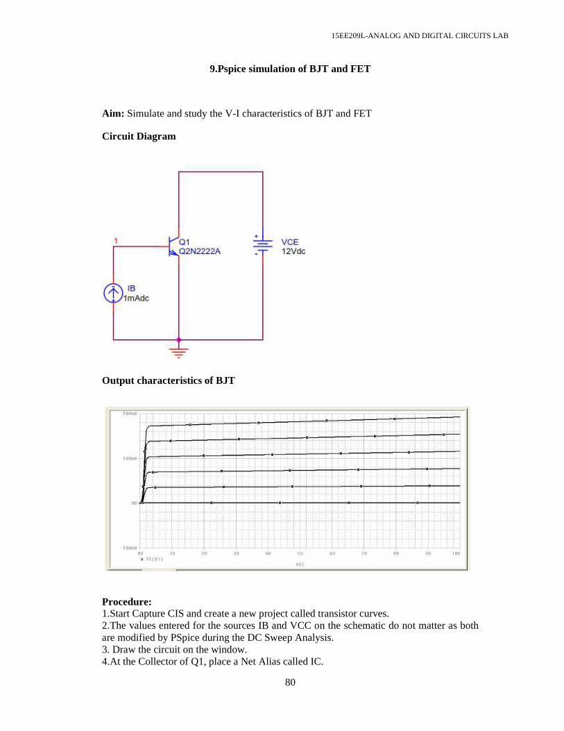
9.Pspice simulation of BJT and FET
Aim: Simulate and study the V-I characteristics of BJT and FET
Circuit Diagram
Output characteristics of BJT
Procedure: 1.Start Capture CIS and create a new project called transistor curves. 2.The values entered for the sources IB and VCC on the schematic do not matter as both are modified by PSpice during the DC Sweep Analysis. 3. Draw the circuit on the window. 4.At the Collector of Q1, place a Net Alias called IC.
15EE209L-ANALOG AND DIGITAL CIRCUITS LAB
81
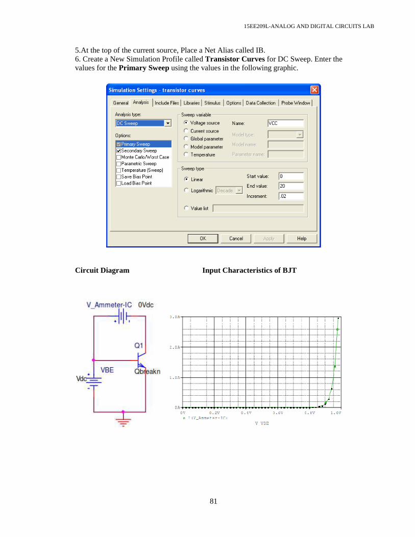
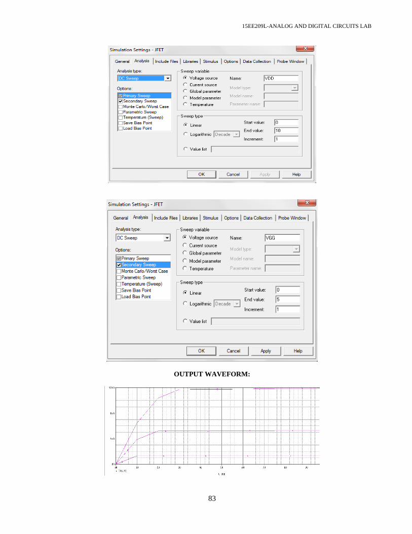
5.At the top of the current source, Place a Net Alias called IB. 6. Create a New Simulation Profile called Transistor Curves for DC Sweep. Enter the values for the Primary Sweep using the values in the following graphic.
Circuit Diagram Input Characteristics of BJT
15EE209L-ANALOG AND DIGITAL CIRCUITS LAB
82
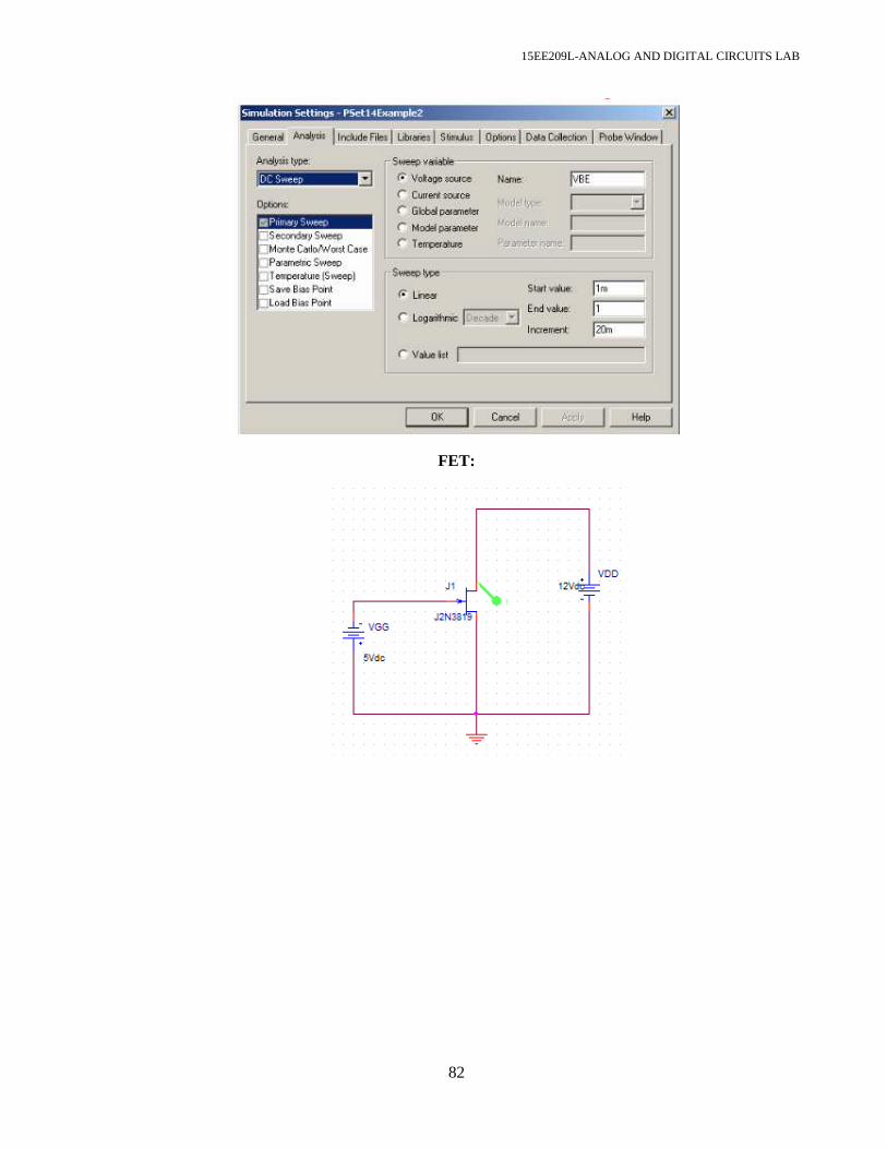
FET:
15EE209L-ANALOG AND DIGITAL CIRCUITS LAB
83
OUTPUT WAVEFORM:

15EE209L-ANALOG AND DIGITAL CIRCUITS LAB
84
Result
Thus, the simulation of BJT and FET characteristics were done using Pspice software.

15EE209L-ANALOG AND DIGITAL CIRCUITS LAB
85
Post Lab Questions:
15EE209L-ANALOG AND DIGITAL CIRCUITS LAB
86
DEPT. OF ELECTRICAL & ELECTRONICS ENGINEERING
SRM UNIVERSITY, Kattankulathur – 603203.
Experiment No. :10 Title of Experiment : Simulation of Digital Logic Circuits using VHDL Name of the candidate : Register Number : Date of Experiment : Date of submission : S.No: Marks split up Maximum Marks
(50) Marks Obtained
1 Pre lab questions 5
2 Conduction 20
3 Calculation, Results and graph 20
4 Post lab questions 5
5 Total 50
Staff Signature

15EE209L-ANALOG AND DIGITAL CIRCUITS LAB
87
Pre Lab Questions:
15EE209L-ANALOG AND DIGITAL CIRCUITS LAB
88
EX.NO:10 SIMULATION OF DIGITAL LOGIC CIRCUITS USIN G VHDL AIM: To design and simulate the digital logic circuits using Xilinx Software. SOFTWARE REQUIRED: XILINX software and FPGA Trainer Kit VHDL CODE: AND GATE library IEEE; use IEEE.STD_LOGIC_1164.ALL; use IEEE.STD_LOGIC_ARITH.ALL; use IEEE.STD_LOGIC_UNSIGNED.ALL; entity and1 is Port ( a : in STD_LOGIC; b : in STD_LOGIC; c : out STD_LOGIC); end and1; architecture data_flow of and1 is begin c<=a and b; end data_flow; #PACE: Start of PACE I/O Pin Assignments NET "a" LOC = "p106" ; NET "b" LOC = "p107" ; NET "c" LOC = "p179" ;
NOR GATE library IEEE; use IEEE.STD_LOGIC_1164.ALL; use IEEE.STD_LOGIC_ARITH.ALL; use IEEE.STD_LOGIC_UNSIGNED.ALL; entity nor1 is Port ( a : in STD_LOGIC; b : in STD_LOGIC; c : out STD_LOGIC); end nor1; architecture data_flow of nor1 is begin c<=a nor b; end data_flow; #PACE: Start of PACE I/O Pin Assignments NET "a" LOC = "p106" ; NET "b" LOC = "p107" ; NET "c" LOC = "p179" ;
15EE209L-ANALOG AND DIGITAL CIRCUITS LAB
89
OR GATE library IEEE; use IEEE.STD_LOGIC_1164.ALL; use IEEE.STD_LOGIC_ARITH.ALL; use IEEE.STD_LOGIC_UNSIGNED.ALL; entity or2 is Port ( a : in STD_LOGIC; b : in STD_LOGIC; c : out STD_LOGIC); end or2; architecture data_flow of or2 is begin c<=a or b; end data_flow; #PACE: Start of PACE I/O Pin Assignments NET "a" LOC = "p106" ; NET "b" LOC = "p107" ; NET "c" LOC = "p179" ;
XOR library IEEE; use IEEE.STD_LOGIC_1164.ALL; use IEEE.STD_LOGIC_ARITH.ALL; use IEEE.STD_LOGIC_UNSIGNED.ALL; entity xor1 is Port ( a : in STD_LOGIC; b : in STD_LOGIC; c : out STD_LOGIC); end xor1; architecture data_flow of xor1 is begin c<=a xor b; end data_flow; #PACE: Start of PACE I/O Pin Assignments NET "a" LOC = "p106" ; NET "b" LOC = "p107" ; NET "c" LOC = "p179" ;
FULL ADDER library IEEE; use IEEE.std_logic_1164.all; entity fa is port (a : in std_logic; b : in std_logic; cin : in std_logic; sum : out std_logic; cout : out std_logic); end fa; -- description of fa using concurrent signal assignments architecture rtl of fa is begin sum <= (a xor b) xor cin;
15EE209L-ANALOG AND DIGITAL CIRCUITS LAB
90
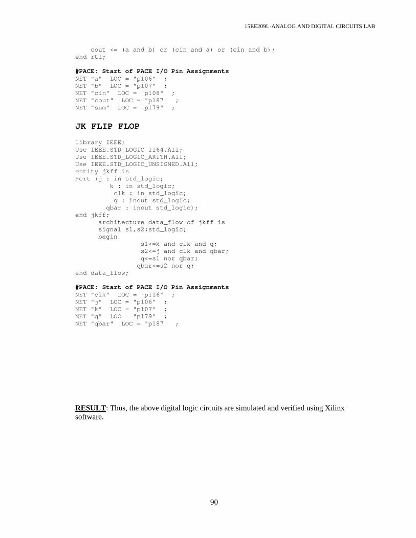
cout <= (a and b) or (cin and a) or (cin and b); end rtl; #PACE: Start of PACE I/O Pin Assignments NET "a" LOC = "p106" ; NET "b" LOC = "p107" ; NET "cin" LOC = "p108" ; NET "cout" LOC = "p187" ; NET "sum" LOC = "p179" ;
JK FLIP FLOP library IEEE; Use IEEE.STD_LOGIC_1164.All; Use IEEE.STD_LOGIC_ARITH.All; Use IEEE.STD_LOGIC_UNSIGNED.All; entity jkff is Port (j : in std_logic; k : in std_logic; clk : in std_logic; q : inout std_logic; qbar : inout std_logic); end jkff; architecture data_flow of jkff is signal s1,s2:std_logic; begin s1<=k and clk and q; s2<=j and clk and qbar; q<=s1 nor qbar; qbar<=s2 nor q; end data_flow; #PACE: Start of PACE I/O Pin Assignments NET "clk" LOC = "p116" ; NET "j" LOC = "p106" ; NET "k" LOC = "p107" ; NET "q" LOC = "p179" ; NET "qbar" LOC = "p187" ;
RESULT: Thus, the above digital logic circuits are simulated and verified using Xilinx software.

15EE209L-ANALOG AND DIGITAL CIRCUITS LAB
91
Post Lab Questions:
Recommended