DATA SHEET
1
STP2202ABGA
DSC
Dual Processor System Controller
D
ESCRIPTION
The STP2202BGA is the Dual Processor System Controller, also referred to as DSC, used in a low-cost high-performing two-processor system. DSC’s primary functions are to provide data coherence control, memory control, datapaths control, flow control, transaction ordering, and address routing. It regulates the flow of requests and data on the system’s “UPA” interconnect based on dual cache coherent tags for each of the two processors.
F
EATURES
• Performs as a centralized system controller.• Implements four ports on two UPA buses; two for the processors, one for the UPA to SBus interface (U2S)
and one for the Fast Frame Buffer (FFB).• Can also be configured with just one processor.• Schedules the crossbar switch and controls the flow on the UPA data buses.• It can support up to sixteen 60ns SPARCstation
20 type DRAM SIMMs, each with capacities of 16MB, 32MB, 64MB, or 128MB. This can support a total 2GB of system memory.
• Coordinates interrupt and reset inputs from Reset, Interrupt and Clock (RIC) and distributes them to the other system components.
• Provides an 8-bit EBus interface to allow read/write of the DSC’s internal registers.• Operates at a maximum frequency of 100 MHz (10 ns cycle time).• Includes a JTAG interface for full chip scan during system tests.• Contains a Phase-Locked-Loop (PLL) to remove skew introduced by the internal clock distribution
network.
June 1998
2
STP2202ABGA
Dual Processor System Controller DSC
June 1998
Sun Microsystems, Inc
R
ELATED
P
RODUCTS
F
UNCTIONAL
D
ESCRIPTION
System
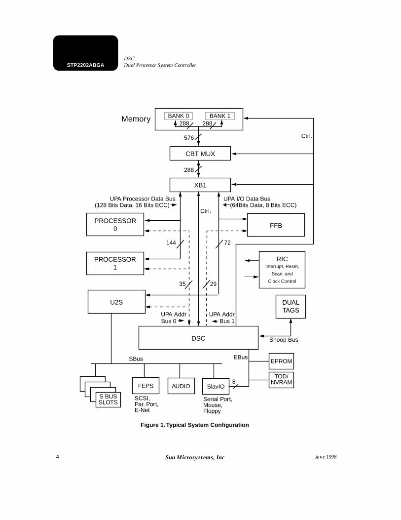
The system units (see Typical System Configuration) typically interface with the DSC as follows:
UltraSPARC Modules (STP5110)
The processors are essentially isolated from the rest of the system except system memory, and communicate with the DSC through their ports on UPA Address Bus 0. The major functions the DSC provides for the pro-cessors are Port control, System Memory Path control, and issuance of necessary resets. Using the Snoop Bus, the DSC monitors a duplicate set of the UPA Address Bus 0 Port tags, and maintains order during coherent operations.
U2S (STP2220)
The U2S interfaces with the DSC through the I/O Data Bus and the UPA Address Bus 1. It is treated just like another client, and has no other special communication with the DSC.
FEPS (STP2002)
FEPS is Fast Ethernet Parallel port SCSI. It provides the following I/O devices: 10/100 Mb/sec Ethernet, 20 Mb/sec Fast SCSI and a standard parallel port.
SlavIO (STP2001)
SlavIO provides most of the SUNness I/O requirements. It contains serial ports, floppy, keyboard/mouse and EBus control. Since the DSC contains no data path, the 8-bit EBus, controlled by the SlavIO chip, is used by the processor(s) to read/write internal registers of the DSC.
Name Description STP Part No.
APC Audio Controller STP2024QFP
CPU Module UltraSPARC Module STP5110
DTAG Dual Tag Synchronous SRAM N/A
Ecache 2nd Level High Speed Data and Tag Cache N/A
FEPS High Performance Master System I/O Controller STP2002QFP
RIC Reset/Interrupt/Clock Controller STP2210QFP
SlavIO Slave System I/O Controller STP2001QFP
UDB UltraSPARC-I Data Buffer STP1080BGA
UltraSPARC-I High Performance 64-Bit RISC Processor STP1030BGA
U2S UPA-to-SBus Interface STP2220BGA
XB1 Crossbar Switch STP2230SOP
3
Dual Processor System ControllerDSC
STP2202ABGA
June 1998
Sun Microsystems, Inc
XB1 (STP2230SOP)
The three port crossbar interconnects a 144-bit (128 + 16 ECC) UPA data bus accessed by two processors, a 72-bit (64 + 8 ECC) UPA data bus accessed by the U2S and the FFB, and a 288-bit wide memory bus. There is a 2 port switch (CBT) between 288-bit memory bus and 576-bit SIMM data. The crossbar and system memory access are controlled by the DSC.
Cross Bar Technology Sus Switch (CBT)
The CBT switch is a 2 port switch between a 576 bit memory bus (SIMM side) and a 288 bit data bus (XB1 side). To maintain a manageable pin count, the devices are sliced so that 18 parts are needed to form the com-plete switch function. The CBT switch part number is: TI SN74CBT16233.
Fast Frame Buffer (FFB)
On-board graphics interfaces with the system through an output only UPA64S graphics port. The FFB is always the slave, with the DSC the master. UPA Address Bus 1 is used to supply address information, The UPA I/O Data Bus is the output path for the graphics data.
RIC (STP2210)
The RIC’s main function for the DSC is the import of reset status from system power on, pushbutton, or keyboard resets.
DTAG
Dual Tag SRAM attached to DSC’s coherency controller, which keeps a copy of each processor’s tags.
Note:
The U2P and UIO could replace the U2S and SlavIO, respectively, if the system utilizes PCI buses.
4
STP2202ABGA
Dual Processor System Controller DSC
June 1998
Sun Microsystems, Inc
Figure 1. Typical System Configuration
Memory
XB1
FFB
DSC
DUALTAGS
PROCESSOR0
PROCESSOR1
U2S
BANK 0 BANK 1
EPROM
TOD/NVRAM
S BUSSLOTS
FEPS AUDIO SlavIO
UPA AddrBus 1
UPA AddrBus 0
SCSI,Par. Port,E-Net
Serial Port,Mouse,Floppy
UPA I/O Data BusUPA Processor Data Bus
Snoop Bus
EBusSBus
Ctrl.
Ctrl.
288
288
(128 Bits Data, 16 Bits ECC) (64Bits Data, 8 Bits ECC)
35 29
144 72
8
RICInterrupt, Reset,
Scan, and
Clock Control
CBT MUX
576
288
5
Dual Processor System ControllerDSC
STP2202ABGA
June 1998
Sun Microsystems, Inc
MemAddr1[12:0]
RAS_L[3:0]CAS_L[7:0]
WE_L[3:0]
MRBCtrl0,1
MWBCtrl0,1
XB1Cmd0,1[3:0]
SReply0[4:0]
SReply1[4:0]
SReply2[4:0]
AddrBus0[34:0]
AddrPar0
AddrVal0[3:0]
SCReq0
ReqIn0[2:0]
ECCValid0
ECCValid1
DataStall0
DataStall1
AddrBus1[28:0]AddrVal1
PReply0[4:0]
PReply1[4:0]
PReply3[1:0]
SysRst_L
X_Reset_L
P_Reset_L
UPA_Reset0_L
UPA_Reset1_L
UPA_XIR_L
EB_CS_L
EB_WR_L
DEBUG[3:0]
EB_ADDR[2:0]
EB_DATA[7:0]
JTAG_TCK
JTAG_TMS
JTAG_TDO
JTAG_TDI
CLK+
CLK-
PORTINTERFACE
DATAPATH
MEMCONTROL
EBUSINTERFACE
JTAG
CLOCK/
EB_RD_L
JTAG_TRST_L
PLL_BYPASS
PReply2[4:0]
PLL_GND
PLL_VCC
5V_REF
MemAddr0[12:0]
SReply3[2:0]
Bank_Sel[3:0]
Snp_Index[15:0]
SnpWE_L
SnpOE_LSnp_Tag[11:0]Snp_State[1:0]
Snp_Par
MISCPLL/
COHERENCYCONTROL
SCHEDULE
Snp_Clk
PM_OUT
DTA
G In
terf
ace
(PIF)
(EB)
(CC)
(MC)
(DPS)
Figure 2. DSC Block Diagram
6
STP2202ABGA
Dual Processor System Controller DSC
June 1998
Sun Microsystems, Inc
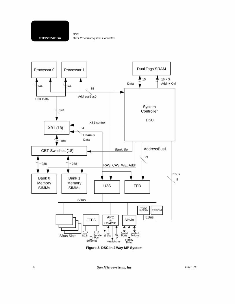
Figure 3. DSC in 2 Way MP System
SBus Slots
FEPS
SCSI
Ethernet
ParallelPort
APC&
CS4231
Linein out Mic
In
SBus
Headphone
SerialPorts
KeybrdMouse
Slavio
TOD/NVRAM
FloppyDrive
EBus
EPROM
Processor 0 Processor 1
MemorySIMMs
MemorySIMMs
CBT Switches (18)
288288
288
XB1 (18)
144
144
144
UPA Data
U2S
64
UPA64SData
FFB
35
AddressBus0
System Controller
DSC
Dual Tags SRAM
29
AddressBus1
EBus
8
XB1 control
Bank Sel
RAS, CAS, WE, Addr
Bank 0 Bank 1
Data15 16 + 3
Addr + Ctrl
7
Dual Processor System ControllerDSC
STP2202ABGA
June 1998
Sun Microsystems, Inc
F
UNCTIONAL
B
LOCKS
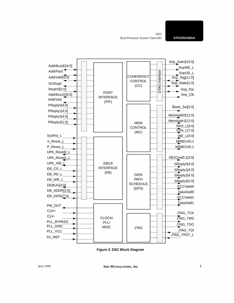
DSC is divided into five major blocks:
1. Port Interface (PIF)
2. Datapath Scheduler (DPS)
3. Memory Controller (MC)
4. Coherency Controller(CC)
5. EBus Interface (EB)
Their functions are described in further detail in the following sections.
Port Interface (PIF)
The PIF supports two UPA busses. It is responsible for receiving packets, decoding their destinations, and for-warding packets to the proper destinations. Cached transactions are typically forwarded to the Memory Controller. Non-cached transactions are typically forwarded to the proper slave.
UPA address bus 0 has three UPA ports. Each Processor and the U2S can act as either a UPA master or a slave.
UPA address bus 1 implements the UPA64S subset only. It supports only a single graphics slave. This bus is output only, not bidirectional, and DSC is always the master of this bus. In addition, the graphics slave will only generate and receive truncated PReply and SReply signals.
PIF controls the arbitration on UPA address bus 0. There are three other masters on this bus, the two proces-sors and U2S. PIF uses a distributed round robin algorithm as described in the “UPA Interconnect Architecture” document.
PIF also receives all PReplys from UPA clients.
PIF contains four sets of the following registers (one for each UPA port):
1. SC_Port_Config registers.
2. SC_Port_Status registers.
These registers are described in further detail in the “DSC User’s Manual” document. Part No. 950-2117-01
Datapath Scheduler (DPS)
The DPS is responsible for regulating the flow of data throughout the system. It generates the following:
1. BMX commands for XB1 crossbar switch.
2. S_REPLYs for all clients.
3. UPA_DATASTALL signals.
4. UPA_ECCVALID signals.
DPS contains no software visible registers.
Memory Controller (MC)
MC is responsible for controlling the SIMMs. It performs the following functions.
8
STP2202ABGA
Dual Processor System Controller DSC
June 1998
Sun Microsystems, Inc
1. Generates timing for read, write, and refresh.
2. Converts the physical address in the UPA packet into row and column addresses.
3. Maintains refresh timer.
4. Controls loading and unloading of data from the XB1 read and write buffers.
5. Controls the memory switch CBT (FET multiplexer) selects.
PIF forwards memory requests to the MC. MC communicates with the DPS to schedule delivery of data.
The operation of MC and the memory subsystem is described in further detail in the “DSC User’s Manual” document, Part No. 950-2117-01.
Coherency Controller (CC)
The CC is responsible for maintaining cache coherency at the system level. A copy of each processors tags is kept in “Dual Tag” RAM that is connected to the CC. The CC checks the Dual tags or “snoops” on all of the cacheable transactions. From this snoop it can determine the appropriate response. The operation of the Coherency Controller is further described in the “DSC User’s Manual” document.
EBus Interface (EB)
EB implements an interface to EBus, an asynchronous 8-bit interface controlled by Slavio. Since DSC contains no data path, all reading and writing of internal registers has to take place via EBus. Since all internal registers are 32 bits wide, EB has to perform packing and unpacking.
EB is the only block which can be used in both USC and DSC with minimal change.
The EB block implements reset logic.
The EB block contains a number of global registers.
1. SC_Control register for controlling resets and logging reset status.
2. SC_ID register, which contains DSC’s JEDEC ID number, implementation and version numbers, and the number of UPA ports that this chip supports.
3. Performance counters: SC_Perf_Ctrl, SC_Perf1, and SC_Perf2. These counters can be configured to count various events for performance analysis.
The global registers are described in further detail in the “DSC User’s Manual” document.
The operation of EB is described in further detail in the “DSC User’s Manual” document.
Performance Monitors
The DSC has a small block that contains logic to monitor performance. Performance registers can be read after being set up by programming the SC_Perf_Ctrl register. These registers are defined in the “DSC User’s Man-ual”. These registers are accessed through the EBus.
JTAG Interface
The DSC has a JTAG interface. This interface block is common to the system ASICs and ports the signal set used for debugging purposes.
9
Dual Processor System ControllerDSC
STP2202ABGA
June 1998
Sun Microsystems, Inc
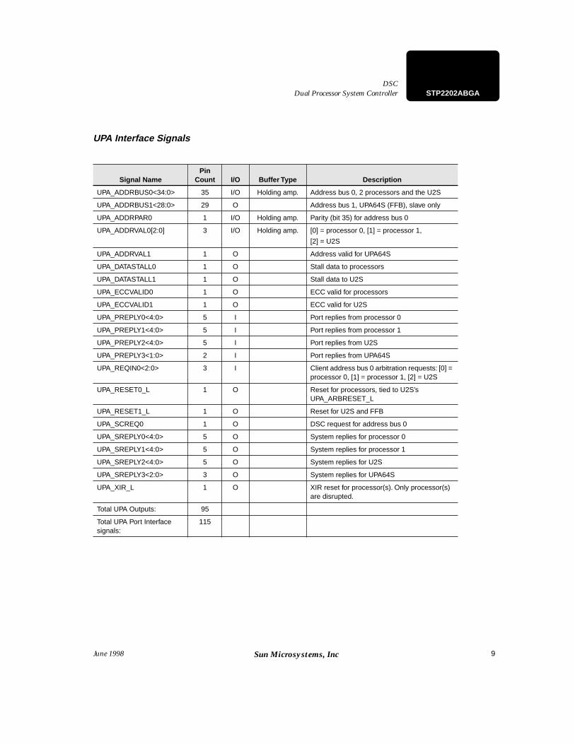
UPA Interface Signals
Signal NamePin
Count I/O Buffer Type Description
UPA_ADDRBUS0<34:0> 35 I/O Holding amp. Address bus 0, 2 processors and the U2S
UPA_ADDRBUS1<28:0> 29 O Address bus 1, UPA64S (FFB), slave only
UPA_ADDRPAR0 1 I/O Holding amp. Parity (bit 35) for address bus 0
UPA_ADDRVAL0[2:0] 3 I/O Holding amp. [0] = processor 0, [1] = processor 1,
[2] = U2S
UPA_ADDRVAL1 1 O Address valid for UPA64S
UPA_DATASTALL0 1 O Stall data to processors
UPA_DATASTALL1 1 O Stall data to U2S
UPA_ECCVALID0 1 O ECC valid for processors
UPA_ECCVALID1 1 O ECC valid for U2S
UPA_PREPLY0<4:0> 5 I Port replies from processor 0
UPA_PREPLY1<4:0> 5 I Port replies from processor 1
UPA_PREPLY2<4:0> 5 I Port replies from U2S
UPA_PREPLY3<1:0> 2 I Port replies from UPA64S
UPA_REQIN0<2:0> 3 I Client address bus 0 arbitration requests: [0] = processor 0, [1] = processor 1, [2] = U2S
UPA_RESET0_L 1 O Reset for processors, tied to U2S’s UPA_ARBRESET_L
UPA_RESET1_L 1 O Reset for U2S and FFB
UPA_SCREQ0 1 O DSC request for address bus 0
UPA_SREPLY0<4:0> 5 O System replies for processor 0
UPA_SREPLY1<4:0> 5 O System replies for processor 1
UPA_SREPLY2<4:0> 5 O System replies for U2S
UPA_SREPLY3<2:0> 3 O System replies for UPA64S
UPA_XIR_L 1 O XIR reset for processor(s). Only processor(s) are disrupted.
Total UPA Outputs: 95
Total UPA Port Interface signals:
115
10
STP2202ABGA
Dual Processor System Controller DSC
June 1998
Sun Microsystems, Inc
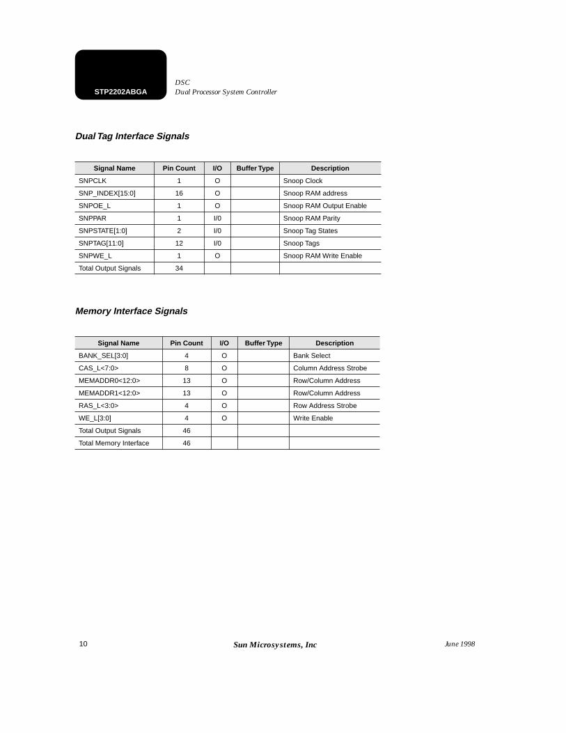
Dual Tag Interface Signals
Memory Interface Signals
Signal Name Pin Count I/O Buffer Type Description
SNPCLK 1 O Snoop Clock
SNP_INDEX[15:0] 16 O Snoop RAM address
SNPOE_L 1 O Snoop RAM Output Enable
SNPPAR 1 I/0 Snoop RAM Parity
SNPSTATE[1:0] 2 I/0 Snoop Tag States
SNPTAG[11:0] 12 I/0 Snoop Tags
SNPWE_L 1 O Snoop RAM Write Enable
Total Output Signals 34
Signal Name Pin Count I/O Buffer Type Description
BANK_SEL[3:0] 4 O Bank Select
CAS_L<7:0> 8 O Column Address Strobe
MEMADDR0<12:0> 13 O Row/Column Address
MEMADDR1<12:0> 13 O Row/Column Address
RAS_L<3:0> 4 O Row Address Strobe
WE_L[3:0] 4 O Write Enable
Total Output Signals 46
Total Memory Interface 46
11
Dual Processor System ControllerDSC
STP2202ABGA
June 1998
Sun Microsystems, Inc
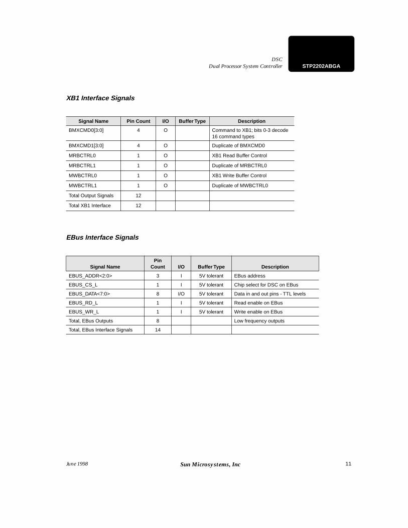
XB1 Interface Signals
EBus Interface Signals
Signal Name Pin Count I/O Buffer Type Description
BMXCMD0[3:0] 4 O Command to XB1; bits 0-3 decode 16 command types
BMXCMD1[3:0] 4 O Duplicate of BMXCMD0
MRBCTRL0 1 O XB1 Read Buffer Control
MRBCTRL1 1 O Duplicate of MRBCTRL0
MWBCTRL0 1 O XB1 Write Buffer Control
MWBCTRL1 1 O Duplicate of MWBCTRL0
Total Output Signals 12
Total XB1 Interface 12
Signal NamePin
Count I/O Buffer Type Description
EBUS_ADDR<2:0> 3 I 5V tolerant EBus address
EBUS_CS_L 1 I 5V tolerant Chip select for DSC on EBus
EBUS_DATA<7:0> 8 I/O 5V tolerant Data in and out pins - TTL levels
EBUS_RD_L 1 I 5V tolerant Read enable on EBus
EBUS_WR_L 1 I 5V tolerant Write enable on EBus
Total, EBus Outputs 8 Low frequency outputs
Total, EBus Interface Signals 14
12
STP2202ABGA
Dual Processor System Controller DSC
June 1998
Sun Microsystems, Inc
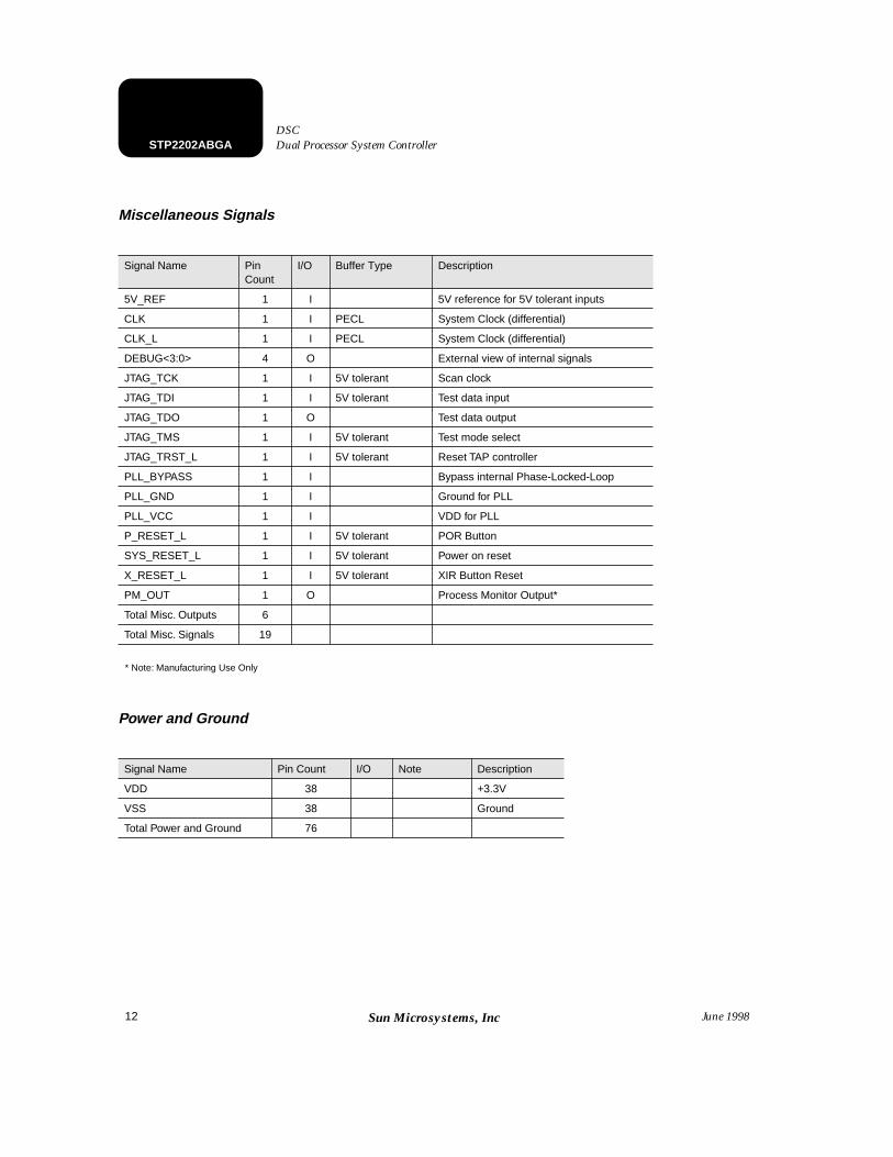
Miscellaneous Signals
* Note: Manufacturing Use Only
Power and Ground
Signal Name Pin Count
I/O Buffer Type Description
5V_REF 1 I 5V reference for 5V tolerant inputs
CLK 1 I PECL System Clock (differential)
CLK_L 1 I PECL System Clock (differential)
DEBUG<3:0> 4 O External view of internal signals
JTAG_TCK 1 I 5V tolerant Scan clock
JTAG_TDI 1 I 5V tolerant Test data input
JTAG_TDO 1 O Test data output
JTAG_TMS 1 I 5V tolerant Test mode select
JTAG_TRST_L 1 I 5V tolerant Reset TAP controller
PLL_BYPASS 1 I Bypass internal Phase-Locked-Loop
PLL_GND 1 I Ground for PLL
PLL_VCC 1 I VDD for PLL
P_RESET_L 1 I 5V tolerant POR Button
SYS_RESET_L 1 I 5V tolerant Power on reset
X_RESET_L 1 I 5V tolerant XIR Button Reset
PM_OUT 1 O Process Monitor Output*
Total Misc. Outputs 6
Total Misc. Signals 19
Signal Name Pin Count I/O Note Description
VDD 38 +3.3V
VSS 38 Ground
Total Power and Ground 76
13
Dual Processor System ControllerDSC
STP2202ABGA
June 1998
Sun Microsystems, Inc
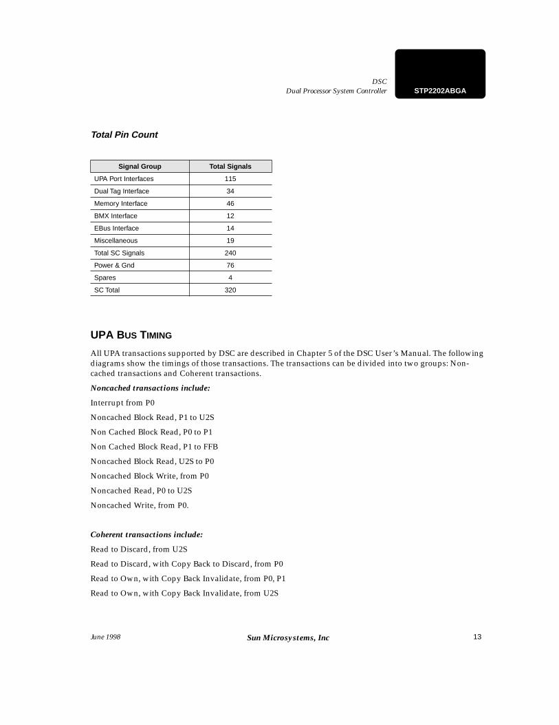
Total Pin Count
UPA B
US
T
IMING
All UPA transactions supported by DSC are described in Chapter 5 of the DSC User’s Manual. The following diagrams show the timings of those transactions. The transactions can be divided into two groups: Non-cached transactions and Coherent transactions.
Noncached transactions include:
Interrupt from P0
Noncached Block Read, P1 to U2S
Non Cached Block Read, P0 to P1
Non Cached Block Read, P1 to FFB
Noncached Block Read, U2S to P0
Noncached Block Write, from P0
Noncached Read, P0 to U2S
Noncached Write, from P0.
Coherent transactions include:
Read to Discard, from U2S
Read to Discard, with Copy Back to Discard, from P0
Read to Own, with Copy Back Invalidate, from P0, P1
Read to Own, with Copy Back Invalidate, from U2S
Signal Group Total Signals
UPA Port Interfaces 115
Dual Tag Interface 34
Memory Interface 46
BMX Interface 12
EBus Interface 14
Miscellaneous 19
Total SC Signals 240
Power & Gnd 76
Spares 4
SC Total 320
14
STP2202ABGA
Dual Processor System Controller DSC
June 1998
Sun Microsystems, Inc
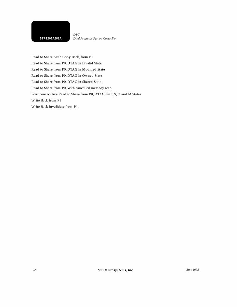
Read to Share, with Copy Back, from P1
Read to Share from P0, DTAG in Invalid State
Read to Share from P0, DTAG in Modified State
Read to Share from P0, DTAG in Owned State
Read to Share from P0, DTAG in Shared State
Read to Share from P0, With cancelled memory read
Four consecutive Read to Share from P0, DTAGS in I, S, O and M States
Write Back from P1
Write Back Invalidate from P1.
15
Dual Processor System ControllerDSC
STP2202ABGA
June 1998
Sun Microsystems, Inc
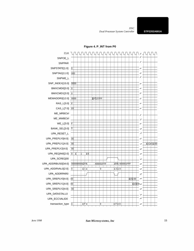
Figure 4. P_INT from P0
0
000
CLK
SNPOE_L
SNPPAR
SNPSTATE[1:0]
SNPTAG[11:0]
SNPWE_L
SNP_INDEX[15:0] 0000
BMXCMD0[3:0] 0
BMXCMD1[3:0] 0
MEMADDR0[12:0] 1F* 07FF0000
RAS_L[3:0] F
CAS_L[7:0] FF
ME_MRBCtrl
ME_MWBCtrl
WE_L[3:0] F
BANK_SEL[3:0]
UPA_RESET_L
UPA_PREPLY0[4:0] 00
UPA_PREPLY1[4:0] 1C 01 0000
UPA_PREPLY2[4:0] 00
UPA_REQIN0[2:0] 00 1
UPA_SCREQ00
UPA_ADDRBUS0[34:0] 000000000 7F* 7F*400001FFF 400001FFF
UPA_ADDRVAL0[2:0] 0 0 021
UPA_ADDRPAR0
UPA_SREPLY0[4:0] 00 0015
UPA_SREPLY1[4:0] 0000 1D
UPA_SREPLY2[4:0] 00
UPA_DATASTALL0
UPA_ECCVALID0
transaction_type 000 F F
0
16
STP2202ABGA
Dual Processor System Controller DSC
June 1998
Sun Microsystems, Inc
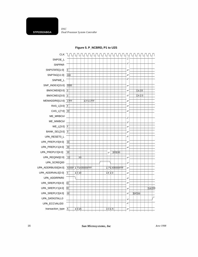
Figure 5. P_NCBRD, P1 to U2S
0
000
CLK
SNPOE_L
SNPPAR
SNPSTATE[1:0]
SNPTAG[11:0]
SNPWE_L
SNP_INDEX[15:0] 0000
BMXCMD0[3:0] 0
BMXCMD1[3:0] 0
MEMADDR0[12:0] 1* 17FF17FF
RAS_L[3:0] F
CAS_L[7:0] FF
ME_MRBCtrl
ME_MWBCtrl
WE_L[3:0] F
BANK_SEL[3:0]
UPA_RESET0_L
UPA_PREPLY0[4:0] 00
UPA_PREPLY1[4:0] 00
UPA_PREPLY2[4:0] 00
UPA_REQIN0[2:0] 02
UPA_SCREQ00
UPA_ADDRBUS0[34:0] 41555* 7* 7* 435555FFF
UPA_ADDRVAL0[2:0] 0 02
UPA_ADDRPAR0
UPA_SREPLY0[4:0] 00
UPA_SREPLY1[4:0] 00
UPA_SREPLY2[4:0] 00
UPA_DATASTALL0
UPA_ECCVALID0
transaction_type 00A A A
0
0
A
A
0
0003
435555FFF
0 4
0018
000F
17
Dual Processor System ControllerDSC
STP2202ABGA
June 1998 Sun Microsystems, Inc
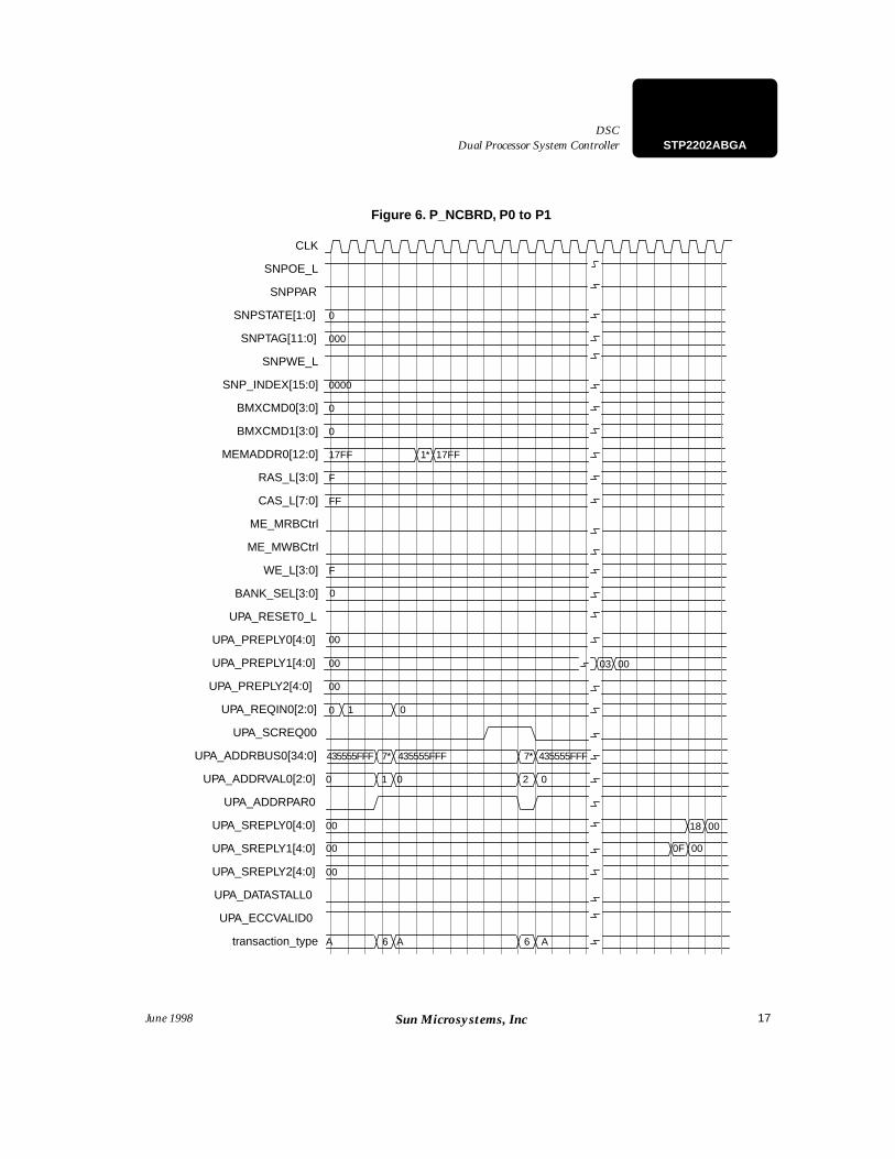
Figure 6. P_NCBRD, P0 to P1
0
000
CLK
SNPOE_L
SNPPAR
SNPSTATE[1:0]
SNPTAG[11:0]
SNPWE_L
SNP_INDEX[15:0] 0000
BMXCMD0[3:0] 0
BMXCMD1[3:0] 0
MEMADDR0[12:0] 1* 17FF17FF
RAS_L[3:0] F
CAS_L[7:0] FF
ME_MRBCtrl
ME_MWBCtrl
WE_L[3:0] F
BANK_SEL[3:0]
UPA_RESET0_L
UPA_PREPLY0[4:0] 00
UPA_PREPLY1[4:0] 00
UPA_PREPLY2[4:0] 00
UPA_REQIN0[2:0] 01
UPA_SCREQ00
UPA_ADDRBUS0[34:0] 435555FFF 7* 7* 435555FFF
UPA_ADDRVAL0[2:0] 0 01
UPA_ADDRPAR0
UPA_SREPLY0[4:0] 00
UPA_SREPLY1[4:0] 00
UPA_SREPLY2[4:0] 00
UPA_DATASTALL0
UPA_ECCVALID0
transaction_type 66A A A
0
00
435555FFF
0 2
000F
0
0018
03
18
STP2202ABGA Dual Processor System Controller DSC
June 1998Sun Microsystems, Inc
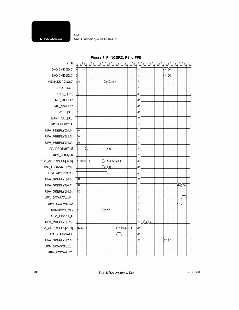
Figure 7. P_NCBRD, P1 to FFB
CLK
BMXCMD0[3:0]
BMXCMD1[3:0]
MEMADDR0[12:0]
RAS_L[3:0]
CAS_L[7:0]
ME_MRBCtrl
ME_MWBCtrl
WE_L[3:0]
BANK_SEL[3:0]
UPA_RESET0_L
UPA_PREPLY0[4:0]
UPA_PREPLY1[4:0]
UPA_PREPLY2[4:0]
UPA_REQIN0[2:0]
UPA_SREQ00
UPA_ADDRBUS0[34:0]
UPA_ADDRVAL0[2:0]
UPA_ADDRPAR0
UPA_SREPLY0[4:0]
UPA_SREPLY1[4:0]
UPA_SREPLY2[4:0]
UPA_DATASTALL0
UPA_ECCVALID0
transaction_type
UPA_RESET_L
UPA_PREPLY3[1:0]
UPA_ADDRBUS1[28:0]
UPA_ADDRVAL1
UPA_SREPLY3[2:0]
UPA_DATASTALL1
UPA_ECCVALID1
F
1* 17FF17FF
00
0
00
A 0 A
0A0
0A0
FF
F
0
00
00
2 0
415555FFF 7* 435555FFF
0 2 0
00 0018
00
0 03
15555FFF 7* 15555FFF
070
19
Dual Processor System ControllerDSC
STP2202ABGA
June 1998 Sun Microsystems, Inc
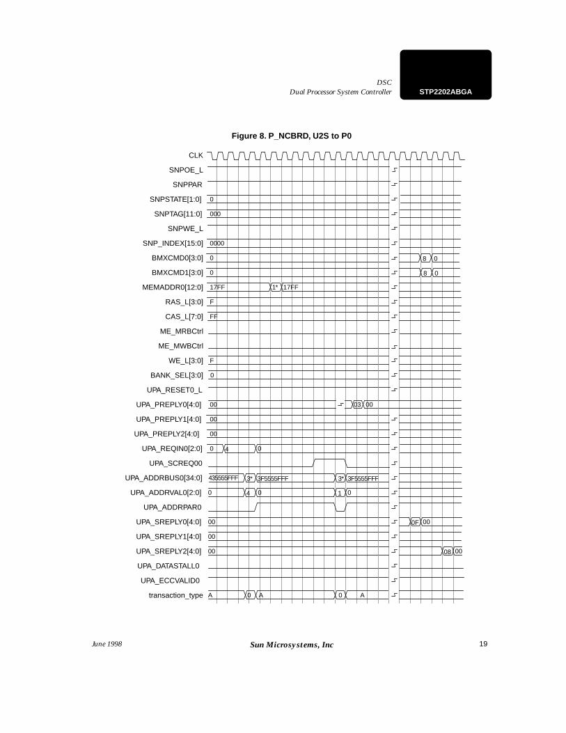
Figure 8. P_NCBRD, U2S to P0
0
000
CLK
SNPOE_L
SNPPAR
SNPSTATE[1:0]
SNPTAG[11:0]
SNPWE_L
SNP_INDEX[15:0] 0000
BMXCMD0[3:0] 0
BMXCMD1[3:0] 0
MEMADDR0[12:0] 1* 17FF17FF
RAS_L[3:0] F
CAS_L[7:0] FF
ME_MRBCtrl
ME_MWBCtrl
WE_L[3:0] F
BANK_SEL[3:0]
UPA_RESET0_L
UPA_PREPLY0[4:0] 00
UPA_PREPLY1[4:0] 00
UPA_PREPLY2[4:0] 00
UPA_REQIN0[2:0] 04
UPA_SCREQ00
UPA_ADDRBUS0[34:0] 435555FFF 3* 3* 3F5555FFF
UPA_ADDRVAL0[2:0] 0 04
UPA_ADDRPAR0
UPA_SREPLY0[4:0] 00
UPA_SREPLY1[4:0] 00
UPA_SREPLY2[4:0] 00
UPA_DATASTALL0
UPA_ECCVALID0
transaction_type 00A A A
0
00
3F5555FFF
0 1
0008
0
000F
03
08
08
20
STP2202ABGA Dual Processor System Controller DSC
June 1998Sun Microsystems, Inc
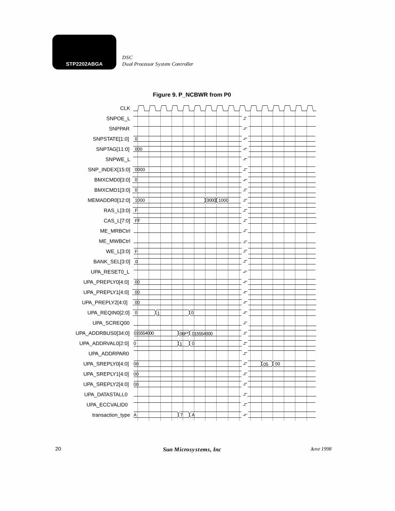
Figure 9. P_NCBWR from P0
0
000
CLK
SNPOE_L
SNPPAR
SNPSTATE[1:0]
SNPTAG[11:0]
SNPWE_L
SNP_INDEX[15:0] 0000
BMXCMD0[3:0] 0
BMXCMD1[3:0] 0
MEMADDR0[12:0] 0000 10001000
RAS_L[3:0] F
CAS_L[7:0] FF
ME_MRBCtrl
ME_MWBCtrl
WE_L[3:0] F
BANK_SEL[3:0]
UPA_RESET0_L
UPA_PREPLY0[4:0] 00
UPA_PREPLY1[4:0] 00
UPA_PREPLY2[4:0] 00
UPA_REQIN0[2:0] 01
UPA_SCREQ00
UPA_ADDRBUS0[34:0] 015554000 06F*
UPA_ADDRVAL0[2:0] 0 1
UPA_ADDRPAR0
UPA_SREPLY0[4:0] 00
UPA_SREPLY1[4:0] 00
UPA_SREPLY2[4:0] 00
UPA_DATASTALL0
UPA_ECCVALID0
transaction_type 7A A
0
015554000
0
0
0005
21
Dual Processor System ControllerDSC
STP2202ABGA
June 1998 Sun Microsystems, Inc
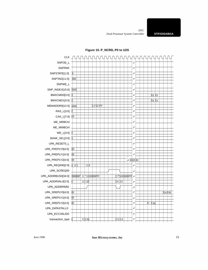
Figure 10. P_NCRD, P0 to U2S
0
000
CLK
SNPOE_L
SNPPAR
SNPSTATE[1:0]
SNPTAG[11:0]
SNPWE_L
SNP_INDEX[15:0] 0000
BMXCMD0[3:0] 0
BMXCMD1[3:0] 0
MEMADDR0[12:0] 1* 17FF0000
RAS_L[3:0] F
CAS_L[7:0] FF
ME_MRBCtrl
ME_MWBCtrl
WE_L[3:0] F
BANK_SEL[3:0]
UPA_RESET0_L
UPA_PREPLY0[4:0] 00
UPA_PREPLY1[4:0] 00
UPA_PREPLY2[4:0] 00
UPA_REQIN0[2:0] 01
UPA_SCREQ00
UPA_ADDRBUS0[34:0] 0000000* * 7* 415555FFF
UPA_ADDRVAL0[2:0] 0 01
UPA_ADDRPAR0
UPA_SREPLY0[4:0] 00
UPA_SREPLY1[4:0] 00
UPA_SREPLY2[4:0] 00
UPA_DATASTALL0
UPA_ECCVALID0
transaction_type 550 A A
0
415555FFF
0 4
0
001A
09
09
0003
00*
22
STP2202ABGA Dual Processor System Controller DSC
June 1998Sun Microsystems, Inc
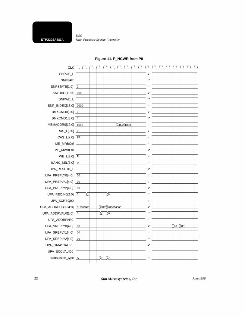
Figure 11. P_NCWR from P0
0
000
CLK
SNPOE_L
SNPPAR
SNPSTATE[1:0]
SNPTAG[11:0]
SNPWE_L
SNP_INDEX[15:0] 0000
BMXCMD0[3:0] 0
BMXCMD1[3:0] 0
MEMADDR0[12:0] 0000 10001000
RAS_L[3:0] F
CAS_L[7:0] FF
ME_MRBCtrl
ME_MWBCtrl
WE_L[3:0] F
BANK_SEL[3:0]
UPA_RESET0_L
UPA_PREPLY0[4:0] 00
UPA_PREPLY1[4:0] 00
UPA_PREPLY2[4:0] 00
UPA_REQIN0[2:0] 01
UPA_SCREQ00
UPA_ADDRBUS0[34:0] 015554000 07D0*
UPA_ADDRVAL0[2:0] 0 1
UPA_ADDRPAR0
UPA_SREPLY0[4:0] 00
UPA_SREPLY1[4:0] 00
UPA_SREPLY2[4:0] 00
UPA_DATASTALL0
UPA_ECCVALID0
transaction_type EA A
0
015554000
0
0
0004

23
Dual Processor System ControllerDSC
STP2202ABGA
June 1998 Sun Microsystems, Inc
Figure 12. P_RDD from U2S
8*
0
801
CLK
SNPOE_L
SNPPAR
SNPSTATE[1:0]
SNPTAG[11:0]
SNPWE_L
SNP_INDEX[15:0] 0000
BMXCMD0[3:0] 0
BMXCMD1[3:0] 0
MEMADDR0[12:0] 0008 000017FF
RAS_L[3:0] F
CAS_L[7:0] FF
ME_MRBCtrl
ME_MWBCtrl
WE_L[3:0] F
BANK_SEL[3:0]
UPA_RESET0_L
UPA_PREPLY0[4:0] 00
UPA_PREPLY1[4:0] 00
UPA_PREPLY2[4:0] 00
UPA_REQIN0[2:0] 04
UPA_SCREQ00
UPA_ADDRBUS0[34:0] 415555FFF 0* 3E0000000
UPA_ADDRVAL0[2:0] 0 04
UPA_ADDRPAR0
UPA_SREPLY0[4:0] 00
UPA_SREPLY1[4:0] 00
UPA_SREPLY2[4:0] 00
UPA_DATASTALL0
UPA_ECCVALID0
transaction_type 53A 0 A
0
3E0000000
0 4
0
3 0
802
0000
1800 1* 17FF
B F
CF FF
F 0
04
0* 3* 3F5555FFF
01
D 0
24
STP2202ABGA Dual Processor System Controller DSC
June 1998Sun Microsystems, Inc
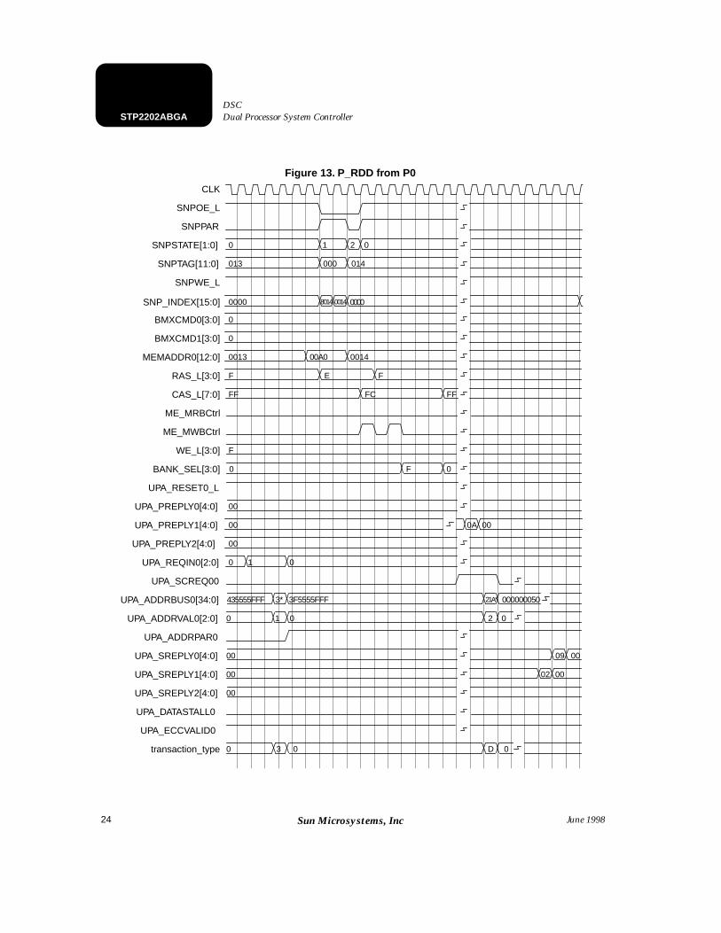
Figure 13. P_RDD from P0
0
013
CLK
SNPOE_L
SNPPAR
SNPSTATE[1:0]
SNPTAG[11:0]
SNPWE_L
SNP_INDEX[15:0] 0000
BMXCMD0[3:0] 0
BMXCMD1[3:0] 0
MEMADDR0[12:0] 00A0 00140013
RAS_L[3:0] F
CAS_L[7:0] FF
ME_MRBCtrl
ME_MWBCtrl
WE_L[3:0] F
BANK_SEL[3:0]
UPA_RESET0_L
UPA_PREPLY0[4:0] 00
UPA_PREPLY1[4:0] 00
UPA_PREPLY2[4:0] 00
UPA_REQIN0[2:0] 01
UPA_SCREQ00
UPA_ADDRBUS0[34:0] 435555FFF 3* 21A* 000000050
UPA_ADDRVAL0[2:0] 0 01
UPA_ADDRPAR0
UPA_SREPLY0[4:0] 00
UPA_SREPLY1[4:0] 00
UPA_SREPLY2[4:0] 00
UPA_DATASTALL0
UPA_ECCVALID0
transaction_type D30 0 0
0
3F5555FFF
0 2
0002
0
0009
2 01
000 014
8014 0014 0000
E F
FFFC
F 0
0A 00
25
Dual Processor System ControllerDSC
STP2202ABGA
June 1998 Sun Microsystems, Inc
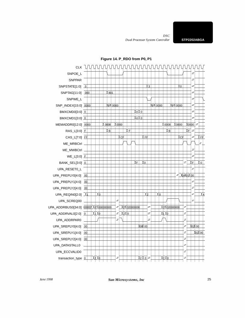
Figure 14. P_RDO from P0, P1
0
000
CLK
SNPOE_L
SNPPAR
SNPSTATE[1:0]
SNPTAG[11:0]
SNPWE_L
SNP_INDEX[15:0] 0000
BMXCMD0[3:0] 0
BMXCMD1[3:0]
MEMADDR0[12:0] 00080000
RAS_L[3:0] F
CAS_L[7:0] FF
ME_MRBCtrl
ME_MWBCtrl
WE_L[3:0] F
BANK_SEL[3:0]
UPA_RESET0_L
UPA_PREPLY0[4:0] 00
UPA_PREPLY1[4:0] 00
UPA_PREPLY2[4:0]
UPA_REQIN0[2:0] 0 4
UPA_SCREQ00
UPA_ADDRBUS0[34:0] 000000* 0* 020000000
UPA_ADDRVAL0[2:0] 0 01
UPA_ADDRPAR0
UPA_SREPLY0[4:0] 00
UPA_SREPLY1[4:0] 00
UPA_SREPLY2[4:0] 00
UPA_DATASTALL0
UPA_ECCVALID0
transaction_type C20 0 0
0
000000000
0 1
1
3 0
801
0000 0000
B F
CF FF
F 0
02
0* 0*
02
2 0
8* 00008* 00008* 0000
4 0
0 4 0
0008 0800
B F
CF FF
F 0
00010A
00
020000000
08 00 02 00
02 00
26
STP2202ABGA Dual Processor System Controller DSC
June 1998Sun Microsystems, Inc
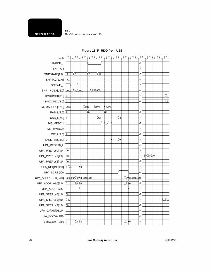
Figure 15. P_RDO from U2S
0
801
CLK
SNPOE_L
SNPPAR
SNPSTATE[1:0]
SNPTAG[11:0]
SNPWE_L
SNP_INDEX[15:0] 0000
BMXCMD0[3:0] 0
BMXCMD1[3:0]
MEMADDR0[12:0] 00080000
RAS_L[3:0] F
CAS_L[7:0] FF
ME_MRBCtrl
ME_MWBCtrl
WE_L[3:0] F
BANK_SEL[3:0]
UPA_RESET0_L
UPA_PREPLY0[4:0]
00UPA_PREPLY1[4:0]
00
UPA_PREPLY2[4:0]
UPA_REQIN0[2:0] 0 4
UPA_SCREQ00
UPA_ADDRBUS0[34:0] 020000* 0*
UPA_ADDRVAL0[2:0] 0 4
UPA_ADDRPAR0
UPA_SREPLY0[4:0] 00
UPA_SREPLY1[4:0] 00
UPA_SREPLY2[4:0] 00
UPA_DATASTALL0
UPA_ECCVALID0
transaction_type 20 8
0
3F0000000
0
3 0
1800
B F
CF FF
F 0
0
0*
02
C 0
8* 0000
8
001F0A
00
3E0000000
02 00
3
8* 0000
0 8
0000
27
Dual Processor System ControllerDSC
STP2202ABGA
June 1998 Sun Microsystems, Inc
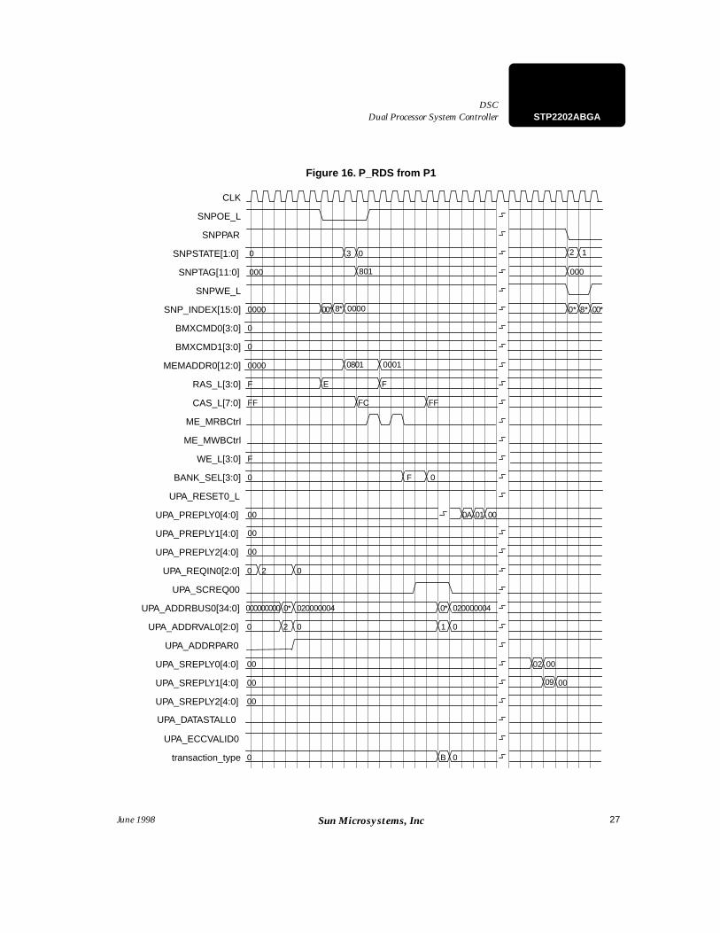
Figure 16. P_RDS from P1
0
000
CLK
SNPOE_L
SNPPAR
SNPSTATE[1:0]
SNPTAG[11:0]
SNPWE_L
SNP_INDEX[15:0] 0000
BMXCMD0[3:0] 0
BMXCMD1[3:0]
MEMADDR0[12:0] 0000
RAS_L[3:0] F
CAS_L[7:0] FF
ME_MRBCtrl
ME_MWBCtrl
WE_L[3:0] F
BANK_SEL[3:0]
UPA_RESET0_L
UPA_PREPLY0[4:0] 00
UPA_PREPLY1[4:0] 00
UPA_PREPLY2[4:0]
UPA_REQIN0[2:0] 0 2
UPA_SCREQ00
UPA_ADDRBUS0[34:0] 000000000 0*
UPA_ADDRVAL0[2:0] 0 2
UPA_ADDRPAR0
UPA_SREPLY0[4:0] 00
UPA_SREPLY1[4:0] 00
UPA_SREPLY2[4:0] 00
UPA_DATASTALL0
UPA_ECCVALID0
transaction_type 0
0
020000004
0
3 0
0801
E F
FC FF
F 0
0
0*
01
B 0
00*
000A 01
00
020000004
02
00
1
8* 0000
0
0001
2
801 000
0* 8* 00*
00
09
28
STP2202ABGA Dual Processor System Controller DSC
June 1998Sun Microsystems, Inc
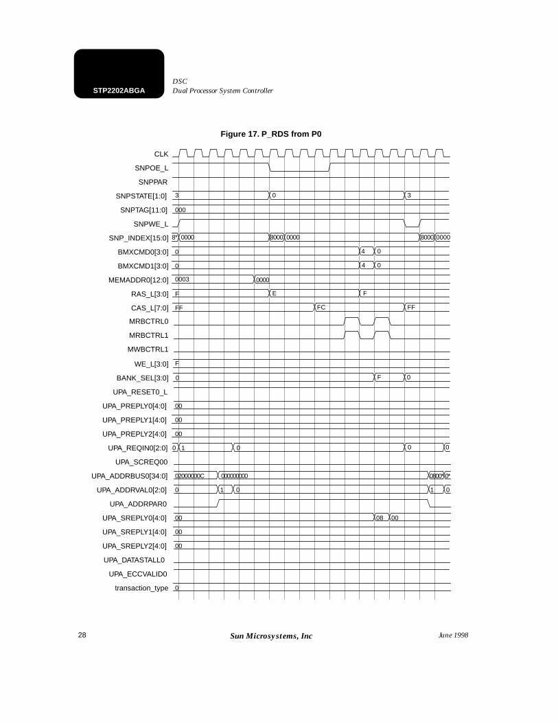
Figure 17. P_RDS from P0
3
000
CLK
SNPOE_L
SNPPAR
SNPSTATE[1:0]
SNPTAG[11:0]
SNPWE_L
SNP_INDEX[15:0] 0000
BMXCMD0[3:0] 0
BMXCMD1[3:0] 0
MEMADDR0[12:0] 00000003
RAS_L[3:0] F
CAS_L[7:0] FF
MRBCTRL0
MRBCTRL1
WE_L[3:0] F
BANK_SEL[3:0]
UPA_RESET0_L
UPA_PREPLY0[4:0] 00
UPA_PREPLY1[4:0] 00
UPA_PREPLY2[4:0] 00
UPA_REQIN0[2:0] 01
UPA_SCREQ00
UPA_ADDRBUS0[34:0] 02000000C 000000000
UPA_ADDRVAL0[2:0] 0 1
UPA_ADDRPAR0
UPA_SREPLY0[4:0] 00
UPA_SREPLY1[4:0] 00
UPA_SREPLY2[4:0] 00
UPA_DATASTALL0
UPA_ECCVALID0
transaction_type 0
0
0800*
0
0
0008
0 3
8* 8000 80000000 0000
04
04
E F
FC FF
MWBCTRL1
F 0
0 0
0*
01
29
Dual Processor System ControllerDSC
STP2202ABGA
June 1998 Sun Microsystems, Inc
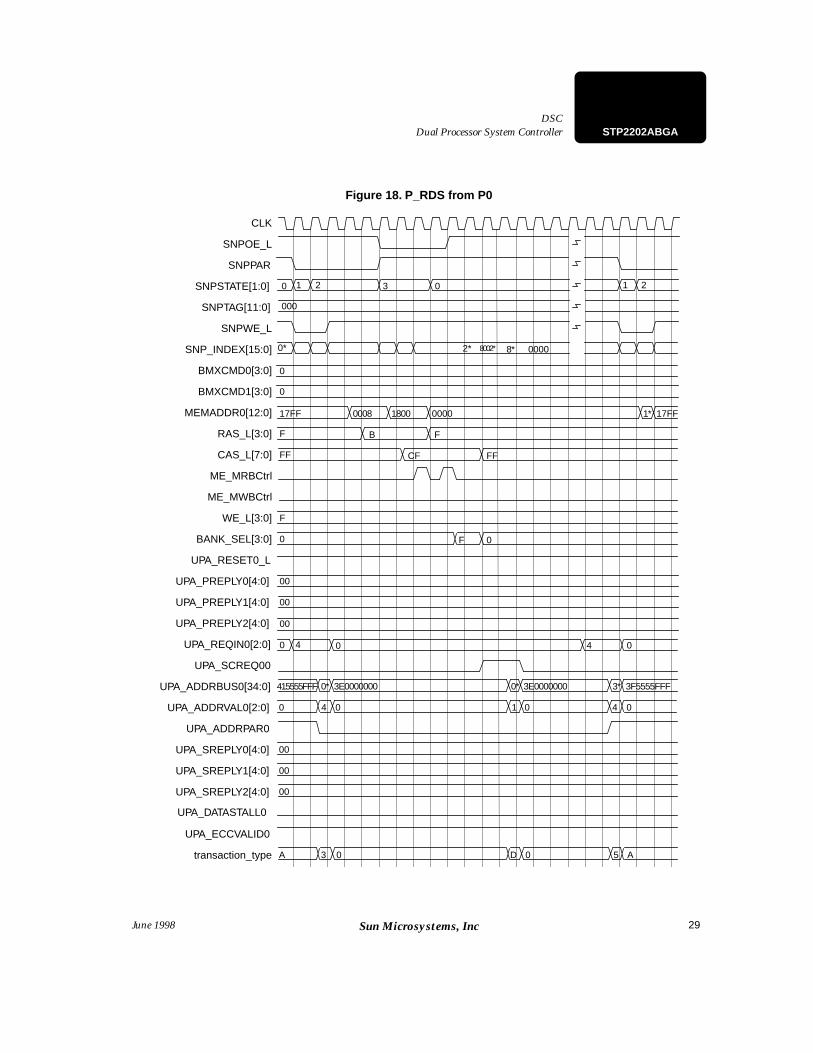
Figure 18. P_RDS from P0
8*
0
000
CLK
SNPOE_L
SNPPAR
SNPSTATE[1:0]
SNPTAG[11:0]
SNPWE_L
SNP_INDEX[15:0] 0*
BMXCMD0[3:0] 0
BMXCMD1[3:0] 0
MEMADDR0[12:0] 0008 000017FF
RAS_L[3:0] F
CAS_L[7:0] FF
ME_MRBCtrl
ME_MWBCtrl
WE_L[3:0] F
BANK_SEL[3:0]
UPA_RESET0_L
UPA_PREPLY0[4:0] 00
UPA_PREPLY1[4:0] 00
UPA_PREPLY2[4:0] 00
UPA_REQIN0[2:0] 04
UPA_SCREQ00
UPA_ADDRBUS0[34:0] 415555FFF 0* 3E0000000
UPA_ADDRVAL0[2:0] 0 04
UPA_ADDRPAR0
UPA_SREPLY0[4:0] 00
UPA_SREPLY1[4:0] 00
UPA_SREPLY2[4:0] 00
UPA_DATASTALL0
UPA_ECCVALID0
transaction_type 53A 0 A
0
3E0000000
0 4
0
3 0
0000
1800 1* 17FF
B F
CF FF
F 0
04
0* 3* 3F5555FFF
01
D 0
1 2 1 2
8002*2*
30
STP2202ABGA Dual Processor System Controller DSC
June 1998Sun Microsystems, Inc
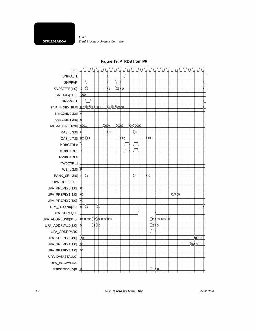
Figure 19. P_RDS from P0
8*
0
000
CLK
SNPOE_L
SNPPAR
SNPSTATE[1:0]
SNPTAG[11:0]
SNPWE_L
SNP_INDEX[15:0] 00*
BMXCMD0[3:0] 0
BMXCMD1[3:0] 0
MEMADDR0[12:0] 0000 00020001
RAS_L[3:0] F
CAS_L[7:0] FC
MRBCTRL0
MRBCTRL1
WE_L[3:0] F
BANK_SEL[3:0]
UPA_RESET0_L
UPA_PREPLY0[4:0] 00
UPA_PREPLY1[4:0] 00
UPA_PREPLY2[4:0] 00
UPA_REQIN0[2:0] 01
UPA_SCREQ00
UPA_ADDRBUS0[34:0] 0000000* 1*
UPA_ADDRVAL0[2:0] 0 1
UPA_ADDRPAR0
UPA_SREPLY0[4:0] 00
UPA_SREPLY1[4:0] 00
UPA_SREPLY2[4:0] 00
UPA_DATASTALL0
UPA_ECCVALID0
transaction_type 0
0
000000008
0
0
3 0
0000
0002
E F
FC FF
F 0
1*
02
B 0
2
00* 8* 0000 00*
0*
FF
MWBCTRL0
MWBCTRL1
F
0A 00
000000008
09 00
02 00
1
31
Dual Processor System ControllerDSC
STP2202ABGA
June 1998 Sun Microsystems, Inc
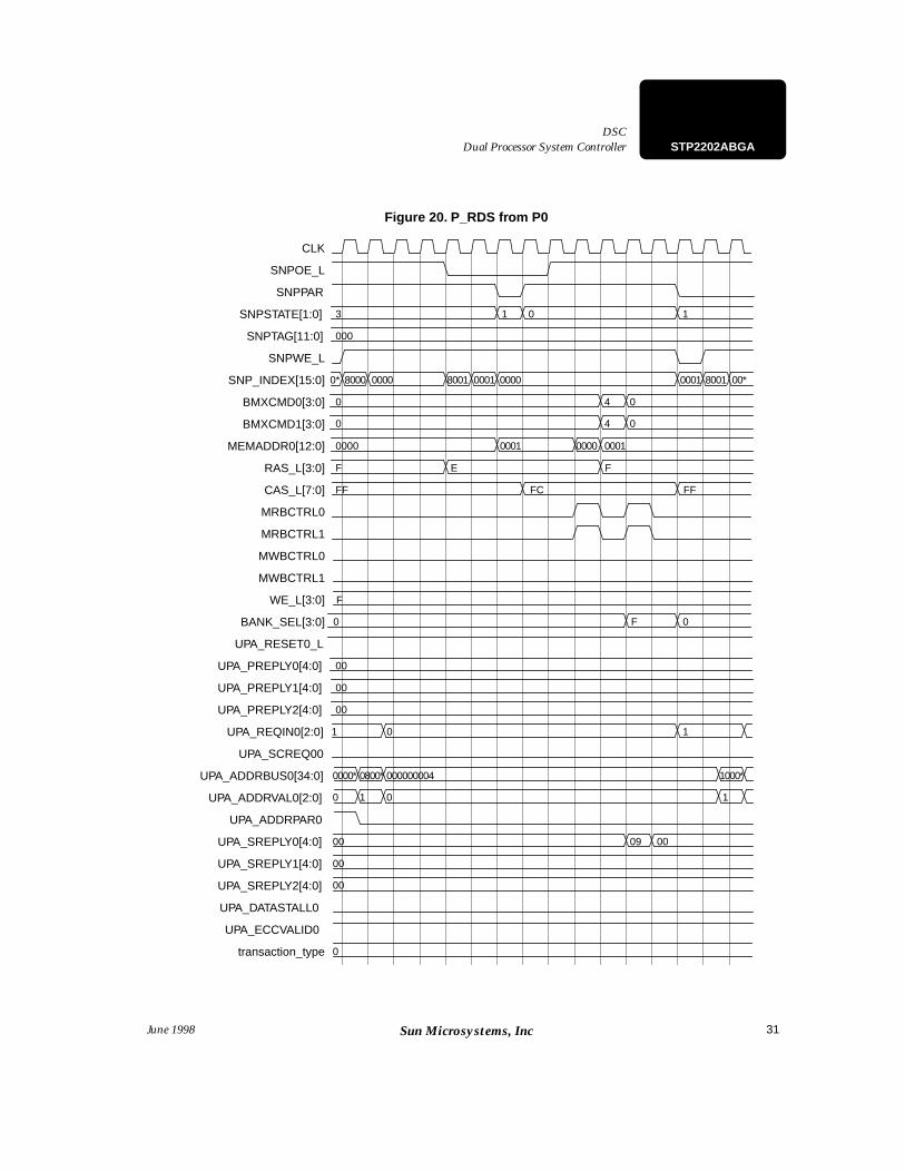
Figure 20. P_RDS from P0
3
000
CLK
SNPOE_L
SNPPAR
SNPSTATE[1:0]
SNPTAG[11:0]
SNPWE_L
SNP_INDEX[15:0] 0000
BMXCMD0[3:0] 0
BMXCMD1[3:0]
MEMADDR0[12:0] 0001 00000000
RAS_L[3:0] F
CAS_L[7:0] FF
MRBCTRL0
MRBCTRL1
WE_L[3:0]
BANK_SEL[3:0]
UPA_RESET0_L
UPA_PREPLY0[4:0]
UPA_PREPLY1[4:0]
00
UPA_PREPLY2[4:0]
00
UPA_REQIN0[2:0]
UPA_SCREQ00
UPA_ADDRBUS0[34:0] 0000* 0800*
UPA_ADDRVAL0[2:0]
UPA_ADDRPAR0
UPA_SREPLY0[4:0] 00
UPA_SREPLY1[4:0]
UPA_SREPLY2[4:0]
00
UPA_DATASTALL0
UPA_ECCVALID0
transaction_type 0
F
000000004
00
0009
MWBCTRL0
MWBCTRL1
1 0 1
80000* 8001 0001 0000 0001 8001 00*
4 0
0 4 0
0001
E F
FC FF
0 0F
1 10
1000*
0 1 0 1
00
32
STP2202ABGA Dual Processor System Controller DSC
June 1998Sun Microsystems, Inc
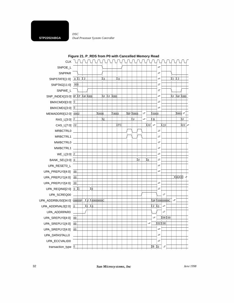
Figure 21. P_RDS from P0 with Cancelled Memory Read
0
000
CLK
SNPOE_L
SNPPAR
SNPSTATE[1:0]
SNPTAG[11:0]
SNPWE_L
SNP_INDEX[15:0] 00*
BMXCMD0[3:0] 0
BMXCMD1[3:0] 0
MEMADDR0[12:0] 000300000002
RAS_L[3:0] F
CAS_L[7:0] FF
MRBCTRL0
MRBCTRL1
WE_L[3:0] F
BANK_SEL[3:0]
UPA_RESET0_L
UPA_PREPLY0[4:0] 00
UPA_PREPLY1[4:0] 00
UPA_PREPLY2[4:0] 00
UPA_REQIN0[2:0] 01
UPA_SCREQ00
UPA_ADDRBUS0[34:0] 0000000* 1* 00000000C
UPA_ADDRVAL0[2:0] 0 1
UPA_ADDRPAR0
UPA_SREPLY0[4:0] 00
UPA_SREPLY1[4:0] 00
UPA_SREPLY2[4:0] 00
UPA_DATASTALL0
UPA_ECCVALID0
transaction_type 0
0
00000000C
0
0
3 0
0003 0000
E F
FC FF
F 0
19*
02
B 0
1 2 1 2
80*0* 0000 8* 0* 0000 0* 80* 0000
00*
MWBCTRL0
MWBCTRL1
0A 00
09 00
02 00
0003
FB
FFCF
33
Dual Processor System ControllerDSC
STP2202ABGA
June 1998 Sun Microsystems, Inc
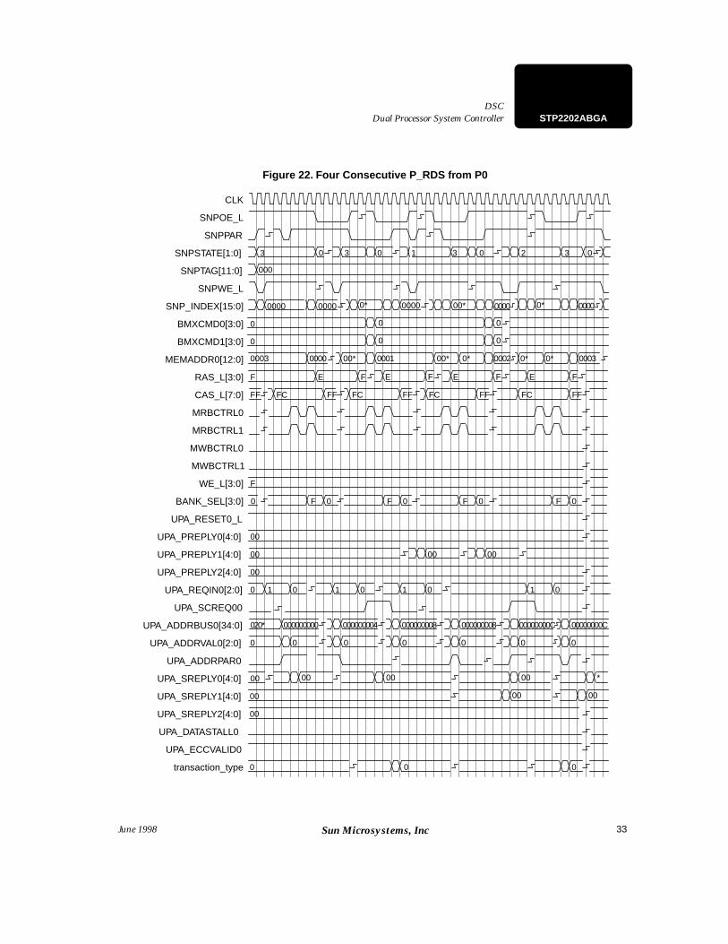
Figure 22. Four Consecutive P_RDS from P0
0
000
CLK
SNPOE_L
SNPPAR
SNPSTATE[1:0]
SNPTAG[11:0]
SNPWE_L
SNP_INDEX[15:0] 0*
BMXCMD0[3:0] 0
BMXCMD1[3:0]
MEMADDR0[12:0] 0000 00020003
RAS_L[3:0] F
CAS_L[7:0] FF
MRBCTRL0
MRBCTRL1
WE_L[3:0] F
BANK_SEL[3:0]
UPA_RESET0_L
UPA_PREPLY0[4:0] 00
UPA_PREPLY1[4:0] 00
UPA_PREPLY2[4:0] 00
UPA_REQIN0[2:0] 01
UPA_SCREQ00
UPA_ADDRBUS0[34:0] 020*
UPA_ADDRVAL0[2:0]
UPA_ADDRPAR0
UPA_SREPLY0[4:0] 00
UPA_SREPLY1[4:0] 00
UPA_SREPLY2[4:0] 00
UPA_DATASTALL0
UPA_ECCVALID0
transaction_type 0
0
000000000
0
3 0
0000
E F
0
0 0
3
0000
FC
MWBCTRL0
MWBCTRL1
F
00
000000004
*
1 203 03
0000 00* 0000 0* 0000
00
0 00
0001 00* 0*00* 00030* 0*
E F E F E F
FF FC FF FC FF FC FF
0F 0F 0F
00
0101 01
000000008 000000008 00000000C 00000000C
0 0 0 0 0 0 0
00 00 00
0000
34
STP2202ABGA Dual Processor System Controller DSC
June 1998Sun Microsystems, Inc
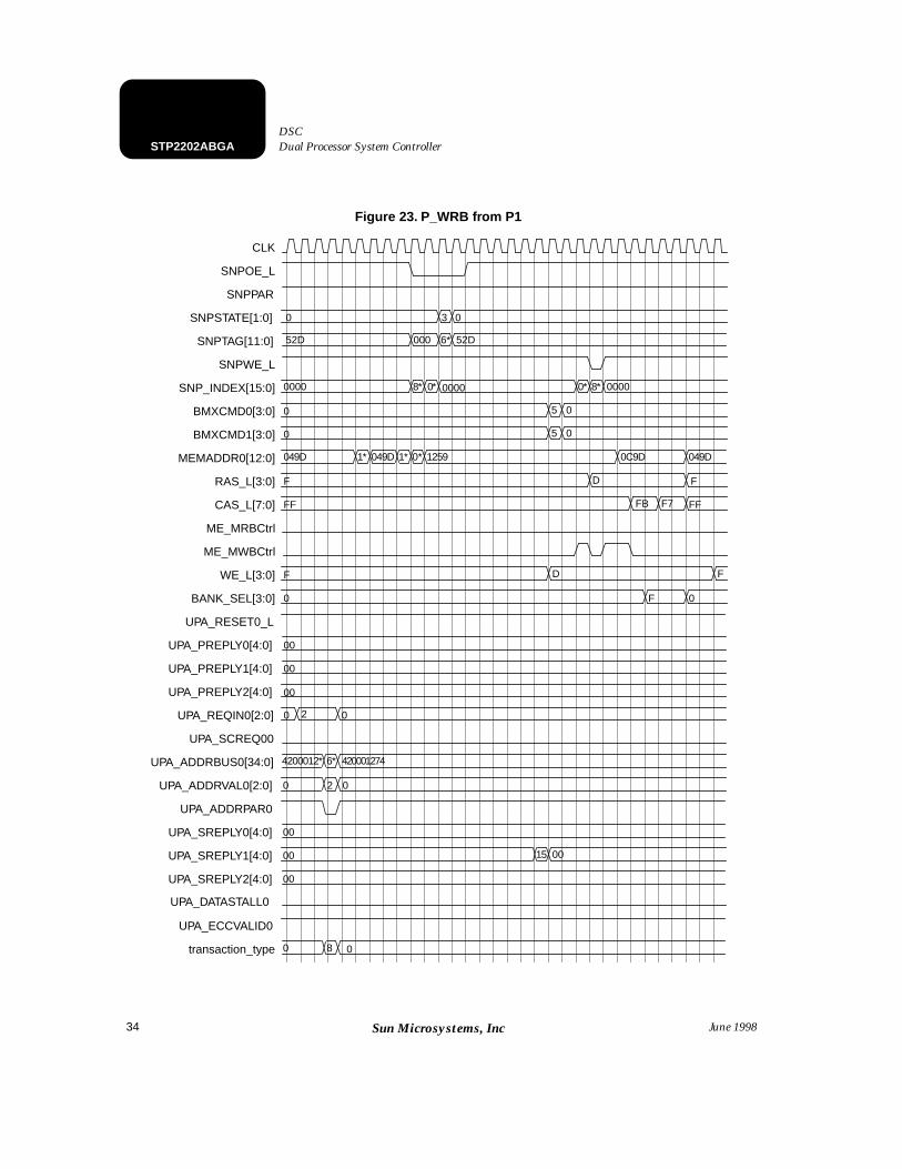
Figure 23. P_WRB from P1
8*
0
52D
CLK
SNPOE_L
SNPPAR
SNPSTATE[1:0]
SNPTAG[11:0]
SNPWE_L
SNP_INDEX[15:0] 0*
BMXCMD0[3:0] 0
BMXCMD1[3:0]
MEMADDR0[12:0] 049D1259049D
RAS_L[3:0] F
CAS_L[7:0] FF
ME_MRBCtrl
ME_MWBCtrl
WE_L[3:0] F
BANK_SEL[3:0]
UPA_RESET0_L
UPA_PREPLY0[4:0] 00
UPA_PREPLY1[4:0] 00
UPA_PREPLY2[4:0] 00
UPA_REQIN0[2:0] 02
UPA_SCREQ00
UPA_ADDRBUS0[34:0] 4200012746*
UPA_ADDRVAL0[2:0] 0 2
UPA_ADDRPAR0
UPA_SREPLY0[4:0] 00
UPA_SREPLY1[4:0] 00
UPA_SREPLY2[4:0] 00
UPA_DATASTALL0
UPA_ECCVALID0
transaction_type 80 0
0
4200012*
0
0
3 0
0000
0C9D
D F
F7 FF
F 0
0*8*0000 0000
1*
000 6* 52D
5 0
0 5 0
049D 1* 0*
FB
D F
15 00
35
Dual Processor System ControllerDSC
STP2202ABGA
June 1998 Sun Microsystems, Inc
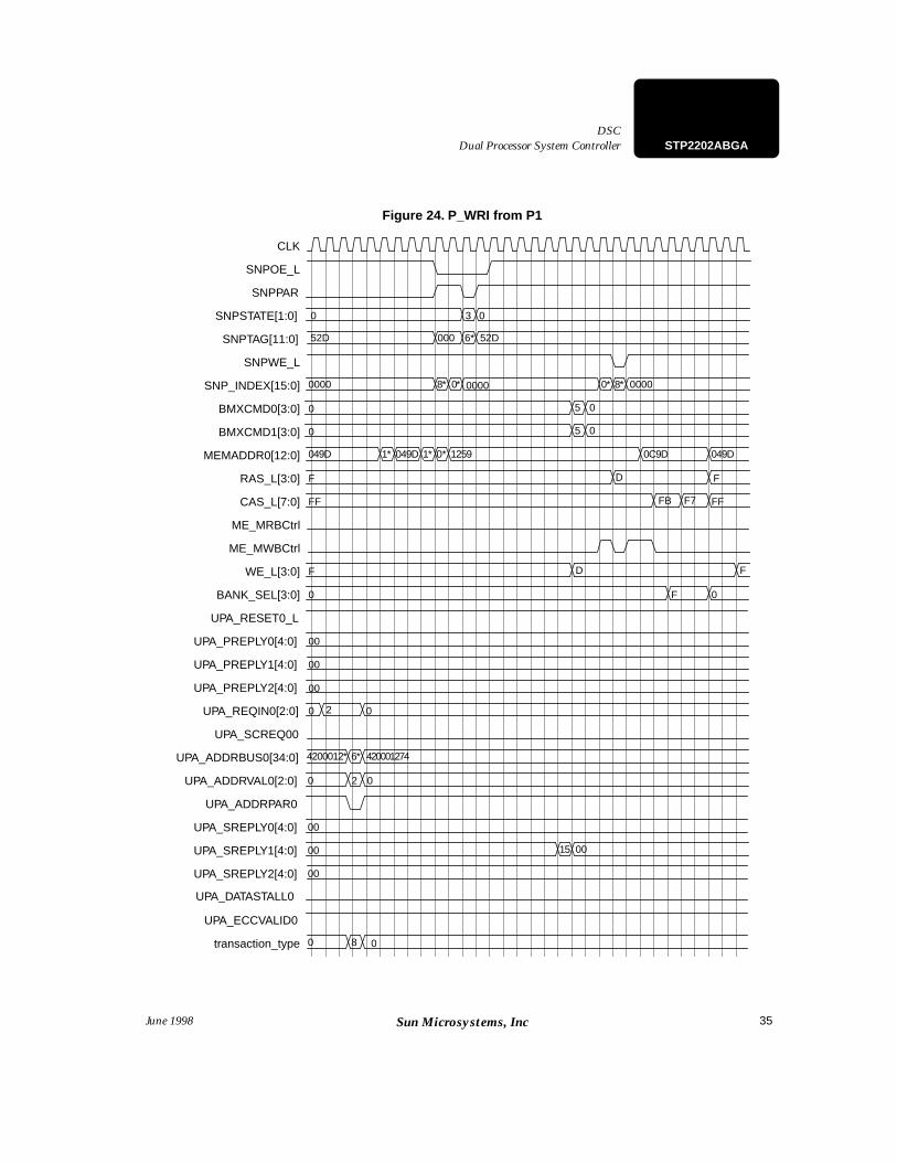
Figure 24. P_WRI from P1
8*
0
52D
CLK
SNPOE_L
SNPPAR
SNPSTATE[1:0]
SNPTAG[11:0]
SNPWE_L
SNP_INDEX[15:0] 0*
BMXCMD0[3:0] 0
BMXCMD1[3:0]
MEMADDR0[12:0] 049D1259049D
RAS_L[3:0] F
CAS_L[7:0] FF
ME_MRBCtrl
ME_MWBCtrl
WE_L[3:0] F
BANK_SEL[3:0]
UPA_RESET0_L
UPA_PREPLY0[4:0] 00
UPA_PREPLY1[4:0] 00
UPA_PREPLY2[4:0] 00
UPA_REQIN0[2:0] 02
UPA_SCREQ00
UPA_ADDRBUS0[34:0] 4200012746*
UPA_ADDRVAL0[2:0] 0 2
UPA_ADDRPAR0
UPA_SREPLY0[4:0] 00
UPA_SREPLY1[4:0] 00
UPA_SREPLY2[4:0] 00
UPA_DATASTALL0
UPA_ECCVALID0
transaction_type 80 0
0
4200012*
0
0
3 0
0000
0C9D
D F
F7 FF
F 0
0*8*0000 0000
1*
000 6* 52D
5 0
0 5 0
049D 1* 0*
FB
D F
15 00
36
STP2202ABGA Dual Processor System Controller DSC
June 1998Sun Microsystems, Inc
Basic Memory Timing
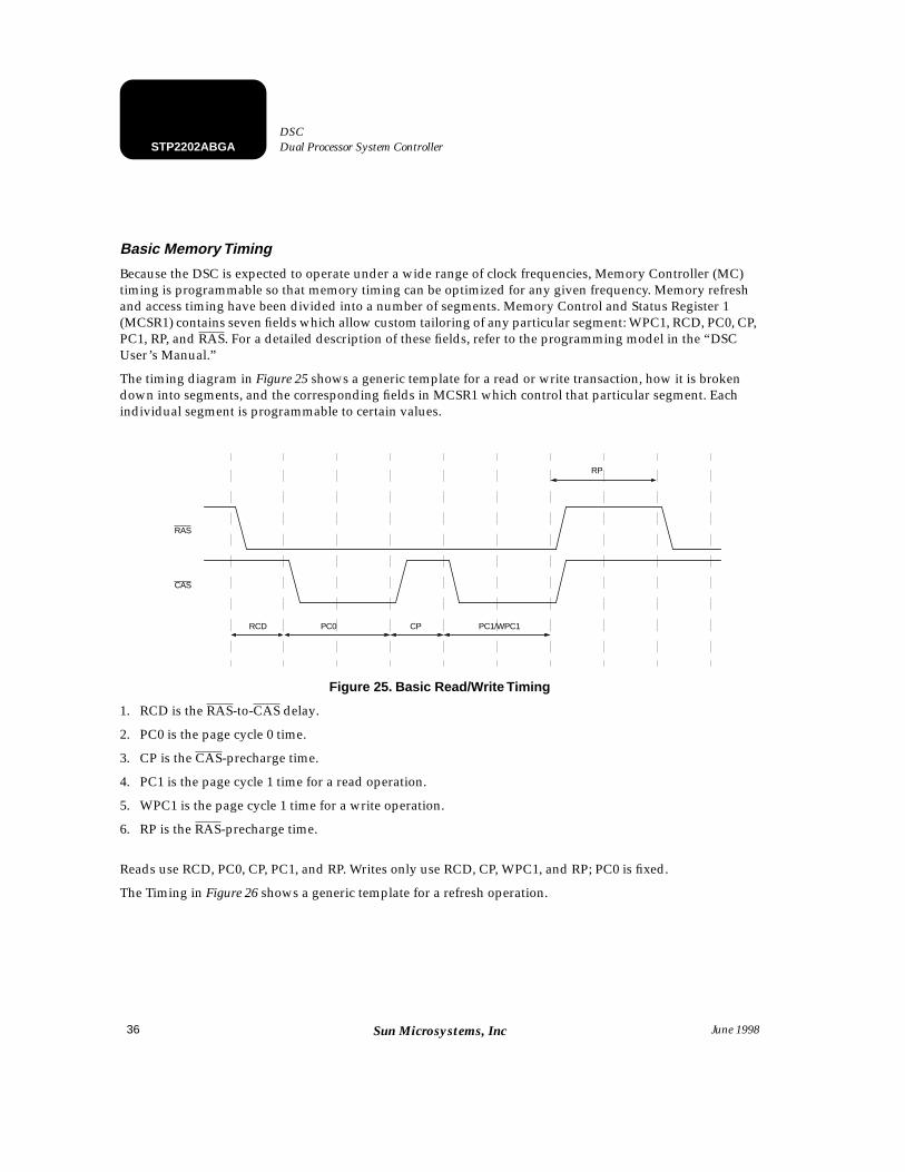
Because the DSC is expected to operate under a wide range of clock frequencies, Memory Controller (MC) timing is programmable so that memory timing can be optimized for any given frequency. Memory refresh and access timing have been divided into a number of segments. Memory Control and Status Register 1 (MCSR1) contains seven fields which allow custom tailoring of any particular segment: WPC1, RCD, PC0, CP, PC1, RP, and RAS. For a detailed description of these fields, refer to the programming model in the “DSC User’s Manual.”
The timing diagram in Figure 25 shows a generic template for a read or write transaction, how it is broken down into segments, and the corresponding fields in MCSR1 which control that particular segment. Each individual segment is programmable to certain values.
Figure 25. Basic Read/Write Timing
1. RCD is the RAS-to-CAS delay.
2. PC0 is the page cycle 0 time.
3. CP is the CAS-precharge time.
4. PC1 is the page cycle 1 time for a read operation.
5. WPC1 is the page cycle 1 time for a write operation.
6. RP is the RAS-precharge time.
Reads use RCD, PC0, CP, PC1, and RP. Writes only use RCD, CP, WPC1, and RP; PC0 is fixed.
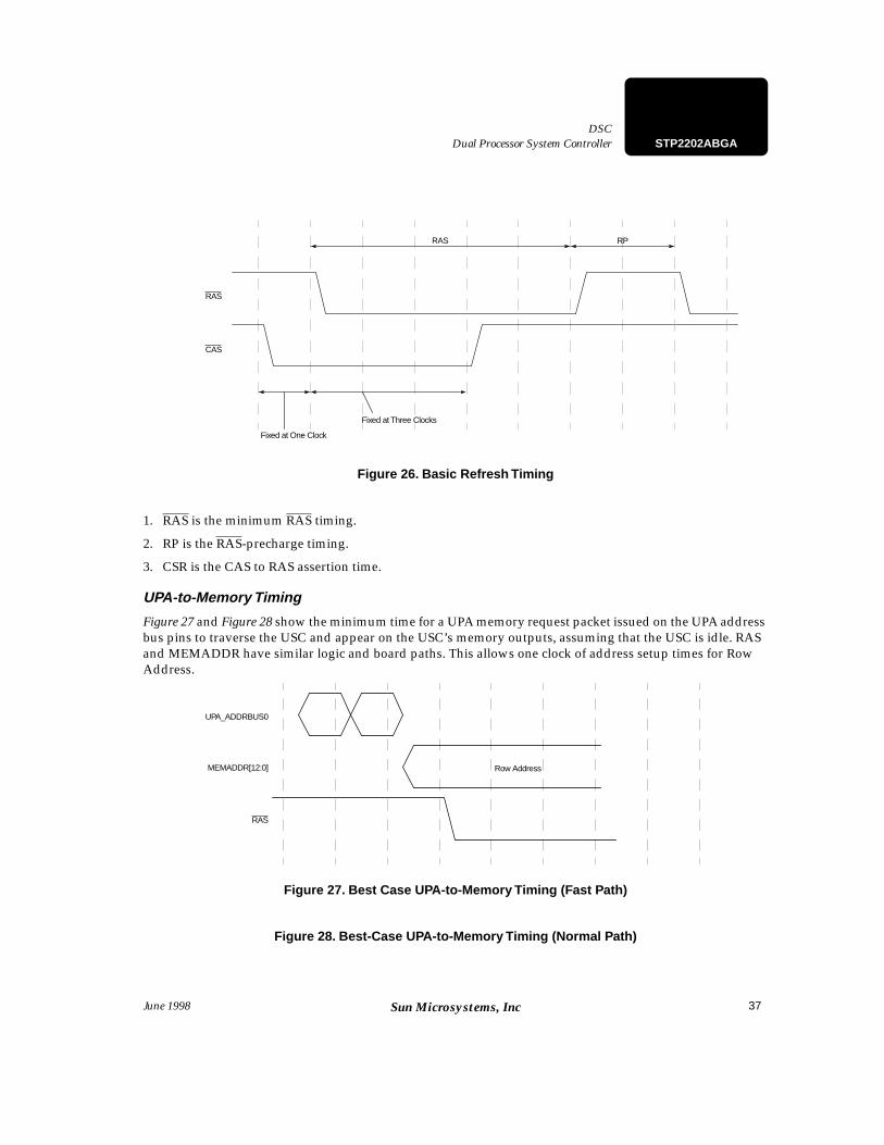
The Timing in Figure 26 shows a generic template for a refresh operation.
RAS
CAS
RCD PC0 CP PC1/WPC1
RP
37
Dual Processor System ControllerDSC
STP2202ABGA
June 1998 Sun Microsystems, Inc
Figure 26. Basic Refresh Timing
1. RAS is the minimum RAS timing.
2. RP is the RAS-precharge timing.
3. CSR is the CAS to RAS assertion time.
UPA-to-Memory Timing
Figure 27 and Figure 28 show the minimum time for a UPA memory request packet issued on the UPA address bus pins to traverse the USC and appear on the USC’s memory outputs, assuming that the USC is idle. RAS and MEMADDR have similar logic and board paths. This allows one clock of address setup times for Row Address.
Figure 27. Best Case UPA-to-Memory Timing (Fast Path)
Figure 28. Best-Case UPA-to-Memory Timing (Normal Path)
RAS
CAS
RPRAS
Fixed at Three Clocks
Fixed at One Clock
UPA_ADDRBUS0
MEMADDR[12:0]
RAS
Row Address
38
STP2202ABGA Dual Processor System Controller DSC
June 1998Sun Microsystems, Inc
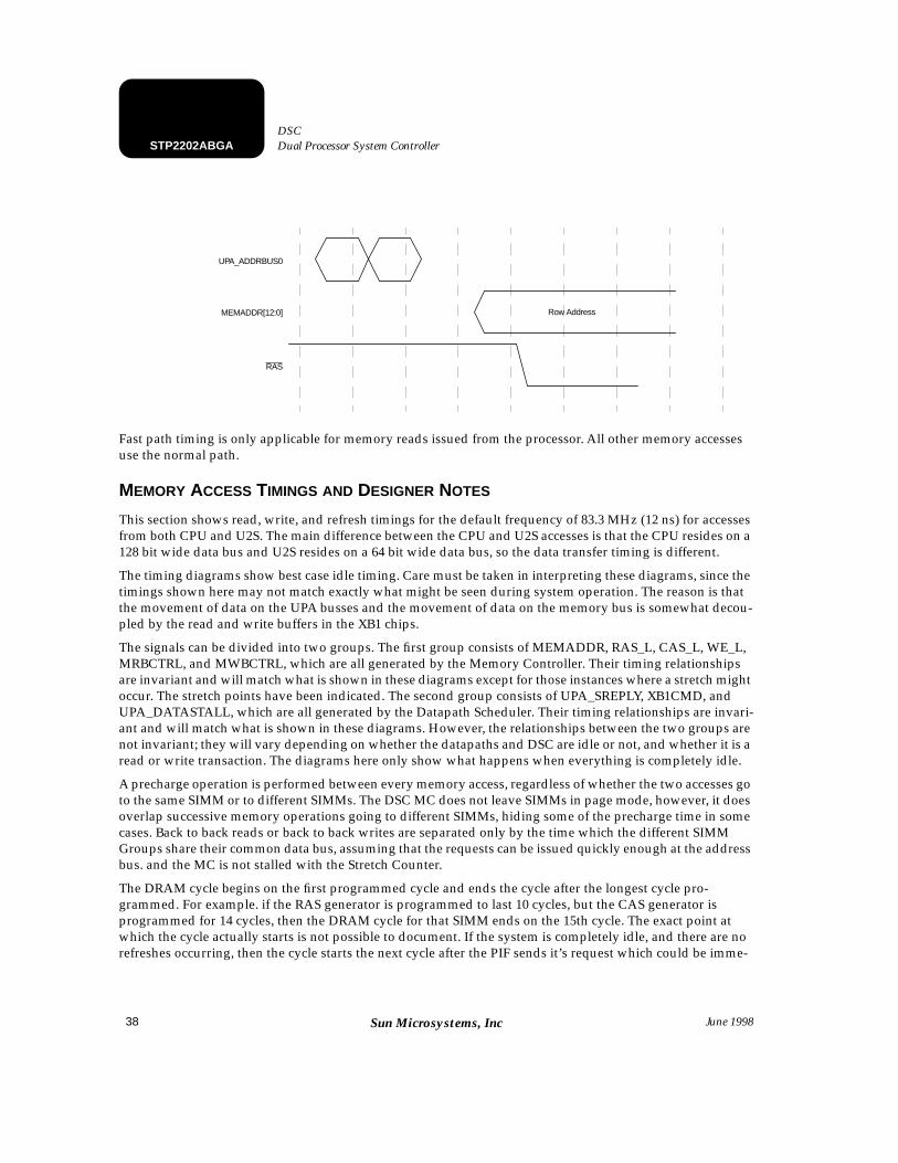
Fast path timing is only applicable for memory reads issued from the processor. All other memory accesses use the normal path.
MEMORY ACCESS TIMINGS AND DESIGNER NOTES
This section shows read, write, and refresh timings for the default frequency of 83.3 MHz (12 ns) for accesses from both CPU and U2S. The main difference between the CPU and U2S accesses is that the CPU resides on a 128 bit wide data bus and U2S resides on a 64 bit wide data bus, so the data transfer timing is different.
The timing diagrams show best case idle timing. Care must be taken in interpreting these diagrams, since the timings shown here may not match exactly what might be seen during system operation. The reason is that the movement of data on the UPA busses and the movement of data on the memory bus is somewhat decou-pled by the read and write buffers in the XB1 chips.
The signals can be divided into two groups. The first group consists of MEMADDR, RAS_L, CAS_L, WE_L, MRBCTRL, and MWBCTRL, which are all generated by the Memory Controller. Their timing relationships are invariant and will match what is shown in these diagrams except for those instances where a stretch might occur. The stretch points have been indicated. The second group consists of UPA_SREPLY, XB1CMD, and UPA_DATASTALL, which are all generated by the Datapath Scheduler. Their timing relationships are invari-ant and will match what is shown in these diagrams. However, the relationships between the two groups are not invariant; they will vary depending on whether the datapaths and DSC are idle or not, and whether it is a read or write transaction. The diagrams here only show what happens when everything is completely idle.
A precharge operation is performed between every memory access, regardless of whether the two accesses go to the same SIMM or to different SIMMs. The DSC MC does not leave SIMMs in page mode, however, it does overlap successive memory operations going to different SIMMs, hiding some of the precharge time in some cases. Back to back reads or back to back writes are separated only by the time which the different SIMM Groups share their common data bus, assuming that the requests can be issued quickly enough at the address bus. and the MC is not stalled with the Stretch Counter.
The DRAM cycle begins on the first programmed cycle and ends the cycle after the longest cycle pro-grammed. For example. if the RAS generator is programmed to last 10 cycles, but the CAS generator is programmed for 14 cycles, then the DRAM cycle for that SIMM ends on the 15th cycle. The exact point at which the cycle actually starts is not possible to document. If the system is completely idle, and there are no refreshes occurring, then the cycle starts the next cycle after the PIF sends it’s request which could be imme-
UPA_ADDRBUS0
MEMADDR[12:0]
RAS
Row Address
39
Dual Processor System ControllerDSC
STP2202ABGA
June 1998 Sun Microsystems, Inc
diately after the UPA request or not. If there is a refresh occurring, then the refresh must finish before the request starts. If there are other transactions in progress, then there may be some dependencies as to when the operation can start depending on whether the request is for the same group of SIMMs or if the request is for a different group of SIMMs.
A question arises as to when cycles actually start and end. This is not an easy question to answer if you can only look at UPA transactions and DRAM array outputs. If you use the debug pins and output the internal Start signal in the MC then that defines the actual beginning of a cycle, but there is no reasonable way to doc-ument all the possibilities of when the DRAM cycle starts by only observing the UPA requests and DRAM outputs.
Another question arises as to how cancelled reads affect DRAM timing. They really do not affect reads. In the case of a cancel (due to the cc deciding to provide the data from the other processor’s cache) the read from memory continues and is simply not used. The case seen in the lab, where the timing appeared to be a func-tion of cancels was a bug which should be corrected as of this writing.
Notes on the following timing diagrams regarding stretch points, ping pong points and timer information.
1. The address must be asserted until cycle 5. As described in Chapter 4, Programming Model Section 4.3.5, “Memory Controller Registers,” on page 4-45 of the DSC User’s manual. The correct value to program PPRdCnt would be 5 - 2 = 3 for this behavior.
2. StretchRd: As described in Section 4.3.5, “Memory Controller Registers,” on page 4-45, there are five cycles before MRB_Ctrl needs to pulse, therefore the correct stretch point is just before the first pulse. The value which StretchRd needs to be programmed to is 5 - 2 = 3.
3. Regarding the timer values: As an example, we will look at SameBusyRdRd. This value specifies the earliest time at which the next read to the same group of SIMMs can start. All these values depend on the specifics of the system clock speed, the DRAM timing information, and the specific way the waveforms are programmed. There is an initial cycle at the beginning of the read (which the subsequent read to the same SIMM will also have). The system clock speed is 12 ns per cycle. The DRAMs are standard 60 ns DRAMs. Therefore tRAS is 60 ns, tRP is 40 ns, and tRC is 110 ns. We have 5 cycles where RAS is low thus satisfying tRAS, we could have RAS high for 4 cycles giving us 48 ns, thus satisfying tRP, but then tRC is only 108 ns. Therefore, tRP also needs to be 5 cycles. This means that the earliest the next cycle to the same group can begin is in 10 cycles. As described in Section 4.3.5, “Memory Controller Registers,” on page 4-45, we subtract two from this and get 8. SameBusy RdRd needs to be programmed to 8 for the tightest allowable read to read spacing to the same group. When looking at timer values for different groups, the worst case timing for the address bus and data bus must be accounted for, to get the tightest spacing for those.
SIMULATED MC TIMING EXAMPLES AND NOTES
This section contains a set of examples that shows both internal and external waveforms. These samples are extracted from the simulation tool and are used for illustration only. By reviewing the CSR values, the timing diagrams, and the descriptions, it is hoped that a better understanding of the MC will be obtained.
40
STP2202ABGA Dual Processor System Controller DSC
June 1998Sun Microsystems, Inc
A non-optimized set of Memory CSR’s that work with the simulation environment is shown below. The clock in this case is 50 MHz (20ns).
These CSR values were used when generating the following waveforms.
Writes to Different Groups
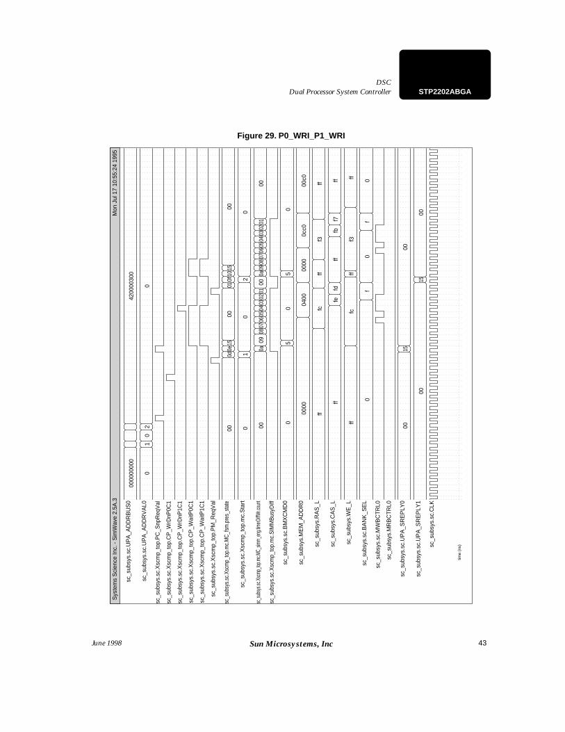
Figure 29 Illustrates two consecutive writes going to two different groups from different CPUs. The general sequence is as follows:
1. The PM_ReqVal signal starts the MC FSM.
2. The mc_fsm sends out the start signal to Group 0 generators on the next clock.
3. The DPS tell the CPU to write to the XB1 write buffers on the next clock.
4. The Timers start counting.
5. The DPS tells the XB1 to accept the Write Data on the next clock.
6. WE_L is activated and remains so throughout the write cycle.
7. Another PM_ReqVal signal arrives, requesting group 1. Since SIMMBusyDiff is active, the next Write cannot be started and the FSM goes into a Pending state.
8. SIMMBusyDiff is inactive on the next clock cycle and the start to group 1 is initiated.
9. And so on...
It may be possible to eliminate the “Pending” cycle by reducing the Diff_Busy_Wr_Wr count from a to 9 if the memory address hold time does not get violated in the process. The memory address appears to be the limit-ing factor in this case. Note that the DiffWr counter is held for one cycle in state 09. This is because the DM_WBAck signal has not yet arrived and the state machines are held. See also Figure 35.
TABLE 1: CSR values for timing examples
Address Value (Hex) Function
80 a0c10f18 Mem_Control0
84 263725b3 RAS_Control
88 00004da3 CAS_RD_Control
8c 29362692 BankSel_Control
90 2c98249a XB1_Buffer_Control
94 24cb24c7 CAS_WR_Control
98 14ac0279 Phase_Level_Control
9c 02952549 SIMM_Busy_Rd_Control
a0 06020543 Count_Control
a4 249324b7 Refresh_Control
a8 29b52493 Row_Control
b0 14952549 SIMM_Busy_Wr_Control
b4 12952549 SIMM_Busy_Refr_Control
41
Dual Processor System ControllerDSC
STP2202ABGA
June 1998 Sun Microsystems, Inc
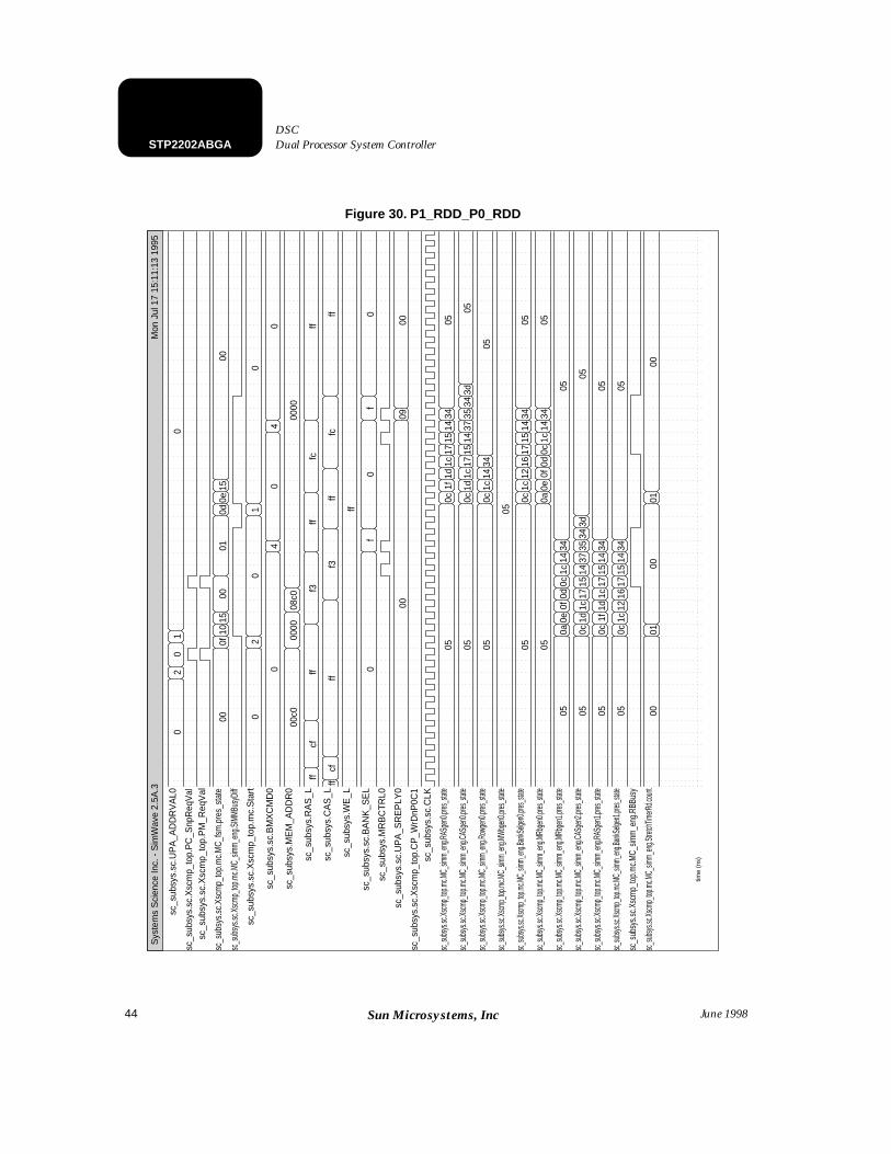
Reads to Different Groups
Figure 30 shows consecutive reads from two groups from CPU 1 and then CPU 0. There appears to be some optimization that can be made here with the Diff_Busy_RD_RD counter. The limiting factors include the Memory Address and the RB_Busy signal. It may be necessary to move out the StretchTimerRd by two cycles so that the MC samples RB_Busy at a more appropriate time. Right before you need to start filling the XB1 buffer is the suggested time. This would be a cycle before the internal mrb_ctrl signals are activated. It appears that the Diff_Busy _RD_RD counter could be reduced by as many as 5 cycles if the StretchTimer Rd is increased by 2 cycles.
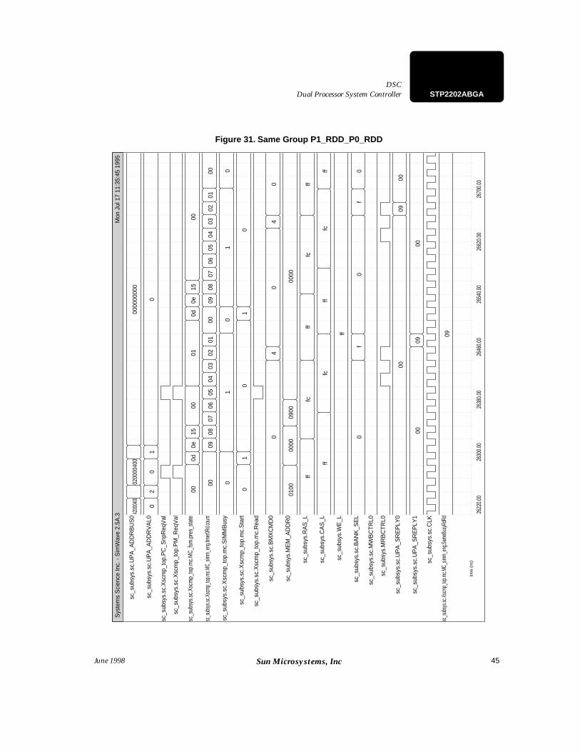
Reads to the Same Group
Figure 31 shows consecutive reads to the same SIMM group. The CAS generator is currently taking 10 cycles. Since it must be in idle before accepting another start signal, only be reducing the CAS generator state machine sequence can we reduce the SIMMBusy count. Since the cycle count in the last phase of CAS_RD is 2, the state machine effectively cycles for 2 counts during that stage. Reducing the last phase to 1 will have no effect on the waveform, yet will let the state machine go to the idle state 1 cycle earlier. Hence, a start pulse can be received 1 cycle earlier.
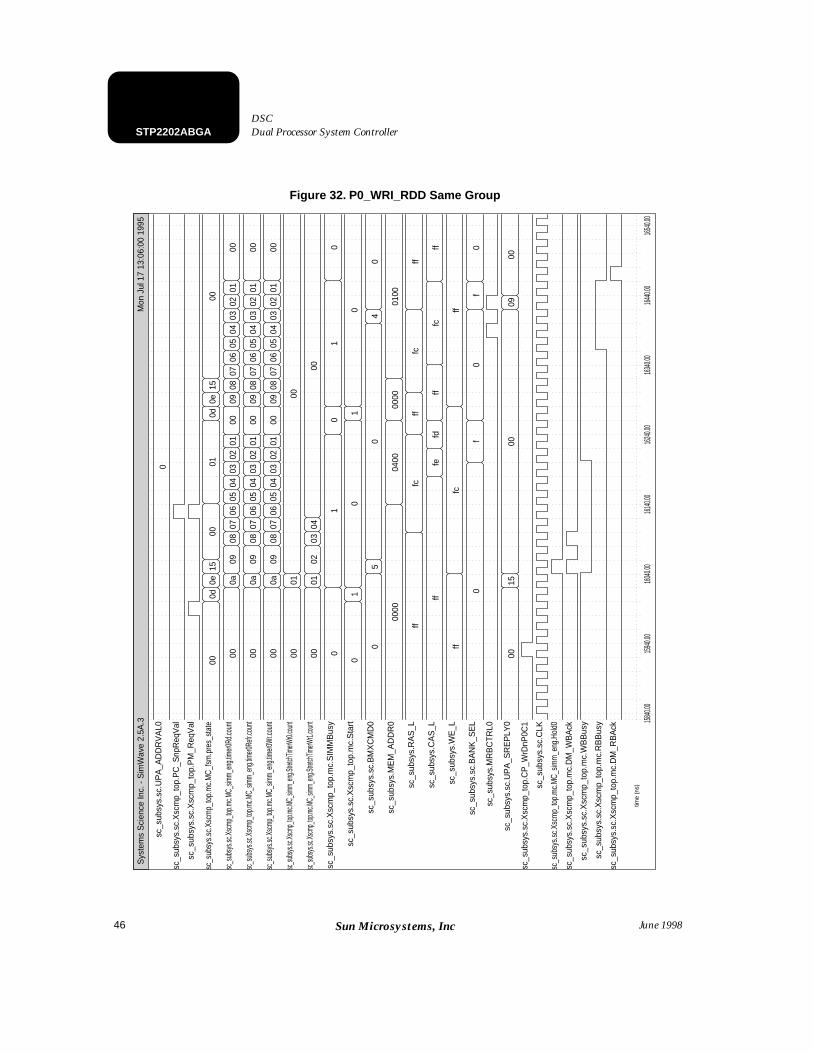
Write followed by a read
In this example, shown in Figure 32, a write is followed by a read in the same group. This example shows the internal Hold0 signal, which keeps the cycles in the timer “timer0Wr” from decrementing. This hold signal is the result of WB_Busy being active when the StretchTimerWr0 counter has expired and polls WB_Busy to see if the XB1 buffer has acquired it’s data. The next cycle, XB1 has acquired the data, the DPS sends DM_WBAck and the WB_Busy goes inactive and allows the timer0Wr counter to proceed.
The limiting factor in starting the Read in this case is the rising edge of CAS. It does not appear that any addi-tional cycles can be gained from this sequence.
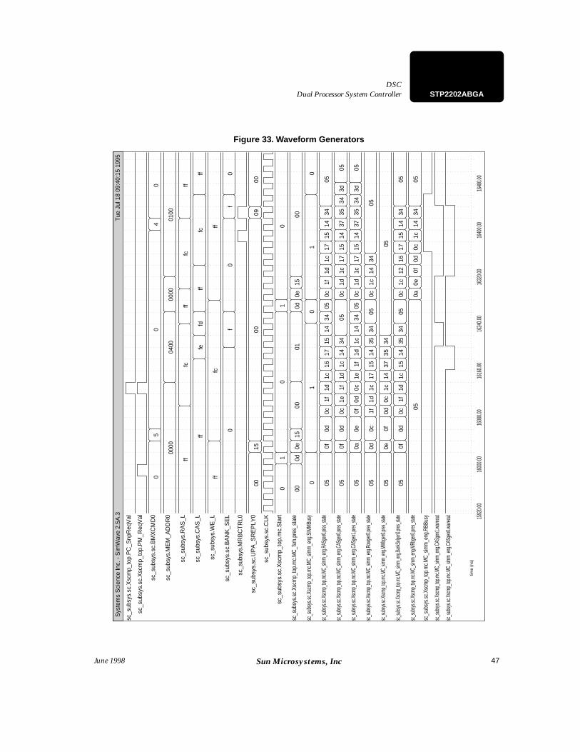
Waveform generators
Figure 33. shows various waveform generator state machine sequences for both a write and a read.
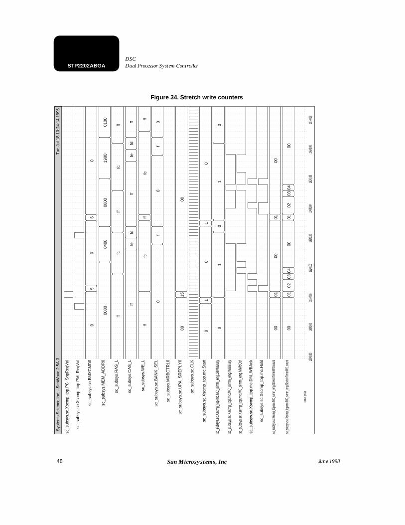
Stretch Write counters
Figure 34. shows the stretch write counters. It a sequence of two writes, one from CPU1 and the next from U2S. When the stretch write counters expire, they check the WB_Busy signal to see if the XB1 buffer is loaded. From the figure, we can see that the CPU data is loaded very quickly and there is only 1 hold state before the both SIMM pairs can be written. However, the second write is from U2S and the waveform generators are held for both the first and second datums. The important thing to watch for is that the StretchWr1 must be long enough so that it samples WB_Busy after the second DM_WBAck arrives. If StretchWr1 is too small, it will sample WB_Busy during after the first DM_WBAck and think that data has arrived and inappropriately write the data to memory. Thankfully, the DPS block will always place DM_WBAck 4 cycles apart on Writes from U2S and the StrechWr1 counter is held when the hold signal is active.
For performance, it’s best to minimize the StretchWr counters.
42
STP2202ABGA Dual Processor System Controller DSC
June 1998Sun Microsystems, Inc
Ping-Pong buffers
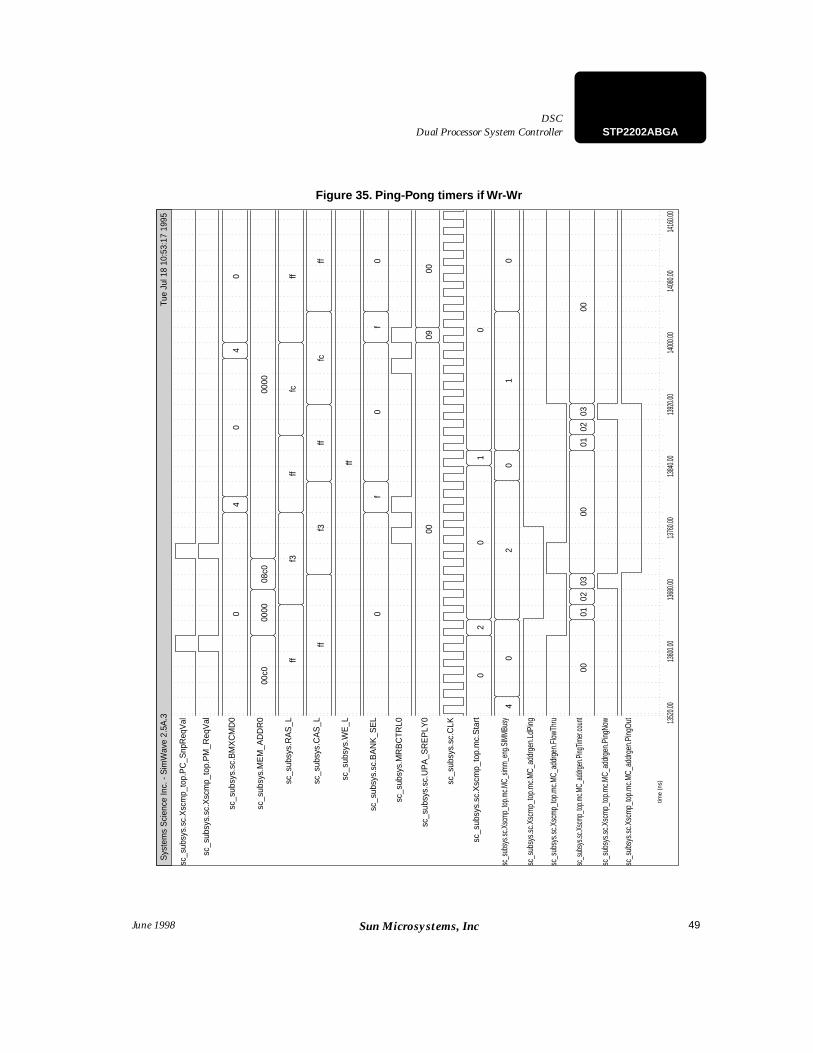
Figure 35. shows the ping-pong buffers on 2 consecutive reads. When the PP timer expires it sends out the PingNow signal. That, in turn, causes the memory addresses to be originated from the other buffer. For per-formance optimization, you want the next address to appear as soon as it can while not causing address hold time violations for the current operation.
43
Dual Processor System ControllerDSC
STP2202ABGA
June 1998 Sun Microsystems, Inc
Figure 29. P0_WRI_P1_WRI
Sys
tem
s S
cien
ce In
c. -
Sim
Wav
e 2.
5A.3
Mon
Jul
17
10:5
5:24
199
5
time
(ns)
sc_s
ubsy
s.sc
.UP
A_A
DD
RB
US
0
sc_s
ubsy
s.sc
.UP
A_A
DD
RV
AL0
sc_s
ubsy
s.sc
.Xsc
mp_
top.
PC
_Snp
Req
Val
sc_s
ubsy
s.sc
.Xsc
mp_
top.
CP
_WrD
nP0C
1
sc_s
ubsy
s.sc
.Xsc
mp_
top.
CP
_WrD
nP1C
1
sc_s
ubsy
s.sc
.Xsc
mp_
top.
CP
_Wai
tP0C
1
sc_s
ubsy
s.sc
.Xsc
mp_
top.
CP
_Wai
tP1C
1
sc_s
ubsy
s.sc
.Xsc
mp_
top.
PM
_Req
Val
sc_s
ubsy
s.sc
.Xsc
mp_
top.
mc.
MC_
fsm
.pre
s_st
ate
sc_s
ubsy
s.sc
.Xsc
mp_
top.
mc.
Sta
rt
sc_s
ubsy
s.sc.X
scmp
_top.m
c.MC_
simm_
eng.t
imerD
iffWr.c
ount
sc_s
ubsy
s.sc
.Xsc
mp_
top.
mc.
SIM
MB
usyD
iff
sc_s
ubsy
s.sc
.BM
XC
MD
0
sc_s
ubsy
s.M
EM
_AD
DR
0
sc_s
ubsy
s.R
AS
_L
sc_s
ubsy
s.C
AS
_L
sc_s
ubsy
s.W
E_L
sc_s
ubsy
s.sc
.BA
NK
_SE
L
sc_s
ubsy
s.sc
.MW
BC
TRL0
sc_s
ubsy
s.M
RB
CTR
L0
sc_s
ubsy
s.sc
.UP
A_S
RE
PLY
0
sc_s
ubsy
s.sc
.UP
A_S
RE
PLY
1
sc_s
ubsy
s.sc
.CLK
0000
0000
042
0000
300
01
02
0
000d
0e15
0001
0f10
1500
01
02
0
000a
0908
0706
0504
0302
0100
0a09
0807
0605
0403
0201
00
05
05
0
0000
0400
0000
0cc0
00c0
fffc
fff3
ff
fffe
fdff
fbf7
ff
fffc
fff3
ff
0f
0f
0
0015
00
0015
00
44
STP2202ABGA Dual Processor System Controller DSC
June 1998Sun Microsystems, Inc
Figure 30. P1_RDD_P0_RDD
Sys
tem
s S
cien
ce In
c. -
Sim
Wav
e 2.
5A.3
Mon
Jul
17
15:1
1:13
199
5
time
(ns)
sc_s
ubsy
s.sc
.UP
A_A
DD
RV
AL0
sc_s
ubsy
s.sc
.Xsc
mp_
top.
PC
_Snp
Req
Val
sc_s
ubsy
s.sc
.Xsc
mp_
top.
PM
_Req
Val
sc_s
ubsy
s.sc
.Xsc
mp_
top.
mc.
MC_
fsm
.pre
s_st
ate
sc_s
ubsy
s.sc.X
scmp
_top.m
c.MC_
simm_
eng.S
IMMB
usyD
iff
sc_s
ubsy
s.sc
.Xsc
mp_
top.
mc.
Sta
rt
sc_s
ubsy
s.sc
.BM
XC
MD
0
sc_s
ubsy
s.M
EM
_AD
DR
0
sc_s
ubsy
s.R
AS
_L
sc_s
ubsy
s.C
AS
_L
sc_s
ubsy
s.W
E_L
sc_s
ubsy
s.sc
.BA
NK
_SE
L
sc_s
ubsy
s.M
RB
CTR
L0
sc_s
ubsy
s.sc
.UP
A_S
RE
PLY
0
sc_s
ubsy
s.sc
.Xsc
mp_
top.
CP
_WrD
nP0C
1sc
_sub
sys.
sc.C
LK
sc_s
ubsy
s.sc.X
scmp
_top.m
c.MC_
simm_
eng.R
ASge
n0.pr
es_s
tate
sc_s
ubsy
s.sc.X
scmp
_top.m
c.MC_
simm_
eng.C
ASge
n0.pr
es_s
tate
sc_s
ubsy
s.sc.X
scmp
_top.m
c.MC_
simm_
eng.R
owge
n0.pr
es_s
tate
sc_su
bsys.
sc.Xs
cmp_
top.m
c.MC_
simm_
eng.M
Wbge
n0.pr
es_s
tate
sc_su
bsys.
sc.Xs
cmp_
top.m
c.MC_
simm_
eng.B
ankS
elgen
0.pres
_stat
e
sc_s
ubsy
s.sc.X
scmp
_top.m
c.MC_
simm_
eng.M
Rbge
n0.pr
es_s
tate
sc_s
ubsy
s.sc.X
scmp
_top.m
c.MC_
simm_
eng.M
Rbge
n1.pr
es_s
tate
sc_s
ubsy
s.sc.X
scmp
_top.m
c.MC_
simm_
eng.C
ASge
n2.pr
es_s
tate
sc_s
ubsy
s.sc.X
scmp
_top.m
c.MC_
simm_
eng.R
ASge
n1.pr
es_s
tate
sc_su
bsys.
sc.Xs
cmp_
top.m
c.MC_
simm_
eng.B
ankS
elgen
1.pres
_stat
e
sc_s
ubsy
s.sc.X
scm
p_to
p.m
c.MC_
simm
_eng
.RBB
usy
sc_su
bsys.
sc.Xs
cmp_
top.m
c.MC_
simm_
eng.S
tretch
TimerR
d.cou
nt
02
01
0
000f
1015
0001
0d0e
1500
02
01
0
04
04
0
00c0
0000
08c0
0000
ffcf
fff3
fffc
ff
ffcf
fff3
fffc
ff
ff
0f
0f
0
0009
00
050c
1f1d
1c17
1514
3405
050c
1d1c
1715
1437
3534
3d05
050c
1c14
3405
05
050c
1c12
1617
1514
3405
050a
0e0f
0d0c
1c14
3405
050a
0e0f
0d0c
1c14
3405
050c
1d1c
1715
1437
3534
3d05
050c
1f1d
1c17
1514
3405
050c
1c12
1617
1514
3405
0001
0001
00
45
Dual Processor System ControllerDSC
STP2202ABGA
June 1998 Sun Microsystems, Inc
Figure 31. Same Group P1_RDD_P0_RDD
Sys
tem
s S
cien
ce In
c. -
Sim
Wav
e 2.
5A.3
Mon
Jul
17
11:3
5:45
199
5
time
(ns)
2622
0.00
2630
0.00
2638
0.00
2646
0.00
2654
0.00
2662
0.00
2670
0.00
sc_s
ubsy
s.sc
.UP
A_A
DD
RB
US
0
sc_s
ubsy
s.sc
.UP
A_A
DD
RV
AL0
sc_s
ubsy
s.sc
.Xsc
mp_
top.
PC
_Snp
Req
Val
sc_s
ubsy
s.sc
.Xsc
mp_
top.
PM
_Req
Val
sc_s
ubsy
s.sc
.Xsc
mp_
top.
mc.
MC_
fsm
.pre
s_st
ate
sc_s
ubsy
s.sc.X
scmp
_top.m
c.MC_
simm_
eng.t
imer0
Rd.co
unt
sc_s
ubsy
s.sc
.Xsc
mp_
top.
mc.
SIM
MB
usy
sc_s
ubsy
s.sc
.Xsc
mp_
top.
mc.
Sta
rt
sc_s
ubsy
s.sc
.Xsc
mp_
top.
mc.
Rea
d
sc_s
ubsy
s.sc
.BM
XC
MD
0
sc_s
ubsy
s.M
EM
_AD
DR
0
sc_s
ubsy
s.R
AS
_L
sc_s
ubsy
s.C
AS
_L
sc_s
ubsy
s.W
E_L
sc_s
ubsy
s.sc
.BA
NK
_SE
L
sc_s
ubsy
s.sc
.MW
BC
TRL0
sc_s
ubsy
s.M
RB
CTR
L0
sc_s
ubsy
s.sc
.UP
A_S
RE
PLY
0
sc_s
ubsy
s.sc
.UP
A_S
RE
PLY
1
sc_s
ubsy
s.sc
.CLK
sc_s
ubsy
s.sc.X
scmp
_top.m
c.MC_
simm_
eng.S
ameB
usyR
dRd
420000
40002
0000
400
0000
0000
0
02
01
0
000d
0e15
0001
0d0e
1500
0009
0807
0605
0403
0201
0009
0807
0605
0403
0201
00
01
01
0
01
01
0
04
04
0
0100
0000
0900
0000
fffc
fffc
ff
fffc
fffc
ff
ff
0f
0f
0
0009
00
0009
00
09
46
STP2202ABGA Dual Processor System Controller DSC
June 1998Sun Microsystems, Inc
Figure 32. P0_WRI_RDD Same Group
Sys
tem
s S
cien
ce In
c. -
Sim
Wav
e 2.
5A.3
Mon
Jul
17
13:0
6:00
199
5
time
(ns)
1584
0.00
1594
0.00
1604
0.00
1614
0.00
1624
0.00
1634
0.00
1644
0.00
1654
0.00
sc_s
ubsy
s.sc
.UP
A_A
DD
RV
AL0
sc_s
ubsy
s.sc
.Xsc
mp_
top.
PC
_Snp
Req
Val
sc_s
ubsy
s.sc
.Xsc
mp_
top.
PM
_Req
Val
sc_s
ubsy
s.sc
.Xsc
mp_
top.
mc.
MC_
fsm
.pre
s_st
ate
sc_s
ubsy
s.sc.X
scmp
_top.m
c.MC_
simm_
eng.t
imer0
Rd.co
unt
sc_s
ubsy
s.sc.X
scmp
_top.m
c.MC_
simm_
eng.t
imer0
Refr.c
ount
sc_s
ubsy
s.sc.X
scmp
_top.m
c.MC_
simm_
eng.t
imer0
Wr.c
ount
sc_su
bsys.
sc.Xs
cmp_
top.m
c.MC_
simm_
eng.S
tretch
TimerW
r0.co
unt
sc_su
bsys.
sc.Xs
cmp_
top.m
c.MC_
simm_
eng.S
tretch
TimerW
r1.co
unt
sc_s
ubsy
s.sc
.Xsc
mp_
top.
mc.
SIM
MB
usy
sc_s
ubsy
s.sc
.Xsc
mp_
top.
mc.
Sta
rt
sc_s
ubsy
s.sc
.BM
XC
MD
0
sc_s
ubsy
s.M
EM
_AD
DR
0
sc_s
ubsy
s.R
AS
_L
sc_s
ubsy
s.C
AS
_L
sc_s
ubsy
s.W
E_L
sc_s
ubsy
s.sc
.BA
NK
_SE
L
sc_s
ubsy
s.M
RB
CTR
L0
sc_s
ubsy
s.sc
.UP
A_S
RE
PLY
0
sc_s
ubsy
s.sc
.Xsc
mp_
top.
CP
_WrD
nP0C
1
sc_s
ubsy
s.sc
.CLK
sc_s
ubsy
s.sc
.Xsc
mp_
top.
mc.
MC_
simm
_eng
.Hol
d0
sc_s
ubsy
s.sc
.Xsc
mp_
top.
mc.
DM
_WB
Ack
sc_s
ubsy
s.sc
.Xsc
mp_
top.
mc.
WB
Bus
y
sc_s
ubsy
s.sc
.Xsc
mp_
top.
mc.
RB
Bus
y
sc_s
ubsy
s.sc
.Xsc
mp_
top.
mc.
DM
_RB
Ack
0
000d
0e15
0001
0d0e
1500
000a
0908
0706
0504
0302
0100
0908
0706
0504
0302
0100
000a
0908
0706
0504
0302
0100
0908
0706
0504
0302
0100
000a
0908
0706
0504
0302
0100
0908
0706
0504
0302
0100
0001
00
0001
0203
0400
01
01
0
01
01
0
05
04
0
0000
0400
0000
0100
fffc
fffc
ff
fffe
fdff
fcff
fffc
ff
0f
0f
0
0015
0009
00
47
Dual Processor System ControllerDSC
STP2202ABGA
June 1998 Sun Microsystems, Inc
Figure 33. Waveform Generators
Sys
tem
s S
cien
ce In
c. -
Sim
Wav
e 2.
5A.3
Tue
Jul 1
8 09
:40:
15 1
995
time
(ns)
1592
0.00
1600
0.00
1608
0.00
1616
0.00
1624
0.00
1632
0.00
1640
0.00
1648
0.00
sc_s
ubsy
s.sc
.Xsc
mp_
top.
PC
_Snp
Req
Val
sc_s
ubsy
s.sc
.Xsc
mp_
top.
PM
_Req
Val
sc_s
ubsy
s.sc
.BM
XC
MD
0
sc_s
ubsy
s.M
EM
_AD
DR
0
sc_s
ubsy
s.R
AS
_L
sc_s
ubsy
s.C
AS
_L
sc_s
ubsy
s.W
E_L
sc_s
ubsy
s.sc
.BA
NK
_SE
L
sc_s
ubsy
s.M
RB
CTR
L0
sc_s
ubsy
s.sc
.UP
A_S
RE
PLY
0
sc_s
ubsy
s.sc
.CLK
sc_s
ubsy
s.sc
.Xsc
mp_
top.
mc.
Sta
rt
sc_s
ubsy
s.sc
.Xsc
mp_
top.
mc.
MC_
fsm
.pre
s_st
ate
sc_s
ubsy
s.sc.X
scmp
_top.m
c.MC_
simm_
eng.S
IMMB
usy
sc_s
ubsy
s.sc.X
scmp
_top.m
c.MC_
simm_
eng.R
ASge
n0.pr
es_s
tate
sc_s
ubsy
s.sc.X
scmp
_top.m
c.MC_
simm_
eng.C
ASge
n0.pr
es_s
tate
sc_s
ubsy
s.sc.X
scmp
_top.m
c.MC_
simm_
eng.C
ASge
n1.pr
es_s
tate
sc_s
ubsy
s.sc.X
scmp
_top.m
c.MC_
simm_
eng.R
owge
n0.pr
es_s
tate
sc_su
bsys.
sc.Xs
cmp_
top.m
c.MC_
simm_
eng.M
Wbge
n0.pr
es_s
tate
sc_su
bsys.
sc.Xs
cmp_
top.m
c.MC_
simm_
eng.B
ankS
elgen
0.pres
_stat
e
sc_s
ubsy
s.sc.X
scmp
_top.m
c.MC_
simm_
eng.M
Rbge
n0.pr
es_s
tate
sc_s
ubsy
s.sc.X
scm
p_to
p.m
c.MC_
simm
_eng
.RBB
usy
sc_s
ubsy
s.sc.X
scmp
_top.m
c.MC_
simm_
eng.C
ASge
n1.w
aveo
ut
sc_s
ubsy
s.sc.X
scmp
_top.m
c.MC_
simm_
eng.C
ASge
n0.w
aveo
ut
05
04
0
0000
0400
0000
0100
fffc
fffc
ff
fffe
fdff
fcff
fffc
ff
0f
0f
0
0015
0009
00
01
01
0
000d
0e15
0001
0d0e
1500
01
01
0
050f
0d0c
1f1d
1c16
1715
1434
050c
1f1d
1c17
1514
3405
050f
0d0c
1e1f
1d1c
1434
050c
1d1c
1715
1437
3534
3d05
050a
0e0f
0d0c
1e1f
1d1c
1434
050c
1d1c
1715
1437
3534
3d05
050d
0c1f
1d1c
1715
1435
3405
0c1c
1434
05
050e
0f0d
0c1c
1437
3534
05
050f
0d0c
1f1d
1c15
1435
3405
0c1c
1216
1715
1434
05
050a
0e0f
0d0c
1c14
3405
48
STP2202ABGA Dual Processor System Controller DSC
June 1998Sun Microsystems, Inc
Figure 34. Stretch write counters
Sys
tem
s S
cien
ce In
c. -
Sim
Wav
e 2.
5A.3
Tue
Jul 1
8 10
:24:
14 1
995
time
(ns)
18940.
00190
40.00
19140.
00192
40.00
19340.
00194
40.00
19540.
00196
40.00
19740.
00
sc_s
ubsy
s.sc
.Xsc
mp_
top.
PC
_Snp
Req
Val
sc_s
ubsy
s.sc
.Xsc
mp_
top.
PM
_Req
Val
sc_s
ubsy
s.sc
.BM
XC
MD
0
sc_s
ubsy
s.M
EM
_AD
DR
0
sc_s
ubsy
s.R
AS
_L
sc_s
ubsy
s.C
AS
_L
sc_s
ubsy
s.W
E_L
sc_s
ubsy
s.sc
.BA
NK
_SE
L
sc_s
ubsy
s.M
RB
CTR
L0
sc_s
ubsy
s.sc
.UP
A_S
RE
PLY
0
sc_s
ubsy
s.sc
.CLK
sc_s
ubsy
s.sc
.Xsc
mp_
top.
mc.
Sta
rt
sc_s
ubsy
s.sc.X
scmp
_top.m
c.MC_
simm_
eng.S
IMMB
usy
sc_s
ubsy
s.sc.X
scm
p_to
p.m
c.MC_
simm
_eng
.WBB
usy
sc_s
ubsy
s.sc.X
scm
p_to
p.m
c.MC_
simm
_eng
.MW
bCtrl
sc_s
ubsy
s.sc
.Xsc
mp_
top.
mc.
DM
_WB
Ack
sc_s
ubsy
s.sc
.Xsc
mp_
top.
mc.
Hol
d
sc_su
bsys.
sc.Xs
cmp_
top.m
c.MC_
simm_
eng.S
tretch
TimerW
r0.co
unt
sc_su
bsys.
sc.Xs
cmp_
top.m
c.MC_
simm_
eng.S
tretch
TimerW
r1.co
unt
05
06
0
0000
0400
0000
1900
0100
fffc
fffc
ff
fffe
fdff
fefd
ff
fffc
fffc
ff
0f
0f
0
0015
00
01
01
0
01
01
0
0001
0001
00
0001
0203
0400
0102
0304
00
49
Dual Processor System ControllerDSC
STP2202ABGA
June 1998 Sun Microsystems, Inc
Figure 35. Ping-Pong timers if Wr-Wr
Sys
tem
s S
cien
ce In
c. -
Sim
Wav
e 2.
5A.3
Tue
Jul 1
8 10
:53:
17 1
995
time
(ns)
1352
0.00
1360
0.00
1368
0.00
1376
0.00
1384
0.00
1392
0.00
1400
0.00
1408
0.00
1416
0.00
sc_s
ubsy
s.sc
.Xsc
mp_
top.
PC
_Snp
Req
Val
sc_s
ubsy
s.sc
.Xsc
mp_
top.
PM
_Req
Val
sc_s
ubsy
s.sc
.BM
XC
MD
0
sc_s
ubsy
s.M
EM
_AD
DR
0
sc_s
ubsy
s.R
AS
_L
sc_s
ubsy
s.C
AS
_L
sc_s
ubsy
s.W
E_L
sc_s
ubsy
s.sc
.BA
NK
_SE
L
sc_s
ubsy
s.M
RB
CTR
L0
sc_s
ubsy
s.sc
.UP
A_S
RE
PLY
0
sc_s
ubsy
s.sc
.CLK
sc_s
ubsy
s.sc
.Xsc
mp_
top.
mc.
Sta
rt
sc_s
ubsy
s.sc.X
scmp
_top.m
c.MC_
simm_
eng.S
IMMB
usy
sc_s
ubsy
s.sc
.Xsc
mp_
top.
mc.
MC_
addr
gen.
LdPi
ng
sc_s
ubsy
s.sc.X
scm
p_to
p.m
c.MC_
addr
gen.
Flow
Thru
sc_s
ubsy
s.sc.X
scmp
_top.m
c.MC_
addrg
en.P
ingTim
er.co
unt
sc_s
ubsy
s.sc.X
scm
p_to
p.m
c.MC_
addr
gen.
Ping
Now
sc_s
ubsy
s.sc
.Xsc
mp_
top.
mc.
MC_
addr
gen.
Ping
Out
04
04
0
00c0
0000
08c0
0000
fff3
fffc
ff
fff3
fffc
ff
ff
0f
0f
0
0009
00
02
01
0
40
20
10
0001
0203
0001
0203
00
50
STP2202ABGA Dual Processor System Controller DSC
June 1998Sun Microsystems, Inc
83.3 MHZ DSC TIMING EXAMPLES AND NOTES
CSR Programming Notes
This section includes empirical knowledge about programming CSRs. Generating a functional CSR set is a difficult process. Everything has to be perfect for the set to work in actual hardware which makes debug ugly. There are 384 bits to program, each has an effect on the DRAM waveforms generated, or the DRAM cycle to cycle timing, or the DRAM to UPA interface. To assist future DSC CSR programmers the following notes are provided to guide the process and answer some of the difficult questions that came up during generation of the CSRs presented in this document.
Programming Same Group Timing:
The most important point for programming same group timing is to wait to start the following group until all the timers from the first group have finished. No overlapping signals are allowed because reloading a count-ing timer with a new countdown value is not supported by this design. An example of a failure created by violating this rule is overlapping a refresh cycle behind a write cycle. If the write CAS timer is not finished when the refresh cycle starts then the refresh cycle will have CAS high for the entire cycle - a missing CAS refresh cycle.
A special case that requires overlapping into the previous cycle is a DRAM read cycle. Optimized timing has ben implemented to allow minimum latency for reads. The DRAM RAS signal is dropped immediately (clock 0) in a read cycle. This requires that the ROW address is available one clock previously. To accomplish this the Ping Pong point of the previous cycle is used as a switch time to output the next read ROW address. For this case the Ping Pong point is used for the same group addressing, not just for switching to a different group address.
Finally the DRAM timing parameters must be met. The DRAM cycle time, RAS and CAS precharge time between cycles must be met.
For all cases except one the DSC concatenates DRAM cycles based on the minimum value of the timers. That case is a read followed by write. One dead clock is necessary because of the requirement for one clock of float time between data masters on the UPA bus. However two more dead clocks appear partially because the memory controller must wait until the read data is removed from the XB1 to allow the write data to be latched on the UPA side and partially because of the internal handshakes required by the coherency control, the port interface and the memory controller. The dead clocks show up at the first stretch point of the write cycle.
Also note that if a one timer finishes before the others in the DRAM cycle, the signal either stays in the final state or goes to the initial programed state. Overlapping signals is allowed if the overlapping signal timer is finished however no practical application was found for this.
Note: Factors for same group DRAM cycle concatenation:
• DRAM control signal requirements (RAS and CAS precharge, address and data setup and hold time, signal minimum width, minimum cycle time, and everything else in the DRAM specification).
• UPA and XB1 timing for data transactions. (data float time, correct data latch for writes and reads)• DSC control points (Setting Ping Pong points for address switching to the next cycle, setting stretch points
for holding cycles at the correct point for late data, starting and ending cycles at the right points).• Taking into account the special performance features of the SCMP (read cycles starting one clock early by
51
Dual Processor System ControllerDSC
STP2202ABGA
June 1998 Sun Microsystems, Inc
setting up ROW address one clock before the cycle starts, ORing the bank select signal to allow tighter overlap on different group reads and writes, Ping Pong point controls the next address switch time for both same and different groups)
Note: Factors for different group DRAM cycle concatenation:
• All the above except the first because the control signals are separate. Note that the DRAM write signal is included as a separate signal even though it is not controlled by CSR timers
Programming Different Group Timing:
Programming the different group timing is more complicated than same group, even though the control sig-nals are separate, because the address bus and data bus are shared. The simplest case for different group timing is to just use the same group timer values. This of course does not take advantage of the overlapping cycles the DSC design allows and the performance increase possible with overlapping cycles.
The DSC allows 100% utilization of the DRAM data bus and 50% utilization of the UPA data bus during back to back reads. The overlapping ROW address special case, as described above, is used to achieve this through-put. Two clocks of DRAM data float time and one clock of UPA data float time are included. The limiting factor for overlapping reads is simply the DRAM data bus.
For overlapping writes the limiting factor is the DRAM address bus. One clock of overlap is allowed. The address bus must remain stable for the second CAS until one clock before the end of the first write. This implies that a different group write can not start earlier because the second write ROW timer would switch from the first write CAS address to the RAS address. This is a design limitation of the DSC because the ROW address for the next write is not needed for one more clock.
For overlapping different group reads and writes two cases must be examined; read followed by write and write followed by read. For write followed by read DRAM cycles limiting factor is the DRAM address bus. This case is actually identical to the same group write to read timing. No optimization is possible because the address bus is used until one clock before the end of the write cycle. The following read requires one clock of address setup time before RAS. Again this is the same overlapping ROW address special case, as described above. The write ping pong point is set at the end of the second CAS, one clock before the end of the cycle, to allow a same or different group read to start immediately at the end of the write, without a dead clock.
For the read followed by write case the limiting factor is the UPA data bus. One dead clock is necessary because of the requirement for one clock of float time between data masters on the UPA bus. However as described above, two more dead clocks appear and are related to the internal DSC control handshakes and XB1 scheduling. The dead clocks show up at the first stretch point of the write cycle and the resulting timing is the same as for the same group timing. No different group optimization is possible.
Special Programming Rules.
1. All same and different timers are programmed with a value two less that the desired end count.
2. The Ping Pong point is programmed for a value one less than the address switch time desired.
3. The Ping Pong point and the ROW timer (selects between RAS and CAS address) are independent. If the Ping Pong point is set correctly the ROW timer can still select the wrong address.
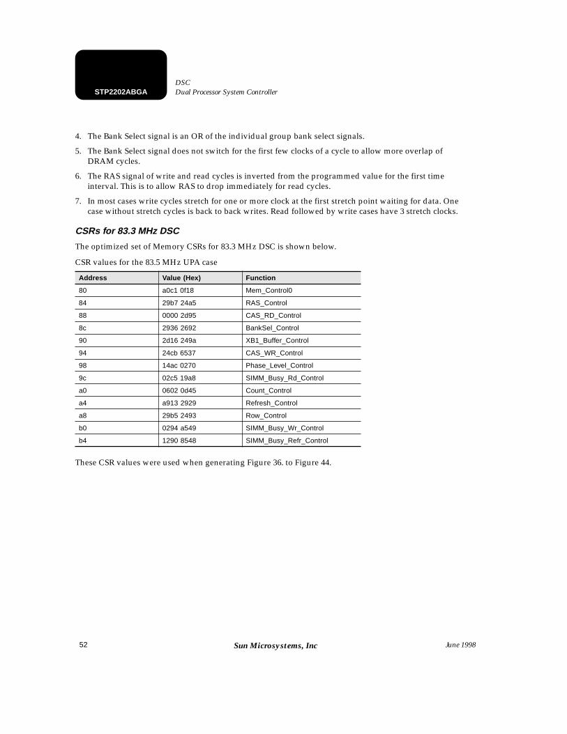
52
STP2202ABGA Dual Processor System Controller DSC
June 1998Sun Microsystems, Inc
4. The Bank Select signal is an OR of the individual group bank select signals.
5. The Bank Select signal does not switch for the first few clocks of a cycle to allow more overlap of DRAM cycles.
6. The RAS signal of write and read cycles is inverted from the programmed value for the first time interval. This is to allow RAS to drop immediately for read cycles.
7. In most cases write cycles stretch for one or more clock at the first stretch point waiting for data. One case without stretch cycles is back to back writes. Read followed by write cases have 3 stretch clocks.
CSRs for 83.3 MHz DSC
The optimized set of Memory CSRs for 83.3 MHz DSC is shown below.
These CSR values were used when generating Figure 36. to Figure 44.
CSR values for the 83.5 MHz UPA case
Address Value (Hex) Function
80 a0c1 0f18 Mem_Control0
84 29b7 24a5 RAS_Control
88 0000 2d95 CAS_RD_Control
8c 2936 2692 BankSel_Control
90 2d16 249a XB1_Buffer_Control
94 24cb 6537 CAS_WR_Control
98 14ac 0270 Phase_Level_Control
9c 02c5 19a8 SIMM_Busy_Rd_Control
a0 0602 0d45 Count_Control
a4 a913 2929 Refresh_Control
a8 29b5 2493 Row_Control
b0 0294 a549 SIMM_Busy_Wr_Control
b4 1290 8548 SIMM_Busy_Refr_Control
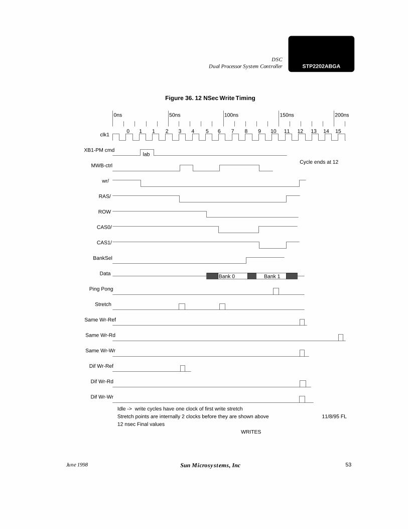
53
Dual Processor System ControllerDSC
STP2202ABGA
June 1998 Sun Microsystems, Inc
Figure 36. 12 NSec Write Timing
0 1 1 2 3 4 5 6 7 8 9 10 11 12 13 14
WRITES
11/8/95 FL
12 nsec Final values
Bank 1Bank 0
15
Cycle ends at 12
lab
Idle -> write cycles have one clock of first write stretch
Stretch points are internally 2 clocks before they are shown above
0ns 50ns 100ns 150ns 200ns
clk1
XB1-PM cmd
MWB-ctrl
wr/
RAS/
ROW
CAS0/
CAS1/
BankSel
Data
Ping Pong
Stretch
Same Wr-Ref
Same Wr-Rd
Same Wr-Wr
Dif Wr-Ref
Dif Wr-Rd
Dif Wr-Wr
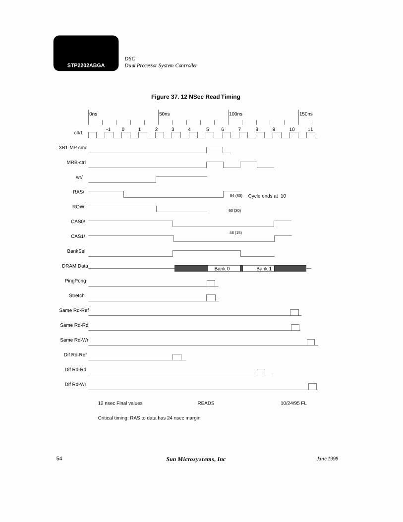
54
STP2202ABGA Dual Processor System Controller DSC
June 1998Sun Microsystems, Inc
Figure 37. 12 NSec Read Timing
-1 0 1 2 3 4 5 6 7 8
12 nsec Final values READS 10/24/95 FL
9 10
Bank 0 Bank 1
11
Cycle ends at 1084 (60)
60 (30)
48 (15)
Critical timing: RAS to data has 24 nsec margin
0ns 50ns 100ns 150ns
clk1
XB1-MP cmd
MRB-ctrl
wr/
RAS/
ROW
CAS0/
CAS1/
BankSel
DRAM Data
PingPong
Stretch
Same Rd-Ref
Same Rd-Rd
Same Rd-Wr
Dif Rd-Ref
Dif Rd-Rd
Dif Rd-Wr
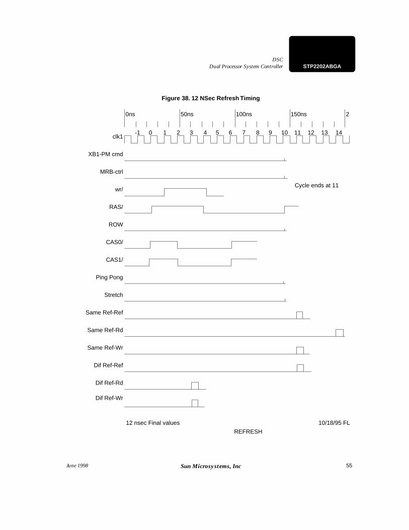
55
Dual Processor System ControllerDSC
STP2202ABGA
June 1998 Sun Microsystems, Inc
Figure 38. 12 NSec Refresh Timing
4 5 6
12 nsec Final values 10/18/95 FL
7 108 9-1 0 1 32 11 12 13 14
REFRESH
Cycle ends at 11
0ns 50ns 100ns 150ns 2
clk1
XB1-PM cmd
MRB-ctrl
wr/
RAS/
ROW
CAS0/
CAS1/
Ping Pong
Stretch
Same Ref-Ref
Same Ref-Rd
Same Ref-Wr
Dif Ref-Ref
Dif Ref-Rd
Dif Ref-Wr
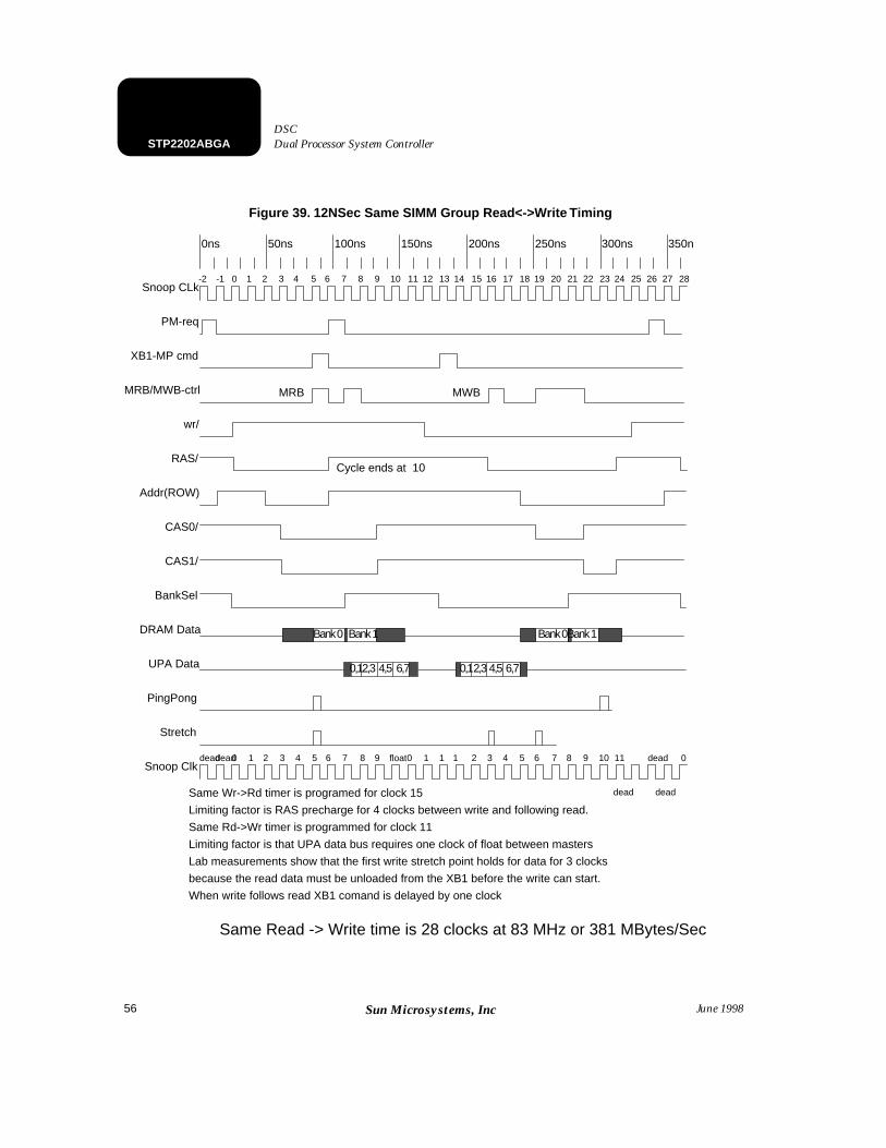
56
STP2202ABGA Dual Processor System Controller DSC
June 1998Sun Microsystems, Inc
Figure 39. 12NSec Same SIMM Group Read<->Write Timing
-1 0 1 2 3 4 5 6 7 8 9 10
Bank 0 Bank 1
11
Cycle ends at 10
0,12,3 4,5 6,7
12-2
5 6 7 9 float0 1 1 2 43 5
Bank 0Bank 1
0,12,3 4,5 6,7
Limiting factor is RAS precharge for 4 clocks between write and following read.
Same Read -> Write time is 28 clocks at 83 MHz or 381 MBytes/Sec
Same Rd->Wr timer is programmed for clock 11
13 14 15 16
deaddead0 1 2 3 4 8 1 6 7
17 18 19 20
Lab measurements show that the first write stretch point holds for data for 3 clocks
Same Wr->Rd timer is programed for clock 15
Limiting factor is that UPA data bus requires one clock of float between masters
21 22 23 24
8 9 10 11
dead
25 26 27 28
dead 0
dead
MWBMRB
because the read data must be unloaded from the XB1 before the write can start.
When write follows read XB1 comand is delayed by one clock
0ns 50ns 100ns 150ns 200ns 250ns 300ns 350n
Snoop CLk
PM-req
XB1-MP cmd
MRB/MWB-ctrl
wr/
RAS/
Addr(ROW)
CAS0/
CAS1/
BankSel
DRAM Data
UPA Data
PingPong
Stretch
Snoop Clk
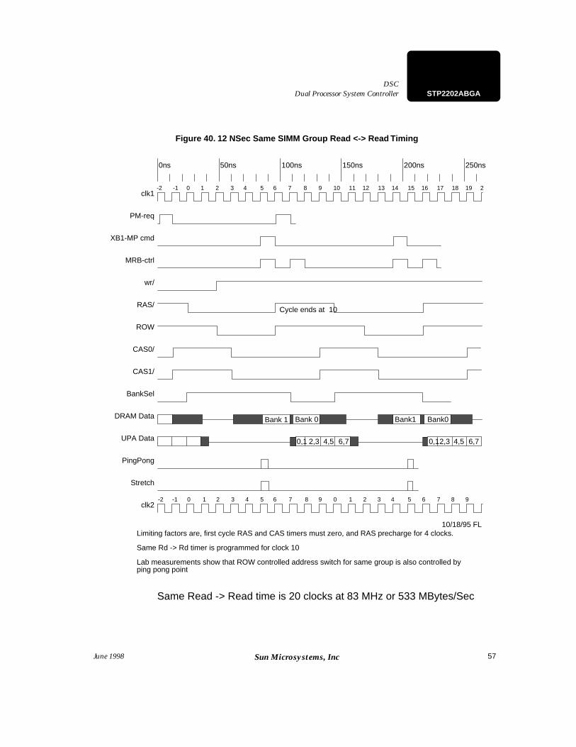
57
Dual Processor System ControllerDSC
STP2202ABGA
June 1998 Sun Microsystems, Inc
Figure 40. 12 NSec Same SIMM Group Read <-> Read Timing
-1 0 1 2 3 4 5 6 7 8 9 10
Bank 1 Bank 0
11
Cycle ends at 10
0,1 2,3 4,5 6,7
12-2
5 6 7 9 0 1 3 4 5 76 8
Bank1 Bank0
0,12,3 4,5 6,7
Limiting factors are, first cycle RAS and CAS timers must zero, and RAS precharge for 4 clocks.
Same Read -> Read time is 20 clocks at 83 MHz or 533 MBytes/Sec
Same Rd -> Rd timer is programmed for clock 10
13 14 15 16
10/18/95 FL
-2 -1 0 1 2 3 4 8 2 9
17 18 19 2
Lab measurements show that ROW controlled address switch for same group is also controlled by
0ns 50ns 100ns 150ns 200ns 250ns
clk1
PM-req
XB1-MP cmd
MRB-ctrl
wr/
RAS/
ROW
CAS0/
CAS1/
BankSel
DRAM Data
UPA Data
PingPong
Stretch
clk2
ping pong point
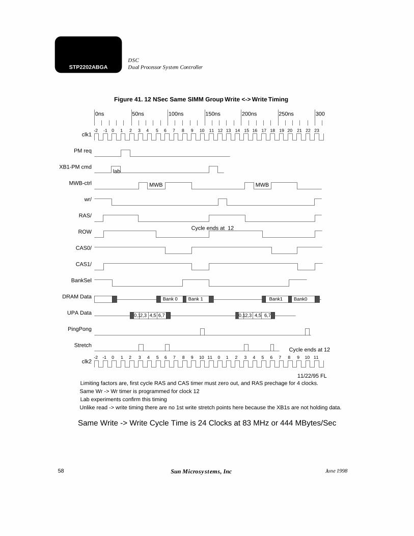
58
STP2202ABGA Dual Processor System Controller DSC
June 1998Sun Microsystems, Inc
Figure 41. 12 NSec Same SIMM Group Write <-> Write Timing
-1 0 1 2 3 4 5 6 7 8 9 10
Bank 0 Bank 1
11
Cycle ends at 12
0,12,3 4,5 6,7
12-2
1 3 54 6
Bank1 Bank0
0,12,3 4,5 6,7
Limiting factors are, first cycle RAS and CAS timer must zero out, and RAS prechage for 4 clocks.
7 8 9 10 11
13
Same Wr -> Wr timer is programmed for clock 12
14 15 16 17 18 19 20 21 22 23
lab
1110 0
Lab experiments confirm this timing
Same Write -> Write Cycle Time is 24 Clocks at 83 MHz or 444 MBytes/Sec
Cycle ends at 12-2 -1
MWB MWB
11/22/95 FL
0 1 2 3 4 5 76 8 9 2
Unlike read -> write timing there are no 1st write stretch points here because the XB1s are not holding data.
0ns 50ns 100ns 150ns 200ns 250ns 300
clk1
PM req
XB1-PM cmd
MWB-ctrl
wr/
RAS/
ROW
CAS0/
CAS1/
BankSel
DRAM Data
UPA Data
PingPong
Stretch
clk2
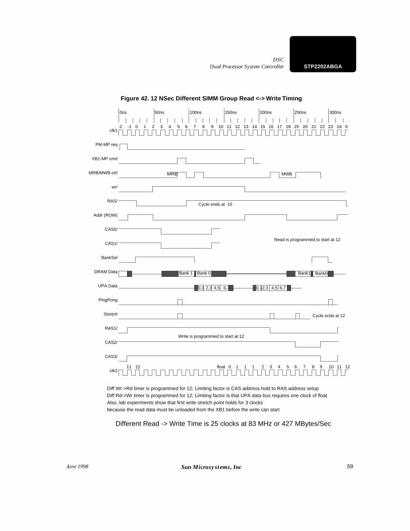
59
Dual Processor System ControllerDSC
STP2202ABGA
June 1998 Sun Microsystems, Inc
Figure 42. 12 NSec Different SIMM Group Read <-> Write Timing
-1 0 1 2 3 4 5 6 7 8 9 10
Bank 1 Bank 0
11
Cycle ends at 10
0,1 2,3 4,5 6,7
12-2
0 1 1 1 2 43 5
Bank1 Bank0
0,12,3 4,5 6,7
Diff Rd->Wr timer is programmed for 12; Limiting factor is that UPA data bus requires one clock of float
Also, lab experiments show that first write stretch point holds for 3 clocks
6 7 8 9 10 11
13
Diff Wr->Rd timer is programmed for 12; Limiting factor is CAS address hold to RAS address setup
14 15 16 17 18 19 20 21 22 23 24
Write is programmed to start at 12
float
Different Read -> Write Time is 25 clocks at 83 MHz or 427 MBytes/Sec
0
121211
MRB MWB
Read is programmed to start at 12
Cycle ends at 12
because the read data must be unloaded from the XB1 before the write can start
0ns 50ns 100ns 150ns 200ns 250ns 300ns
clk1
PM-MP req
XB1-MP cmd
MRB/MWB-ctrl
wr/
RAS/
Addr (ROW)
CAS0/
CAS1/
BankSel
DRAM Data
UPA Data
PingPong
Stretch
RAS1/
CAS2/
CAS3/
clk2
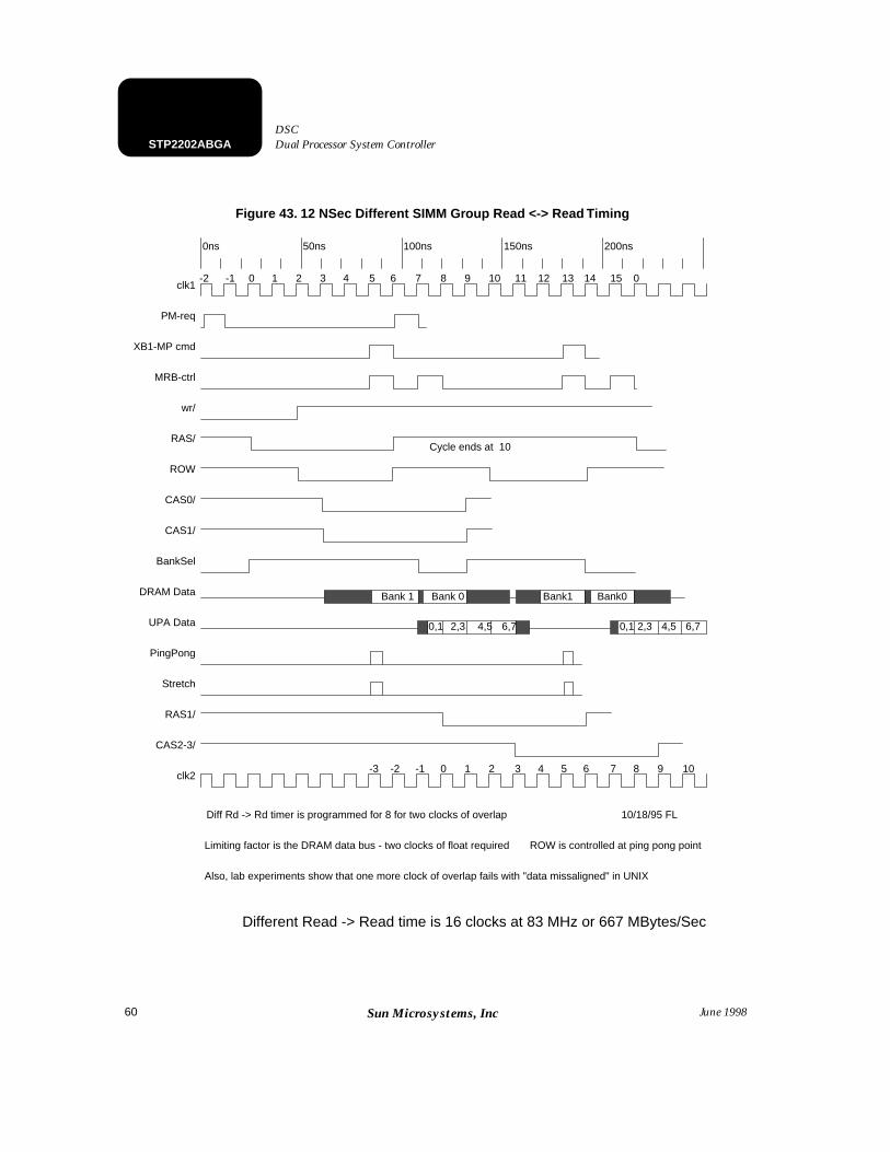
60
STP2202ABGA Dual Processor System Controller DSC
June 1998Sun Microsystems, Inc
Figure 43. 12 NSec Different SIMM Group Read <-> Read Timing
-1 0 1 2 3 4 5 6 7 8 9 10
Bank 1 Bank 0
11
Cycle ends at 10
0,1 2,3 4,5 6,7
12-2
-3 -2 -1 0 1 2 3 4 5 6 7 98 10
Bank1 Bank0
0,1 2,3 4,5 6,7
Limiting factor is the DRAM data bus - two clocks of float required ROW is controlled at ping pong point
Also, lab experiments show that one more clock of overlap fails with "data missaligned" in UNIX
Different Read -> Read time is 16 clocks at 83 MHz or 667 MBytes/Sec
Diff Rd -> Rd timer is programmed for 8 for two clocks of overlap
13 14 15 0
10/18/95 FL
0ns 50ns 100ns 150ns 200ns
clk1
PM-req
XB1-MP cmd
MRB-ctrl
wr/
RAS/
ROW
CAS0/
CAS1/
BankSel
DRAM Data
UPA Data
PingPong
Stretch
RAS1/
CAS2-3/
clk2
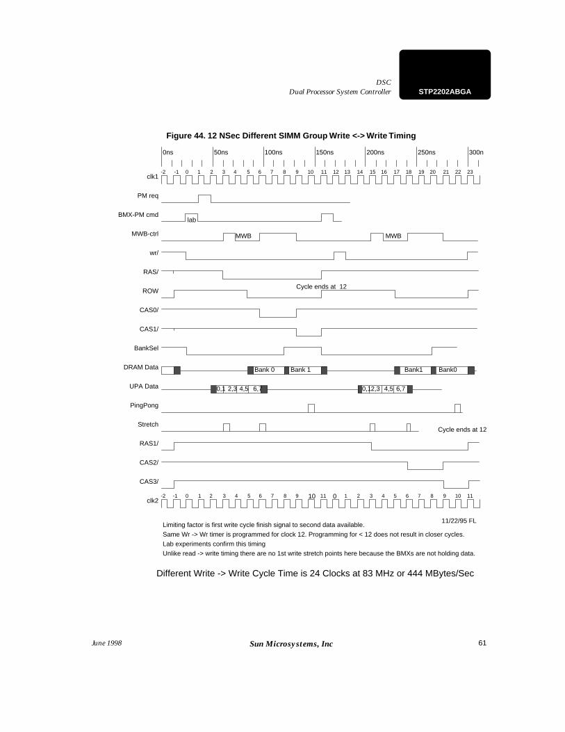
61
Dual Processor System ControllerDSC
STP2202ABGA
June 1998 Sun Microsystems, Inc
Figure 44. 12 NSec Different SIMM Group Write <-> Write Timing
-1 0 1 2 3 4 5 6 7 8 9 10
Bank 0 Bank 1
11
Cycle ends at 12
0,1 2,3 4,5 6,7
12-2
1 3 54 6
Bank1 Bank0
0,12,3 4,5 6,7
Limiting factor is first write cycle finish signal to second data available.
7 8 9 10 11
13
Same Wr -> Wr timer is programmed for clock 12. Programming for < 12 does not result in closer cycles.
14 15 16 17 18 19 20 21 22 23
lab
1110 0
Lab experiments confirm this timing
Different Write -> Write Cycle Time is 24 Clocks at 83 MHz or 444 MBytes/Sec
Cycle ends at 12
-2 -1
MWB MWB
11/22/95 FL
0 1 2 3 4 5 76 8 9 2
Unlike read -> write timing there are no 1st write stretch points here because the BMXs are not holding data.
0ns 50ns 100ns 150ns 200ns 250ns 300n
clk1
PM req
BMX-PM cmd
MWB-ctrl
wr/
RAS/
ROW
CAS0/
CAS1/
BankSel
DRAM Data
UPA Data
PingPong
Stretch
RAS1/
CAS2/
CAS3/
clk2
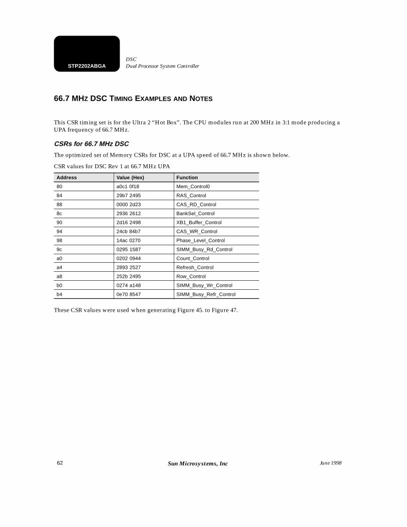
62
STP2202ABGA Dual Processor System Controller DSC
June 1998Sun Microsystems, Inc
66.7 MHZ DSC TIMING EXAMPLES AND NOTES
This CSR timing set is for the Ultra 2 “Hot Box”. The CPU modules run at 200 MHz in 3:1 mode producing a UPA frequency of 66.7 MHz.
CSRs for 66.7 MHz DSC
The optimized set of Memory CSRs for DSC at a UPA speed of 66.7 MHz is shown below.
These CSR values were used when generating Figure 45. to Figure 47.
CSR values for DSC Rev 1 at 66.7 MHz UPA
Address Value (Hex) Function
80 a0c1 0f18 Mem_Control0
84 29b7 2495 RAS_Control
88 0000 2d23 CAS_RD_Control
8c 2936 2612 BankSel_Control
90 2d16 2498 XB1_Buffer_Control
94 24cb 84b7 CAS_WR_Control
98 14ac 0270 Phase_Level_Control
9c 0295 1587 SIMM_Busy_Rd_Control
a0 0202 0944 Count_Control
a4 2893 2527 Refresh_Control
a8 252b 2495 Row_Control
b0 0274 a148 SIMM_Busy_Wr_Control
b4 0e70 8547 SIMM_Busy_Refr_Control
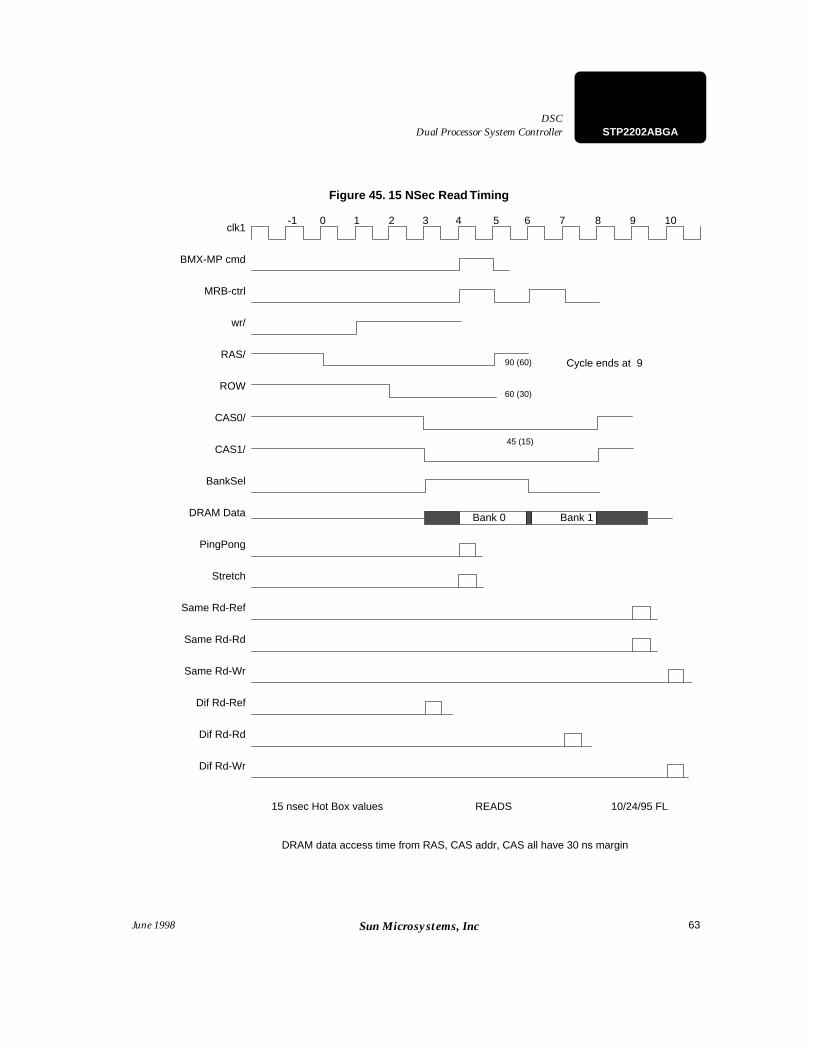
63
Dual Processor System ControllerDSC
STP2202ABGA
June 1998 Sun Microsystems, Inc
Figure 45. 15 NSec Read Timing
-1 0 1 2 3 4 5 6 7 8
15 nsec Hot Box values READS 10/24/95 FL
9 10
Bank 0 Bank 1
Cycle ends at 9
DRAM data access time from RAS, CAS addr, CAS all have 30 ns margin
90 (60)
60 (30)
45 (15)
clk1
BMX-MP cmd
MRB-ctrl
wr/
RAS/
ROW
CAS0/
CAS1/
BankSel
DRAM Data
PingPong
Stretch
Same Rd-Ref
Same Rd-Rd
Same Rd-Wr
Dif Rd-Ref
Dif Rd-Rd
Dif Rd-Wr
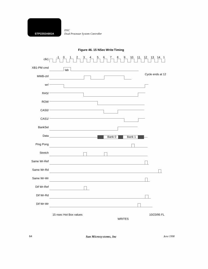
64
STP2202ABGA Dual Processor System Controller DSC
June 1998Sun Microsystems, Inc
Figure 46. 15 NSec Write Timing
-1 0 1 2 3 4 5 6 7 8 9 10 11 12 13 14
WRITES
10/23/95 FL15 nsec Hot Box values
Bank 1Bank 0
1
Cycle ends at 12
lab
clk1
XB1-PM cmd
MWB-ctrl
wr/
RAS/
ROW
CAS0/
CAS1/
BankSel
Data
Ping Pong
Stretch
Same Wr-Ref
Same Wr-Rd
Same Wr-Wr
Dif Wr-Ref
Dif Wr-Rd
Dif Wr-Wr
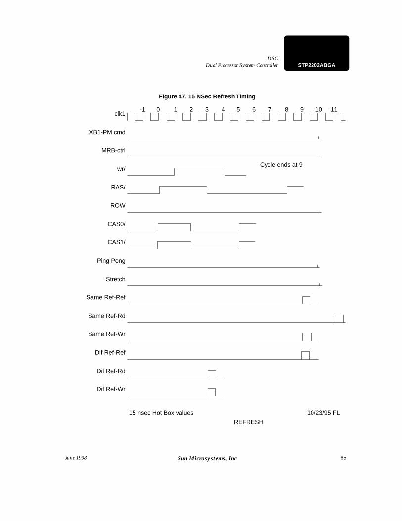
65
Dual Processor System ControllerDSC
STP2202ABGA
June 1998 Sun Microsystems, Inc
Figure 47. 15 NSec Refresh Timing
4 5 6
15 nsec Hot Box values 10/23/95 FL
7 108 9-1 0 1 32 11
REFRESH
Cycle ends at 9
clk1
XB1-PM cmd
MRB-ctrl
wr/
RAS/
ROW
CAS0/
CAS1/
Ping Pong
Stretch
Same Ref-Ref
Same Ref-Rd
Same Ref-Wr
Dif Ref-Ref
Dif Ref-Rd
Dif Ref-Wr
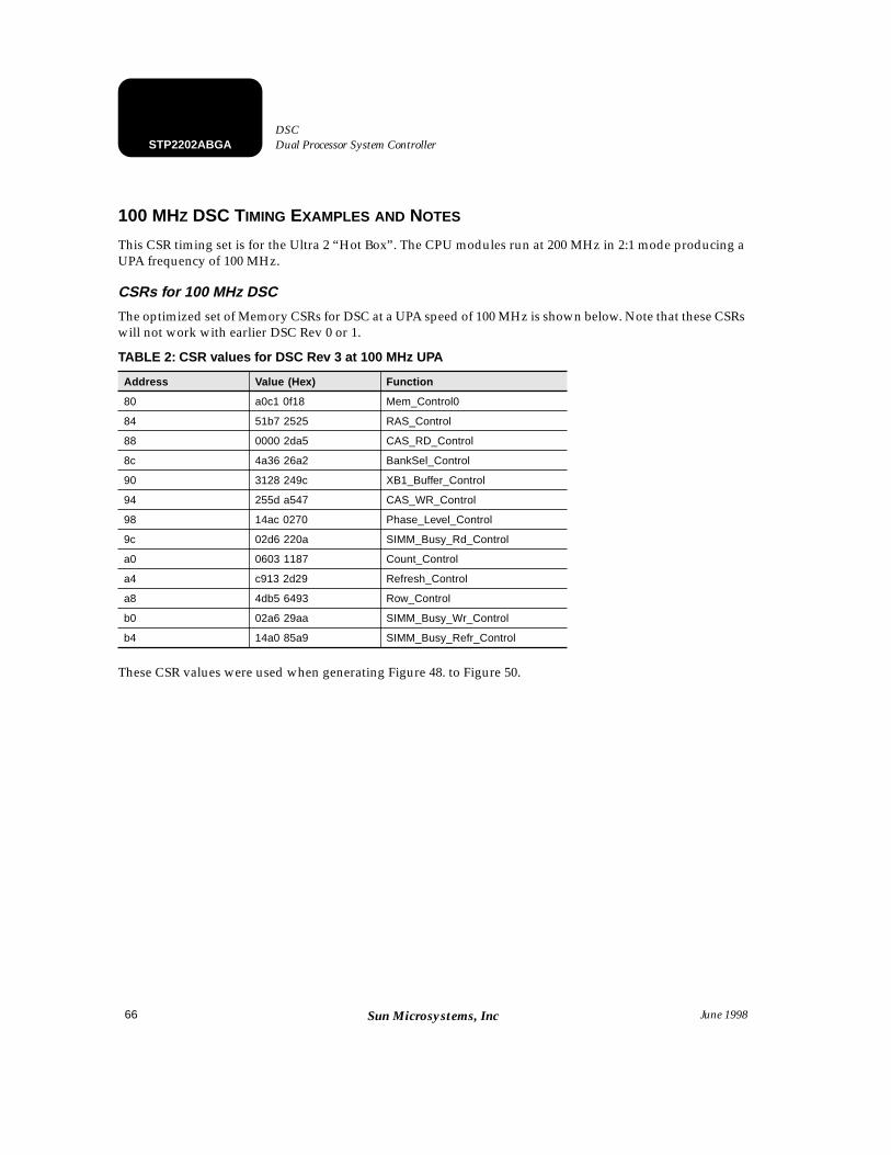
66
STP2202ABGA Dual Processor System Controller DSC
June 1998Sun Microsystems, Inc
100 MHZ DSC TIMING EXAMPLES AND NOTES
This CSR timing set is for the Ultra 2 “Hot Box”. The CPU modules run at 200 MHz in 2:1 mode producing a UPA frequency of 100 MHz.
CSRs for 100 MHz DSC
The optimized set of Memory CSRs for DSC at a UPA speed of 100 MHz is shown below. Note that these CSRs will not work with earlier DSC Rev 0 or 1.
These CSR values were used when generating Figure 48. to Figure 50.
TABLE 2: CSR values for DSC Rev 3 at 100 MHz UPA
Address Value (Hex) Function
80 a0c1 0f18 Mem_Control0
84 51b7 2525 RAS_Control
88 0000 2da5 CAS_RD_Control
8c 4a36 26a2 BankSel_Control
90 3128 249c XB1_Buffer_Control
94 255d a547 CAS_WR_Control
98 14ac 0270 Phase_Level_Control
9c 02d6 220a SIMM_Busy_Rd_Control
a0 0603 1187 Count_Control
a4 c913 2d29 Refresh_Control
a8 4db5 6493 Row_Control
b0 02a6 29aa SIMM_Busy_Wr_Control
b4 14a0 85a9 SIMM_Busy_Refr_Control
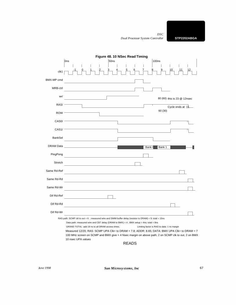
67
Dual Processor System ControllerDSC
STP2202ABGA
June 1998 Sun Microsystems, Inc
Figure 48. 10 NSec Read Timing
-1 0 1 2 3 4 5 6 7 8
10 nsec UPA values
READS
9 10
Bank 0 Bank 1
11
Cycle ends at 11
12
RAS path: SCMP ckl to out = 6 ; measured wire and SIMM buffer delay (resistor to DRAM) = 9; total = 15ns
Data path: measured wire and CBT delay (DRAM to BMX) = 4 ; BMX setup = 4ns; total = 8ns
GRAND TOTAL: add 19 ns to all DRAM access times.
80 (60)
60 (30)
Limiting factor is RAS to data: 1 ns margin
Measured 12/20; RAS: SCMP UPA Clk+ to DRAM = 7.8; ADDR: 8.65; DATA: BMX UPA Clk+ to DRAM = 7.
100 MHz screen on SCMP and BMX give + 4 Nsec margin on above path; 2 on SCMP clk to out, 2 on BMX
this is 23 @ 12nsec
0ns 50ns 100ns
clk1
BMX-MP cmd
MRB-ctrl
wr/
RAS/
ROW
CAS0/
CAS1/
BankSel
DRAM Data
PingPong
Stretch
Same Rd-Ref
Same Rd-Rd
Same Rd-Wr
Dif Rd-Ref
Dif Rd-Rd
Dif Rd-Wr
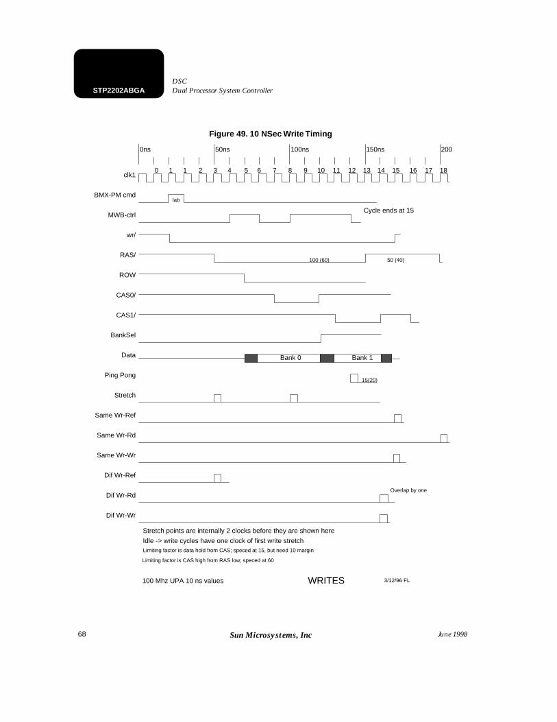
68
STP2202ABGA Dual Processor System Controller DSC
June 1998Sun Microsystems, Inc
Figure 49. 10 NSec Write Timing
0 1 1 2 3 4 5 6 7 8 9 10 11 12 13 14
WRITES 3/12/96 FL100 Mhz UPA 10 ns values
Bank 1Bank 0
15
Cycle ends at 15
lab
16 17 18
Limiting factor is data hold from CAS; speced at 15, but need 10 margin
Limiting factor is CAS high from RAS low; speced at 60
100 (60)
Stretch points are internally 2 clocks before they are shown here
Idle -> write cycles have one clock of first write stretch
Overlap by one
50 (40)
15(20)
0ns 50ns 100ns 150ns 200
clk1
BMX-PM cmd
MWB-ctrl
wr/
RAS/
ROW
CAS0/
CAS1/
BankSel
Data
Ping Pong
Stretch
Same Wr-Ref
Same Wr-Rd
Same Wr-Wr
Dif Wr-Ref
Dif Wr-Rd
Dif Wr-Wr

69
Dual Processor System ControllerDSC
STP2202ABGA
June 1998 Sun Microsystems, Inc
Figure 50. 10 NSec Refresh Timing
4 5 6
100 MHz UPA values 1/3/96 FL
7 108 9-1 0 1 32 11 12 13 14 15
REFRESH
Cycle ends at 12
0ns 50ns 100ns 150ns
clk1
BMX-PM cmd
MRB-ctrl
wr/
RAS/
ROW
CAS0/
CAS1/
Ping Pong
Stretch
Same Ref-Ref
Same Ref-Rd
Same Ref-Wr
Dif Ref-Ref
Dif Ref-Rd
Dif Ref-Wr
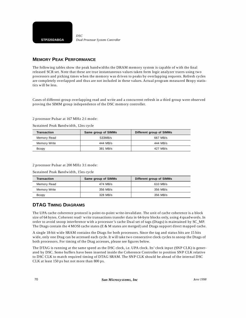
70
STP2202ABGA Dual Processor System Controller DSC
June 1998Sun Microsystems, Inc
MEMORY PEAK PERFORMANCE
The following tables show the peak bandwidths the DRAM memory system is capable of with the final released SCR set. Note that these are true instantaneous values taken form logic analyzer traces using two processors and picking times when the memory was driven to peaks by overlapping requests. Refresh cycles are completely overlapped and thus are not included in these values. Actual program measured Bcopy statis-tics will be less.
Cases of different group overlapping read and write and a concurrent refresh in a third group were observed proving the SIMM group independence of the DSC memory controller.
2 processor Pulsar at 167 MHz 2:1 mode:
2 processor Pulsar at 200 MHz 3:1 mode:
DTAG TIMING DIAGRAMS
The UPA cache coherence protocol is point-to-point write-invalidate. The unit of cache coherence is a block size of 64 bytes. Coherent read/write transactions transfer data in 64-byte blocks only, using 4 quadwords. In order to avoid snoop interference with a processor’s cache Dual set of tags (Dtags) is maintained by SC_MP. The Dtags contain the 4 MOSI cache states (E & M states are merged) and Dtags support direct mapped cache.
A single 18-bit wide SRAM contains the Dtags for both processors. Since the tag and status bits are 15 bits wide, only one Dtag can be accessed each cycle. It will take two consecutive clock cycles to snoop the Dtags of both processors. For timing of the Dtag accesses, please see figures below.
The DTAG is running at the same speed as the DSC clock, i.e. UPA clock. Its’ clock input (SNP CLK) is gener-ated by DSC. Some buffers have been inserted inside the Coherence Controller to position SNP CLK relative to DSC CLK to match required timing of DTAG SRAM. The SNP CLK should be ahead of the internal DSC CLK at least 150 ps but not more than 800 ps.
Sustained Peak Bandwidth, 12ns cycle
Transaction Same group of SIMMs Different group of SIMMs
Memory Read 533MB/s 667 MB/s
Memory Write 444 MB/s 444 MB/s
Bcopy 381 MB/s 427 MB/s
Sustained Peak Bandwidth, 15ns cycle
Transaction Same group of SIMMs Different group of SIMMs
Memory Read 474 MB/s 610 MB/s
Memory Write 356 MB/s 356 MB/s
Bcopy 328 MB/s 356 MB/s
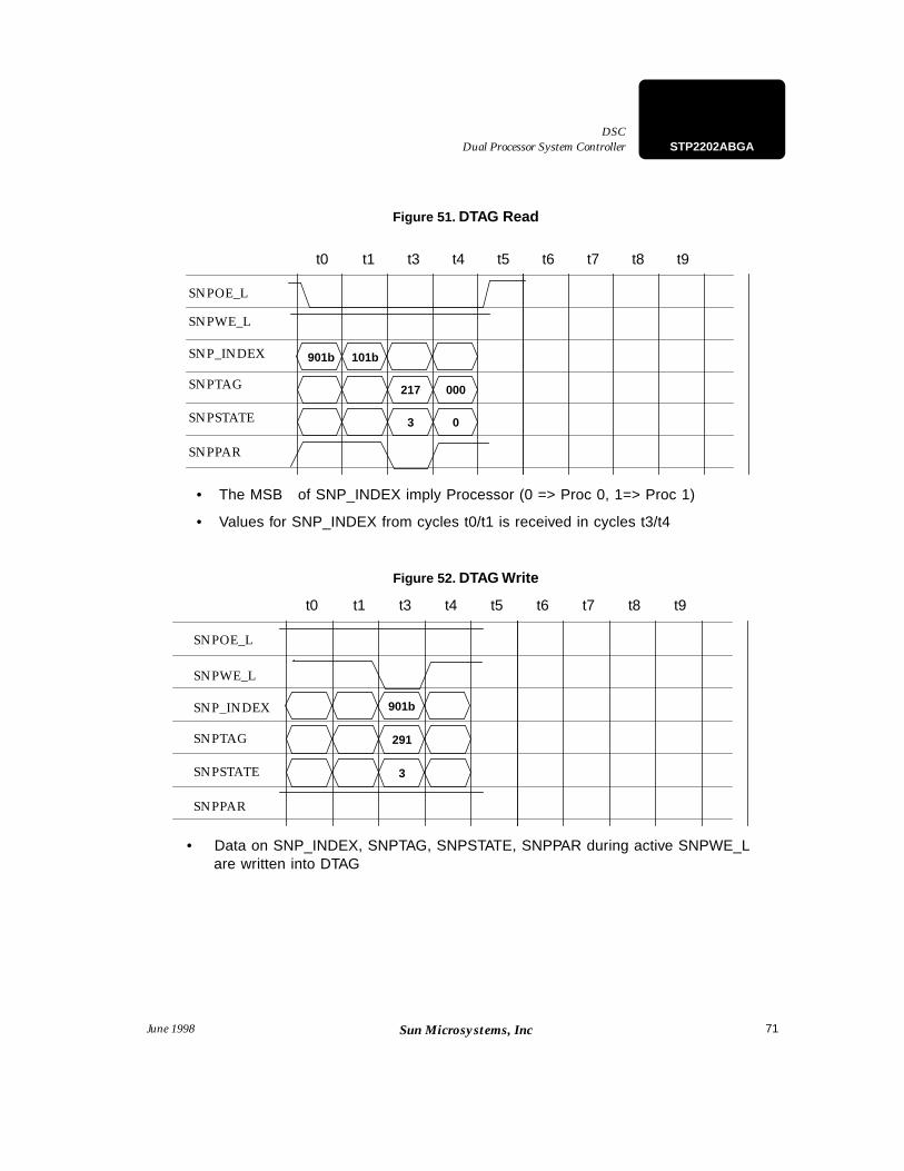
71
Dual Processor System ControllerDSC
STP2202ABGA
June 1998 Sun Microsystems, Inc
Figure 51. DTAG Read
Figure 52. DTAG Write
• The MSB of SNP_INDEX imply Processor (0 => Proc 0, 1=> Proc 1)
• Values for SNP_INDEX from cycles t0/t1 is received in cycles t3/t4
t0
901b 101b
217 000
t1 t3 t4 t5 t6 t7 t8 t9
3 0
SNPOE_L
SNPWE_L
SNP_INDEX
SNPTAG
SNPSTATE
SNPPAR
t0
901b
291
t1 t3 t4 t5 t6 t7 t8 t9
3
• Data on SNP_INDEX, SNPTAG, SNPSTATE, SNPPAR during active SNPWE_L are written into DTAG
SNPOE_L
SNPWE_L
SNP_INDEX
SNPTAG
SNPSTATE
SNPPAR
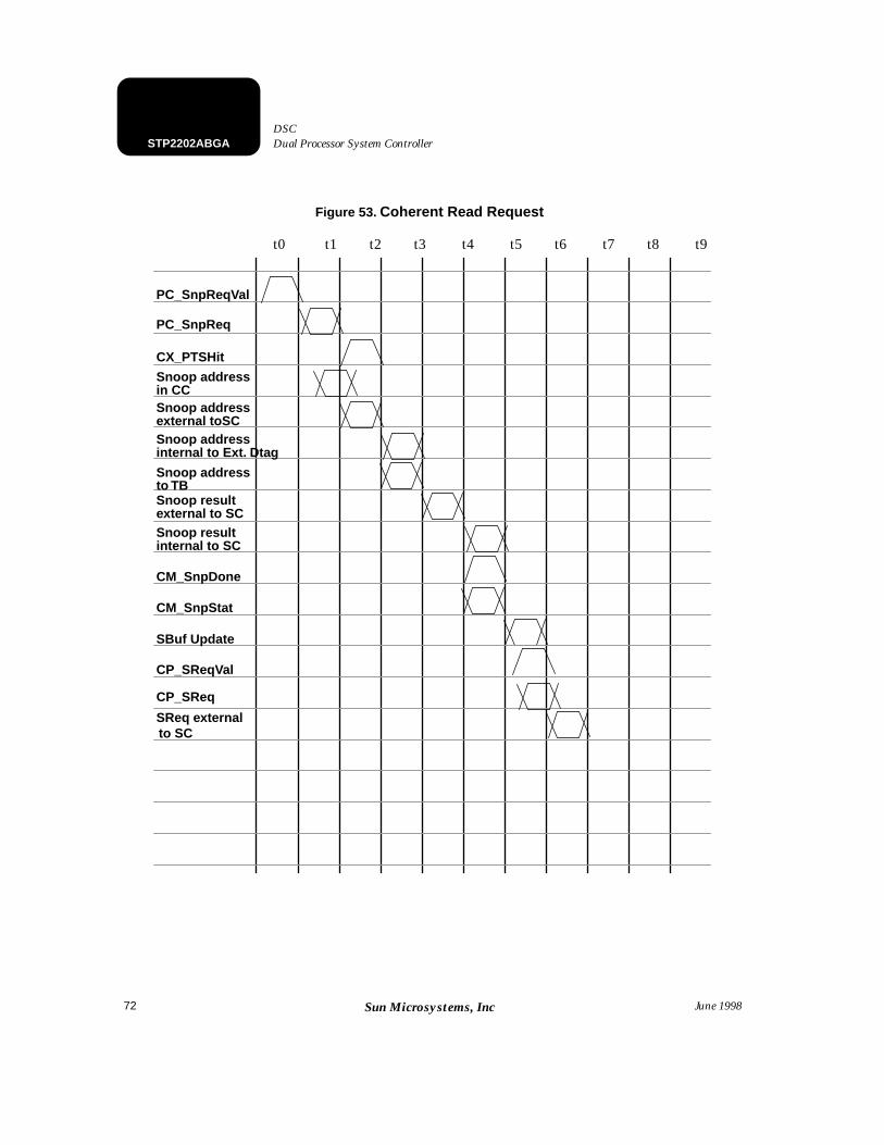
72
STP2202ABGA Dual Processor System Controller DSC
June 1998Sun Microsystems, Inc
Figure 53. Coherent Read Request
PC_SnpReqVal
PC_SnpReq
Snoop address
Snoop result
Snoop address
CX_PTSHit
Snoop address
t0 t1 t2 t3 t4 t5 t6 t7 t8 t9
Snoop address
Snoop result
CM_SnpDone
CM_SnpStat
SBuf Update
CP_SReqVal
CP_SReq
SReq external
in CC
external toSC
internal to Ext. Dtag
external to SC
internal to SC
to SC
to TB
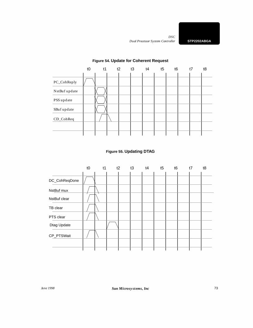
73
Dual Processor System ControllerDSC
STP2202ABGA
June 1998 Sun Microsystems, Inc
Figure 54. Update for Coherent Request
Figure 55. Updating DTAG
t0 t1 t2 t3 t4 t5 t6 t7 t8
PC_CohReply
NstBuf update
PSS update
SBuf update
CD_CohReq
t0 t1 t2 t3 t4 t5 t6 t7 t8
DC_CohReqDone
NstBuf mux
NstBuf clear
TB clear
PTS clear
Dtag Update
CP_PTSWait
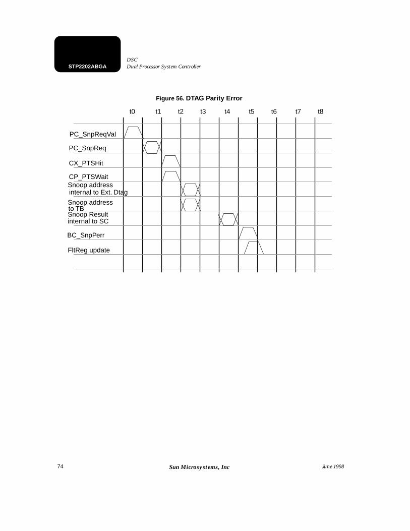
74
STP2202ABGA Dual Processor System Controller DSC
June 1998Sun Microsystems, Inc
Figure 56. DTAG Parity Error
Snoop address
Snoop Result
t0 t1 t2 t3 t4 t5 t6 t7 t8
internal to Ext. Dtag
internal to SC
BC_SnpPerr
FltReg update
Snoop address
CP_PTSWait
CX_PTSHit
PC_SnpReq
PC_SnpReqVal
to TB
75
Dual Processor System ControllerDSC
STP2202ABGA
June 1998 Sun Microsystems, Inc
Figure 57. Four Consecutive RDS from P0 with DTAGs in I, S, O and M States
Sys
tem
s S
cien
ce In
c. -
Sim
Wav
e 2.
5A.3
Tue
Oct
31
14:2
0:30
199
5
time
(ns)
sc_s
ubsy
s.U
PA
_AV
0
sc_s
ubsy
s.U
PA
_A0
sc_s
ubsy
s.U
PA
_SC
RE
Q00
sc_s
ubsy
s.S
RE
PLY
sc_s
ubsy
s.P
RE
PLY
sc_s
ubsy
s.sc
.Xsc
mp_
top.
PC
_Snp
Req
Val
sc_s
ubsy
s.sc
.Xsc
mp_
top.
CX
_Ret
ry
sc_s
ubsy
s.sc
.Xsc
mp_
top.
PM
_Req
Val
sc_s
ubsy
s.sc
.Xsc
mp_
top.
PM
_Rea
d
sc_s
ubsy
s.sc
.Xsc
mp_
top.
ME
_RA
S_L
sc_s
ubsy
s.sc
.Xsc
mp_
top.
ME
_CA
S_L
sc_s
ubsy
s.B
AN
K_S
EL
sc_s
ubsy
s.B
MX
CM
D0
sc_s
ubsy
s.B
MX
CM
D1
sc_s
ubsy
s.M
RB
CTR
L1
sc_s
ubsy
s.S
NP
OE
_L
sc_s
ubsy
s.S
NP
WE
_L
sc_s
ubsy
s.S
NP
_IN
DE
X
sc_s
ubsy
s.S
NP
TAG
sc_s
ubsy
s.S
NP
STA
TE
sc_s
ubsy
s.S
NP
PA
R
01
01
01
02
01
02
0
0200
0000
c00
0000
000
0000
0000
400
0000
008
0000
0000
800
0000
00c
0000
0000
c
0000
000
000
0000
000
000
0000
0
0000
000
000
0000
0
fe
fe
fe
fe
fb
f
fcff
fcff
fcff
fcff
fcff
cfff
0f
0f
0f
0f
0f
0
040
40
40
040
40
40
0000
0000
0000
0000
0000
0000
0000
0000
0000
0000
001
000
03
03
10
13
20
12
30
12
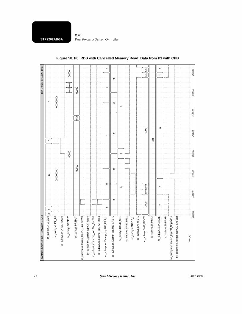
76
STP2202ABGA Dual Processor System Controller DSC
June 1998Sun Microsystems, Inc
Figure 58. P0: RDS with Cancelled Memory Read; Data from P1 with CPB
Sys
tem
s S
cien
ce In
c. -
Sim
Wav
e 2.
5A.3
Tue
Oct
31
15:3
4:29
199
5
time
(ns)
2392
0.00
2396
8.00
2401
6.00
2406
4.00
2411
2.00
2416
0.00
2420
8.00
2425
6.00
sc_s
ubsy
s.U
PA
_AV
0
sc_s
ubsy
s.U
PA
_A0
sc_s
ubsy
s.U
PA
_SC
RE
Q00
sc_s
ubsy
s.S
RE
PLY
sc_s
ubsy
s.P
RE
PLY
sc_s
ubsy
s.sc
.Xsc
mp_
top.
PC
_Snp
Req
Val
sc_s
ubsy
s.sc
.Xsc
mp_
top.
CX
_Ret
ry
sc_s
ubsy
s.sc
.Xsc
mp_
top.
PM
_Req
Val
sc_s
ubsy
s.sc
.Xsc
mp_
top.
PM
_Rea
d
sc_s
ubsy
s.sc
.Xsc
mp_
top.
ME
_RA
S_L
sc_s
ubsy
s.sc
.Xsc
mp_
top.
ME
_CA
S_L
sc_s
ubsy
s.B
AN
K_S
EL
sc_s
ubsy
s.M
RB
CTR
L1
sc_s
ubsy
s.S
NP
OE
_L
sc_s
ubsy
s.S
NP
WE
_L
sc_s
ubsy
s.S
NP
_IN
DE
X
sc_s
ubsy
s.S
NP
TAG
sc_s
ubsy
s.S
NP
STA
TE
sc_s
ubsy
s.S
NP
PA
R
sc_s
ubsy
s.sc
.Xsc
mp_
top.
CX
_Snp
RdD
n
sc_s
ubsy
s.sc
.Xsc
mp_
top.
CX
_Snp
Sta
t
01
02
0
0000
0000
c00
0000
00c
0000
000
0400
0009
0000
0
0000
000
140
0000
0
fe
fb
f
fffc
ffcf
ff
0f
0
0000
8003
0003
0000
0003
8003
000
23
01
2
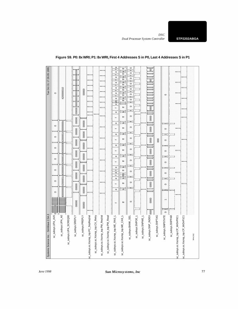
77
Dual Processor System ControllerDSC
STP2202ABGA
June 1998 Sun Microsystems, Inc
Figure 59. P0: 8x WRI; P1: 8x WRI, First 4 Addresses S in P0, Last 4 Addresses S in P1
Sys
tem
s S
cien
ce In
c. -
Sim
Wav
e 2.
5A.3
Tue
Oct
31
17:2
6:05
199
5
time
(ns)
sc_s
ubsy
s.U
PA
_AV
0
sc_s
ubsy
s.U
PA
_A0
sc_s
ubsy
s.U
PA
_SC
RE
Q00
sc_s
ubsy
s.S
RE
PLY
sc_s
ubsy
s.P
RE
PLY
sc_s
ubsy
s.sc
.Xsc
mp_
top.
PC
_Snp
Req
Val
sc_s
ubsy
s.sc
.Xsc
mp_
top.
CX
_Ret
ry
sc_s
ubsy
s.sc
.Xsc
mp_
top.
PM
_Req
Val
sc_s
ubsy
s.sc
.Xsc
mp_
top.
PM
_Rea
d
sc_s
ubsy
s.sc
.Xsc
mp_
top.
ME
_RA
S_L
sc_s
ubsy
s.sc
.Xsc
mp_
top.
ME
_CA
S_L
sc_s
ubsy
s.B
AN
K_S
EL
sc_s
ubsy
s.S
NP
OE
_L
sc_s
ubsy
s.S
NP
WE
_L
sc_s
ubsy
s.S
NP
_IN
DE
X
sc_s
ubsy
s.S
NP
TAG
sc_s
ubsy
s.S
NP
STA
TE
sc_s
ubsy
s.S
NP
PA
R
sc_s
ubsy
s.sc
.Xsc
mp_
top.
CP
_WrD
nP0C
1
sc_s
ubsy
s.sc
.Xsc
mp_
top.
CP
_WrD
nP1C
1
00
00
00
00
00
4000
0000
042
0000
01c
4000
0000
442
0000
018
4000
0000
842
0000
014
4000
0000
c42
0000
010
0000
000
000
0000
000
000
0000
000
000
0000
000
000
0000
000
000
0000
000
000
0000
000
000
0000
000
000
0000
000
000
0000
000
000
0000
000
000
0000
000
000
0000
0
fe
fe
fd
fe
fe
fe
fe
fe
fe
fe
abe
fe
fe
fe
fe
fe
fe
fffe
fffe
fff3
fffe
fffe
fffe
fffe
fffe
fffe
ffff
feff
feff
feff
feff
feff
feff
0f
0f
0f
0f
0f
0f
0f
0f
0f
0f
0f
0f
0f
0f
0f
0
0000
0000
0000
0000
0000
0000
0000
0000
0000
0000
0000
0000
000
01
11
01
01
01
01
01
01
0
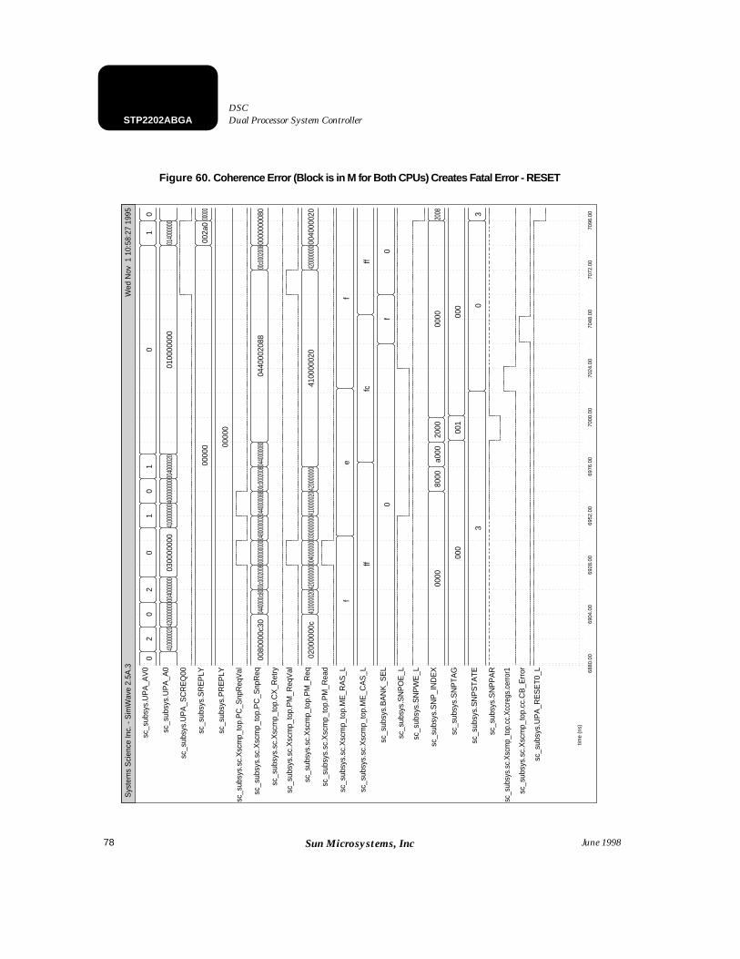
78
STP2202ABGA Dual Processor System Controller DSC
June 1998Sun Microsystems, Inc
Figure 60. Coherence Error (Block is in M for Both CPUs) Creates Fatal Error - RESET
Sys
tem
s S
cien
ce In
c. -
Sim
Wav
e 2.
5A.3
Wed
Nov
1 1
0:58
:27
1995
time
(ns)
6880
.00
6904
.00
6928
.00
6952
.00
6976
.00
7000
.00
7024
.00
7048
.00
7072
.00
7096
.00
sc_s
ubsy
s.U
PA
_AV
0
sc_s
ubsy
s.U
PA
_A0
sc_s
ubsy
s.U
PA
_SC
RE
Q00
sc_s
ubsy
s.S
RE
PLY
sc_s
ubsy
s.P
RE
PLY
sc_s
ubsy
s.sc
.Xsc
mp_
top.
PC
_Snp
Req
Val
sc_s
ubsy
s.sc
.Xsc
mp_
top.
PC
_Snp
Req
sc_s
ubsy
s.sc
.Xsc
mp_
top.
CX
_Ret
ry
sc_s
ubsy
s.sc
.Xsc
mp_
top.
PM
_Req
Val
sc_s
ubsy
s.sc
.Xsc
mp_
top.
PM
_Req
sc_s
ubsy
s.sc
.Xsc
mp_
top.
PM
_Rea
d
sc_s
ubsy
s.sc
.Xsc
mp_
top.
ME
_RA
S_L
sc_s
ubsy
s.sc
.Xsc
mp_
top.
ME
_CA
S_L
sc_s
ubsy
s.B
AN
K_S
EL
sc_s
ubsy
s.S
NP
OE
_L
sc_s
ubsy
s.S
NP
WE
_L
sc_s
ubsy
s.S
NP
_IN
DE
X
sc_s
ubsy
s.S
NP
TAG
sc_s
ubsy
s.S
NP
STA
TE
sc_s
ubsy
s.S
NP
PA
R
sc_s
ubsy
s.sc
.Xsc
mp_
top.
cc.X
ccre
gs.c
erro
r1
sc_s
ubsy
s.sc
.Xsc
mp_
top.
cc.C
B_E
rror
sc_s
ubsy
s.U
PA
_RE
SE
T0_L
02
02
01
01
01
0
4100
0002
0420
0000
0000
4000
000
0300
0000
041
0000
0004
0000
0000
0040
0002
001
0000
000
0140
0000
0
0000
000
2a0
0000
0
0000
0
0080
000c
3004
4000
0c80
00c0
0020
0800
0000
0000
0480
0000
0204
4000
0088
00c0
0020
0804
4000
0080
0440
0020
8800
c000
2008
0000
0000
80
0200
0000
c41
0000
0204
2000
0000
0040
0000
0030
0000
0041
0000
0204
2000
0000
4100
0002
042
0000
0000
0400
0020
fe
f
fffc
ff
0f
0
0000
8000
a000
2000
0000
2008
000
001
000
30
3
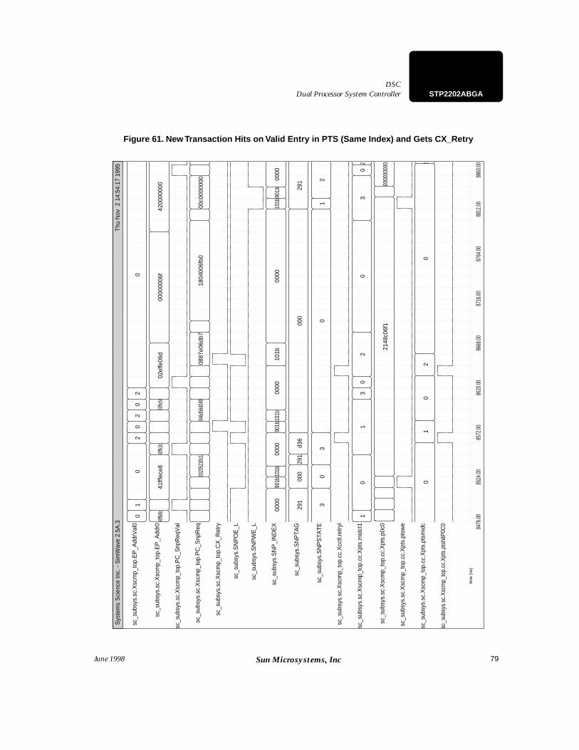
79
Dual Processor System ControllerDSC
STP2202ABGA
June 1998 Sun Microsystems, Inc
Figure 61. New Transaction Hits on Valid Entry in PTS (Same Index) and Gets CX_Retry
Sys
tem
s S
cien
ce In
c. -
Sim
Wav
e 2.
5A.3
Thu
Nov
2 1
4:54
:17
1995
time
(ns)
8476
.0085
24.00
8572
.0086
20.00
8668
.0087
16.00
8764
.0088
12.00
8860
.00
sc_s
ubsy
s.sc
.Xsc
mp_
top.
EP
_Add
rVal
0
sc_s
ubsy
s.sc
.Xsc
mp_
top.
EP
_Add
r0
sc_s
ubsy
s.sc
.Xsc
mp_
top.
PC
_Snp
Req
Val
sc_s
ubsy
s.sc
.Xsc
mp_
top.
PC
_Snp
Req
sc_s
ubsy
s.sc
.Xsc
mp_
top.
CX
_Ret
ry
sc_s
ubsy
s.S
NP
OE
_L
sc_s
ubsy
s.S
NP
WE
_L
sc_s
ubsy
s.S
NP
_IN
DE
X
sc_s
ubsy
s.S
NP
TAG
sc_s
ubsy
s.S
NP
STA
TE
sc_s
ubsy
s.sc
.Xsc
mp_
top.
cc.X
cctl.
retry
i
sc_s
ubsy
s.sc
.Xsc
mp_
top.
cc.X
pts.
mid
ct1
sc_s
ubsy
s.sc
.Xsc
mp_
top.
cc.X
pts.
p0c0
sc_s
ubsy
s.sc
.Xsc
mp_
top.
cc.X
pts.
ptsw
e
sc_s
ubsy
s.sc
.Xsc
mp_
top.
cc.X
pts.
ptsm
idc
sc_s
ubsy
s.sc
.Xsc
mp_
top.
cc.X
pts.
ptsh
itP0C
0
01
02
02
02
0
40fffe0
6c41
fffec
e843f
ffe10c
43fffec
5402
effe
06d
0000
0006
f42
0000
000
0020
5230
c104
6d56
d049
0887
e06d
b718
0400
6fb0
00c0
0000
00
0000
901b
101b
0000
901b
101b
0000
101b
0000
101b
901b
0000
291
000
291
d36
000
291
30
30
12
10
13
02
03
02
2148
c06f
100
0000
000
01
02
02
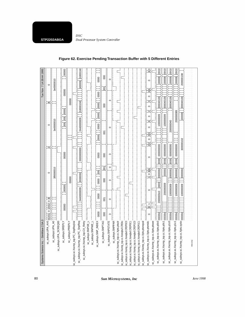
80
STP2202ABGA Dual Processor System Controller DSC
June 1998Sun Microsystems, Inc
Figure 62. Exercise Pending Transaction Buffer with 5 Different Entries
Sys
tem
s S
cien
ce In
c. -
Sim
Wav
e 2.
5A.3
Tue
Nov
7 1
4:39
:44
1995
time
(ns)
sc_s
ubsy
s.U
PA
_AV
0
sc_s
ubsy
s.U
PA
_A0
sc_s
ubsy
s.U
PA
_SC
RE
Q00
sc_s
ubsy
s.S
RE
PLY
sc_s
ubsy
s.P
RE
PLY
sc_s
ubsy
s.sc
.Xsc
mp_
top.
PC
_Snp
Req
Val
sc_s
ubsy
s.sc
.Xsc
mp_
top.
PC
_Snp
Req
sc_s
ubsy
s.sc
.Xsc
mp_
top.
CX
_Ret
ry
sc_s
ubsy
s.S
NP
OE
_L
sc_s
ubsy
s.S
NP
WE
_L
sc_s
ubsy
s.S
NP
_IN
DE
X
sc_s
ubsy
s.S
NP
TAG
sc_s
ubsy
s.S
NP
STA
TE
sc_s
ubsy
s.S
NP
PA
R
sc_s
ubsy
s.sc
.Xsc
mp_
top.
cc.X
pts.
ptsc
lr
sc_s
ubsy
s.sc
.Xsc
mp_
top.
cc.X
sreq
buf.C
RD
Io
sc_s
ubsy
s.sc
.Xsc
mp_
top.
cc.X
sreq
buf.C
RDP0
C0
sc_s
ubsy
s.sc
.Xsc
mp_
top.
cc.X
sreq
buf.C
RDP0
C1
sc_s
ubsy
s.sc
.Xsc
mp_
top.
cc.X
sreq
buf.C
RDP1
C0
sc_s
ubsy
s.sc
.Xsc
mp_
top.
cc.X
sreq
buf.C
RDP1
C1
sc_s
ubsy
s.sc
.Xsc
mp_
top.
cc.X
pts.
ptsr
eqva
l
sc_s
ubsy
s.sc
.Xsc
mp_
top.
cc.X
pts.
ptsm
idc
sc_s
ubsy
s.sc
.Xsc
mp_
top.
cc.X
pts.
ptsw
e
sc_s
ubsy
s.sc
.Xsc
mp_
top.
cc.X
pts.
p0c0
sc_s
ubsy
s.sc
.Xsc
mp_
top.
cc.X
pts.
p0c1
sc_s
ubsy
s.sc
.Xsc
mp_
top.
cc.X
pts.
p1c0
sc_s
ubsy
s.sc
.Xsc
mp_
top.
cc.X
pts.
p1c1
sc_s
ubsy
s.sc
.Xsc
mp_
top.
cc.X
pts.
sysi
o
010
10
20
20
80
20
80
3f00
0001
03e
0000
010
3e00
0001
0
0000
000
000
0000
000
000
0000
000
000
0000
000
000
0000
000
000
0440
0000
0900
0000
0002
0000
0000
0004
4000
0009
0180
0010
4004
0000
0008
0180
0010
40
0000
0000
0000
0000
0000
0000
0000
0000
0000
0000
0000
000
001
000
001
000
001
000
001
000
30
30
30
30
00
10
10
66
02
20
33
06
02
03
06
60
60
0000
300c
020
0000
0c0
100000
00900
0000
002
000000
00200
0000
000
1000
0000
900
0040
100
1000
0000
8000
040100
0000
300c
020
0000
009
0000
0000
2000
000002
0000
0000
010
0000
009
0000
4010
010
0000
008
000040
100
0000
300c
010
0000
009
0000
0000
2000
000002
0000
0000
020
0000
040
0000
4010
010
0000
008
000040
100
0000
300c
010
0000
009
0000
0000
2000
000002
0000
0000
020
0000
089
1000
0000
8000
040100
0000
300c
010
0000
009
0000
0000
230
0000
102
1000
0000
900
0040
100
2000
0010
8
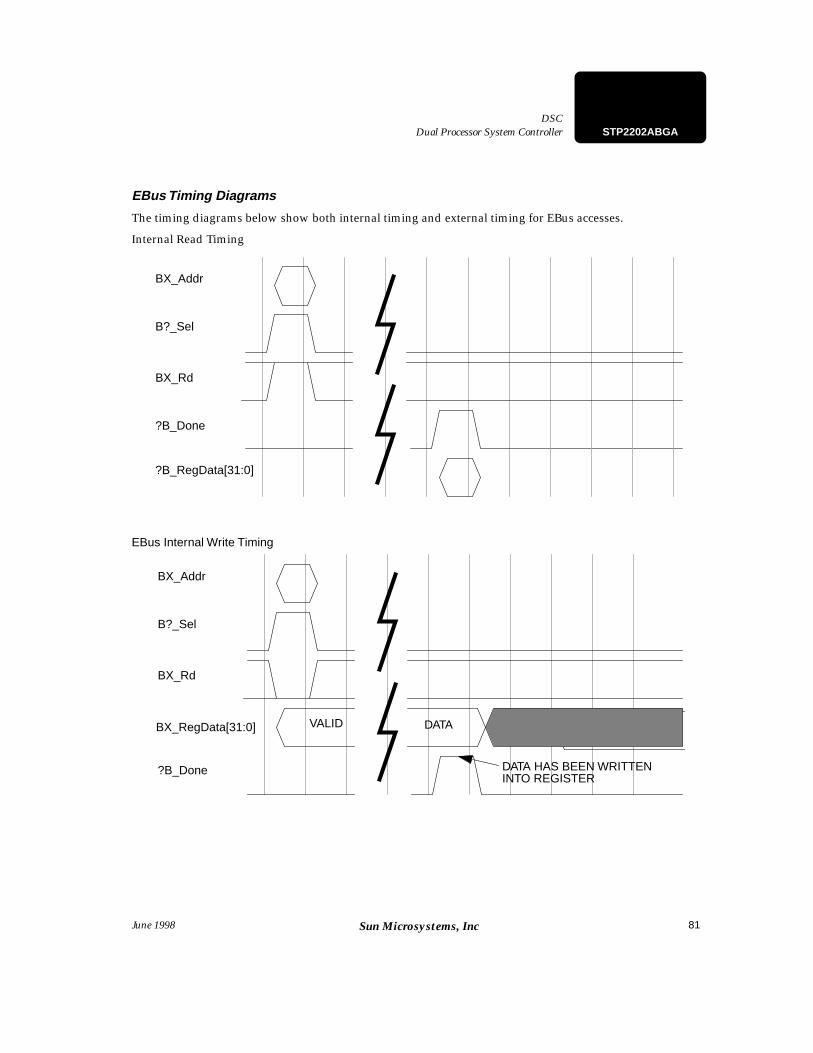
81
Dual Processor System ControllerDSC
STP2202ABGA
June 1998 Sun Microsystems, Inc
EBus Timing Diagrams
The timing diagrams below show both internal timing and external timing for EBus accesses.
Internal Read Timing
EBus Internal Write Timing
BX_Addr
B?_Sel
BX_Rd
?B_Done
?B_RegData[31:0]
BX_Addr
B?_Sel
BX_Rd
?B_Done
BX_RegData[31:0] VALID DATA
DATA HAS BEEN WRITTEN INTO REGISTER
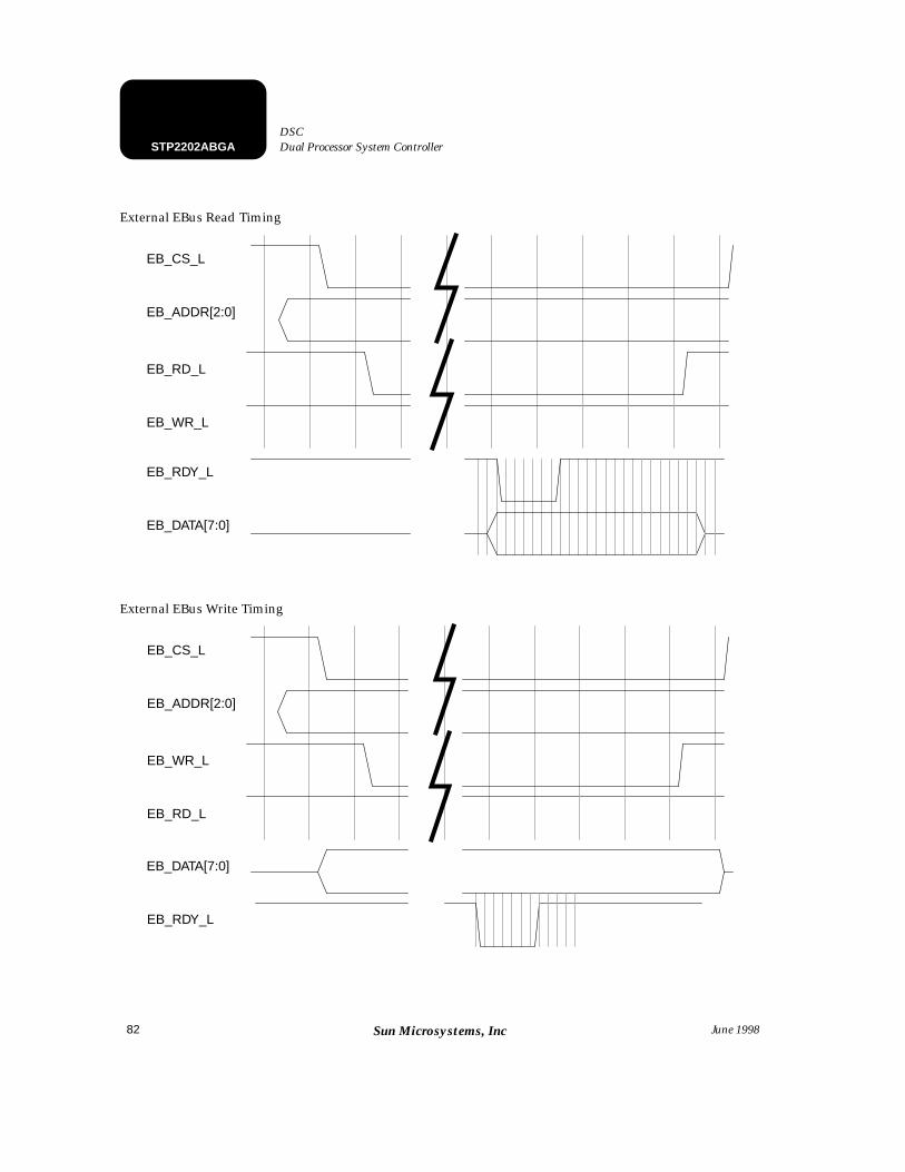
82
STP2202ABGA Dual Processor System Controller DSC
June 1998Sun Microsystems, Inc
External EBus Read Timing
External EBus Write Timing
EB_CS_L
EB_ADDR[2:0]
EB_RD_L
EB_WR_L
EB_RDY_L
EB_DATA[7:0]
EB_CS_L
EB_ADDR[2:0]
EB_WR_L
EB_RD_L
EB_RDY_L
EB_DATA[7:0]
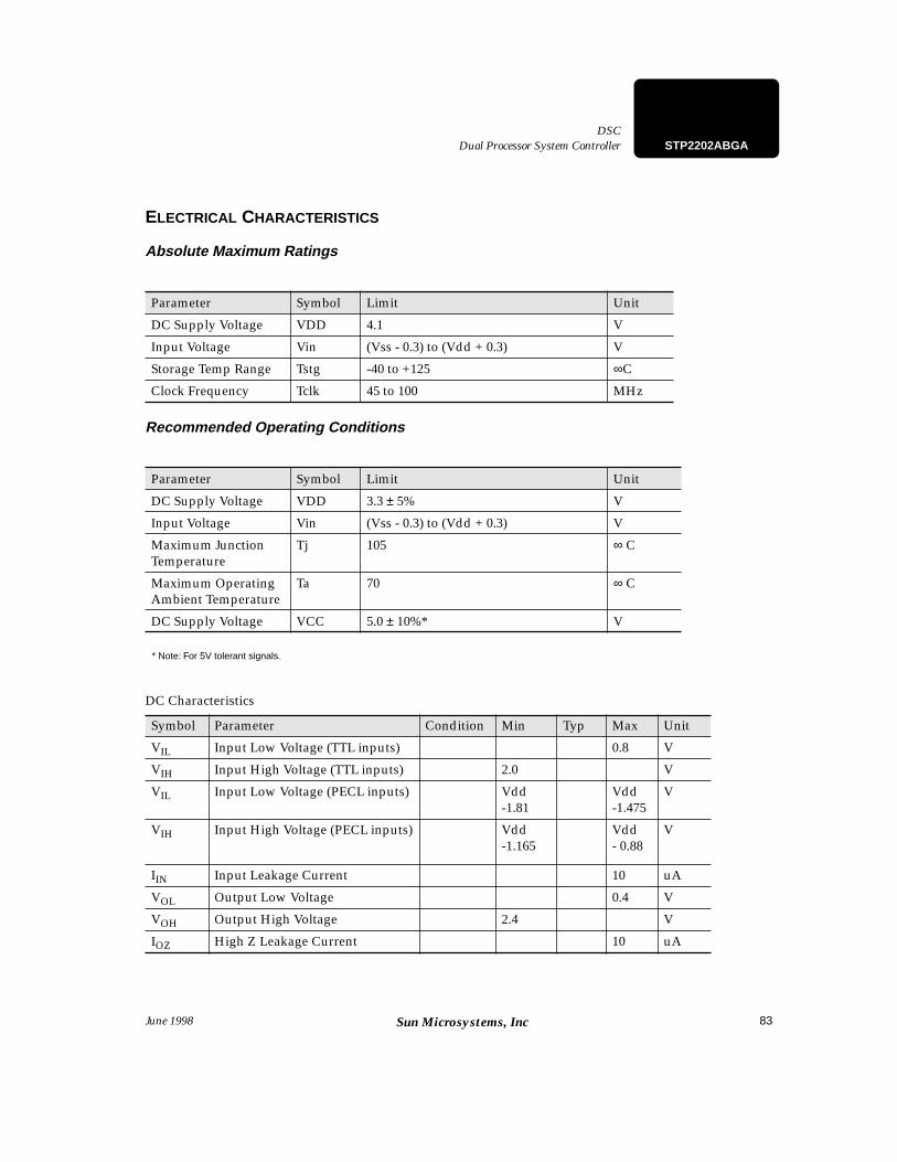
83
Dual Processor System ControllerDSC
STP2202ABGA
June 1998 Sun Microsystems, Inc
ELECTRICAL CHARACTERISTICS
Absolute Maximum Ratings
Recommended Operating Conditions
* Note: For 5V tolerant signals.
Parameter Symbol Limit Unit
DC Supply Voltage VDD 4.1 V
Input Voltage Vin (Vss - 0.3) to (Vdd + 0.3) V
Storage Temp Range Tstg -40 to +125 ∞C
Clock Frequency Tclk 45 to 100 MHz
Parameter Symbol Limit Unit
DC Supply Voltage VDD 3.3 ± 5% V
Input Voltage Vin (Vss - 0.3) to (Vdd + 0.3) V
Maximum Junction Temperature
Tj 105 ∞ C
Maximum Operating Ambient Temperature
Ta 70 ∞ C
DC Supply Voltage VCC 5.0 ± 10%* V
DC Characteristics
Symbol Parameter Condition Min Typ Max Unit
VIL Input Low Voltage (TTL inputs) 0.8 V
VIH Input High Voltage (TTL inputs) 2.0 V
VIL Input Low Voltage (PECL inputs) Vdd-1.81
Vdd-1.475
V
VIH Input High Voltage (PECL inputs) Vdd-1.165
Vdd- 0.88
V
IIN Input Leakage Current 10 uA
VOL Output Low Voltage 0.4 V
VOH Output High Voltage 2.4 V
IOZ High Z Leakage Current 10 uA
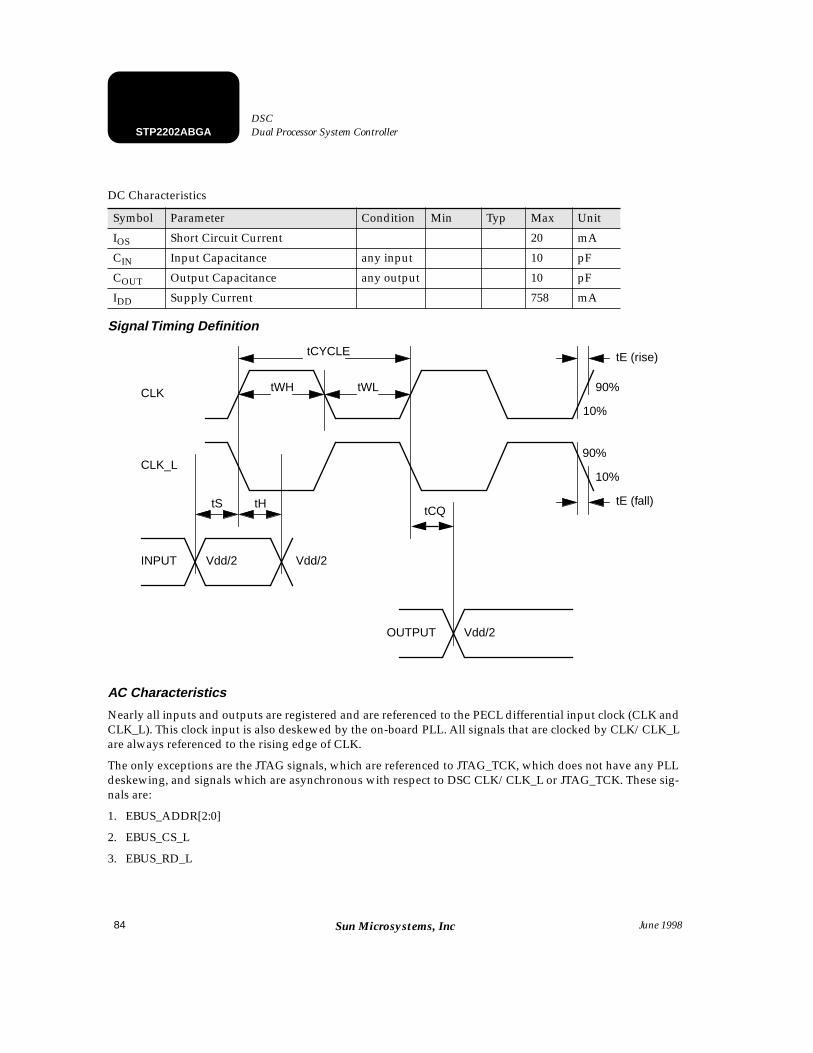
84
STP2202ABGA Dual Processor System Controller DSC
June 1998Sun Microsystems, Inc
Signal Timing Definition
AC Characteristics
Nearly all inputs and outputs are registered and are referenced to the PECL differential input clock (CLK and CLK_L). This clock input is also deskewed by the on-board PLL. All signals that are clocked by CLK/CLK_L are always referenced to the rising edge of CLK.
The only exceptions are the JTAG signals, which are referenced to JTAG_TCK, which does not have any PLL deskewing, and signals which are asynchronous with respect to DSC CLK/CLK_L or JTAG_TCK. These sig-nals are:
1. EBUS_ADDR[2:0]
2. EBUS_CS_L
3. EBUS_RD_L
IOS Short Circuit Current 20 mA
CIN Input Capacitance any input 10 pF
COUT Output Capacitance any output 10 pF
IDD Supply Current 758 mA
DC Characteristics
Symbol Parameter Condition Min Typ Max Unit
tCYCLE
tWH tWL
tCQtHtS
tE (rise)
tE (fall)
OUTPUT
INPUT
CLK
CLK_L
Vdd/2Vdd/2
Vdd/2
90%
90%
10%
10%
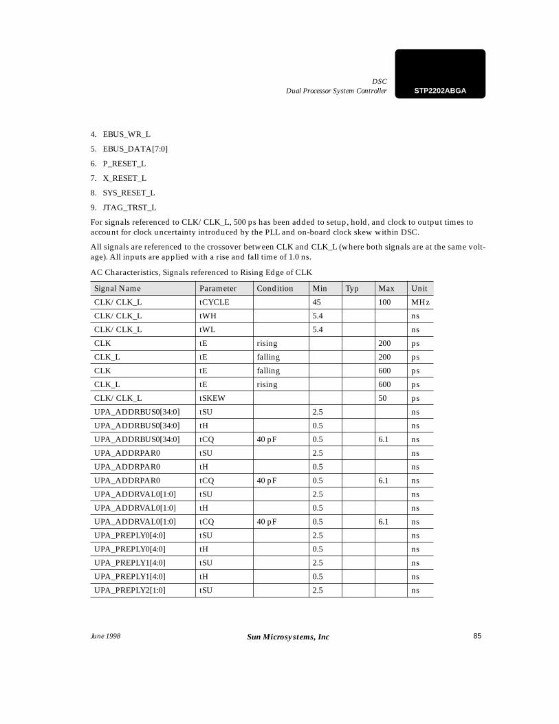
85
Dual Processor System ControllerDSC
STP2202ABGA
June 1998 Sun Microsystems, Inc
4. EBUS_WR_L
5. EBUS_DATA[7:0]
6. P_RESET_L
7. X_RESET_L
8. SYS_RESET_L
9. JTAG_TRST_L
For signals referenced to CLK/CLK_L, 500 ps has been added to setup, hold, and clock to output times to account for clock uncertainty introduced by the PLL and on-board clock skew within DSC.
All signals are referenced to the crossover between CLK and CLK_L (where both signals are at the same volt-age). All inputs are applied with a rise and fall time of 1.0 ns.
AC Characteristics, Signals referenced to Rising Edge of CLK
Signal Name Parameter Condition Min Typ Max Unit
CLK/CLK_L tCYCLE 45 100 MHz
CLK/CLK_L tWH 5.4 ns
CLK/CLK_L tWL 5.4 ns
CLK tE rising 200 ps
CLK_L tE falling 200 ps
CLK tE falling 600 ps
CLK_L tE rising 600 ps
CLK/CLK_L tSKEW 50 ps
UPA_ADDRBUS0[34:0] tSU 2.5 ns
UPA_ADDRBUS0[34:0] tH 0.5 ns
UPA_ADDRBUS0[34:0] tCQ 40 pF 0.5 6.1 ns
UPA_ADDRPAR0 tSU 2.5 ns
UPA_ADDRPAR0 tH 0.5 ns
UPA_ADDRPAR0 tCQ 40 pF 0.5 6.1 ns
UPA_ADDRVAL0[1:0] tSU 2.5 ns
UPA_ADDRVAL0[1:0] tH 0.5 ns
UPA_ADDRVAL0[1:0] tCQ 40 pF 0.5 6.1 ns
UPA_PREPLY0[4:0] tSU 2.5 ns
UPA_PREPLY0[4:0] tH 0.5 ns
UPA_PREPLY1[4:0] tSU 2.5 ns
UPA_PREPLY1[4:0] tH 0.5 ns
UPA_PREPLY2[1:0] tSU 2.5 ns
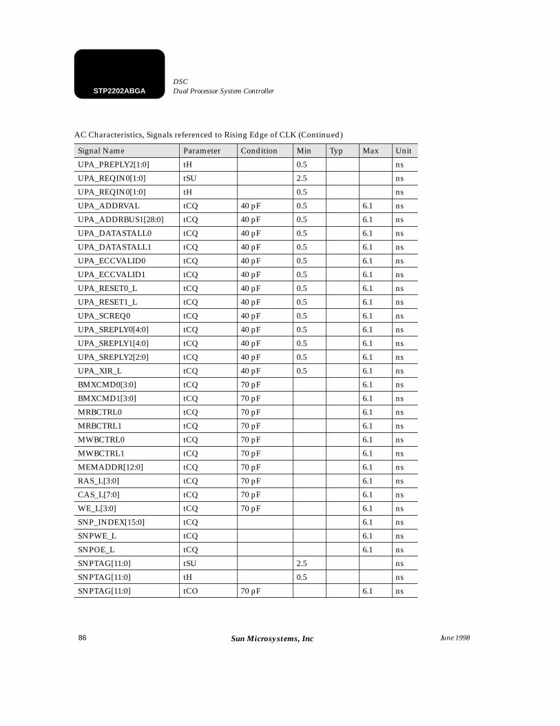
86
STP2202ABGA Dual Processor System Controller DSC
June 1998Sun Microsystems, Inc
UPA_PREPLY2[1:0] tH 0.5 ns
UPA_REQIN0[1:0] tSU 2.5 ns
UPA_REQIN0[1:0] tH 0.5 ns
UPA_ADDRVAL tCQ 40 pF 0.5 6.1 ns
UPA_ADDRBUS1[28:0] tCQ 40 pF 0.5 6.1 ns
UPA_DATASTALL0 tCQ 40 pF 0.5 6.1 ns
UPA_DATASTALL1 tCQ 40 pF 0.5 6.1 ns
UPA_ECCVALID0 tCQ 40 pF 0.5 6.1 ns
UPA_ECCVALID1 tCQ 40 pF 0.5 6.1 ns
UPA_RESET0_L tCQ 40 pF 0.5 6.1 ns
UPA_RESET1_L tCQ 40 pF 0.5 6.1 ns
UPA_SCREQ0 tCQ 40 pF 0.5 6.1 ns
UPA_SREPLY0[4:0] tCQ 40 pF 0.5 6.1 ns
UPA_SREPLY1[4:0] tCQ 40 pF 0.5 6.1 ns
UPA_SREPLY2[2:0] tCQ 40 pF 0.5 6.1 ns
UPA_XIR_L tCQ 40 pF 0.5 6.1 ns
BMXCMD0[3:0] tCQ 70 pF 6.1 ns
BMXCMD1[3:0] tCQ 70 pF 6.1 ns
MRBCTRL0 tCQ 70 pF 6.1 ns
MRBCTRL1 tCQ 70 pF 6.1 ns
MWBCTRL0 tCQ 70 pF 6.1 ns
MWBCTRL1 tCQ 70 pF 6.1 ns
MEMADDR[12:0] tCQ 70 pF 6.1 ns
RAS_L[3:0] tCQ 70 pF 6.1 ns
CAS_L[7:0] tCQ 70 pF 6.1 ns
WE_L[3:0] tCQ 70 pF 6.1 ns
SNP_INDEX[15:0] tCQ 6.1 ns
SNPWE_L tCQ 6.1 ns
SNPOE_L tCQ 6.1 ns
SNPTAG[11:0] tSU 2.5 ns
SNPTAG[11:0] tH 0.5 ns
SNPTAG[11:0] tCO 70 pF 6.1 ns
AC Characteristics, Signals referenced to Rising Edge of CLK (Continued)
Signal Name Parameter Condition Min Typ Max Unit
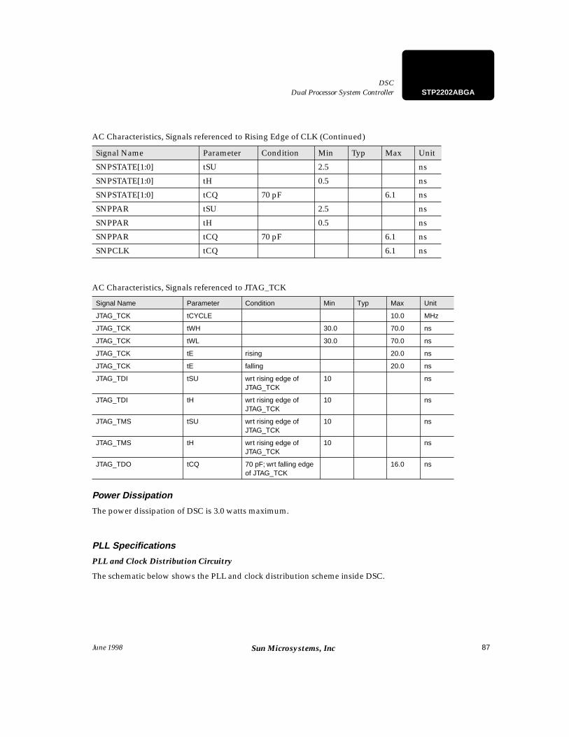
87
Dual Processor System ControllerDSC
STP2202ABGA
June 1998 Sun Microsystems, Inc
Power Dissipation
The power dissipation of DSC is 3.0 watts maximum.
PLL Specifications
PLL and Clock Distribution Circuitry
The schematic below shows the PLL and clock distribution scheme inside DSC.
SNPSTATE[1:0] tSU 2.5 ns
SNPSTATE[1:0] tH 0.5 ns
SNPSTATE[1:0] tCQ 70 pF 6.1 ns
SNPPAR tSU 2.5 ns
SNPPAR tH 0.5 ns
SNPPAR tCQ 70 pF 6.1 ns
SNPCLK tCQ 6.1 ns
AC Characteristics, Signals referenced to JTAG_TCK
Signal Name Parameter Condition Min Typ Max Unit
JTAG_TCK tCYCLE 10.0 MHz
JTAG_TCK tWH 30.0 70.0 ns
JTAG_TCK tWL 30.0 70.0 ns
JTAG_TCK tE rising 20.0 ns
JTAG_TCK tE falling 20.0 ns
JTAG_TDI tSU wrt rising edge of JTAG_TCK
10 ns
JTAG_TDI tH wrt rising edge of JTAG_TCK
10 ns
JTAG_TMS tSU wrt rising edge of JTAG_TCK
10 ns
JTAG_TMS tH wrt rising edge of JTAG_TCK
10 ns
JTAG_TDO tCQ 70 pF; wrt falling edge of JTAG_TCK
16.0 ns
AC Characteristics, Signals referenced to Rising Edge of CLK (Continued)
Signal Name Parameter Condition Min Typ Max Unit
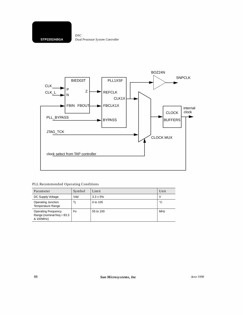
88
STP2202ABGA Dual Processor System Controller DSC
June 1998Sun Microsystems, Inc
PLL Recommended Operating Conditions
Parameter Symbol Limit Unit
DC Supply Voltage Vdd 3.3 ± 5% V
Operating Junction Temperature Range
Tj 0 to 105 °C
Operating Frequency Range (nominal freq = 83.3 & 100MHz)
Fo 55 to 100 MHz
P
N
FBIN FBOUT
Z
BIED03T
REFCLK
FBCLK1X
BYPASS
CLK1X
PLL1XSF
CLK
CLK_L
PLL_BYPASS
JTAG_TCK
clock select from TAP controller
CLOCK MUX
CLOCK
BUFFERS
internalclock
SNPCLK
BOZ24N
89
Dual Processor System ControllerDSC
STP2202ABGA
June 1998 Sun Microsystems, Inc
Mechanical Information
Pad Ring Assignments
Pad ring numbers and their associated ball numbers are shown below.
PLL DC Characteristics
Symbol Parameter Min Typ Max Unit
VIL LVTTL low - BYPASS
0.8 V
VIH LVTTL high- BYPASS
2.0 V
VIL LVPECL low - PECL CLK IN
Vdd - 1.810
Vdd -1.475
V
VIH LVPECL high - PECL CLK IN
Vdd -1.165
Vdd -0.88
V
PECL LVPECL rise and fall times
0.2 0.6 ns
PLL AC Characteristics
Parameter Min Typ Max Unit
Total jitter and clock skew over operation range.
-500 +500 ps
Prop delay during BYPSSS mode tbd tbd ns
Initial Startup time 250 us
Transition Startup time (from bypass to normal mode)
250 us
Output Duty Cycle 45 55 %
Output loading 300 pf
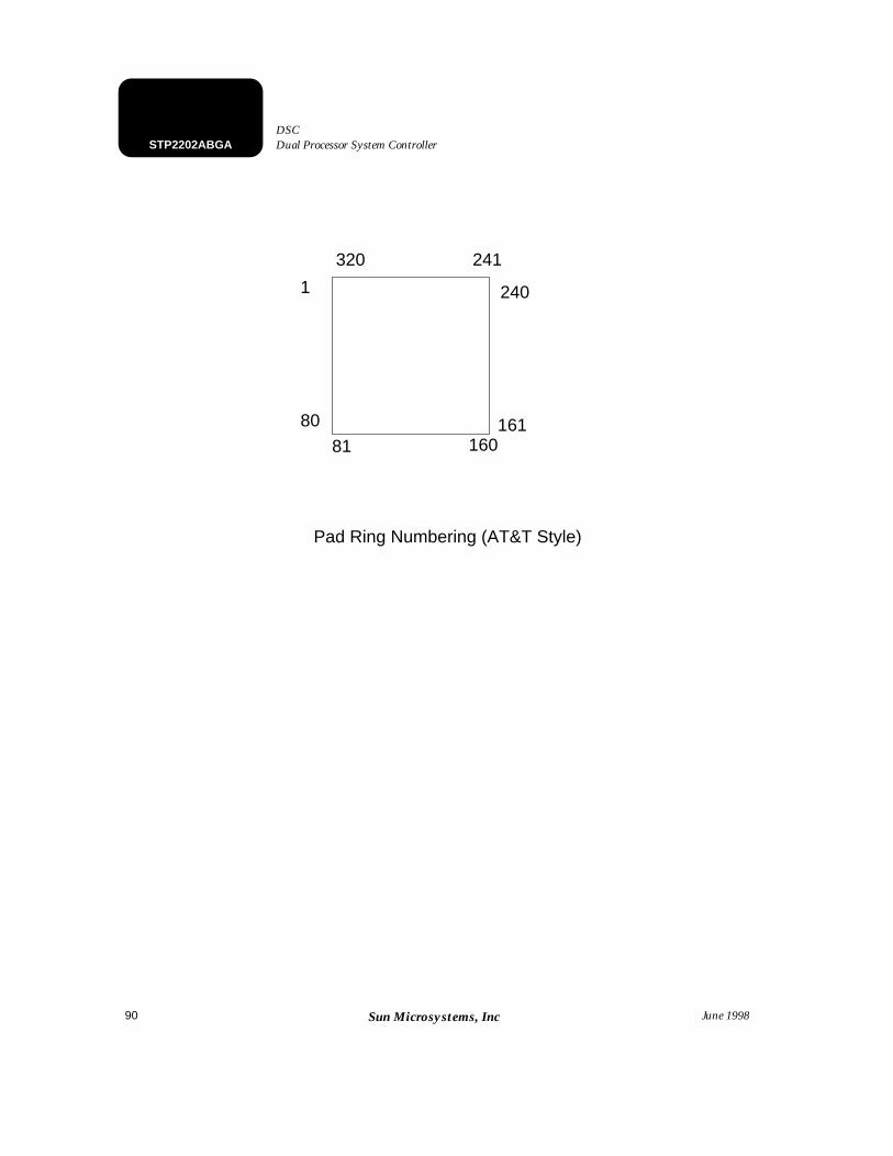
90
STP2202ABGA Dual Processor System Controller DSC
June 1998Sun Microsystems, Inc
320 241
240
16116081
80
1
Pad Ring Numbering (AT&T Style)
91
Dual Processor System ControllerDSC
STP2202ABGA
June 1998 Sun Microsystems, Inc
Figure 63. Footprint (Bottom View)
Y W V U T R P N M L K J H G F E D C B A
1
2
3
20
19
18
17
16
15
14
13
12
11
10
9
8
7
6
5
4
Y W V U T R P N M L K J H G F E D C B A
1
2
3
20
19
18
17
16
15
14
13
12
11
10
9
8
7
6
5
4
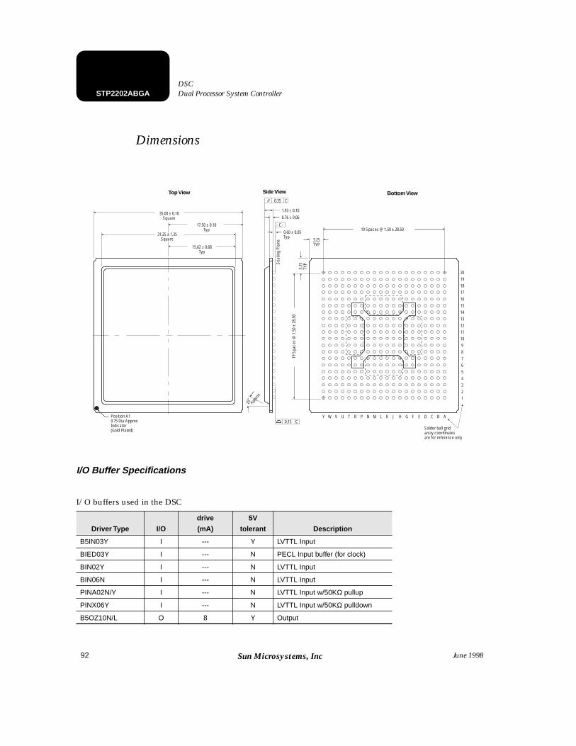
92
STP2202ABGA Dual Processor System Controller DSC
June 1998Sun Microsystems, Inc
Dimensions
I/O Buffer Specifications
I/O buffers used in the DSC
Driver Type I/O
drive
(mA)
5V
tolerant Description
B5IN03Y I --- Y LVTTL Input
BIED03Y I --- N PECL Input buffer (for clock)
BIN02Y I --- N LVTTL Input
BIN06N I --- N LVTTL Input
PINA02N/Y I --- N LVTTL Input w/50KΩ pullup
PINX06Y I --- N LVTTL Input w/50KΩ pulldown
B5OZ10N/L O 8 Y Output
Top View Side View
0.15 CPosition A10.75 Dia ApproxIndicator(Gold Plated)
25°
Appro
x
Solder ball gridarray coordinatesare for reference only
WY
19 S
pace
s @
1.5
0 ±
28.5
0
Seat
ing
Plan
e
19 Spaces @ 1.50 ± 28.50
3.25
TYP
3.25TYP15.62 ± 0.68
Typ
17.50 ± 0.10Typ
31.25 ± 1.35Square
35.00 ± 0.10Square
0.60 ± 0.05Typ
1.93 ± 0.100.76 ± 0.06
- C -
C// 0.35
V U T R P N M L K J H G F E D C B A
2019181716151413121110987654321
Bottom View
93
Dual Processor System ControllerDSC
STP2202ABGA
June 1998 Sun Microsystems, Inc
Note that buffers with the suffix N, L or Y in the driver type will have identical function, but the die layout will be slightly different.
BON10Y O 10 N Output
BOZ24N/L/Y O 24 N Output
BN02Z24N/L/Y I/O 24/24 N Bidirectional, no bus-hold
B5N3Z10Y I/O 10/8 Y Bidirectional, no bus-hold
P4OZ24N/Y I/O 24/24 N Bidirectional, no bus-hold.Tuned for driving transmission line load
I/O buffers used in the DSC
Driver Type I/O
drive
(mA)
5V
tolerant Description
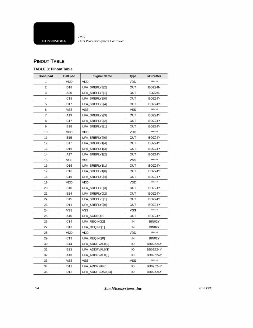
94
STP2202ABGA Dual Processor System Controller DSC
June 1998Sun Microsystems, Inc
PINOUT TABLE
TABLE 3: Pinout Table
Bond pad Ball pad Signal Name Type I/O buffer
1 VDD VDD VDD ******
2 D18 UPA_SREPLY3[2] OUT BOZ24N
3 A20 UPA_SREPLY3[1] OUT BOZ24L
4 C18 UPA_SREPLY3[0] OUT BOZ24Y
5 D17 UPA_SREPLY2[4] OUT BOZ24Y
6 VSS VSS VSS ******
7 A19 UPA_SREPLY2[3] OUT BOZ24Y
8 C17 UPA_SREPLY2[2] OUT BOZ24Y
9 B18 UPA_SREPLY2[1] OUT BOZ24Y
10 VDD VDD VDD ******
11 E15 UPA_SREPLY2[0] OUT BOZ24Y
12 B17 UPA_SREPLY1[4] OUT BOZ24Y
13 D16 UPA_SREPLY1[3] OUT BOZ24Y
14 A17 UPA_SREPLY1[2] OUT BOZ24Y
15 VSS VSS VSS ******
16 D15 UPA_SREPLY1[1] OUT BOZ24Y
17 C16 UPA_SREPLY1[0] OUT BOZ24Y
18 C15 UPA_SREPLY0[4] OUT BOZ24Y
19 VDD VDD VDD ******
20 B16 UPA_SREPLY0[3] OUT BOZ24Y
21 E14 UPA_SREPLY0[2] OUT BOZ24Y
22 B15 UPA_SREPLY0[1] OUT BOZ24Y
23 D14 UPA_SREPLY0[0] OUT BOZ24Y
24 VSS VSS VSS ******
25 A15 UPA_SCREQ00 OUT BOZ24Y
26 C14 UPA_REQIN0[2] IN BIN02Y
27 D13 UPA_REQIN0[1] IN BIN02Y
28 VDD VDD VDD ******
29 C13 UPA_REQIN0[0] IN BIN02Y
30 B14 UPA_ADDRVAL0[2] IO BB02Z24Y
31 B13 UPA_ADDRVAL0[1] IO BB02Z24Y
32 A13 UPA_ADDRVAL0[0] IO BB02Z24Y
33 VSS VSS VSS ******
34 D11 UPA_ADDRPAR0 IO BB02Z24Y
35 D12 UPA_ADDRBUS0[34] IO BB02Z24Y
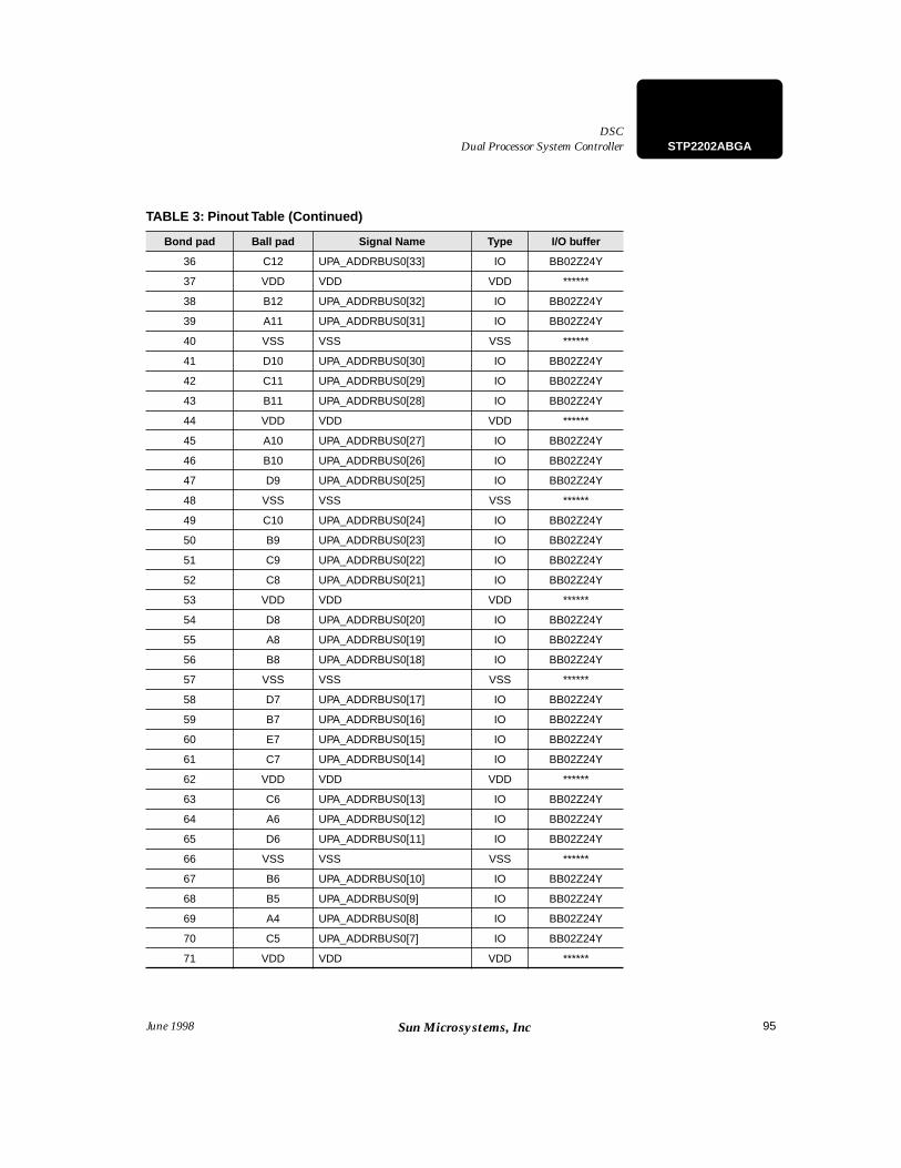
95
Dual Processor System ControllerDSC
STP2202ABGA
June 1998 Sun Microsystems, Inc
36 C12 UPA_ADDRBUS0[33] IO BB02Z24Y
37 VDD VDD VDD ******
38 B12 UPA_ADDRBUS0[32] IO BB02Z24Y
39 A11 UPA_ADDRBUS0[31] IO BB02Z24Y
40 VSS VSS VSS ******
41 D10 UPA_ADDRBUS0[30] IO BB02Z24Y
42 C11 UPA_ADDRBUS0[29] IO BB02Z24Y
43 B11 UPA_ADDRBUS0[28] IO BB02Z24Y
44 VDD VDD VDD ******
45 A10 UPA_ADDRBUS0[27] IO BB02Z24Y
46 B10 UPA_ADDRBUS0[26] IO BB02Z24Y
47 D9 UPA_ADDRBUS0[25] IO BB02Z24Y
48 VSS VSS VSS ******
49 C10 UPA_ADDRBUS0[24] IO BB02Z24Y
50 B9 UPA_ADDRBUS0[23] IO BB02Z24Y
51 C9 UPA_ADDRBUS0[22] IO BB02Z24Y
52 C8 UPA_ADDRBUS0[21] IO BB02Z24Y
53 VDD VDD VDD ******
54 D8 UPA_ADDRBUS0[20] IO BB02Z24Y
55 A8 UPA_ADDRBUS0[19] IO BB02Z24Y
56 B8 UPA_ADDRBUS0[18] IO BB02Z24Y
57 VSS VSS VSS ******
58 D7 UPA_ADDRBUS0[17] IO BB02Z24Y
59 B7 UPA_ADDRBUS0[16] IO BB02Z24Y
60 E7 UPA_ADDRBUS0[15] IO BB02Z24Y
61 C7 UPA_ADDRBUS0[14] IO BB02Z24Y
62 VDD VDD VDD ******
63 C6 UPA_ADDRBUS0[13] IO BB02Z24Y
64 A6 UPA_ADDRBUS0[12] IO BB02Z24Y
65 D6 UPA_ADDRBUS0[11] IO BB02Z24Y
66 VSS VSS VSS ******
67 B6 UPA_ADDRBUS0[10] IO BB02Z24Y
68 B5 UPA_ADDRBUS0[9] IO BB02Z24Y
69 A4 UPA_ADDRBUS0[8] IO BB02Z24Y
70 C5 UPA_ADDRBUS0[7] IO BB02Z24Y
71 VDD VDD VDD ******
TABLE 3: Pinout Table (Continued)
Bond pad Ball pad Signal Name Type I/O buffer
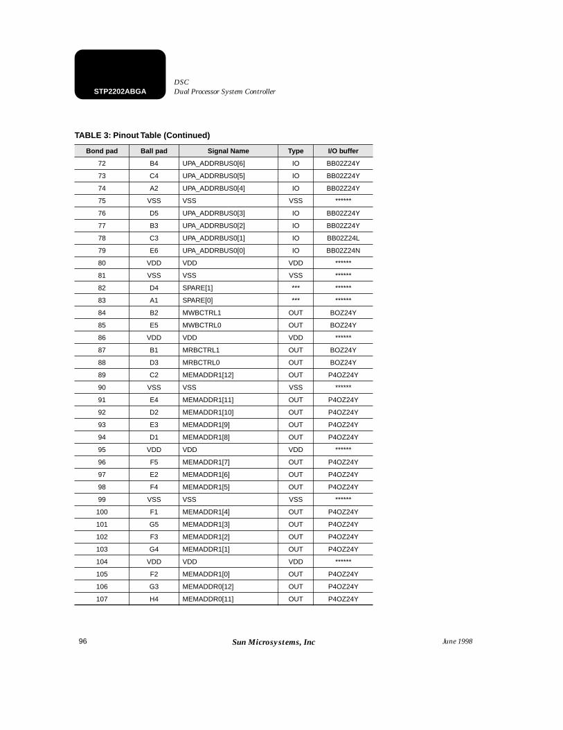
96
STP2202ABGA Dual Processor System Controller DSC
June 1998Sun Microsystems, Inc
72 B4 UPA_ADDRBUS0[6] IO BB02Z24Y
73 C4 UPA_ADDRBUS0[5] IO BB02Z24Y
74 A2 UPA_ADDRBUS0[4] IO BB02Z24Y
75 VSS VSS VSS ******
76 D5 UPA_ADDRBUS0[3] IO BB02Z24Y
77 B3 UPA_ADDRBUS0[2] IO BB02Z24Y
78 C3 UPA_ADDRBUS0[1] IO BB02Z24L
79 E6 UPA_ADDRBUS0[0] IO BB02Z24N
80 VDD VDD VDD ******
81 VSS VSS VSS ******
82 D4 SPARE[1] *** ******
83 A1 SPARE[0] *** ******
84 B2 MWBCTRL1 OUT BOZ24Y
85 E5 MWBCTRL0 OUT BOZ24Y
86 VDD VDD VDD ******
87 B1 MRBCTRL1 OUT BOZ24Y
88 D3 MRBCTRL0 OUT BOZ24Y
89 C2 MEMADDR1[12] OUT P4OZ24Y
90 VSS VSS VSS ******
91 E4 MEMADDR1[11] OUT P4OZ24Y
92 D2 MEMADDR1[10] OUT P4OZ24Y
93 E3 MEMADDR1[9] OUT P4OZ24Y
94 D1 MEMADDR1[8] OUT P4OZ24Y
95 VDD VDD VDD ******
96 F5 MEMADDR1[7] OUT P4OZ24Y
97 E2 MEMADDR1[6] OUT P4OZ24Y
98 F4 MEMADDR1[5] OUT P4OZ24Y
99 VSS VSS VSS ******
100 F1 MEMADDR1[4] OUT P4OZ24Y
101 G5 MEMADDR1[3] OUT P4OZ24Y
102 F3 MEMADDR1[2] OUT P4OZ24Y
103 G4 MEMADDR1[1] OUT P4OZ24Y
104 VDD VDD VDD ******
105 F2 MEMADDR1[0] OUT P4OZ24Y
106 G3 MEMADDR0[12] OUT P4OZ24Y
107 H4 MEMADDR0[11] OUT P4OZ24Y
TABLE 3: Pinout Table (Continued)
Bond pad Ball pad Signal Name Type I/O buffer
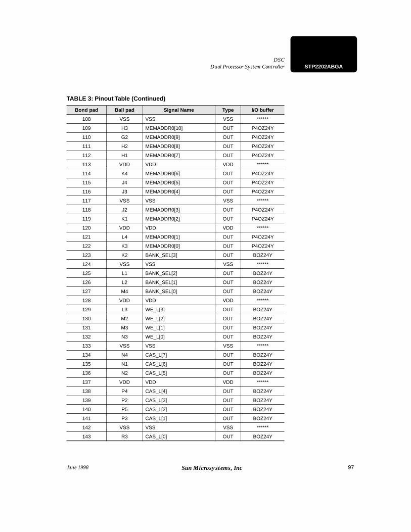
97
Dual Processor System ControllerDSC
STP2202ABGA
June 1998 Sun Microsystems, Inc
108 VSS VSS VSS ******
109 H3 MEMADDR0[10] OUT P4OZ24Y
110 G2 MEMADDR0[9] OUT P4OZ24Y
111 H2 MEMADDR0[8] OUT P4OZ24Y
112 H1 MEMADDR0[7] OUT P4OZ24Y
113 VDD VDD VDD ******
114 K4 MEMADDR0[6] OUT P4OZ24Y
115 J4 MEMADDR0[5] OUT P4OZ24Y
116 J3 MEMADDR0[4] OUT P4OZ24Y
117 VSS VSS VSS ******
118 J2 MEMADDR0[3] OUT P4OZ24Y
119 K1 MEMADDR0[2] OUT P4OZ24Y
120 VDD VDD VDD ******
121 L4 MEMADDR0[1] OUT P4OZ24Y
122 K3 MEMADDR0[0] OUT P4OZ24Y
123 K2 BANK_SEL[3] OUT BOZ24Y
124 VSS VSS VSS ******
125 L1 BANK_SEL[2] OUT BOZ24Y
126 L2 BANK_SEL[1] OUT BOZ24Y
127 M4 BANK_SEL[0] OUT BOZ24Y
128 VDD VDD VDD ******
129 L3 WE_L[3] OUT BOZ24Y
130 M2 WE_L[2] OUT BOZ24Y
131 M3 WE_L[1] OUT BOZ24Y
132 N3 WE_L[0] OUT BOZ24Y
133 VSS VSS VSS ******
134 N4 CAS_L[7] OUT BOZ24Y
135 N1 CAS_L[6] OUT BOZ24Y
136 N2 CAS_L[5] OUT BOZ24Y
137 VDD VDD VDD ******
138 P4 CAS_L[4] OUT BOZ24Y
139 P2 CAS_L[3] OUT BOZ24Y
140 P5 CAS_L[2] OUT BOZ24Y
141 P3 CAS_L[1] OUT BOZ24Y
142 VSS VSS VSS ******
143 R3 CAS_L[0] OUT BOZ24Y
TABLE 3: Pinout Table (Continued)
Bond pad Ball pad Signal Name Type I/O buffer
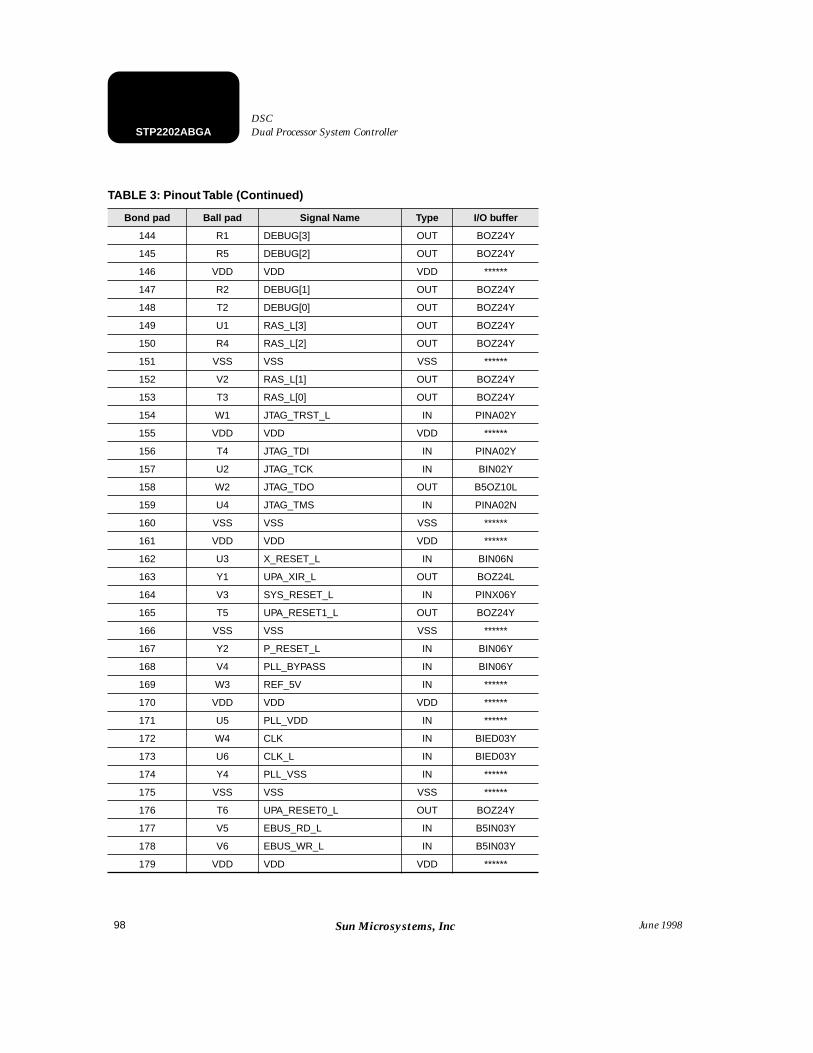
98
STP2202ABGA Dual Processor System Controller DSC
June 1998Sun Microsystems, Inc
144 R1 DEBUG[3] OUT BOZ24Y
145 R5 DEBUG[2] OUT BOZ24Y
146 VDD VDD VDD ******
147 R2 DEBUG[1] OUT BOZ24Y
148 T2 DEBUG[0] OUT BOZ24Y
149 U1 RAS_L[3] OUT BOZ24Y
150 R4 RAS_L[2] OUT BOZ24Y
151 VSS VSS VSS ******
152 V2 RAS_L[1] OUT BOZ24Y
153 T3 RAS_L[0] OUT BOZ24Y
154 W1 JTAG_TRST_L IN PINA02Y
155 VDD VDD VDD ******
156 T4 JTAG_TDI IN PINA02Y
157 U2 JTAG_TCK IN BIN02Y
158 W2 JTAG_TDO OUT B5OZ10L
159 U4 JTAG_TMS IN PINA02N
160 VSS VSS VSS ******
161 VDD VDD VDD ******
162 U3 X_RESET_L IN BIN06N
163 Y1 UPA_XIR_L OUT BOZ24L
164 V3 SYS_RESET_L IN PINX06Y
165 T5 UPA_RESET1_L OUT BOZ24Y
166 VSS VSS VSS ******
167 Y2 P_RESET_L IN BIN06Y
168 V4 PLL_BYPASS IN BIN06Y
169 W3 REF_5V IN ******
170 VDD VDD VDD ******
171 U5 PLL_VDD IN ******
172 W4 CLK IN BIED03Y
173 U6 CLK_L IN BIED03Y
174 Y4 PLL_VSS IN ******
175 VSS VSS VSS ******
176 T6 UPA_RESET0_L OUT BOZ24Y
177 V5 EBUS_RD_L IN B5IN03Y
178 V6 EBUS_WR_L IN B5IN03Y
179 VDD VDD VDD ******
TABLE 3: Pinout Table (Continued)
Bond pad Ball pad Signal Name Type I/O buffer
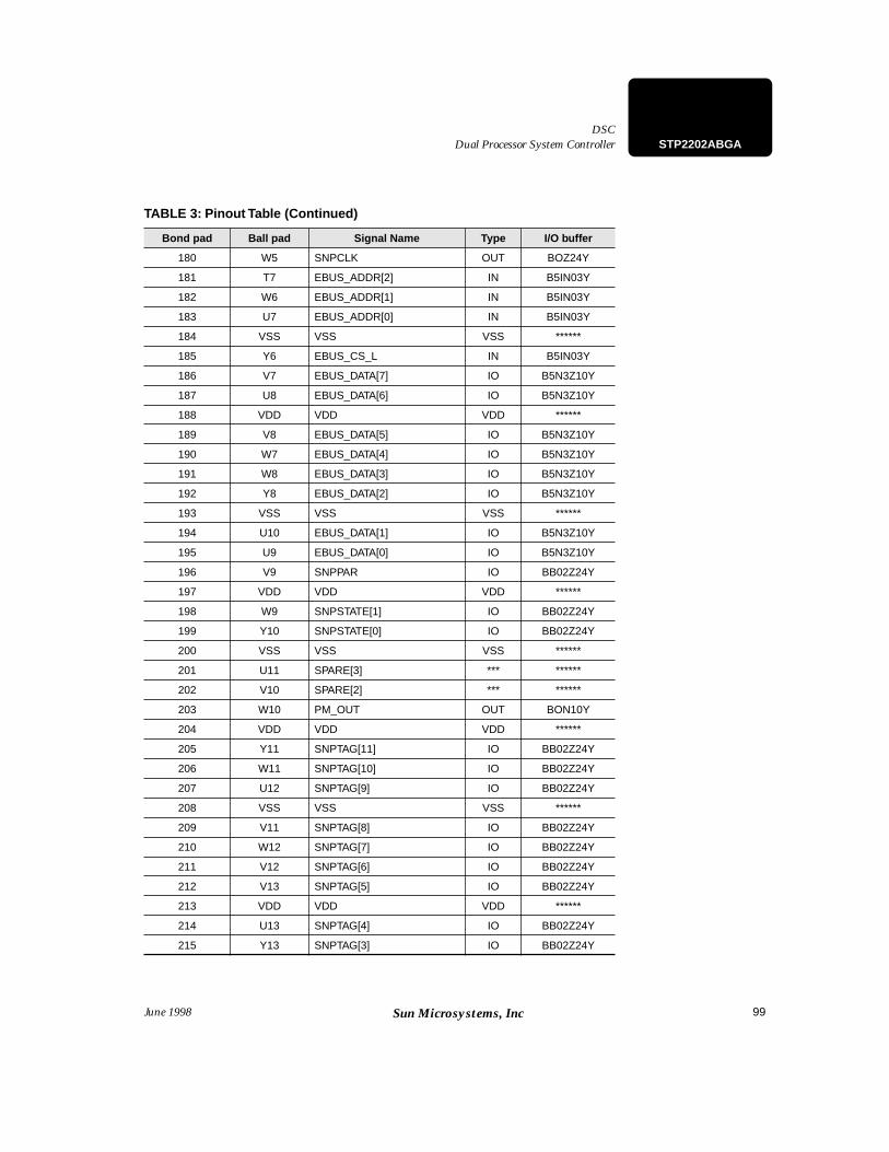
99
Dual Processor System ControllerDSC
STP2202ABGA
June 1998 Sun Microsystems, Inc
180 W5 SNPCLK OUT BOZ24Y
181 T7 EBUS_ADDR[2] IN B5IN03Y
182 W6 EBUS_ADDR[1] IN B5IN03Y
183 U7 EBUS_ADDR[0] IN B5IN03Y
184 VSS VSS VSS ******
185 Y6 EBUS_CS_L IN B5IN03Y
186 V7 EBUS_DATA[7] IO B5N3Z10Y
187 U8 EBUS_DATA[6] IO B5N3Z10Y
188 VDD VDD VDD ******
189 V8 EBUS_DATA[5] IO B5N3Z10Y
190 W7 EBUS_DATA[4] IO B5N3Z10Y
191 W8 EBUS_DATA[3] IO B5N3Z10Y
192 Y8 EBUS_DATA[2] IO B5N3Z10Y
193 VSS VSS VSS ******
194 U10 EBUS_DATA[1] IO B5N3Z10Y
195 U9 EBUS_DATA[0] IO B5N3Z10Y
196 V9 SNPPAR IO BB02Z24Y
197 VDD VDD VDD ******
198 W9 SNPSTATE[1] IO BB02Z24Y
199 Y10 SNPSTATE[0] IO BB02Z24Y
200 VSS VSS VSS ******
201 U11 SPARE[3] *** ******
202 V10 SPARE[2] *** ******
203 W10 PM_OUT OUT BON10Y
204 VDD VDD VDD ******
205 Y11 SNPTAG[11] IO BB02Z24Y
206 W11 SNPTAG[10] IO BB02Z24Y
207 U12 SNPTAG[9] IO BB02Z24Y
208 VSS VSS VSS ******
209 V11 SNPTAG[8] IO BB02Z24Y
210 W12 SNPTAG[7] IO BB02Z24Y
211 V12 SNPTAG[6] IO BB02Z24Y
212 V13 SNPTAG[5] IO BB02Z24Y
213 VDD VDD VDD ******
214 U13 SNPTAG[4] IO BB02Z24Y
215 Y13 SNPTAG[3] IO BB02Z24Y
TABLE 3: Pinout Table (Continued)
Bond pad Ball pad Signal Name Type I/O buffer
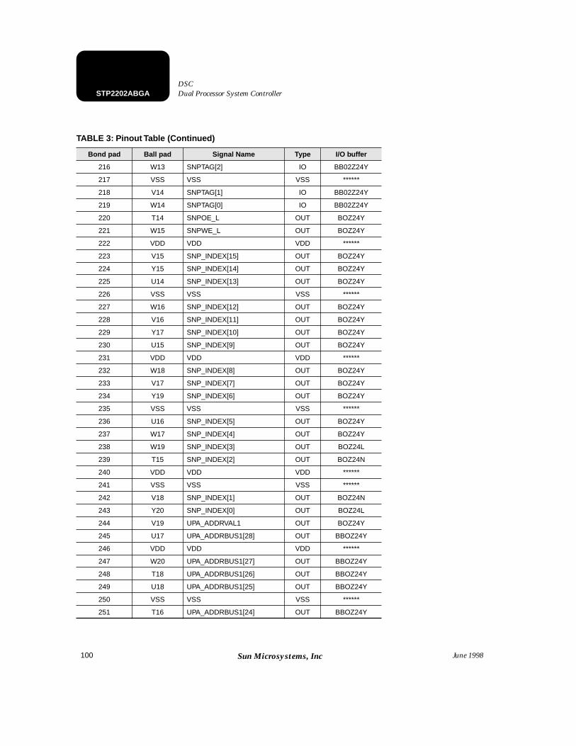
100
STP2202ABGA Dual Processor System Controller DSC
June 1998Sun Microsystems, Inc
216 W13 SNPTAG[2] IO BB02Z24Y
217 VSS VSS VSS ******
218 V14 SNPTAG[1] IO BB02Z24Y
219 W14 SNPTAG[0] IO BB02Z24Y
220 T14 SNPOE_L OUT BOZ24Y
221 W15 SNPWE_L OUT BOZ24Y
222 VDD VDD VDD ******
223 V15 SNP_INDEX[15] OUT BOZ24Y
224 Y15 SNP_INDEX[14] OUT BOZ24Y
225 U14 SNP_INDEX[13] OUT BOZ24Y
226 VSS VSS VSS ******
227 W16 SNP_INDEX[12] OUT BOZ24Y
228 V16 SNP_INDEX[11] OUT BOZ24Y
229 Y17 SNP_INDEX[10] OUT BOZ24Y
230 U15 SNP_INDEX[9] OUT BOZ24Y
231 VDD VDD VDD ******
232 W18 SNP_INDEX[8] OUT BOZ24Y
233 V17 SNP_INDEX[7] OUT BOZ24Y
234 Y19 SNP_INDEX[6] OUT BOZ24Y
235 VSS VSS VSS ******
236 U16 SNP_INDEX[5] OUT BOZ24Y
237 W17 SNP_INDEX[4] OUT BOZ24Y
238 W19 SNP_INDEX[3] OUT BOZ24L
239 T15 SNP_INDEX[2] OUT BOZ24N
240 VDD VDD VDD ******
241 VSS VSS VSS ******
242 V18 SNP_INDEX[1] OUT BOZ24N
243 Y20 SNP_INDEX[0] OUT BOZ24L
244 V19 UPA_ADDRVAL1 OUT BOZ24Y
245 U17 UPA_ADDRBUS1[28] OUT BBOZ24Y
246 VDD VDD VDD ******
247 W20 UPA_ADDRBUS1[27] OUT BBOZ24Y
248 T18 UPA_ADDRBUS1[26] OUT BBOZ24Y
249 U18 UPA_ADDRBUS1[25] OUT BBOZ24Y
250 VSS VSS VSS ******
251 T16 UPA_ADDRBUS1[24] OUT BBOZ24Y
TABLE 3: Pinout Table (Continued)
Bond pad Ball pad Signal Name Type I/O buffer
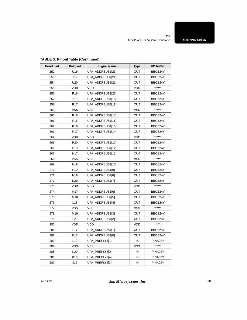
101
Dual Processor System ControllerDSC
STP2202ABGA
June 1998 Sun Microsystems, Inc
252 U19 UPA_ADDRBUS1[23] OUT BBOZ24Y
253 T17 UPA_ADDRBUS1[22] OUT BBOZ24Y
254 U20 UPA_ADDRBUS1[21] OUT BBOZ24Y
255 VDD VDD VDD ******
256 R16 UPA_ADDRBUS1[20] OUT BBOZ24Y
257 T19 UPA_ADDRBUS1[19] OUT BBOZ24Y
258 R17 UPA_ADDRBUS1[18] OUT BBOZ24Y
259 VSS VSS VSS ******
260 R19 UPA_ADDRBUS1[17] OUT BBOZ24Y
261 P16 UPA_ADDRBUS1[16] OUT BBOZ24Y
262 R18 UPA_ADDRBUS1[15] OUT BBOZ24Y
263 P17 UPA_ADDRBUS1[14] OUT BBOZ24Y
264 VDD VDD VDD ******
265 R20 UPA_ADDRBUS1[13] OUT BBOZ24Y
266 P18 UPA_ADDRBUS1[12] OUT BBOZ24Y
267 N17 UPA_ADDRBUS1[11] OUT BBOZ24Y
268 VSS VSS VSS ******
269 N18 UPA_ADDRBUS1[10] OUT BBOZ24Y
270 P19 UPA_ADDRBUS1[9] OUT BBOZ24Y
271 N19 UPA_ADDRBUS1[8] OUT BBOZ24Y
272 N20 UPA_ADDRBUS1[7] OUT BBOZ24Y
273 VDD VDD VDD ******
274 M17 UPA_ADDRBUS1[6] OUT BBOZ24Y
275 M18 UPA_ADDRBUS1[5] OUT BBOZ24Y
276 L18 UPA_ADDRBUS1[4] OUT BBOZ24Y
277 VSS VSS VSS ******
278 M19 UPA_ADDRBUS1[3] OUT BBOZ24Y
279 L20 UPA_ADDRBUS1[2] OUT BBOZ24Y
280 VDD VDD VDD ******
281 L17 UPA_ADDRBUS1[1] OUT BBOZ24Y
282 K17 UPA_ADDRBUS1[0] OUT BBOZ24Y
283 L19 UPA_PREPLY3[1] IN PINA02Y
284 VSS VSS VSS ******
285 K20 UPA_PREPLY3[0] IN PINA02Y
286 K19 UPA_PREPLY2[4] IN PINA02Y
287 J17 UPA_PREPLY2[3] IN PINA02Y
TABLE 3: Pinout Table (Continued)
Bond pad Ball pad Signal Name Type I/O buffer
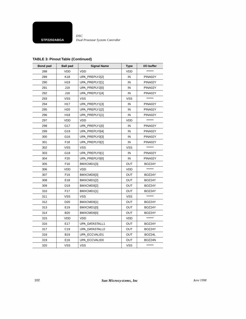
102
STP2202ABGA Dual Processor System Controller DSC
June 1998Sun Microsystems, Inc
288 VDD VDD VDD ******
289 K18 UPA_PREPLY2[2] IN PINA02Y
290 H19 UPA_PREPLY2[1] IN PINA02Y
291 J19 UPA_PREPLY2[0] IN PINA02Y
292 J18 UPA_PREPLY1[4] IN PINA02Y
293 VSS VSS VSS ******
294 H17 UPA_PREPLY1[3] IN PINA02Y
295 H20 UPA_PREPLY1[2] IN PINA02Y
296 H18 UPA_PREPLY1[1] IN PINA02Y
297 VDD VDD VDD ******
298 G17 UPA_PREPLY1[0] IN PINA02Y
299 G19 UPA_PREPLY0[4] IN PINA02Y
300 G16 UPA_PREPLY0[3] IN PINA02Y
301 F18 UPA_PREPLY0[2] IN PINA02Y
302 VSS VSS VSS ******
303 G18 UPA_PREPLY0[1] IN PINA02Y
304 F20 UPA_PREPLY0[0] IN PINA02Y
305 F16 BMXCMD1[3] OUT BOZ24Y
306 VDD VDD VDD ******
307 F19 BMXCMD0[3] OUT BOZ24Y
308 E18 BMXCMD1[2] OUT BOZ24Y
309 D19 BMXCMD0[2] OUT BOZ24Y
310 F17 BMXCMD1[1] OUT BOZ24Y
311 VSS VSS VSS ******
312 D20 BMXCMD0[1] OUT BOZ24Y
313 E19 BMXCMD1[0] OUT BOZ24Y
314 B20 BMXCMD0[0] OUT BOZ24Y
315 VDD VDD VDD ******
316 E17 UPA_DATASTALL1 OUT BOZ24Y
317 C19 UPA_DATASTALL0 OUT BOZ24Y
318 B19 UPA_ECCVALID1 OUT BOZ24L
319 E16 UPA_ECCVALID0 OUT BOZ24N
320 VSS VSS VSS ******
TABLE 3: Pinout Table (Continued)
Bond pad Ball pad Signal Name Type I/O buffer
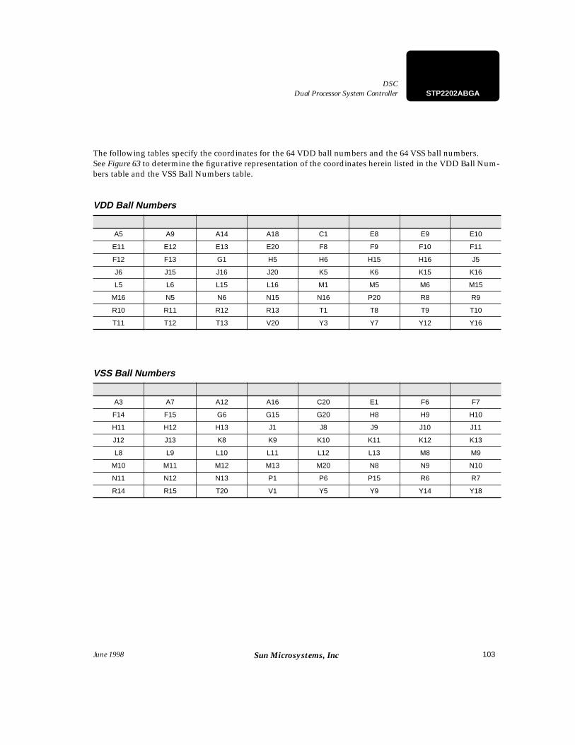
103
Dual Processor System ControllerDSC
STP2202ABGA
June 1998 Sun Microsystems, Inc
The following tables specify the coordinates for the 64 VDD ball numbers and the 64 VSS ball numbers. See Figure 63 to determine the figurative representation of the coordinates herein listed in the VDD Ball Num-bers table and the VSS Ball Numbers table.
VDD Ball Numbers
A5 A9 A14 A18 C1 E8 E9 E10
E11 E12 E13 E20 F8 F9 F10 F11
F12 F13 G1 H5 H6 H15 H16 J5
J6 J15 J16 J20 K5 K6 K15 K16
L5 L6 L15 L16 M1 M5 M6 M15
M16 N5 N6 N15 N16 P20 R8 R9
R10 R11 R12 R13 T1 T8 T9 T10
T11 T12 T13 V20 Y3 Y7 Y12 Y16
VSS Ball Numbers
A3 A7 A12 A16 C20 E1 F6 F7
F14 F15 G6 G15 G20 H8 H9 H10
H11 H12 H13 J1 J8 J9 J10 J11
J12 J13 K8 K9 K10 K11 K12 K13
L8 L9 L10 L11 L12 L13 M8 M9
M10 M11 M12 M13 M20 N8 N9 N10
N11 N12 N13 P1 P6 P15 R6 R7
R14 R15 T20 V1 Y5 Y9 Y14 Y18
104
STP2202ABGA Dual Processor System Controller DSC
June 1998Sun Microsystems, Inc
ORDERING INFORMATION
Part Number Speed Description
STP2202ABGA 100MHz Dual Processor System Controller (DSC)
105
Dual Processor System ControllerDSC
STP2202ABGA
June 1998 Sun Microsystems, Inc
©1998 Sun Microsystems, Inc. All Rights reserved.
THE INFORMATION CONTAINED IN THIS DOCUMENT IS PROVIDED “AS IS” WITHOUT ANY EXPRESS REPRESENTATIONS OF WARRANTIES. INADDITION, SUN MICROSYSTEMS, INC. DISCLAIMS ALL IMPLIED REPRESENTATIONS AND WARRANTIES, INCLUDING ANY WARRANTY OFMERCHANTABILITY, FITNESS FOR A PARTICULAR PURPOSE, OR NON-INFRINGEMENT OF THIRD PARTY INTELLECTURAL PROPERTY RIGHTS.
This document contains proprietary information of Sun Microsystems, Inc. or under license from third parties. No part of this document may be reproducedin any form or by any means or transferred to any third party without the prior written consent of Sun Microsystems, Inc.
Sun, Sun Microsystems,, SPARCstation and the Sun Logo are trademarks or registered trademarks of Sun Microsystems, Inc. in the United States and othercountries. All SPARC trademarks are used under license and are trademarks or registered trademarks of SPARC International, Inc. in the United States andother countries. Products bearing SPARC trademarks are based upon an architecture developed by Sun Microsystems, Inc.
The information contained in this document is not designed or intended for use in on-line control of aircraft, aircraft navigation or aircraft communications;or in the design, construction, operation or maintenance of any nuclear facility. Sun disclaims any express or implied warranty of fitness for such uses.
Part Number: 802-7328-04
Sun Microsystems, Inc.901 San Antonio RoadPalo Alto, CA 94303-4900 USA800/681-8845www.sun.com/microelectronics
STP2202ABGA
Recommended