Embed Size (px)
Citation preview

April 2015 Altera Corporation
TB-111-1.0
© 2015 Altera Corporation. AlNIOS, QUARTUS and STRATTrademark Office and in othetheir respective holders as desproducts to current specificatioproducts and services at any tiof any information, product, oadvised to obtain the latest verfor products or services.
101 Innovation DriveSan Jose, CA 95134www.altera.com
Zynq to SoC FPGA Design Migration Tipsand Techniques
by Todd Koelling, Senior Manager, SoC Product Marketing, Alteraand Joerg Bertholdt, Director of Embedded Software Marketing, Altera
Technical Brief
IntroductionAltera® SoC FPGAs and Xilinx Zynq All Programmable SoCs integrate a dual-core ARM® Cortex®-A9 MPCore™ processor and FPGA logic into a single programmable device. Since their introduction, both families generated significant design activity within the embedded and FPGA development communities. For a number of reasons, including some hardware architectural advantages and the more familiar integrated ARM development flow of Altera SoCs, it is useful to understand and size the task of moving a design from Zynq to Altera SoCs.
No fully automatic tool currently exists to perform this migration. Fortunately, for many users—especially Linux users—the migration process is relatively straight-forward though certainly not trivial. To help designers understand the migration process, this guide provides useful tips garnered from others who successfully converted their designs to SoC FPGAs. Design migration can be an in-house development project or it can be contracted to one of the many highly-experienced design services professionals in Altera’s Design Services Network website.
Design Migration—View from the TopFrom a high level, the similarities between the Xilinx Zynq family and the Altera SoC family are readily apparent, as shown in Figure 1. Both device families integrate a high-performance, 32 bit dual-core ARM Cortex-A9 MPCore processor along with their associated peripherals, all connected to a modern FPGA architecture with integrated hard intellectual property (IP) blocks (RAM blocks, digital signal processing (DSP) blocks, PCI Express® (PCIe®) blocks, high-speed serial transceivers, and so on). In both device families, a hardened DDR memory controller primarily serves the ARM processors and optionally serves functions in the programmable logic (PL) or FPGA. Altera SoCs also provide additional DDR hard memory controllers dedicated to FPGA-based functions. In Zynq, these DDR memory interfaces use PL resources.
l rights reserved. ALTERA, ARRIA, CYCLONE, ENPIRION, HARDCOPY, MAX, MEGACORE, IX words and logos are trademarks of Altera Corporation and registered in the U.S. Patent and r countries. All other words and logos identified as trademarks or service marks are the property of cribed at www.altera.com/common/legal.html. Altera warrants performance of its semiconductor ns in accordance with Altera's standard warranty, but reserves the right to make changes to any
me without notice. Altera assumes no responsibility or liability arising out of the application or use r service described herein except as expressly agreed to in writing by Altera. Altera customers are sion of device specifications before relying on any published information and before placing orders
Feedback Subscribe
ISO 9001:2008 Registered

Page 2 Design Migration—View from the Top
Figure 1. High-Level Comparison of Zynq and Altera SoC Architectures
There are multiple migration steps—some easy, some more difficult—depending on the complexity of the design, the characteristics of the system application, and your familiarity with processor and FPGA development tools. The complete migration process includes the following steps, as shown in Figure 2.
1. Archive the working Zynq application.
2. Acquire the necessary Altera development software.
3. Select the processor boot and FPGA configuration mode that best suits the application: SoC FPGAs support additional modes not available on Zynq.
4. Configure the SoC FPGA processor system and peripherals to best match the Zynq design. (Application software and operating system migration can begin early, while awaiting migration of the FPGA-based logic.)
■ Altera’s Qsys system integration tool simplifies the process of configuring peripherals and system features
■ Leverage new peripheral features, where applicable
■ Configure the bus interfaces between the SoC FPGA’s processor system and the FPGA
■ Configure the interfaces between the FPGA and the processor’s DDR memory controller
■ Connect the various system sideband signals, including DMA requests, interrupt requests, and resets
ARM
Cortex-A9
Hardened DDR Memory Controller Hardened DDR Memory Controller
Processor System (PS) Hard Processor System (HPS)
Xilinx Zynq Altera SoC
ARM
Cortex-A9
ARM
Cortex-A9
ARM
Cortex-A9Processor
Peripherals ProcessorPeripherals
Block RAM
Soft DDR Memory Controller(s)
1 to 3 DDR Hard Memory Controller(s) + ECC
Soft ParallelNOR Flash
DSP
PCI Express
XADC
ParallelNOR Flash
256 KBOn-Chip RAM
64 KBOn-Chip RAM
High-SpeedSerial I/O
Block RAM
DSP
External ADC
PCI Express
High-SpeedSerial I/O
CPU/FPGA
Interface
DDR Memory/FPGA
Interface
CPU/FPGA
Interface
DDR Memory/FPGA
Interface
Programmable Logic (PL) FPGA
April 2015 Altera Corporation Zynq to SoC FPGA Design Migration Tips and Techniques

Design Migration—View from the Top Page 3
5. Migrate the PL design to the FPGA.
■ Usually created using highly-portable VHDL or Verilog
■ Soft- and hard IP block migration requires additional attention
■ Move Zynq PL-side soft DDR memory interfaces to the SoC FPGA’s full-featured hardened memory controllers
6. Automatically generate the hand-off files for operating system support, software development, and FPGA-adaptive software debugging
7. Migrate the operating system
■ Migrating between mutually-supported operating systems is the easiest
■ Migrating bare-metal or custom operating system applications requires more effort
■ Symmetric Multiprocessing (SMP) applications are easier to migrate than Asymmetric Multiprocessing (AMP) applications
8. Migrate the software application
■ Typically written in highly-portable C or C++
■ The ARM Cortex-A9 processor subsystems are nearly identical between Zynq and SoC FPGA
9. Debug the application using the ARM Development Studio 5 (DS-5™) Altera Edition Toolkit, which provides enhanced, FPGA-adaptive debugging capabilities
April 2015 Altera CorporationZynq to SoC FPGA Design Migration Tips and Techniques

Page 4 Before You Begin
Figure 2. The Complete Migration Process
Before You Begin
Archive Now!Before you begin the migration process, be sure to archive the entire working Zynq application, including code for both the processing system (PS) and PL portions. The archive is inexpensive insurance against accidental design changes that might creep in during the migration process.
The Right Tool for the JobAs with Zynq development, Altera’s development software targets both software and hardware design, as shown in Table 1. Altera’s SoC Embedded Design Suite (SoC EDS) primarily targets the ARM Cortex-A9 and the SoC FPGA’s hard processor system (HPS). The SoC EDS also includes the ARM DS 5Altera Edition software, including advanced FPGA-adaptive debugging.
Archive the working SoC application
Migrate the programmable logic design
Migrate the operating system
Generate hand-off files
Optionally begin softwaredevelopment on Hard Processor
System (HPS), withoutFPGA-based functionality
Migrate the application software
Debug, validate the SoC application
Acquire the necessary Alteradevelopment software
Choose the boot and configurationmode best for the application
Configure the processor systemand peripherals, including
FPGA-based peripherals
AlteraSoC
XilinxZynqSoC
April 2015 Altera Corporation Zynq to SoC FPGA Design Migration Tips and Techniques
Before You Begin Page 5
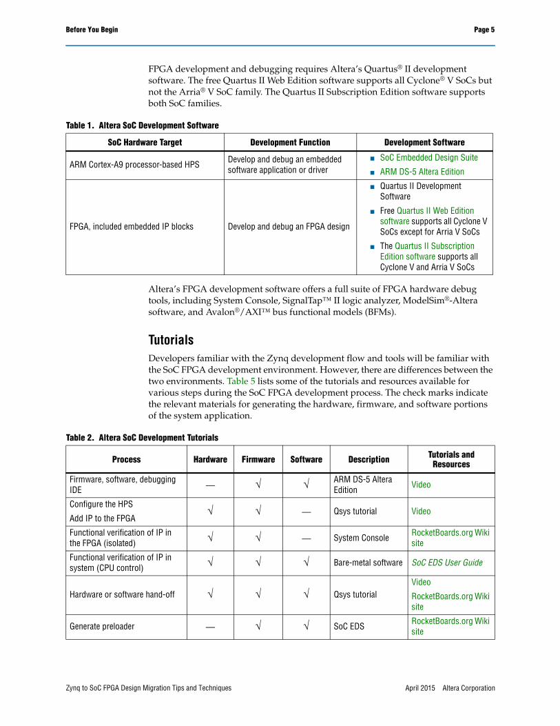
FPGA development and debugging requires Altera’s Quartus® II development software. The free Quartus II Web Edition software supports all Cyclone® V SoCs but not the Arria® V SoC family. The Quartus II Subscription Edition software supports both SoC families.
Altera’s FPGA development software offers a full suite of FPGA hardware debug tools, including System Console, SignalTap™ II logic analyzer, ModelSim®-Altera software, and Avalon®/AXI™ bus functional models (BFMs).
TutorialsDevelopers familiar with the Zynq development flow and tools will be familiar with the SoC FPGA development environment. However, there are differences between the two environments. Table 5 lists some of the tutorials and resources available for various steps during the SoC FPGA development process. The check marks indicate the relevant materials for generating the hardware, firmware, and software portions of the system application.
Table 1. Altera SoC Development Software
SoC Hardware Target Development Function Development Software
ARM Cortex-A9 processor-based HPS Develop and debug an embedded software application or driver
■ SoC Embedded Design Suite
■ ARM DS-5 Altera Edition
FPGA, included embedded IP blocks Develop and debug an FPGA design
■ Quartus II Development Software
■ Free Quartus II Web Edition software supports all Cyclone V SoCs except for Arria V SoCs
■ The Quartus II Subscription Edition software supports all Cyclone V and Arria V SoCs
Table 2. Altera SoC Development Tutorials
Process Hardware Firmware Software Description Tutorials and Resources
Firmware, software, debugging IDE — √ √ ARM DS-5 Altera
Edition Video
Configure the HPS
Add IP to the FPGA √ √ — Qsys tutorial Video
Functional verification of IP in the FPGA (isolated) √ √ — System Console RocketBoards.org Wiki
site
Functional verification of IP in system (CPU control) √ √ √ Bare-metal software SoC EDS User Guide
Hardware or software hand-off √ √ √ Qsys tutorialVideo
RocketBoards.org Wiki site
Generate preloader — √ √ SoC EDS RocketBoards.org Wiki site
April 2015 Altera CorporationZynq to SoC FPGA Design Migration Tips and Techniques

Page 6 Choose a Boot and Configuration Mode Best for Your Application
Choose a Boot and Configuration Mode Best for Your ApplicationWhy choose a boot and configuration mode as the first step in the migration process? Zynq devices support one boot and configuration mode: the processor always boots first and then the processor loads the PL (FPGA) portion of the device. SoC FPGAs support the same mode but also offer two additional modes, as shown in Figure 5. In SoC FPGAs, the FPGA can configure first, connecting the CPU to boot devices or communication paths via the FPGA logic. Alternatively, both the CPU can boot and the FPGA can configure independently.
Figure 3. Zynq and Altera SoC Boot and Configuration Modes
Choosing a boot and configuration mode has direct implications on the next step—configuring the processor peripherals.
Configuring the Processor System and PeripheralsWhile the ARM Cortex-A9 processing subsystems in the Zynq and SoC FPGA families are nearly identical, there are differences in the dedicated peripheral set, as shown in Figure 4. Fortunately, mapping from Zynq peripherals to SoC FPGA peripherals is relatively straightforward. There may be differences if a different boot or configuration mode is selected plus some differences in peripheral offerings or features. See the warning signs in Figure 4.
Debug software connected to target board — √ √ User space
application SoC EDS User Guide
Debug software connected to target board — √ √ Kernel driver SoC EDS User Guide
Linux kernel debugging — √ √ ARM DS-5 Altera Edition Video
Bare-metal debugging and trace √ √ √ ARM DS-5 Altera Edition Video
FPGA-adaptive debugging √ √ √ ARM DS-5 Altera Edition Video
Program flash memory (Hardware image and software image)
√ √ √ HPS flash programmer SoC EDS User Guide
Hardware or software cross triggering (advanced topic) √ √ √
Triggering between SignalTap II logic analyzer and debugger
SoC EDS User Guide
Table 2. Altera SoC Development Tutorials
Process Hardware Firmware Software Description Tutorials and Resources
CPU Boots, Configures FPGA
Xilinx Zynq Altera SoC
CPU Boots, Configures FPGA
Configure FPGA, CPU Boots thru FPGA
Independent FPGA Configuration, CPU Boot
April 2015 Altera Corporation Zynq to SoC FPGA Design Migration Tips and Techniques

Configuring the Processor System and Peripherals Page 7
Figure 4. Zynq to Altera SoC Processor and Peripheral Migration
The Altera Qsys system integration tool greatly simplifies the setting up of the processor system and peripherals on SoC FPGAs, as shown in the SoC HPS System Generation Using Qsys training video on the YouTube website.
While the processor peripheral sets are roughly equivalent, there are a few significant differences. Zynq and SoC FPGA provide similar but architecturally different interfaces between the processor system and programmable logic, and between the programmable logic and the processor’s DDR memory controller.
f For more information, refer to the “Interface Differences between Zync and SoC FPGA” on page 8.
Zynq software applications are constrained to a 1 gigabyte (GB) address space while SoC FPGAs support the full 4 GB address space allowed with a 32 bit address. While Zynq’s DDR memory controller supports error correction code (ECC) functions only for a 16 bit memory interface, SoC FPGAs add ECC support for 32 bit wide memory interfaces.
GPIO
Application Code
256 KB On-chip RAM
2x 12C
2x SPI Controller
Interfaces to FPGA-basedPeripherals
IP Library Functions
Parallel NOR Flash
Security (AES, SHA, RSA)
XADC
24 bit Watchdog Timer
2x 16 bit Triple-Mode Counters
2x CAN
2x UART
SD/SDIO Controller
2x USB On-The-Go (OTG)
2x 10/100/1G Ethernet
NAND Controller, SLC
Quad SPI Controller
8-Channel DMA Controller
(x16, x16+ECC, x32)(DDR2, DDR3, LPDDR2)
Hard DDR Memory Controller
Programmable Logic
Xilinx Zynq
Interfaces to FPGA-based Peripherals
GPIO
IP Library Functions
Security (AES, ECSDA, public key)
Security (AES)
External A/D Device (s)
2x 32 bit Watchdog Timers
4x 32 bit General-Purpose Counters
2x SPI Master Controllers
2x CAN
4x I2C
2x UART
SD/MMC/SDIO Controller
2x USB On-The-Go (OTG)
2x 10/100/1G Ethernet
NAND Controller, SLC or MLC
Quad SPI Controller
256 KB On-Chip RAM
64 KB On-Chip RAM
8-channel DMA Controller
FPGA Fabric
Application Code
Hard DDR Memory Controller (CPU)
2x SPI Slave Controllers
Altera SoC
Convert to Quad SPI
Parallel NOR Flash in FPGA
(x8, x16, x16+ECC, x32, x32+ECC)(DDR2, DDR3, LPDDR2)
as part of FPGA design
C/C++VHDL/Verilog/OpenCL™
Cyclone V, Arria V
Arria 10
= Warning
Cyclone V, Arria V
Arria 10
April 2015 Altera CorporationZynq to SoC FPGA Design Migration Tips and Techniques
Page 8 Configuring the Processor System and Peripherals
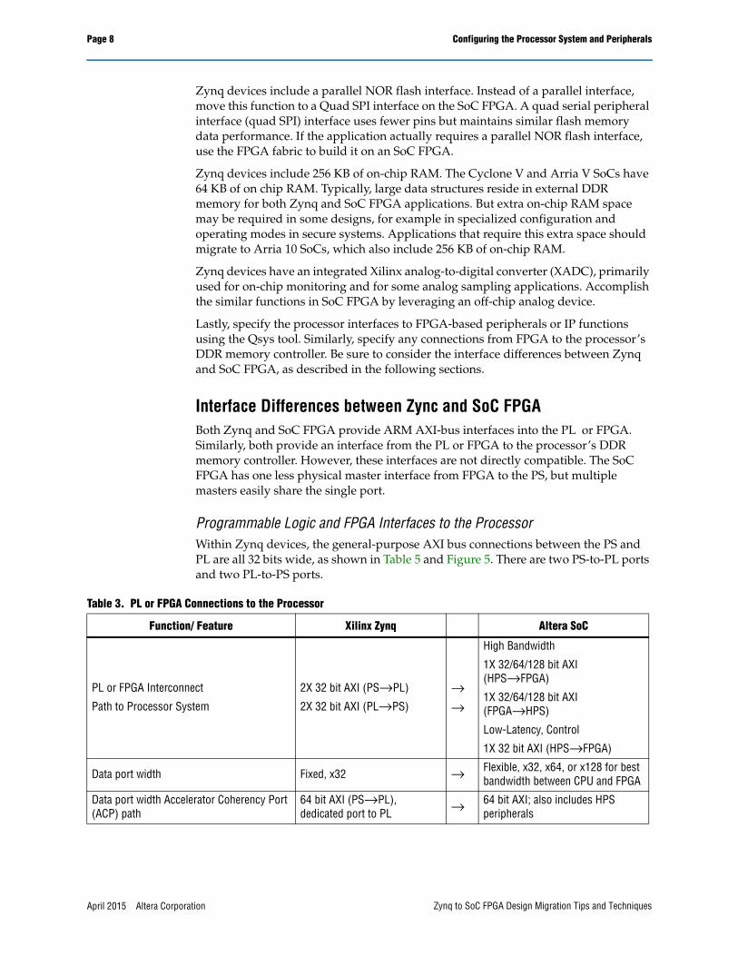
Zynq devices include a parallel NOR flash interface. Instead of a parallel interface, move this function to a Quad SPI interface on the SoC FPGA. A quad serial peripheral interface (quad SPI) interface uses fewer pins but maintains similar flash memory data performance. If the application actually requires a parallel NOR flash interface, use the FPGA fabric to build it on an SoC FPGA.
Zynq devices include 256 KB of on-chip RAM. The Cyclone V and Arria V SoCs have 64 KB of on chip RAM. Typically, large data structures reside in external DDR memory for both Zynq and SoC FPGA applications. But extra on-chip RAM space may be required in some designs, for example in specialized configuration and operating modes in secure systems. Applications that require this extra space should migrate to Arria 10 SoCs, which also include 256 KB of on-chip RAM.
Zynq devices have an integrated Xilinx analog-to-digital converter (XADC), primarily used for on-chip monitoring and for some analog sampling applications. Accomplish the similar functions in SoC FPGA by leveraging an off-chip analog device.
Lastly, specify the processor interfaces to FPGA-based peripherals or IP functions using the Qsys tool. Similarly, specify any connections from FPGA to the processor’s DDR memory controller. Be sure to consider the interface differences between Zynq and SoC FPGA, as described in the following sections.
Interface Differences between Zync and SoC FPGABoth Zynq and SoC FPGA provide ARM AXI-bus interfaces into the PL or FPGA. Similarly, both provide an interface from the PL or FPGA to the processor’s DDR memory controller. However, these interfaces are not directly compatible. The SoC FPGA has one less physical master interface from FPGA to the PS, but multiple masters easily share the single port.
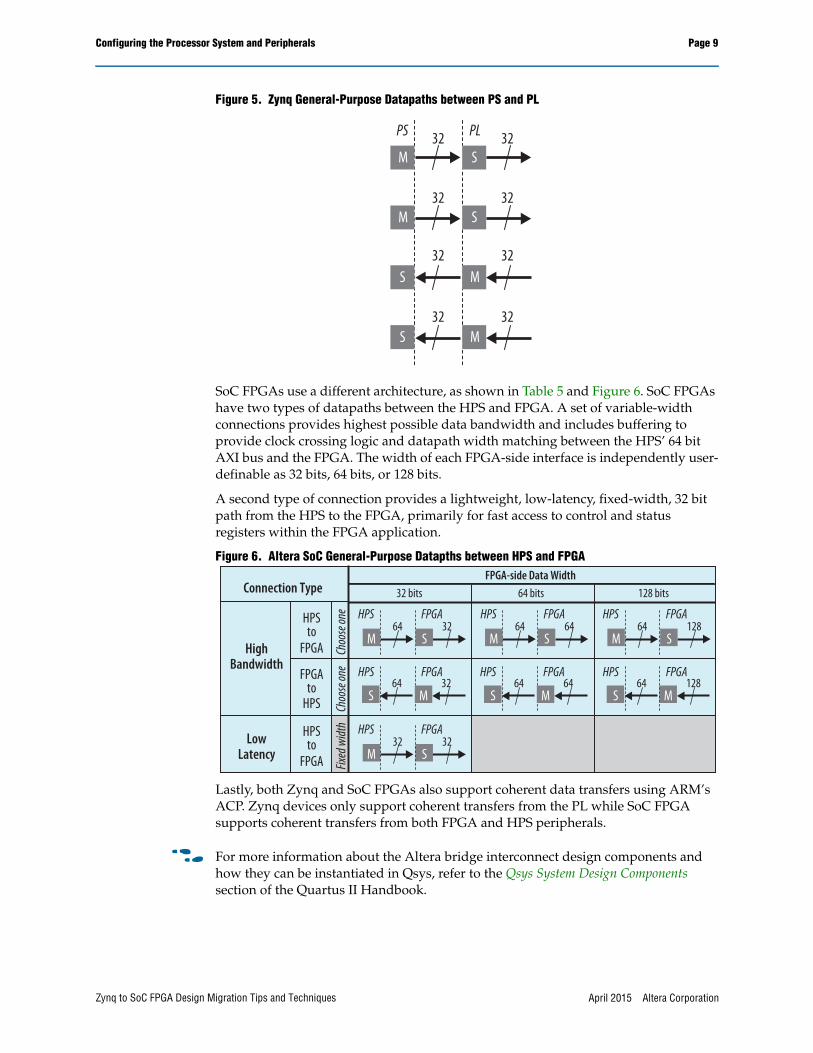
Programmable Logic and FPGA Interfaces to the ProcessorWithin Zynq devices, the general-purpose AXI bus connections between the PS and PL are all 32 bits wide, as shown in Table 5 and Figure 5. There are two PS-to-PL ports and two PL-to-PS ports.
Table 3. PL or FPGA Connections to the Processor
Function/ Feature Xilinx Zynq Altera SoC
PL or FPGA Interconnect
Path to Processor System
2X 32 bit AXI (PS→PL)
2X 32 bit AXI (PL→PS)
→→
High Bandwidth
1X 32/64/128 bit AXI (HPS→FPGA)
1X 32/64/128 bit AXI (FPGA→HPS)
Low-Latency, Control
1X 32 bit AXI (HPS→FPGA)
Data port width Fixed, x32 → Flexible, x32, x64, or x128 for best bandwidth between CPU and FPGA
Data port width Accelerator Coherency Port (ACP) path
64 bit AXI (PS→PL), dedicated port to PL → 64 bit AXI; also includes HPS
peripherals
April 2015 Altera Corporation Zynq to SoC FPGA Design Migration Tips and Techniques
Configuring the Processor System and Peripherals Page 9
Figure 5. Zynq General-Purpose Datapaths between PS and PL
SoC FPGAs use a different architecture, as shown in Table 5 and Figure 6. SoC FPGAs have two types of datapaths between the HPS and FPGA. A set of variable-width connections provides highest possible data bandwidth and includes buffering to provide clock crossing logic and datapath width matching between the HPS’ 64 bit AXI bus and the FPGA. The width of each FPGA-side interface is independently user-definable as 32 bits, 64 bits, or 128 bits.
A second type of connection provides a lightweight, low-latency, fixed-width, 32 bit path from the HPS to the FPGA, primarily for fast access to control and status registers within the FPGA application.
Figure 6. Altera SoC General-Purpose Datapths between HPS and FPGA
Lastly, both Zynq and SoC FPGAs also support coherent data transfers using ARM’s ACP. Zynq devices only support coherent transfers from the PL while SoC FPGA supports coherent transfers from both FPGA and HPS peripherals.
f For more information about the Altera bridge interconnect design components and how they can be instantiated in Qsys, refer to the Qsys System Design Components section of the Quartus II Handbook.
32 32
32 32
32 32
32 32
PS PL
M
S
S
S
M
M
M S
32 bits 64 bits 128 bits
FPGA-side Data WidthConnection Type
HighBandwidth
LowLatency
HPSto
FPGA
HPSto
FPGA
FPGAto
HPS
Fixed
widt
h
HPS FPGA
HPS FPGA
HPS FPGA
Choo
se on
eCh
oose
one HPS FPGA HPS FPGA
HPS FPGA HPS FPGA
64 32
32 32
64 32
64 64 64 128
64 64 64 128
M S
M S
S M
M S M S
S M S M
April 2015 Altera CorporationZynq to SoC FPGA Design Migration Tips and Techniques

Page 10 Migrating PL to FPGA
PL and FPGA Interfaces to the Processor’s DDR Memory ControllerBoth Zynq and SoC FPGA include a high-performance datapath between the PL or FPGA and the processor’s DDR memory controller, as listed in Table 4. Zynq has four 64 bit AXI-bus connections from the PL, multiplexed down to just two ports in the Zynq memory interconnect switch.
SoC FPGA has a direct 256 bit connection to the processor’s DDR memory that the FPGA application can allocate among different bus standards (AXI or Avalon Memory Mapped (Avalon-MM) interface) and different port widths (32, 64, 128, or 256 bits). The interface supports up to six command or response ports.
Additionally, the SoC FPGA interface includes a memory protection unit—similar to the processor’s MPU—that prevents accidental data corruption from FPGA-side data transactions.
System Sideband Signals (DMA Requests, Interrupts, and Resets)Besides the data bus connections, there are also various asynchronous control connections to the PL or FPGA. These controls include clocks, DMA requests, interrupt requests, and resets to and from the PL or FPGA.
In Zynq, a Watchdog Timer reset event always causes the entire system to reconfigure. In SoC FPGA, the response to a Watchdog Timer reset event is defined by the application. SoC FPGAs can reconfigure the FPGA fabric, similar to Zynq, or just reset specific flip-flops or functions within the FPGA application without reconfiguring the FPGA.
Migrating PL to FPGABoth the Zynq and SoC FPGAs integrate leading-edge PL or FPGA fabric, as shown in Figure 1. Migrating a between the two is generally straightforward but requires some translation effort, as shown in Figure 7.
Table 4. PL or FPGA Connections to Processor’s DDR Memory Controller
Function/ Feature Xilinx Zynq Altera SoC
PL or FPGA interconnect path to DDR memory controller 4X 64 bit AXI → 256 bit AXI or Avalon-MM with
configurable port width
Maximum interconnect ports4X 64 bit read ports
4X 64 bit write ports→
6 command or response ports
4 read ports
4 write ports
Port-size options 32/64 bits → 32/64/128/256 bits
Memory protection unit N/A → Yes
April 2015 Altera Corporation Zynq to SoC FPGA Design Migration Tips and Techniques

Migrating PL to FPGA Page 11
Figure 7. Migrating PL to FPGA in an Altera SoC
The Zynq PL also includes a variety of specialty hardened IP blocks, such as clock management blocks, block RAM, DSP blocks, PCIe interfaces, and so on. These functions are typically instantiated from within the HDL source files. Altera SoC integrates similar—but not identical—hard IP features so some translation may be required. An SoC FPGA IP block can be substituted, either directly in the source file or by creating an extra layer of VHDL or Verilog hierarchy to insulate and abstract away the hardware differences.
The speed of serial transceivers varies between the two families, so in some cases the transition from lower-speed to higher-speed transceivers may require some design attention.
The Zynq design may also include soft IP cores either from Xilinx or third parties. Similar IP cores may be available from Altera or its partners (For a complete listing, refer to the Intellectual Property page on the Altera website). As with the hard IP blocks, some translation effort is required, either directly or by adding a layer of abstraction.
Zynq devices have only one hard DDR memory controller, as part of the PS. One or more additional soft DDR memory controllers may be built from PL, separate from the processor’s hard memory controller. When migrating to an SoC FPGA, however, these soft memory controllers can by replaced by the one to three sophisticated hard memory controllers integrated within the FPGA fabric (see Figure 1), and compatible with the processor’s memory controller. Additional memory controllers can also be built using soft IP.
Serial Transceivers
DMA Requests from PL
Resets to/from PL
Interrupts to/from PL
Resets to/from FPGA
Interrupts to/from FPGA
32/64 bit Interface to PS DDR Controller
32 bit PS/PL AXI Interface 32/64/128 bit CPU/FPGA Interface
Low-latency 32 bit CPU/FPGA Interface32/64/128/256 bit Interface to HPS
Soft DDR Memory Interface(s)
Soft IP Cores Soft IP Cores
PCI Express Blocks
32 Kb Block RAM
DSP Blocks
Programmable Logic
MMCMs
Xilinx Zynq
DMA Requests from FPGA
DDR Controller
Hard DDR Memory Controller(s)
Soft DDR Memory Interface(s)
Hi-Speed Serial Transceivers
FPGA Fabric
PCI Express Blocks
Phase-Locked Loops (PLLs)M10K Block RAM
Variable-Precision DSP Blocks
Variable-Precision DSP Blocks with
Altera SoC VHDL/Verilog/OpenCL
Cyclone V, Arria V
Arria 10
Hardened Floating-Point Support
April 2015 Altera CorporationZynq to SoC FPGA Design Migration Tips and Techniques

Page 12 Generating the Hand-Off Files
Generating the Hand-Off FilesAfter configuring the SoC FPGA system, automatically generate hand-off files specifically customized to the hardware specification. As shown in Figure 8, these files provide register definitions for software development and debugging plus used by the Device Tree builder for operating system support.
Figure 8. Generate Hand-Off Files for Software Development and Operating System Support
The Operating System Abstracts Processor PeripheralsGenerally, most of the application software is highly portable between Zynq and SoC FPGA. After all, the software application is migrating from one ARM Cortex-A9 variant to another. The portability of the peripheral interfaces, however, depends on the operating system—or the lack of an operating system in a bare-metal application. Essentially, the operating system provides an abstraction layer between the software application running on the processor and the processor’s peripherals. The operating system creates a more uniform software application interface across different hardware.
System Built Using a Mutually-Supported Operating SystemIf using an operating system, simply configure the dedicated processor peripherals in the HPS using Altera’s Qsys SoC development software. Then, recompile your software application with the software-generated device tree or vendor-supplied board support package. The operating system and its support files insulate the application software against most low-level changes to address register locations, interrupt vectors, and so on.
Device DriverDefinitions
Register Definitions
Generate
Hand-off Files
Device Tree
Builder
ARM DS-5
Altera Edition
Linux, VxWorksor other OS with
Device TreeSupport
Hard Processor
System (HPS)
FPGA
April 2015 Altera Corporation Zynq to SoC FPGA Design Migration Tips and Techniques

The Operating System Abstracts Processor Peripherals Page 13
Figure 9. Linux Operating System Options
LinuxLinux is the most popular operating system choice for Zynq and SoC FPGAs, as it is for most application-class embedded processing applications. When this document was created, there were five different variants of Linux available for Zynq devices, shown in Figure 9, including one version supported by the Yotco build environment and a commercial version of Linux from Wind River.
Altera supports a variety of open-source and commercial versions of Linux as well, including the popular Ångström Distribution. To provide a more stable and compatible version for consumer electronics, Altera supports versions of Linux under the Long Term Support Initiative (LTSI). Similarly, Altera supports one version under the Yotco build environment and a commercial version of Linux from Wind River.
To migrate an application:
■ Configure the SoC FPGA peripherals using the Altera Qsys tool
■ Generate the associated hand-off files for the Device Tree Builder
■ Recompile the operating system and application
Linux Design and Development SupportThe RocketBoards website (www.RocketBoards.org) provides links and resources for Linux developers using SoC FPGAs. The site includes the following:
■ Latest information on Linux support for SoC FPGAs
■ Links to SoC FPGA development boards
■ Linux code repositories
■ Build recipes
■ Developer community and support mailing list
Other Commercial, Mutually-Supported Operating SystemsBesides Linux, other operating systems support both the Zynq and SoC FPGA platforms. Figure 10 provides a sample of the popular offerings available today, with more added all the time. A complete list of operating systems supported on SoC FPGA is available on the Altera SoC Ecosystem page on the Altera website.
Yocto
Wind River Linux
Ubuntu
Xilinx OSL
PetaLinux
Xilinx Zynq
LTSI Linux
www.RocketBoards.org
Angstrom DistributionYocto Project-powered Embedded Linux
Wind River LinuxConfigure peripheralsGenerate support filesRecompile application
Altera SoC
April 2015 Altera CorporationZynq to SoC FPGA Design Migration Tips and Techniques

Page 14 The Operating System Abstracts Processor Peripherals
Figure 10. More Popular, Mutually-Supported Commercial Operating Systems
If the operating system uses a device tree to integrate the necessary drivers (for example, Wind River VxWorks), then create a custom device tree using the automatically generated hand-off files and the device tree generator. If the operating system does not use a device tree, then manually integrate the drivers within the operating system’s specific driver infrastructure.
Bare-Metal SystemsMigrating bare-metal applications requires considerably more development effort than if exploiting a supported operating system. Without an operating system, the software application must directly control the peripheral hardware, thereby requiring intimate knowledge of register locations, interrupt vectors, and hardware functionality.
To accelerate bare-metal and proprietary operating system development, Altera provides a hardware library (HWLIB) that supports low-level access to the SoC FPGA features, shown in Figure 11. The hardware library includes an application programming interface (API) to an SoC Abstraction Layer (SoCAL), which provides a logical abstraction to physical peripherals, registers, and even bit-fields within registers. Additionally, HWLIB includes a Hardware Manager (HW Manager) API for pre-defined, device-specific configuration and control functions.
ENEA OSE
iVeia Android Fujisoft Android
Micrium uC/OS
Green Hills INTEGRITY
Adeneo QNX
Wind River VxWorks
Express Logic ThreadX
Xilinx Zynq
ENEA OSE
Wind River VxWorks
Micrium uC/OS-II, uC/OS-III
Express Logic ThreadX
Green Hills INTEGRITY
QNX Neutrino RTOS
Altera SoC
Configure peripheralsCreate support filesRecompile application
April 2015 Altera Corporation Zynq to SoC FPGA Design Migration Tips and Techniques

The Easy Part—Migrating the Application Software Page 15
Figure 11. HW Manager Provides Abstraction of Low-Level Functions
SMP Simplifies the Migration Process, but AMP is a Major ProjectThe dual-core ARM Cortex-A9 processor enables new processing techniques not available for single-core systems. SMP, where both processors operate independently but under a common operating system, is the most common multiprocessor programming model. Modern versions of Linux and VxWorks support SMP, use of which simplifies the migration process from Zynq to SoC FPGA.
In asymmetric multiprocessing (AMP), each processor operates independently, each running its own distinct operating system. For example, one processor may run a full-featured operating system while the other runs a smaller real-time operating system (RTOS).
Creating and migrating AMP designs can be painful, primarily because the two independent operating systems share the Level 2 (L2) cache, peripherals, and other hardware. Often, AMP implementations result in longer latency when accessing shared peripherals due to arbitration and less coherency. Additionally, there are subtle differences in L2 cache connectivity between Zynq and Altera SoC. These issues are not showstoppers, but certainly complicate the migration process for AMP designs.
If possible, consider migrating an AMP-style implementation over to an SMP-style implementation for better performance, support, and maintainability.
The Easy Part—Migrating the Application SoftwareThe application software is perhaps the easiest portion of the design to migrate. In most designs, the application software is written in C or C++. Additionally, the underlying ARM Cortex-A9 processor subsystem is nearly identical between Zynq and SoC FPGA. One of the advantages of recompiling in the ARM DS-5 environment is that the ARM Compiler 5 included with the DS-5 software automatically vectorizes C or C++ code for the Cortex-A9’s NEON™ media coprocessor or floating-point unit, potentially saving a lot of manual code optimization.
With Operating System
HW LibrarySoC Abstraction Layer
(SoCAL)
User Application Software
SoC FPGA Hardware(Registers, interrupts, etc.)
SoC FPGA Hardware(Registers, interrupts, etc.)
Bare-Metal Application
Bare-Metal Application
Full-featured Operating System
Abstra
ctio
nBSP/OS Driver Model
HW LibraryHardwareLibrary
SoC Abstraction Layer(SoCAL)
April 2015 Altera CorporationZynq to SoC FPGA Design Migration Tips and Techniques

Page 16 Debugging and Verification Support
Debugging and Verification SupportThe ARM DS-5 Altera Edition Toolkit provides significant advantages for faster application development, board bring-up, and operating system development. Additionally, FPGA-adaptive debugging brings both the processor and FPGA-based functions into view.
■ Whole-chip, FPGA-adaptive debugging, encompassing both processors and FPGA-based functions
■ Register visibility across the entire design
■ Cross-triggering and in-system trace
■ Monitoring software, CPU, and FPGA hardware events
■ ARM System Trace Macrocell (STM) for timestamping events in trace data stream, even from FPGA-based bus masters
■ True multicore debugging
■ Performance profiling of CPU and FPGA processes
■ Native Linux support for hardware-assisted trace
f For a deeper understanding, refer to the System Trace Macrocell Packs Major Benefits for High-Performance SoC System Debug White Paper.
SoC FPGA’s Common Footprint Provides Extra Design FlexibilityAt the board level, packages and pin-outs may also differ between the two families. Designs using the Cyclone V SoC packages shown in Figure 12 can migrate between devices of different gate densities and between devices with or without transceivers. Note that the 672-ball package offers complete density migration between devices of different gate capacities, plus the added flexibility to migrate between devices with and without high-speed serial transceivers. Thus a single printed-circuit board design can support different potential product variants, each using the cost-optimized SoC FPGA that best meets the demands of the application.
Figure 12. Density and Feature Migration between Cyclone V SoC Packages
Package Balls
Package Option484
I/OType
FPGAUserI/Os
DeviceFamily
Cyclone V SoC(without
transceivers)
Cyclone V SoC
Hard Processor System I/O(HPS, including DDR memory
dedicated I/O)
(withouttransceivers)
LogicCapacity
(KLEs)
672 89631x3123x2319x19
0.825
40
40
85
85
110
110
25
181181151
0.8 1.0Package (mm)
Ball Pitch (mm)
I/O Count(Transceiver
Pairs)
66
66
66
66
138
138
138
138
138 (6)
138 (6)
138 (6)
138 (6)
288
288
288 (9)
288 (9)
April 2015 Altera Corporation Zynq to SoC FPGA Design Migration Tips and Techniques

Conclusion Page 17
The Arria V SoC family provides similar package migration flexibility, as shown in Figure 13. All Arria V SoC variants have high-speed serial transceivers.
Figure 13. Density and Feature Migration between Arria V SoC Packages
ConclusionWhile no automated migration tools exist, to migrate an existing Zynq design to an Altera SoC manually can be a straightforward process, depending on the complexity and characteristics of the design. Many pieces of the design will migrate with little attention, while others may require adjustment or use of wrappers to adapt to detailed differences between the two families.
Is the migration task worth it? Many applications directly benefit from Altera SoC’s hardware and software differences, as more thoroughly described in the Architecture Matters: Choosing the Right SoC FPGA for Your Application White Paper. Nor should a design team underestimate the advantages of system development exploiting ARM’s DS-5 Altera Edition software. Further production cost savings, greater package flexibility, and higher system performance also figure in. This guide gives you a basis for understanding and sizing the migration task to reach an appropriate decision.
Further InformationTo learn more, refer to the following resources:
■ Altera SoC Overviewwww.altera.com/products/soc/overview.html
■ Altera SoC Developer Resourceswww.altera.com/products/soc/overview/SoCResourceGuide/Introduction.html
■ Altera Forum: SoCwww.alteraforum.com/forum/forumdisplay.php?f=76
■ Operating System (OS) Support for Altera SoCswww.altera.com/products/soc/portfolio/cyclone-v-soc/ecosystem.html
■ Software Download Centerwww.altera.com/downloads/download-center.html
■ Software Licensingwww.altera.com/download/licensing/lic-index.html
Package Balls
Package Option896
I/OType
FPGAUserI/Os
DeviceFamily
Arria V SoC(without
transceivers)
Hard Processor System I/O(HPS, including DDR memory
dedicated I/O)
LogicCapacity
(KLEs)
1152 151740x4035x3531x31
1.0
350
460
208208208
1.0 1.0Package (mm)
Ball Pitch (mm)
I/O Count(Transceiver
Pairs)
250 (12) 385 (18) 540 (30)
250 (12) 385 (18) 540 (30)
April 2015 Altera CorporationZynq to SoC FPGA Design Migration Tips and Techniques

Page 18 Document Revision History
Document Revision HistoryTable 5 lists the revision history for this document.
Table 5. Document Revision History
Date Version Changes
April 2015 1.0 Initial release.
April 2015 Altera Corporation Zynq to SoC FPGA Design Migration Tips and Techniques