Embed Size (px)
Citation preview
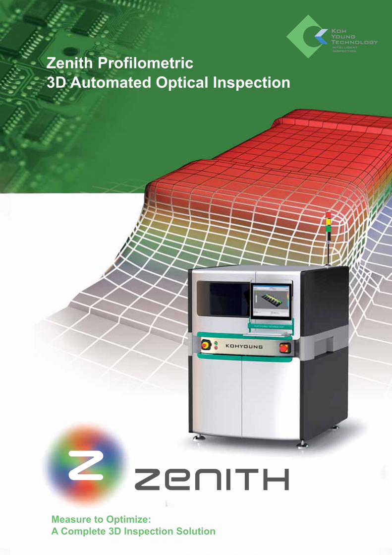
Zenith Profilometric3D Automated Optical Inspection
Measure to Optimize: A Complete 3D Inspection Solution
Zenith 3D AOI with RevolutionaryNew 3D Measurement
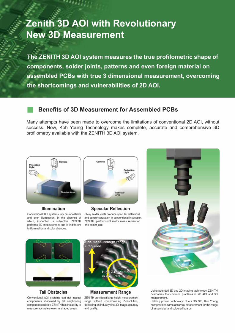
Wide measurement range is required.
High Z-resolutionis required
The ZENITH 3D AOI system measures the true profilometric shape of components, solder joints, patterns and even foreign material on assembled PCBs with true 3 dimensional measurement, overcomingthe shortcomings and vulnerabilities of 2D AOI.
Benefits of 3D Measurement for Assembled PCBs
Many attempts have been made to overcome the limitations of conventional 2D AOI, without success. Now, Koh Young Technology makes complete, accurate and comprehensive 3D profilometry available with the ZENITH 3D AOI system.
Using patented 3D and 2D imaging technology, ZENITH overcomes the common problems in 2D AOI and 3D measurement.Utilizing proven technology of our 3D SPI, Koh Young now provides same accuracy measurement for the range of assembled and soldered boards.
Conventional AOI systems rely on repeatable and even illumination. In the absence of which, inspection is subjective. ZENITH performs 3D measurement and is indifferent to illumination and color changes.
Illumination
and sensor saturation in conventional inspection.ZENITH performs volumetric measurement of the solder joint.
Specular Reflection
Conventional AOI systems can not inspect components shadowed by tall neighboring components reliably. ZENITH has the ability to measure accurately even in shaded areas.
Tall ObstaclesZENITH provides a large height measurement range without compromising Z-resolution, delivering an industry first 3D image accuracy and quality.
Measurement Range
Shiny solder joints produce specular reflections
Measured lead height valueexceeds tolerance
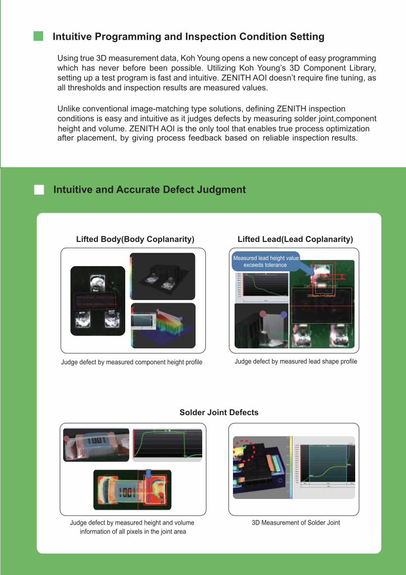
Using true 3D measurement data, Koh Young opens a new concept of easy programming which has never before been possible. Utilizing Koh Young’s 3D Component Library, setting up a test program is fast and intuitive. ZENITH AOI doesn’t require fine tuning, as all thresholds and inspection results are measured values.
Unlike conventional image-matching type solutions, defining ZENITH inspectionconditions is easy and intuitive as it judges defects by measuring solder joint,componentheight and volume. ZENITH AOI is the only tool that enables true process optimization after placement, by giving process feedback based on reliable inspection results.
Intuitive Programming and Inspection Condition Setting
Lifted Body(Body Coplanarity)
Solder Joint Defects
Lifted Lead(Lead Coplanarity)
Judge defect by measured component height profile
Judge defect by measured height and volumeinformation of all pixels in the joint area
Judge defect by measured lead shape profile
3D Measurement of Solder Joint
Intuitive and Accurate Defect Judgment
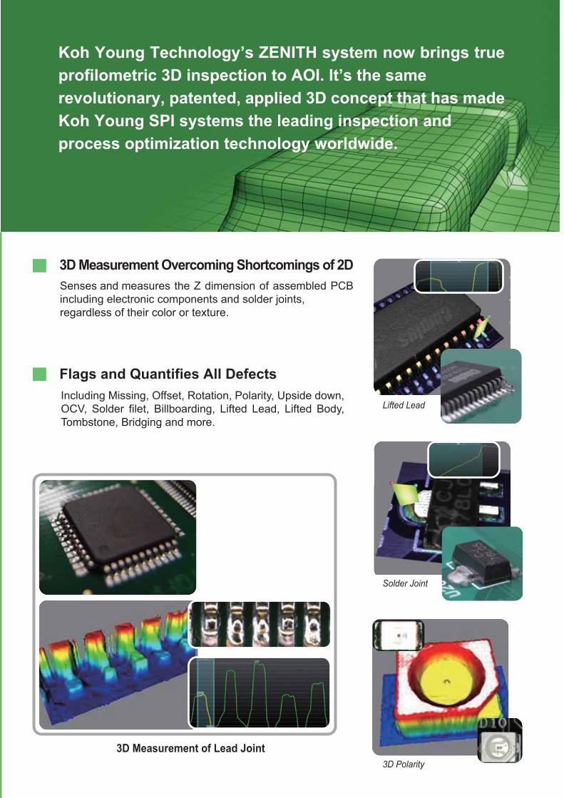
3D Measurement of Lead Joint
Senses and measures the Z dimension of assembled PCB including electronic components and solder joints,regardless of their color or texture.
Including Missing, Offset, Rotation, Polarity, Upside down, OCV, Solder filet, Billboarding, Lifted Lead, Lifted Body, Tombstone, Bridging and more.
Koh Young Technology’s ZENITH system now brings true profilometric 3D inspection to AOI. It’s the samerevolutionary, patented, applied 3D concept that has made Koh Young SPI systems the leading inspection andprocess optimization technology worldwide.
3D Measurement Overcoming Shortcomings of 2D
Flags and Quantifies All Defects
Lifted Lead
Solder Joint
3D Polarity
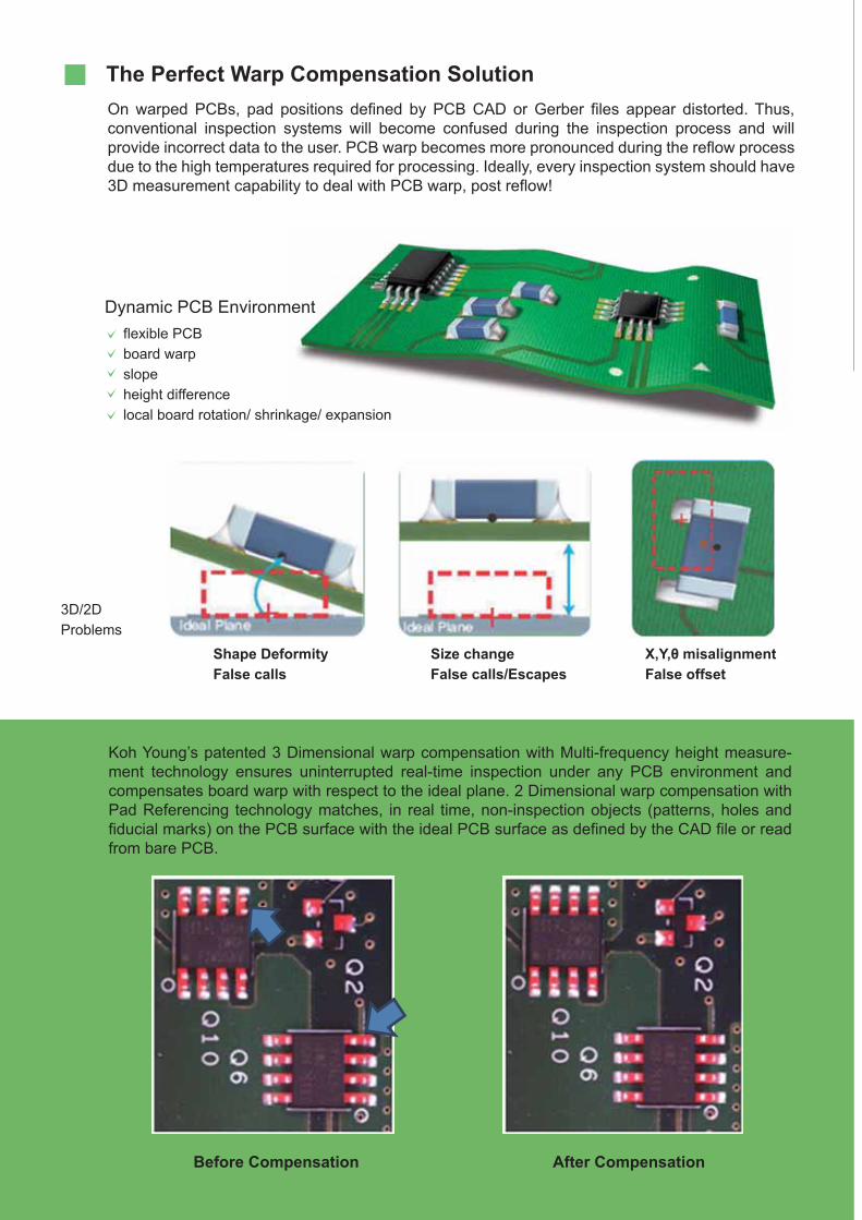
The Perfect Warp Compensation SolutionOn warped PCBs, pad positions defined by PCB CAD or Gerber files appear distorted. Thus, conventional inspection systems will become confused during the inspection process and will provide incorrect data to the user. PCB warp becomes more pronounced during the reflow process due to the high temperatures required for processing. Ideally, every inspection system should have 3D measurement capability to deal with PCB warp, post reflow!
Koh Young’s patented 3 Dimensional warp compensation with Multi-frequency height measure-ment technology ensures uninterrupted real-time inspection under any PCB environment and compensates board warp with respect to the ideal plane. 2 Dimensional warp compensation with Pad Referencing technology matches, in real time, non-inspection objects (patterns, holes and fiducial marks) on the PCB surface with the ideal PCB surface as defined by the CAD file or read from bare PCB.
Dynamic PCB Environmentflexible PCBboard warpslopeheight differencelocal board rotation/ shrinkage/ expansion
3D/2DProblems
•Shape Deformity•False calls
•Size change•False calls/Escapes
•X,Y������������ •False offset
Before Compensation After Compensation
Zen
ith-B
-4-2
013-
E
www.kohyoung.com
© Koh Young Technology Inc. 2009-2013
14th & 15th Floor, Halla Sigma Valley Building, 345-90 Gasan-dong, Geumcheon-gu, Seoul 153-802 KoreaTel. +82-2-6343-6000 / Fax. +82-2-6343-6001 / E-mail. [email protected]
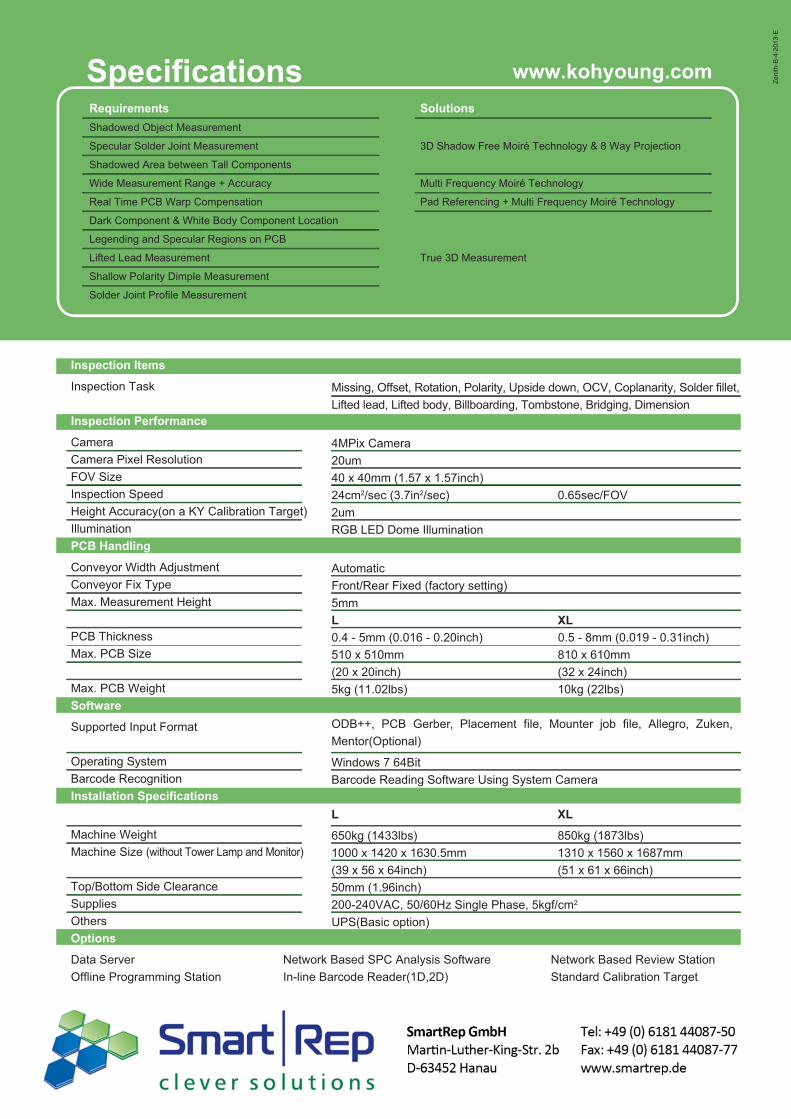
RequirementsShadowed Object Measurement
Specular Solder Joint Measurement
Shadowed Area between Tall Components
Wide Measurement Range + Accuracy
Real Time PCB Warp Compensation
Dark Component & White Body Component Location
Legending and Specular Regions on PCB
Lifted Lead Measurement
Shallow Polarity Dimple Measurement
Solder Joint Profile Measurement
Solutions
3D Shadow Free Moiré Technology & 8 Way Projection
Multi Frequency Moiré Technology
Pad Referencing + Multi Frequency Moiré Technology
True 3D Measurement
Inspection Items
Inspection Task
Inspection Performance
CameraCamera Pixel ResolutionFOV SizeInspection SpeedHeight Accuracy(on a KY Calibration Target)IlluminationPCB Handling
Conveyor Width Adjustment Conveyor Fix Type Max. Measurement Height
Max. PCB Size Max. PCB WeightSoftware
Supported Input Format
Operating SystemBarcode RecognitionInstallation Specifications
Machine WeightMachine Size (without Tower Lamp and Monitor)
Top/Bottom Side ClearanceSuppliesOthersOptions
Data Server Network Based SPC Analysis Software Network Based Review StationOffline Programming Station In-line Barcode Reader(1D,2D) Standard Calibration Target
Above specifications are subject to change without notice
Specifications
Missing, Offset, Rotation, Polarity, Upside down, OCV, Coplanarity, Solder fillet,Lifted lead, Lifted body, Billboarding, Tombstone, Bridging, Dimension
4MPix Camera20um40 x 40mm (1.57 x 1.57inch)24cm2/sec (3.7in2/sec) 0.65sec/FOV 2umRGB LED Dome Illumination
AutomaticFront/Rear Fixed (factory setting)5mmL XL
510 x 510mm 810 x 610mm(20 x 20inch) (32 x 24inch)5kg (11.02lbs) 10kg (22lbs)
ODB++, PCB Gerber, Placement file, Mounter job file, Allegro, Zuken, Mentor(Optional)
Windows 7 64BitBarcode Reading Software Using System Camera
L XL
650kg (1433lbs) 850kg (1873lbs)1000 x 1420 x 1630.5mm 1310 x 1560 x 1687mm(39 x 56 x 64inch) (51 x 61 x 66inch)50mm (1.96inch)200-240VAC, 50/60Hz Single Phase, 5kgf/cm2
UPS(Basic option)
PCB Thickness 0.4 - 5mm (0.016 - 0.20inch) 0.5 - 8mm (0.019 - 0.31inch)