Embed Size (px)
Citation preview
Zaven Kalfayan
Lindsay Hunting
Phyllis Xu
Joy Perkinson

Presentation Outline
Motivation of project
Project goals
Processing and materials
Results
Cost analysis
TechWatch and future work
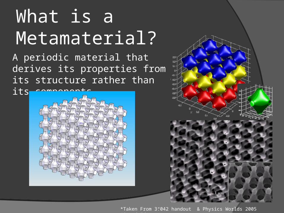
What is a Metamaterial?
A periodic material that derives its properties from its structure rather than its components.
*Taken From 3.042 handout & Physics Worlds 2005 “Sound Ideas”
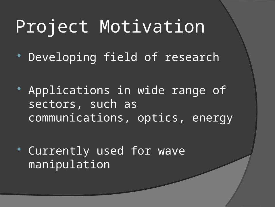
Project Motivation
Developing field of research
Applications in wide range of sectors, such as communications, optics, energy
Currently used for wave manipulation

Project Goals
Design a process using lithography to fabricate a 3D structure
Create macroscale models of 2D structure, phase mask, and 3D structure
Create a 3D metamaterial and image using SEM

Process Design
2-D photoresist
pattern
Phase mask
Sol-gel infiltration
3-D pattern
Titania structure
Interference lithography
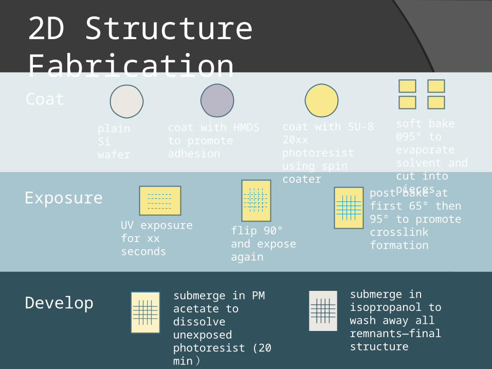
2D Structure Fabrication
Coat
Exposure
Develop
plain Si wafer
coat with HMDS to promote adhesion
coat with SU-8 20xx photoresist using spin coater
soft bake @95° to evaporate solvent and cut into pieces
UV exposure for xx seconds
flip 90° and expose again
post bake at first 65° then 95° to promote crosslink formation
submerge in PM acetate to dissolve unexposed photoresist (20 min)
submerge in isopropanol to wash away all remnants—final structure
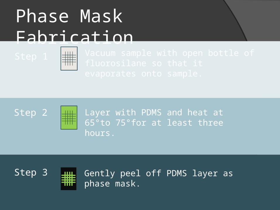
Phase Mask Fabrication
Step 1
Step 2
Step 3
Vacuum sample with open bottle of fluorosilane so that it evaporates onto sample.
Layer with PDMS and heat at 65°to 75°for at least three hours.
Gently peel off PDMS layer as phase mask.
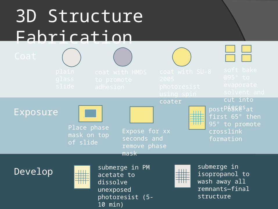
3D Structure Fabrication
Coat
Exposure
Develop
plain glass slide
coat with HMDS to promote adhesion
coat with SU-8 2005 photoresist using spin coater
soft bake @95° to evaporate solvent and cut into pieces
Place phase mask on top of slide
Expose for xx seconds and remove phase mask
post bake at first 65° then 95° to promote crosslink formation
submerge in PM acetate to dissolve unexposed photoresist (5-10 min)
submerge in isopropanol to wash away all remnants—final structure

Process Tuning
Exposure times (contact lithography):SU8-2002: 0.5-25 secondsSU8-2005: 5-40 secondsSU8-2015: 1-45 seconds
Exposure times (interference lithography):3-20 seconds for all samples

Prototype FunctionalityProblems for 2D & 3D patterns
1. Overexposure
2. Unwashed monomer
3. Adhesion problems
4. Inconsistent results
15s SU-8 2015 Top
15s SU-8 2015 Cross

Design Functionality2-D Patterns
5s SU-8 2015 Cross 5s SU-8 2015 Top
• 5s exposure of SU-8 2015
• Coated with HMDS
•Broadband laser filtered at 365nm
•Top down
•Hole spacing - 3.38 um
•Hole length ~1.5um
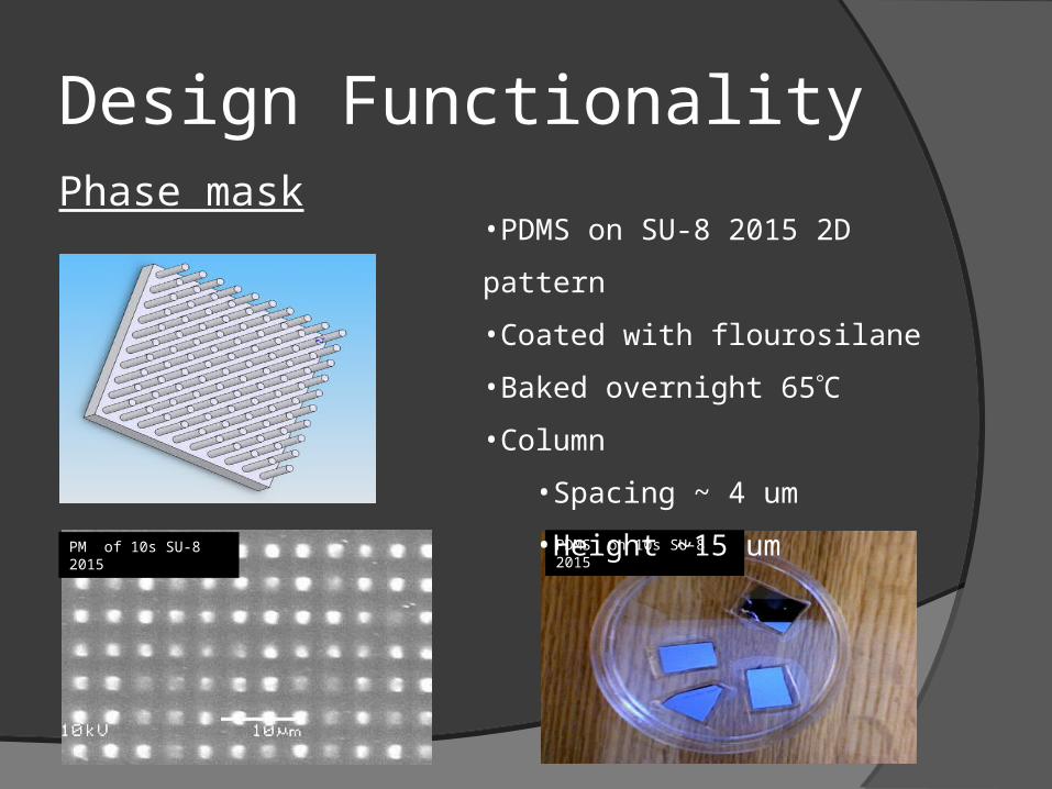
Design FunctionalityPhase mask
PM of 10s SU-8 2015 PDMS on 10s SU-8 2015
•PDMS on SU-8 2015 2D pattern
•Coated with flourosilane
•Baked overnight 65C
•Column
•Spacing ~ 4 um
•Height ~15 um
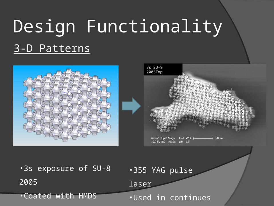
Design Functionality3-D Patterns
3s SU-8 2005Top
•3s exposure of SU-8 2005
•Coated with HMDS
•Thickness ~ 5um
•355 YAG pulse laser
•Used in continues mode
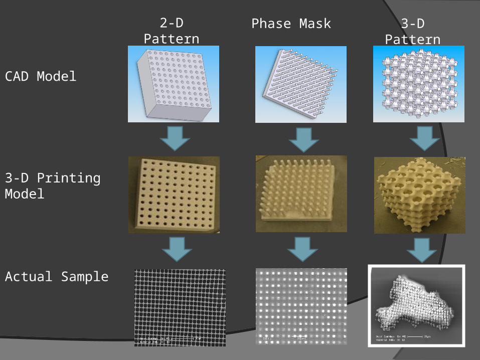
2-D Pattern Phase Mask 3-D Pattern
CAD Model
3-D Printing Model
Actual Sample
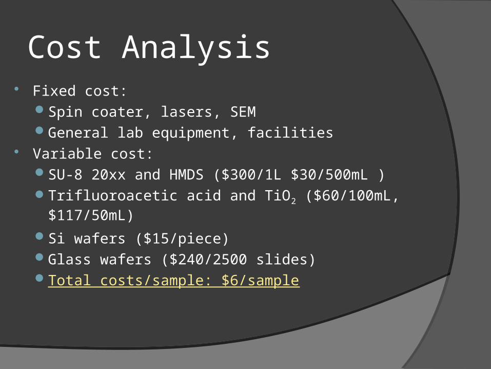
Cost Analysis Fixed cost:
Spin coater, lasers, SEMGeneral lab equipment, facilities
Variable cost:SU-8 20xx and HMDS ($300/1L $30/500mL )Trifluoroacetic acid and TiO2 ($60/100mL, $117/50mL)
Si wafers ($15/piece)Glass wafers ($240/2500 slides)Total costs/sample: $6/sample
Future Work
Optimize process
Explore new thicknesses and exposure
times
Adhesion promoters
Create more complicated 3D structures
Characterize 3D structure properties

TechWatch2004:• Miniaturized antennas based on negative permittivity materials—Lucent Technologies• Metamaterial scanning lens antenna systems and methods—The Boeing Company
2003:• Metamaterials employing photonic crystal—MIT • Methods of fabricating electromagnetic metamaterials—The Boeing Company
2002: • Resonant antennas—Lucent Technologies

Questions?
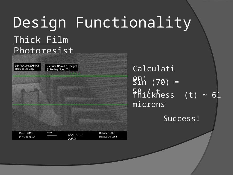
Design Functionality Thick Film Photoresist
Sin (70) = 58 / t
Calculation:
Thickness (t) ~ 61 microns
Success!
45s SU-8 2050
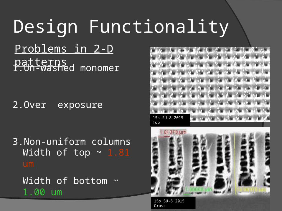
Design FunctionalityProblems in 2-D patterns
1. Un-washed monomer
2. Over exposure
3. Non-uniform columns
Width of top ~ 1.81 um
Width of bottom ~ 1.00 um
15s SU-8 2015 Top
15s SU-8 2015 Cross
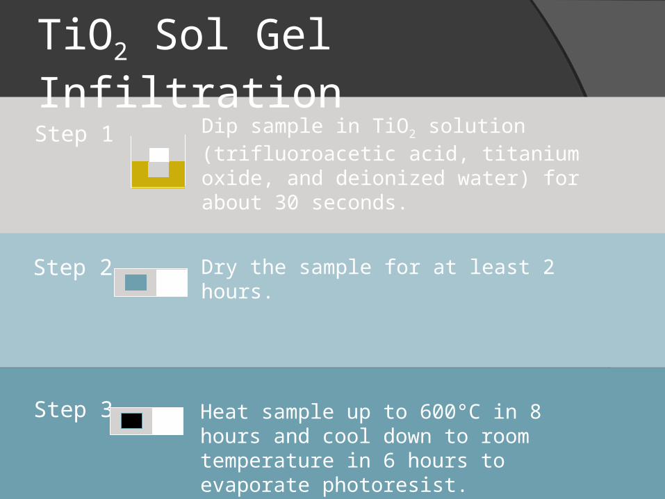
TiO2 Sol Gel Infiltration
Step 1
Step 2
Step 3
Dip sample in TiO2 solution (trifluoroacetic acid, titanium oxide, and deionized water) for about 30 seconds.
Dry the sample for at least 2 hours.
Heat sample up to 600°C in 8 hours and cool down to room temperature in 6 hours to evaporate photoresist.